WO2011083641A1 - 照明装置、表示装置、及びテレビ受信装置 - Google Patents
照明装置、表示装置、及びテレビ受信装置 Download PDFInfo
- Publication number
- WO2011083641A1 WO2011083641A1 PCT/JP2010/071543 JP2010071543W WO2011083641A1 WO 2011083641 A1 WO2011083641 A1 WO 2011083641A1 JP 2010071543 W JP2010071543 W JP 2010071543W WO 2011083641 A1 WO2011083641 A1 WO 2011083641A1
- Authority
- WO
- WIPO (PCT)
- Prior art keywords
- light source
- connector
- led
- side direction
- light
- Prior art date
- Legal status (The legal status is an assumption and is not a legal conclusion. Google has not performed a legal analysis and makes no representation as to the accuracy of the status listed.)
- Ceased
Links
Images






Classifications
-
- G—PHYSICS
- G02—OPTICS
- G02B—OPTICAL ELEMENTS, SYSTEMS OR APPARATUS
- G02B6/00—Light guides; Structural details of arrangements comprising light guides and other optical elements, e.g. couplings
- G02B6/0001—Light guides; Structural details of arrangements comprising light guides and other optical elements, e.g. couplings specially adapted for lighting devices or systems
- G02B6/0011—Light guides; Structural details of arrangements comprising light guides and other optical elements, e.g. couplings specially adapted for lighting devices or systems the light guides being planar or of plate-like form
- G02B6/0081—Mechanical or electrical aspects of the light guide and light source in the lighting device peculiar to the adaptation to planar light guides, e.g. concerning packaging
- G02B6/0083—Details of electrical connections of light sources to drivers, circuit boards, or the like
-
- H—ELECTRICITY
- H04—ELECTRIC COMMUNICATION TECHNIQUE
- H04N—PICTORIAL COMMUNICATION, e.g. TELEVISION
- H04N5/00—Details of television systems
- H04N5/64—Constructional details of receivers, e.g. cabinets or dust covers
-
- H—ELECTRICITY
- H04—ELECTRIC COMMUNICATION TECHNIQUE
- H04N—PICTORIAL COMMUNICATION, e.g. TELEVISION
- H04N5/00—Details of television systems
- H04N5/66—Transforming electric information into light information
-
- G—PHYSICS
- G02—OPTICS
- G02B—OPTICAL ELEMENTS, SYSTEMS OR APPARATUS
- G02B6/00—Light guides; Structural details of arrangements comprising light guides and other optical elements, e.g. couplings
- G02B6/0001—Light guides; Structural details of arrangements comprising light guides and other optical elements, e.g. couplings specially adapted for lighting devices or systems
- G02B6/0011—Light guides; Structural details of arrangements comprising light guides and other optical elements, e.g. couplings specially adapted for lighting devices or systems the light guides being planar or of plate-like form
- G02B6/0081—Mechanical or electrical aspects of the light guide and light source in the lighting device peculiar to the adaptation to planar light guides, e.g. concerning packaging
- G02B6/0086—Positioning aspects
- G02B6/0091—Positioning aspects of the light source relative to the light guide
-
- H—ELECTRICITY
- H01—ELECTRIC ELEMENTS
- H01R—ELECTRICALLY-CONDUCTIVE CONNECTIONS; STRUCTURAL ASSOCIATIONS OF A PLURALITY OF MUTUALLY-INSULATED ELECTRICAL CONNECTING ELEMENTS; COUPLING DEVICES; CURRENT COLLECTORS
- H01R12/00—Structural associations of a plurality of mutually-insulated electrical connecting elements, specially adapted for printed circuits, e.g. printed circuit boards [PCB], flat or ribbon cables, or like generally planar structures, e.g. terminal strips, terminal blocks; Coupling devices specially adapted for printed circuits, flat or ribbon cables, or like generally planar structures; Terminals specially adapted for contact with, or insertion into, printed circuits, flat or ribbon cables, or like generally planar structures
- H01R12/70—Coupling devices
- H01R12/71—Coupling devices for rigid printing circuits or like structures
- H01R12/72—Coupling devices for rigid printing circuits or like structures coupling with the edge of the rigid printed circuits or like structures
- H01R12/721—Coupling devices for rigid printing circuits or like structures coupling with the edge of the rigid printed circuits or like structures cooperating directly with the edge of the rigid printed circuits
Definitions
- the present invention relates to a lighting device, a display device, and a television receiver.
- the display elements of image display devices such as television receivers are shifting from conventional cathode ray tubes to thin display panels such as liquid crystal panels and plasma display panels, which enables thinning of image display devices.
- a backlight device is separately required as a lighting device, and the backlight device is roughly classified into a direct type and an edge light type according to the mechanism.
- an edge light type backlight device it is preferable to use an edge light type backlight device, and an example described in Patent Document 1 below is known.
- the backlight device described in Patent Document 1 includes a light guide plate, an LED facing the end of the light guide plate, an LED substrate on which the LED is mounted, and an LED substrate electrically connected to an external power circuit board. And a lead frame for connecting to the.
- a clip-shaped terminal formed on one end side is soldered to the LED substrate, and a flat-plate terminal formed on the other end side is soldered to an external power supply circuit substrate, so that The power supply is relayed.
- the present invention has been completed based on the above-described circumstances, and an object thereof is to increase the reliability of electrical connection.
- An illumination device includes a light source substrate having a light source and having a longitudinal shape, a chassis in which the light source substrate is accommodated, and a light guide member having an end facing the light source of the light source substrate. And a connector that holds the light source board and is electrically connected to the outside, and is provided with a terminal portion that is electrically connected to the light source. On the other hand, the connector is provided with a connection terminal that comes into contact with the terminal portion in a state in which relative sliding is allowed in the long side direction of the light source substrate.
- connection terminal and the terminal portion can be slid relative to each other in the long side direction of the light source substrate while maintaining the contact state with each other.
- the light source substrate also tends to be elongated in the long side direction, and accordingly, the amount of expansion / contraction increases with thermal expansion or contraction. It can be said that it is suitable for enlargement.
- the terminal portion is formed to be relatively wider than the connection terminal in the long side direction of the light source substrate. In this way, even when the light source board expands or contracts in the long side direction due to thermal expansion or contraction, the terminal part is moved to the long side even when the terminal part and the connection terminal slide relative to each other in the long side direction. Since the direction is relatively wide, the contact state of the connection terminal can be maintained well.
- the terminal portion is wide as described above, since the terminal portion is formed on the light source substrate having a longitudinal shape, it is possible to easily secure the installation space without increasing the size of the light source substrate. Is done. In other words, since the connection terminal on the connector side can be made relatively narrow, it is possible to avoid an increase in size of the connector.
- the connector has a pair of wall portions facing each other while having an insertion groove into which the light source board can be inserted. In this way, when the light source substrate is inserted into the insertion groove of the connector, the light source substrate is sandwiched between the pair of wall portions, thereby holding the light source substrate.
- connection terminal is configured such that a contact portion with respect to the terminal portion protrudes toward the light source substrate from either one of the pair of wall portions. In this way, in a state where the contact portion of the connection terminal protruding from one wall portion side is in contact with the terminal portion, the light source substrate is received by the other wall portion arranged on the side opposite to the connection terminal. Therefore, a good contact state can be obtained.
- the insertion groove is configured to open along the short side direction of the light source substrate. If it does in this way, a light source board can be inserted along a short side direction to a connector.
- a receiving surface for receiving the light source substrate is formed at the back end of the insertion groove.
- the insertion groove is configured to open along the long side direction of the light source substrate. In this way, the light source substrate can be expanded and contracted in the long side direction while being inserted into the insertion groove, so that when the thermal expansion or contraction occurs, the light source substrate is stressed and deformed. Can be avoided.
- the light source substrate has a wiring pattern in which a plurality of the light sources are arranged in parallel in the long side direction and the plurality of light sources are connected in series. If it does in this way, a plurality of light sources can be collectively driven in series by connecting a plurality of light sources in series by a wiring pattern.
- the connector corresponds to the pair of terminal portions. Then, a pair is arranged at two positions separated in the long side direction. In this way, for example, the connector arranged on one end side in the long side direction of the light source board is set as the input side, and the connector arranged on the other end side is set as the output side. A plurality of light sources connected in series can be driven in series. Since the terminal part and the connector are arranged on each end side in the long side direction of the light source board, the distance from the light source located at the end in the long side direction on the light source board to the terminal part can be shortened. Therefore, it can be avoided that the wiring pattern becomes long.
- the terminal portion is disposed at a position that is relatively displaced in the short side direction of the light source substrate with respect to the light source. In this way, it is possible to reduce the size of the light source substrate in the long side direction as compared with the case where the terminal portion and the light source are arranged relatively displaced in the long side direction of the light source substrate.
- the terminal portion is arranged in parallel with the light source in the short side direction. In this way, since the distance between the light source and the terminal portion can be made shorter than when the terminal portion is arranged at a position deviated from the light source in the long side direction, for example, the light source and the terminal When the parts are connected by the wiring pattern, the wiring pattern can be shortened.
- the light source substrate is provided with a wiring pattern in which a plurality of the light sources are arranged in parallel in the long side direction and the plurality of light sources are connected in series, and the terminal portion includes the plurality of light sources. Are arranged in parallel in the short side direction with respect to the light source located at the end in the long side direction. In this way, it is possible to shorten the distance of the wiring pattern routed from the light source located at the end to the terminal portion as compared with the case where the terminal portion is arranged closer to the center than the light source located at the end in the long side direction. it can.
- the light source substrate can be downsized in the longitudinal direction as compared with the case where the terminal portion is arranged further closer to the end than the light source located at the end in the long side direction.
- the light source is eccentrically arranged on one end side in the short side direction in the light source substrate, whereas the terminal portion is on the other end side in the short side direction in the light source substrate. It is arranged eccentrically. If it does in this way, the light source and terminal part which are mutually arranged in the short side direction can be efficiently arranged in the light source substrate.
- the connector can hold the other end of the light source board in the short side direction. If it does in this way, a connector can be kept small about the short side direction of a light source board.
- the chassis has a bottom portion that is disposed on a side opposite to the light emitting side with respect to the light source substrate and the light guide member, and has the bottom portion to which the connector is assembled.
- the connector is arranged at a position off the light guide member in the short side direction of the light source substrate. If it does in this way, it can avoid that a light guide member and a connector mutually interfere.
- the terminal portion is disposed at a position that is relatively displaced in the long side direction of the light source substrate with respect to the light source. In this way, it is possible to reduce the size of the light source substrate in the short side direction as compared with the case where the terminal portion and the light source are arranged relatively displaced in the short side direction of the light source substrate. Thereby, it becomes possible to make the whole said illuminating device thin.
- the terminal portion is formed on the same surface as the surface on which the light source is arranged in the light source substrate. In this way, since the terminal portion and the light source are formed on the same surface of the light source substrate, the light source substrate can be a single-sided mounting type, and the manufacturing cost for the light source substrate can be reduced.
- connection terminal includes an elastic contact piece capable of elastic contact with the terminal portion. If it does in this way, a contact state can be maintained with a favorable contact pressure by making an elastic contact piece elastically contact with a terminal part.
- An assembly hole is formed in the chassis so that the connector can be assembled in a state where the connector penetrates in and out. If it does in this way, the light source board in a chassis can be electrically connected to the exterior via the connector made into the state penetrated in and out of the chassis by being assembled in an assembly hole.
- the connector includes a connector housing that incorporates the connection terminal and has insulation properties. In this way, the connection terminals can be kept insulated from the chassis and the like by the connector housing.
- the connector housing is made of synthetic resin, and the connection terminal is inserted into the connector housing. If it does in this way, the manufacturing cost concerning a connector can be reduced.
- the light source and the end portion of the light guide member arranged to face the light source are arranged apart from each other while holding a space, and are arranged so as to sandwich the space.
- a pair of reflecting members In this way, the light emitted from the light source is repeatedly reflected by the pair of reflecting members in the space held between the opposite ends of the light guide member, so that the light is emitted to the end of the light guide member. On the other hand, it is efficiently incident. Thereby, the utilization efficiency of light can be improved.
- the light source is an LED. In this way, high brightness and low power consumption can be achieved.
- a display device of the present invention includes the above-described illumination device and a display panel that performs display using light from the illumination device.
- a liquid crystal panel can be exemplified as the display panel.
- Such a display device can be applied as a liquid crystal display device to various uses such as a display of a television or a personal computer, and is particularly suitable for a large screen.
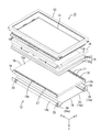
- FIG. 1 is an exploded perspective view showing a schematic configuration of a television receiver according to Embodiment 1 of the present invention.
- the exploded perspective view which shows schematic structure of the liquid crystal display device with which a television receiver is equipped
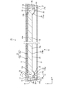
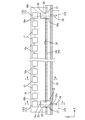
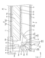
- Sectional drawing which shows the cross-sectional structure along the short side direction of a liquid crystal display device 3 is a cross-sectional view taken along the line iv-iv in FIG. V-v sectional view of FIG.
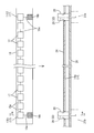
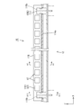
- Vi-vi cross-sectional view of FIG. Partially cutaway sectional view showing the relationship between the connection terminal and the terminal part Sectional view taken along line iv-iv in FIG. 3 showing a state before the LED board is inserted into the connector.
- Sectional drawing which shows cross-sectional structures, such as a LED board based on Embodiment 2 of this invention, a chassis, a connector, and a power supply circuit board.
- Xi-xi sectional view of FIG. Xii-xii sectional view of FIG. The perspective view of the LED board which concerns on other embodiment (1) of this invention.
- FIGS. 1 A first embodiment of the present invention will be described with reference to FIGS.
- the liquid crystal display device 10 is illustrated.
- a part of each drawing shows an X axis, a Y axis, and a Z axis, and each axis direction is drawn to be a direction shown in each drawing.
- the upper side shown in FIG.3 and FIG.4 be a front side, and let the lower side of the figure be a back side.
- the television receiver TV includes a liquid crystal display device 10, front and back cabinets Ca and Cb that are accommodated so as to sandwich the liquid crystal display device 10, a power source P, a tuner T, And a stand S.
- the liquid crystal display device (display device) 10 has a horizontally long (longitudinal) rectangular shape (rectangular shape) as a whole and is accommodated in a vertically placed state.
- the liquid crystal display device 10 includes a liquid crystal panel 11 that is a display panel and a backlight device (illumination device) 12 that is an external light source, which are integrated by a frame-like bezel 13 or the like. Is supposed to be retained.
- the liquid crystal panel 11 has a horizontally long (longitudinal) rectangular shape (rectangular shape) in a plan view, and a pair of glass substrates are bonded together with a predetermined gap therebetween, The liquid crystal is sealed between both glass substrates.
- One glass substrate is provided with a switching element (for example, TFT) connected to a source wiring and a gate wiring orthogonal to each other, a pixel electrode connected to the switching element, an alignment film, and the like.
- the substrate is provided with a color filter and counter electrodes in which colored portions such as R (red), G (green), and B (blue) are arranged in a predetermined arrangement, and an alignment film.
- a polarizing plate is disposed on the outside of both substrates.
- the backlight device 12 covers a substantially box-shaped chassis 14 having an opening that opens toward the light emission surface side (the liquid crystal panel 11 side), and covers the opening of the chassis 14.
- the optical member 15 group (diffusing plate (light diffusing member) 15a and a plurality of optical sheets 15b arranged between the diffusing plate 15a and the liquid crystal panel 11) is provided.
- an LED 17 Light Emitting Diode
- an LED substrate 18 on which the LED 17 is mounted and light from the LED 17 are guided to the optical member 15 (liquid crystal panel 11).
- a frame 16 for holding the light guide member 19 from the front side.
- this backlight apparatus 12 is equipped with the LED board 18 which has LED17 in the both ends of the long side, respectively, and arrange
- the chassis 14 is made of metal, and as shown in FIGS. 2 and 3, a pair of a bottom plate 14a having a horizontally long rectangular shape as in the liquid crystal panel 11 and a pair of rising edges from both outer ends on the long side of the bottom plate 14a. It consists of a side plate 14b.
- the long side direction of the chassis 14 (bottom plate 14a) coincides with the X-axis direction (horizontal direction), and the short side direction coincides with the Y-axis direction (vertical direction).
- the pressing member 16 and the bezel 13 can be screwed to the side plate 14b.
- the detailed shape of the bottom plate 14a will be described in detail later.
- the optical member 15 has a horizontally long rectangular shape when viewed in a plane, like the liquid crystal panel 11 and the chassis 14.
- the optical member 15 is placed on the front side (light emitting side) of the light guide member 19 and is disposed between the liquid crystal panel 11 and the light guide member 19.
- the optical member 15 includes a diffusion plate 15a disposed on the back side (light guide member 19 side, opposite to the light emitting side) and an optical sheet 15b disposed on the front side (liquid crystal panel 11 side, light emitting side). Composed.
- the diffusing plate 15a has a structure in which a large number of diffusing particles are dispersed in a substantially transparent resin-made base material having a predetermined thickness, and has a function of diffusing transmitted light.
- the optical sheet 15b has a sheet shape that is thinner than the diffusion plate 15a, and three optical sheets are laminated.
- Specific types of the optical sheet 15b include, for example, a diffusion sheet, a lens sheet, a reflective polarizing sheet, and the like, which can be appropriately selected and used.
- the frame 16 is formed in a frame shape (frame shape) extending along the outer peripheral end portion of the light guide member 19, and the outer peripheral end portion of the light guide member 19 extends over substantially the entire circumference. It can be pressed from the front side.
- the frame 16 is made of a synthetic resin and has a light shielding property by having a surface with, for example, a black color.
- first reflective sheets 22 that reflect light are respectively provided on the back side surfaces of both long side portions of the frame 16, that is, the surfaces facing the light guide member 19 and the LED substrate 18 (LED 17). It is attached.
- the first reflection sheet 22 has a size extending over substantially the entire length of the long side portion of the frame 16, and is in direct contact with the end portion of the light guide member 19 on the LED 17 side and the light guide member 19.
- the end portion and the LED substrate 18 are collectively covered from the front side.
- the frame 16 can receive the outer peripheral end of the liquid crystal panel 11 from the back side.
- the LED 17 has a configuration in which an LED chip is sealed with a resin material on a substrate portion fixed to the LED substrate 18, as shown in FIGS.
- the LED chip mounted on the substrate unit has one main emission wavelength, and specifically, one that emits blue light in a single color is used.
- the resin material that seals the LED chip is dispersed and blended with a phosphor that emits a predetermined color when excited by the blue light emitted from the LED chip, and generally emits white light as a whole. It is said.
- the phosphor for example, a yellow phosphor that emits yellow light, a green phosphor that emits green light, and a red phosphor that emits red light are used in appropriate combination, or any one of them is used. It can be used alone.
- the LED 17 is a so-called top type in which a surface opposite to the mounting surface with respect to the LED substrate 18 is a light emitting surface.
- the LED substrate 18 is made of a synthetic resin (such as an epoxy resin) or a ceramic, and as shown in FIGS. 2 to 4, along the long side direction of the chassis 14 (the end portion on the LED 17 side of the light guide member 19). It has a long and elongated plate shape, and its main plate surface is parallel to the X-axis direction and Z-axis direction, that is, orthogonal to the plate surfaces of the liquid crystal panel 11 and the light guide member 19 (optical member 15). It is accommodated in the chassis 14 in a different posture.
- the LED board 18 has a posture in which the long side direction on the main plate surface coincides with the X-axis direction, the short side direction coincides with the Z-axis direction, and the plate thickness direction orthogonal to the main plate surface coincides with the Y-axis direction. It is said.
- a pair of LED substrates 18 are arranged at positions sandwiching the light guide member 19 in the Y-axis direction. Specifically, between the light guide member 19 and each side plate 14 b in the chassis 14. The chassis 14 is accommodated from the front side along the Z-axis direction.
- the LED 17 having the above-described configuration is surface-mounted on the inner side, that is, the surface facing the light guide member 19 side (the surface facing the light guide member 19). Since the pair of LED boards 18 are accommodated in the chassis 14 with the mounting surfaces of the LEDs 17 facing each other, the light emitting surfaces of the LEDs 17 respectively mounted on the LED boards 18 are opposed to each other.
- the optical axis of the LED 17 substantially coincides with the Y-axis direction. In other words, the LEDs 17 mounted on the pair of LED substrates 18 are respectively arranged opposite to both ends of the light guide member 19.
- a raw material used for the LED board 18 it is also possible to set it as the structure which used metal materials, such as the same aluminum type material as the chassis 14, for example, and formed the wiring pattern on the surface through the insulating layer.
- a plurality (30 in FIG. 2) of LEDs 17 are arranged in a line (linearly) along the long side direction (X-axis direction) on the mounting surface of the LED substrate 18.
- These LED 17 groups are close to one end in the short side direction of the LED substrate 18 (close to the end opposite to the terminal portion 18b described later), specifically, the frame 16 side (the liquid crystal panel 11 side, the front side). It is arranged eccentrically near the end of the.
- a wiring pattern 18 a made of a metal film (such as a copper foil) is formed on the LED substrate 18 so as to cross the mounted LED 17 group and connect adjacent LEDs 17 in series.
- the wiring pattern 18a linearly crosses between the LED 17E1 positioned at one end in the long side direction of the LED substrate 18 and the LED 17E2 positioned at the other end along the long side direction. Thus, all the mounted LEDs 17 are electrically connected.
- a pair of terminal portions (lands) 18 b connected to the connector 20 are formed near both ends in the long side direction of the LED substrate 18.
- the terminal portion 18b will be described in detail.
- the suffix “E1” is attached to the symbol of the LED located at the left end shown in FIG. 4
- the suffix “E2” is attached to the symbol of the LED located at the right end of FIG. If it is assumed that it is generically referred to without distinction, no subscript is attached. 4 and 7, the wiring pattern 18a is illustrated by a one-dot chain line, and in FIG. 7, the terminal portion 18b is illustrated in a shaded manner.
- the terminal portion 18b is made of a metal film like the wiring pattern 18a, is formed in a square shape (rectangular shape) when viewed from the front, and is a surface of the main plate surface of the LED substrate 18. It has a predetermined area (area slightly smaller than the LED 17).
- the terminal portion 18 b is disposed at a position (separated position) that is relatively displaced with respect to the LED 17 in the Z-axis direction, that is, in the short side direction of the LED substrate 18.
- the terminal portion 18b is arranged at a position parallel to the Z-axis direction with a predetermined distance from each LED 17E1, 17E2 located at both ends in the long side direction on the LED substrate 18.
- Each terminal portion 18b is electrically connected to each LED 17E1, 17E2 located at both ends of the LED substrate 18 in the long side direction by a wiring pattern 18a.
- the portion of the wiring pattern 18a that connects the terminal portion 18b and the LEDs 17E1 and 17E2 has a straight line shape along the Z-axis direction, and the length thereof is equal to the distance between the terminal portion 18b and the LEDs 17E1 and 17E2. .
- the terminal portion 18b is arranged eccentrically toward the other end (closer to the side opposite to the LED 17 side) in the short side direction (Z-axis direction) of the LED substrate 18.
- the chassis 14 is disposed at the end of the bottom plate 14a side (connector 20 side, back side).
- the LED board 18 according to the present embodiment is a single-sided mounting type in which only one side of the main plate surface is a mounting surface.
- the light guide member 19 is made of a synthetic resin material (for example, acrylic or the like) having a refractive index sufficiently higher than air and substantially transparent (excellent in translucency). As shown in FIG. 2, the light guide member 19 is formed in a plate shape having a horizontally long rectangular shape when seen in a plan view like the liquid crystal panel 11 and the chassis 14, and the long side direction on the main plate surface is the X-axis direction. In addition, the short side direction coincides with the Y-axis direction, and the plate thickness direction perpendicular to the main plate surface coincides with the Z-axis direction. As shown in FIG.
- the light guide member 19 is disposed in the chassis 14 at a position immediately below the liquid crystal panel 11 and the optical member 15, and a pair of LED substrates disposed at both ends of the long side of the chassis 14. 18 are arranged so as to be sandwiched between them in the Y-axis direction. Therefore, the alignment direction of the LED 17 (LED substrate 18) and the light guide member 19 coincides with the Y-axis direction, whereas the alignment direction of the optical member 15 (liquid crystal panel 11) and the light guide member 19 is the Z-axis direction. And the arrangement directions of the two are orthogonal to each other.
- the light guide member 19 introduces light emitted from the LED 17 in the Y-axis direction, and rises and emits the light toward the optical member 15 side (Z-axis direction) while propagating the light inside. It has a function. Since the light guide member 19 is arranged at the center position in the short side direction of the bottom plate 14a of the chassis 14, the light guide member in which the center portion in the short side direction of the bottom plate 14a supports the light guide member 19 from the back side. A support portion 23 is provided.
- the light guide member 19 is formed to be slightly larger than the optical member 15 described above, and its outer peripheral end projects outward from the outer peripheral end surface of the optical member 15 and is pressed by the frame 16 described above. (FIG. 3).
- the surface facing the front side of the main plate surface of the light guide member 19 is a light emitting surface 19a for emitting internal light toward the optical member 15 and the liquid crystal panel 11, as shown in FIG.
- a light emitting surface 19a for emitting internal light toward the optical member 15 and the liquid crystal panel 11, as shown in FIG.
- both end surfaces on the long side that are long along the X-axis direction are opposed to the LED 17 (LED substrate 18) with a predetermined space therebetween.
- the first reflection sheet 22 described above is arranged, whereas on the back side of the space, The second reflection sheet 24 is disposed so as to sandwich the same space with the first reflection sheet 22.
- Both reflection sheets 22 and 24 are arranged in such a manner as to sandwich the LED 17 side end portion of the light guide member 19 and the LED 17 in addition to the above space.
- the light from LED17 can be efficiently incident with respect to the light-incidence surface 19b by repeatedly reflecting between both the reflective sheets 22 and 24.
- the light incident surface 19b is a surface parallel to the X-axis direction and the Z-axis direction (the main plate surface of the LED substrate 18), and is a surface substantially orthogonal to the light emitting surface 19a. Further, the alignment direction of the LED 17 and the light incident surface 19b coincides with the Y-axis direction and is parallel to the light emitting surface 19a.
- a light guide reflection sheet 25 that can reflect the light in the light guide member 19 and rise up to the front side covers the entire area.
- a reflecting portion (not shown) that reflects internal light or a scattering portion that scatters internal light (see FIG. (Not shown) is patterned so as to have a predetermined in-plane distribution, and thereby, the emitted light from the light emitting surface 19a is controlled to have a uniform distribution in the surface.
- the connector 20 corresponds to a pair of terminal portions 18 b arranged in the vicinity of both ends in the long side direction of each LED board 18 and in the vicinity of both ends in the long side direction of the chassis 14. Are arranged in pairs.
- the connector 20 is held in a state of penetrating the bottom plate 14 a in and out by being assembled in an assembly hole 14 c formed in the bottom plate 14 a of the chassis 14.
- a portion protruding into the chassis 14 is an LED substrate side connecting portion 20 a that can be connected to the LED substrate 18, whereas a portion protruding outside the chassis 14 is connected to the external power circuit board 21.
- the power supply circuit board side connecting portion 20b is connectable to the power circuit board side.
- the protruding tip portion into the chassis 14 in the LED board side connection portion 20a is displaced from the light guide member 19 in a position lower than the light guide member 19, that is, in the Z-axis direction (the short side direction of the LED board 18). It is arranged at a position, thereby avoiding a situation in which interference with the light guide member 19 occurs.
- the connectors 20 are arranged in pairs near the positions of both ends in the short side direction on the bottom plate 14a of the chassis 14, both ends in the short side direction of the bottom plate 14a excluding the light guide member support portion 23 are provided.
- a connector assembling portion 26 to which the connector 20 is assembled is provided.
- the connector assembling portion 26 rises from the light guide member support portion 23 toward the back side and is inclined, and an outer end portion protruding outward from the rising end of the rising portion 26a along the Y-axis direction. 26b.
- the outer end portion 26b is parallel to the light guide member support portion 23 and has an assembly hole 14c, and the side plate 14b rises from the outer end.
- a pair of assembly holes 14c are formed near both ends in the X-axis direction of the outer end portion 26b (FIG. 4).
- the second reflection sheet 24 described above is disposed along the inner surface of the connector assembly portion 26 and is disposed in a range straddling the rising portion 26a and the outer end portion 26b (FIG. 5).
- the connector 20 includes a connector housing 27 and connection terminals 28 inserted (embedded) in the connector housing 27.
- the connector housing 27 is made of a synthetic resin having insulating properties, and has a substantially block shape as a whole.
- a portion of the connector housing 27 that protrudes into the chassis 14, that is, a portion that constitutes the LED board side connection portion 20 a, has a pair of walls that are opposed to each other while having an insertion groove 29 into which the LED board 18 can be inserted. Portions 30 and 31 are formed.
- the insertion groove 29 is configured to open toward the front side along the Z-axis direction (the short side direction of the LED substrate 18) and open to both sides along the X-axis direction (the long side direction of the LED substrate 18).
- the LED substrate 18 can be inserted into the insertion groove 29 along the short side direction (Z-axis direction) from the front side, and both ends of the LED substrate 18 in the long side direction (X-axis direction) in the inserted state.
- the portion is exposed to the outside of the connector 20 and can be displaced relative to the connector 20 along the long side direction (X-axis direction).
- a receiving surface 29a for receiving the LED board 18 to be inserted is formed at the back end of the insertion groove 29, whereby the insertion depth of the LED board 18 can be regulated, and thus the LED in the Z-axis direction can be regulated.
- the positional relationship between the substrate 18 and the connector 20 can be kept constant.
- the pair of wall portions 30 and 31 are arranged in such a manner that the LED substrate 18 inserted into the insertion groove 29 is sandwiched from the front and back in the Y-axis direction.
- the outer wall portion 30 is disposed on the side plate 14b side, and the inner wall portion 31 is disposed on the inner side in the short side direction (the light guide member 19 side).
- the outer wall portion 30 can be supported by contacting the surface of the main plate surface of the LED substrate 18 opposite to the mounting surface of the LED 17 and the terminal portion 18b.
- the inner wall portion 31 is disposed in an opposing manner at a position with a predetermined gap between the LED 17 and the mounting surface of the terminal portion 18b on the main plate surface of the LED substrate 18.
- the LED substrate 18 inserted into the insertion groove 29 is held between the wall portions 30 and 31 at the other end portion in the short side direction, that is, the end portion where the terminal portion 18b is disposed. Further, holding projections 32 that can hold the connector 20 from the chassis 14 in a state of being prevented from coming off by being locked to the edge of the assembly hole 14 c of the chassis 14 on the outer surfaces of both the wall portions 30 and 31, respectively. A pair is formed.
- connection terminal 28 is made of metal having excellent conductivity, and is embedded in a shape penetrating the connector housing 27 along the Z-axis direction.
- one end side arranged in the chassis 14 is an elastic contact piece 33 constituting the LED board side connection portion 20a, whereas the other end side arranged outside the chassis 14 is connected to the power circuit board side.
- the tab portion 34 constitutes the portion 20b. Of these, the tab portion 34 protrudes further from the connector housing 27 toward the back side, and is inserted into an insertion hole 21 a formed in the power supply circuit board 21.
- a power supply side connector 21b is assembled to the power supply circuit board 21, and a tab portion 34 is electrically connected to the power supply side connector 21b. 3 to 7, the power supply side connector 21b is indicated by a two-dot chain line.
- the elastic contact piece 33 is arranged so as to be exposed in the insertion groove 29 by projecting from the inner wall portion 31 side to the outer wall portion 30 side, that is, the LED substrate 18 side to be inserted, in the connector housing 27.
- the shape is substantially V-shaped.
- the elastic contact piece 33 can be elastically deformed with a base end protruding from the connector housing 27 as a fulcrum.
- the protruding tip portion toward the LED substrate 18 serves as a contact 33a for the terminal portion 18b.
- the contact 33a is disposed at a position where the distance between the contact wall 33a and the outer wall 30 is slightly smaller than the thickness of the LED board 18 (FIG. 9).
- the elastic contact piece 33 is elastically deformed while opening as the contact 33a contacts the terminal portion 18b. Accordingly, the LED substrate 18 can be mechanically held between the outer wall portion 30 and the elastic contact piece 33 with a predetermined contact with the terminal portion 18b by the elastic force acting from the elastic contact piece 33. It is possible to keep in contact with pressure.
- the elastic contact piece 33 of the connection terminal 28 is elastically brought into contact with the terminal portion 18b of the LED substrate 18 so that the electrical connection state is maintained. Since the elastic contact piece 33 and the terminal portion 18b are not fixed by soldering or the like, they can be relatively slid along the surface of the terminal portion 18b while maintaining the mutual contact state. . Therefore, for example, even when the LED board 18 expands or contracts in the long side direction (X-axis direction) due to thermal expansion or contraction, the terminal portion 18b remains in contact with the elastic contact piece 33 while maintaining the X-axis. It is possible to slide relative to the direction. Thereby, the expansion / contraction of the LED board 18 accompanying thermal expansion or thermal contraction can be allowed without causing poor contact.
- the terminal portion 18b has a relatively larger dimension in the X-axis direction than the elastic contact piece 33 (connection terminal 28). That is, the terminal portion 18 b is formed wider than the elastic contact piece 33 (connection terminal 28) in the long side direction of the LED substrate 18.
- the elastic contact piece 33 is brought into contact with the terminal portion 18b at a substantially central position in the X-axis direction and elastic.
- a margin portion of the terminal portion 18b is secured by a predetermined width.
- the elastic contact piece 33 The contact state is maintained by contacting the margin portion of the terminal portion 18b.
- the dimension of the X-axis direction in the terminal part 18b is set to the magnitude
- This embodiment has the structure as described above, and its operation will be described next.
- the separately manufactured liquid crystal panel 11, backlight device 12, bezel 13 and the like are assembled.
- a manufacturing procedure of the liquid crystal display device 10 will be described.
- the connector 20 is assembled, the connector 20 is inserted into the assembly hole 14c in the connector assembly portion 26 (end portion in the short side direction) of the bottom plate 14a of the chassis 14 from the back side. Then, as shown in FIGS. 8 and 9, the holding protrusion 32 is locked from the front side with respect to the edge of the assembly hole 14c, so that the connector 20 is pulled out in a state of penetrating inward and outward with respect to the chassis 14. Stopped and held.
- the second reflection sheet 24 is laid along the connector assembly portion 26 in the bottom plate 14a, and is disposed between the pair of connectors 20 arranged in the X-axis direction (FIG. 8).
- the light guide member 19 is placed on the light guide member support portion 23 (the central portion in the short side direction) of the bottom plate 14a with the light guide reflection sheet 25 attached to the back surface 19c.
- the LED substrate 18 is assembled.
- the LED substrate 18 is assembled along the Z-axis direction (the short side direction of the LED substrate 18) from the front side between the side plate 14b of the chassis 14 and the light incident surface 19b of the light guide member 19. This operation is performed while aligning the respective terminal portions 18b disposed on both ends of the LED substrate 18 in the long side direction with respect to the respective connectors 20 in the X-axis direction.
- the contact portion 33a of the elastic contact piece 33 exposed in the insertion groove 29 becomes the terminal portion 18b.
- the elastic contact piece 33 is elastically opened and deformed.
- the light guide member 19 is held from the front side, and the optical members 15 are placed on the light guide member 19, and then the liquid crystal panel 11 and the bezel 13 are sequentially assembled.
- the power circuit board 21 is fixed to the back side of the chassis 14 with screws or the like.
- the tab portion 34 of the connection terminal 28 in the connector 20 is inserted into the insertion hole 21 a in the power circuit board 21.
- the connector 20 is electrically connected to the power supply side connector 21 b of the power supply circuit board 21. That is, the power supply circuit board 21 is electrically connected to each LED 17 on the LED board 18 via the connector 20.
- the space is optically closed by the first reflective sheet 22 on the front side and the second reflective sheet 24 on the back side. Therefore, the light from the LED 17 is repeatedly reflected by both the reflection sheets 22 and 24, and efficiently enters the light incident surface 19b without leaking to the outside.
- each LED 17 is turned on, so that the temperature environment in the backlight device 12 changes.
- This change in temperature environment tends to become larger as the screen size of the liquid crystal display device 10 becomes larger and the number of LEDs 17 used in association therewith increases.
- the LED substrate 18 in order to increase the number of LEDs 17 to be installed, the LED substrate 18 must have a larger long side dimension. Therefore, the LED substrate 18 has a long side direction when thermal expansion or contraction occurs. The amount of expansion / contraction becomes larger.
- a contact failure may occur due to cracks in the soldered portion due to the expansion and contraction of the LED substrate 18.
- connection terminal 28 of the connector 20 is brought into contact with the terminal portion 18b of the LED board 18 in a state where relative sliding is allowed in the long side direction of the LED board 18.
- the terminal portion 18 b is wider in the X-axis direction than the elastic contact piece 33 of the connection terminal 28, and has a margin portion on both sides of the elastic contact piece 33. ing. Therefore, thermal expansion or thermal contraction occurs in the LED substrate 18 from this state, and the LED substrate 18 expands and contracts in the long side direction (X-axis direction). Accordingly, the terminal portion 18b is relatively relative to the elastic contact piece 33 in the X-axis direction. Even when it slides, both 18b and 33 are reliably maintained in a contact state. As a result, a contact failure between the LED board 18 and the connector 20 can be avoided, and high connection reliability can be obtained.
- the backlight device 12 includes the LED 17 that is the light source and the LED board 18 that has a long shape, the chassis 14 that houses the LED board 18, and the LEDs 17 of the LED board 18.
- the light guide member 19 having end portions arranged opposite to each other and a connector 20 that is assembled to the chassis 14 and that holds the LED substrate 18 and is electrically connected to the outside are provided.
- the connector 20 is provided with a terminal 18b that is electrically connected to the connector 20, while the connector 20 is connected to the terminal 18b in a state in which relative sliding is allowed in the long side direction of the LED board 18. Is provided.
- connection terminal 28 and the terminal portion 18b are relatively slidable in the long side direction of the LED board 18 while maintaining the contact state with each other, so that the contact failure is caused. It can be avoided.
- the LED board 18 when the backlight device 12 is enlarged, the LED board 18 also tends to be elongated in the long side direction, and accordingly, the amount of expansion / contraction increases with thermal expansion or contraction, It can be said that this embodiment is suitable for enlargement. Thus, according to this embodiment, the reliability of electrical connection can be increased.
- the terminal portion 18 b is formed to be relatively wider than the connection terminal 28 in the long side direction of the LED substrate 18. In this way, even when the LED substrate 18 expands or contracts in the long side direction due to thermal expansion or contraction, the terminal portion 18b and the connection terminal 28 slide relative to each other in the long side direction. Since 18b is relatively wide in the long side direction, the contact state of the connection terminal 28 can be maintained satisfactorily.
- the terminal portion 18b is wide as described above, since the terminal portion 18b is formed on the LED substrate 18 having a longitudinal shape, the installation space can be easily secured without increasing the size of the LED substrate 18. Is possible. In other words, since the connection terminal 28 on the connector 20 side can be made relatively narrow, it is possible to avoid an increase in the size of the connector 20.
- the connector 20 has a pair of wall portions 30 and 31 that are opposed to each other while having an insertion groove 29 into which the LED board 18 can be inserted. In this way, when the LED board 18 is inserted into the insertion groove 29 of the connector 20, the LED board 18 is sandwiched between the pair of wall portions 30 and 31, thereby holding the LED board 18.
- connection terminal 28 a contact portion (elastic contact piece 33) with respect to the terminal portion 18 b protrudes toward the LED substrate 18 from the inner wall portion 31 side which is one of the pair of wall portions 30 and 31. Formed.
- the LED board 18 is arranged on the opposite side to the connection terminal 28. Since it is received by the outer wall portion 30 which is the other wall portion, a good contact state can be obtained.
- the insertion groove 29 is configured to open along the short side direction of the LED substrate 18. In this way, the LED board 18 can be inserted into the connector 20 along the short side direction.
- a receiving surface 29 a that receives the LED substrate 18 is formed at the back end of the insertion groove 29.
- the LED board 18 can be positioned with respect to the connector 20 in the insertion direction. At this time, it is possible to position the LED 17 of the LED substrate 18 with respect to the end of the light guide member 19, thereby allowing light from the LED 17 to enter the light guide member 19 satisfactorily. .
- the insertion groove 29 is configured to open along the long side direction of the LED substrate 18. In this way, the LED substrate 18 can be expanded and contracted in the long side direction in the state of being inserted into the insertion groove 29. Therefore, when the thermal expansion or contraction occurs, the LED substrate 18 is stressed and deformed. Can be avoided.
- the LED board 18 is formed with a wiring pattern 18a in which a plurality of LEDs 17 are arranged in parallel in the long side direction and the plurality of LEDs 17 are connected in series. If it does in this way, the some LED17 can be collectively driven in series by connecting the some LED17 in series by the wiring pattern 18a.
- the terminal portion 18b is formed on one end side and the other end side in the long side direction on the LED board 18, respectively, whereas the connector 20 corresponds to the pair of terminal portions 18b.
- a pair is arranged at two positions separated in the long side direction.
- the connector 20 arranged on one end side in the long side direction of the LED board 18 is set as the input side
- the connector 20 arranged on the other end side is set as the output side.
- a plurality of LEDs 17 connected in series by the wiring pattern 18a can be driven in series. Since the terminal portion 18b and the connector 20 are respectively arranged on each end side in the long side direction of the LED substrate 18, the distance from the LED 17 located at the end in the long side direction to the terminal portion 18b on the LED substrate 18 is short. Therefore, it is possible to avoid the wiring pattern 18a from becoming long.
- the terminal portion 18b is disposed at a position relatively displaced in the short side direction of the LED substrate 18 with respect to the LED 17.
- the LED board 18 can be reduced in size in the long side direction as compared with the case where the terminal portion and the LED are arranged relatively displaced in the long side direction of the LED board 18.
- the terminal portion 18b is arranged in parallel with the LED 17 in the short side direction. In this way, the distance between the LED 17 and the terminal portion 18b can be made shorter compared to the case where the terminal portion is arranged at a position deviated from the LED 17 in the long side direction.
- the wiring pattern 18a can be short.
- the LED substrate 18 is provided with a plurality of LEDs 17 arranged in parallel in the long side direction and a wiring pattern 18 a that connects the plurality of LEDs 17 in series.
- the terminal portion 18 b is a long side of the plurality of LEDs 17.
- the LEDs 17E1 and 17E2 located at the end of the direction are arranged in parallel in the short side direction.
- the LED board 18 can be reduced in size in the longitudinal direction, as compared with the case where the terminal portion is arranged closer to the end than the LEDs 17E1 and 17E2 located at the ends in the long side direction.
- the LED 17 is arranged eccentrically on one end side in the short side direction on the LED substrate 18, whereas the terminal portion 18 b is arranged eccentrically on the other end side in the short side direction on the LED substrate 18. ing. If it does in this way, LED17 and terminal part 18b which are arranged mutually shifted in the direction of a short side can be efficiently arranged in LED board 18.
- the connector 20 can hold the other end of the LED substrate 18 in the short side direction. In this way, the connector 20 can be kept small in the short side direction of the LED substrate 18.
- the chassis 14 has a bottom plate 14 a that is disposed on the opposite side to the light emitting side with respect to the LED substrate 18 and the light guide member 19 and to which the connector 20 is assembled.
- the bottom plate 14 a is a light guide member 19.
- the light guide member support portion 23 that supports the connector 20 and the connector assembly portion 26 to which the connector 20 is assembled are provided.
- the connector assembly portion 26 projects outward from the light guide member support portion 23. Since the LED board 18 and the terminal portion 18b are arranged so as to be relatively displaced in the short side direction, the LED substrate 18 tends to be large in the short side direction.
- the connector assembly 26 of the chassis 14 is configured to protrude outward from the light guide member support 23, so that a sufficient installation space for the LED board 18 is provided in the chassis 14. Can be secured.
- the connector 20 is disposed at a position deviated from the light guide member 19 in the short side direction of the LED substrate 18. In this way, it is possible to avoid the light guide member 19 and the connector 20 from interfering with each other.
- the terminal part 18b is formed in the same surface as the surface where LED17 was distribute
- the LED substrate 18 can be a single-sided mounting type, and the manufacturing cost related to the LED substrate 18 can be reduced.
- connection terminal 28 has an elastic contact piece 33 capable of elastic contact with the terminal portion 18b. If it does in this way, a contact state can be maintained with a favorable contact pressure by making elastic contact piece 33 elastically contact with terminal part 18b.
- the chassis 14 is formed with an assembly hole 14c that can be assembled with the connector 20 penetrating in and out.
- the LED board 18 in the chassis 14 is electrically connected to the outside via the connector 20 that is assembled in the assembly hole 14c and penetrates into and out of the chassis 14. Can do.
- the connector 20 has a connector housing 27 having a built-in connection terminal 28 and an insulating property. In this way, the connector housing 27 can keep the connection terminal 28 insulated from the chassis 14 and the like.
- the connector housing 27 is made of synthetic resin, and the connection terminals 28 are inserted into the connector housing 27. If it does in this way, the manufacturing cost concerning connector 20 can be reduced.
- LED17 and the edge part of the light guide member 19 distribute
- the light emitted from the LED 17 is repeatedly reflected by the pair of reflection sheets 22 and 24 in the space held between the end portions of the opposing light guide member 19, so that the light guide member It is efficiently incident on the end of 19. Thereby, the utilization efficiency of light can be improved.
- the light source is the LED 17. In this way, high brightness and low power consumption can be achieved.
- the terminal portion 118 b is arranged at a position relatively displaced in the long side direction (X-axis direction) with respect to the LED 17 on the LED substrate 118. Specifically, the terminal portion 118b is arranged closer to the end of the LED board 18 than the LEDs 17E1 and 17E2 located at the ends in the long side direction, and is arranged in parallel with the LEDs 17E1 and 17E2 in the X-axis direction. Has been. As shown in FIGS. 11 and 12, it can be said that the terminal portion 118 b is disposed so as to overlap the LED 17 in the Z-axis direction. In this way, the short side dimension of the LED substrate 118 can be made smaller than in the first embodiment.
- the backlight device 12 and the liquid crystal display device 10 can be reduced in size in the Z-axis direction, that is, thinner.
- the bottom plate 114a has a flat shape over the entire region from the light guide member support portion 123 to the connector assembly portion 126.
- the terminal portion 118 b is arranged at a position that is relatively displaced in the long side direction of the LED substrate 118 with respect to the LED 17.
- the LED board 118 is smaller in the short side direction than in the case where the terminal portions 18b and the LEDs 17 are relatively displaced in the short side direction of the LED board 18 as in the first embodiment.
- the entire backlight device 12 can be reduced in thickness.
- the LED mounted on the LED substrate may have the following configuration.
- the lens member 35 is interposed between the LED 17 ′ and the light incident surface of the light guide member, and has a light emitting surface that is convex toward the light guide member side.
- the LED substrate is sandwiched between the pair of wall portions of the connector.
- the inner wall portion can be omitted.
- the outer wall portion can be omitted, and in this case, for example, the LED substrate may be received by a side plate of the chassis.
- the terminal portion is formed wider than the elastic contact piece in the long side direction of the LED substrate.
- the elastic contact piece is longer than the terminal portion. What formed wide about the side direction is also contained in this invention.
- the LED substrate is of a single-sided mounting type, but a double-sided mounting type is also possible.
- the LED may be formed on one surface of the LED substrate, and the terminal portion may be formed on the other surface.
- the insertion groove opens in both the Z-axis direction and the X-axis direction.
- the insertion groove is closed in the X-axis direction and opened only in the Z-axis direction. It is also possible to do.
- the present invention also includes an arrangement that is deviated.
- the present invention includes an arrangement in which the terminal portion is arranged in the Z-axis direction with respect to the LED located closer to the center than the LED located at the end in the long side direction of the LED substrate.
- a blue LED chip that emits blue light in a single color and a type of LED that emits substantially white light using a phosphor has been described.
- ultraviolet light blue-violet light
- the present invention also includes an LED chip that incorporates an LED chip that emits monochromatic light and that emits substantially white light using a phosphor.
- the present invention includes an LED using a type of LED in which three types of LED chips each emitting C (cyan), M (magenta), and Y (yellow) are monochromatic.
- a pair of LED substrates are arranged at the ends of both long sides of the chassis (light guide member).
- the LED substrate is a chassis (
- the present invention also includes a pair of light guide members provided at the ends on both short sides.
- LED substrates (10) In addition to the above (9), a pair of LED substrates (LEDs) arranged on both ends of the long side and the short side of the chassis (light guide member), and conversely, the LED substrate A structure in which one (LED) is arranged only for one end of one long side or one short side of the chassis (light guide member) is also included in the present invention.
- the TFT is used as the switching element of the liquid crystal display device.
- the present invention can also be applied to a liquid crystal display device using a switching element other than TFT (for example, a thin film diode (TFD)), and color display.
- a switching element other than TFT for example, a thin film diode (TFD)
- TFT thin film diode
- the present invention can be applied to a liquid crystal display device that displays black and white.
- the liquid crystal display device using the liquid crystal panel as the display panel has been exemplified.
- the present invention can also be applied to a display device using another type of display panel.
- the television receiver provided with the tuner is illustrated, but the present invention can be applied to a display device that does not include the tuner.
- SYMBOLS 10 Liquid crystal display device (display device), 11 ... Liquid crystal panel (display panel), 12 ... Backlight device (illumination device), 14 ... Chassis, 14a ... Bottom plate (bottom part), 14c ... Assembly hole, 17 ... LED ( Light source), 18 ... LED substrate (light source substrate), 18a ... wiring pattern, 18b ... terminal portion, 19 ... light guide member, 20 ... connector, 22 ... first reflective sheet (reflective member), 23 ... light guide member support portion , 24 ... 2nd reflection sheet (reflection member), 26 ... Connector assembly part, 27 ... Connector housing, 28 ... Connection terminal, 29 ... Insertion groove, 30 ... Outer wall part (wall part), 31 ... Inner wall part (wall part) 33 ... elastic contact piece, TV ... TV receiver
Landscapes
- Physics & Mathematics (AREA)
- Engineering & Computer Science (AREA)
- Multimedia (AREA)
- Signal Processing (AREA)
- General Physics & Mathematics (AREA)
- Optics & Photonics (AREA)
- Planar Illumination Modules (AREA)
Abstract
照明装置において電気的接続の信頼性を向上させることを目的とする。本発明に係るバックライト装置(12)は、光源であるLED(17)を有するとともに長手状をなすLED基板(18)と、LED基板(18)が収容さ れるシャーシ(14)と、LED基板(18)のLED(17)に対して端部が対向状に配される導光部材(19)と、シャーシ(14)に組み付けられるとともに、LED基板(18)を保持し且つ外部との電気的接続を図る コネクタ(20)とを備え、LED基板(18)には、LED(17)に電気的に接続された端子部(18b)が設けられるのに対し、コネクタ(20)には、LED基板(18)の長辺方向について相対的なスライドが許容された状態で端子部(18b)に接触される接続端子(28)が設けられている。
Description
本発明は、照明装置、表示装置、及びテレビ受信装置に関する。
近年、テレビ受信装置をはじめとする画像表示装置の表示素子は、従来のブラウン管から液晶パネルやプラズマディスプレイパネルなどの薄型の表示パネルに移行しつつあり、画像表示装置の薄型化を可能としている。液晶表示装置は、これに用いる液晶パネルが自発光しないため、別途に照明装置としてバックライト装置を必要としており、バックライト装置はその機構によって直下型とエッジライト型とに大別されている。液晶表示装置の一層の薄型化を実現するには、エッジライト型のバックライト装置を用いるのが好ましく、その一例として下記特許文献1に記載されたものが知られている。
この特許文献1に記載のバックライト装置は、導光板と、導光板の端部に対して対向状をなすLEDと、LEDを実装したLED基板と、LED基板を外部の電源回路基板に電気的に接続するためのリードフレームとを備える。リードフレームは、一端側に形成されたクリップ形状端子がLED基板に半田付けされるとともに、他端側に形成された平板状端子が外部の電源回路基板に半田付けされることで、LED基板への電力供給を中継するものとされる。
(発明が解決しようとする課題)
ところで、近年では、液晶表示装置の画面サイズの大型化が進行しており、それに伴って液晶表示装置の各構成部材が大型化するとともに、バックライト装置において光源の設置数を増加させる必要があることからバックライト装置全体としての発熱量が増加する傾向にある。このため、大型の液晶表示装置では、使用に伴ってバックライト装置内の温度環境が大きく変化し、それに伴う各構成部材の熱膨張または熱収縮による伸縮量も大きなものとなる。
ところで、近年では、液晶表示装置の画面サイズの大型化が進行しており、それに伴って液晶表示装置の各構成部材が大型化するとともに、バックライト装置において光源の設置数を増加させる必要があることからバックライト装置全体としての発熱量が増加する傾向にある。このため、大型の液晶表示装置では、使用に伴ってバックライト装置内の温度環境が大きく変化し、それに伴う各構成部材の熱膨張または熱収縮による伸縮量も大きなものとなる。
ところが、上記した特許文献1に記載されたものでは、LED基板及び電源回路基板に対するリードフレームの接続方法として半田付けを採用しているため、大型化した場合においてバックライト装置内の温度環境が大きく変化すると、電源回路基板とLED基板とで熱膨張率が相違することに起因して両者間に大きな相対変位が生じ、その結果、半田付け部分に応力が作用してクラックが入ってしまい、電気的接続の信頼性が低下する可能性があった。つまり、上記した特許文献1においては、大型化並びに発熱量の増大化への対応策に関しては、十分な検討がなされていない、というのが現状であった。
本発明は上記のような事情に基づいて完成されたものであって、電気的接続の信頼性を高いものとすることを目的とする。
(課題を解決するための手段)
本発明の照明装置は、光源を有するとともに長手状をなす光源基板と、前記光源基板が収容されるシャーシと、前記光源基板の前記光源に対して端部が対向状に配される導光部材と、前記シャーシに組み付けられるとともに、前記光源基板を保持し且つ外部との電気的接続を図るコネクタとを備え、前記光源基板には、前記光源に電気的に接続された端子部が設けられるのに対し、前記コネクタには、前記光源基板の長辺方向について相対的なスライドが許容された状態で前記端子部に接触される接続端子が設けられている。
本発明の照明装置は、光源を有するとともに長手状をなす光源基板と、前記光源基板が収容されるシャーシと、前記光源基板の前記光源に対して端部が対向状に配される導光部材と、前記シャーシに組み付けられるとともに、前記光源基板を保持し且つ外部との電気的接続を図るコネクタとを備え、前記光源基板には、前記光源に電気的に接続された端子部が設けられるのに対し、前記コネクタには、前記光源基板の長辺方向について相対的なスライドが許容された状態で前記端子部に接触される接続端子が設けられている。
このように、シャーシに対して組み付けられたコネクタに光源基板を保持させると、外部との電気的接続が図られるとともに、光源基板の光源が導光部材の端部に対して対向状に配された状態に保たれる。ここで、光源基板が熱膨張または熱収縮に伴って長辺方向に伸縮した場合、従来ではリードフレームを光源基板に半田付けしているため、半田付け部分に応力が作用してクラックが生じるおそれがあるのに比べると、本発明では、接続端子と端子部とが互いに接触状態を維持しつつ光源基板の長辺方向に相対的にスライド可能とされるので、接触不良が生じることが避けられる。特に、当該照明装置が大型化された場合には、光源基板も長辺方向に長大化される傾向にあり、それに伴って熱膨張または熱収縮に伴い伸縮量も大きくなることから、本発明は大型化に好適であると言える。
本発明の実施態様として、次の構成が好ましい。
(1)前記端子部は、前記光源基板の前記長辺方向について前記接続端子よりも相対的に幅広に形成されている。このようにすれば、光源基板が熱膨張または熱収縮に伴って長辺方向に伸縮し、それにより端子部と接続端子とが長辺方向に相対的にスライドした場合でも、端子部を長辺方向について相対的に幅広としているので、接続端子の接触状態を良好に維持することができる。ここで、端子部は、上記のように幅広とされるものの、長手状をなす光源基板に形成されているので、光源基板を大型化することなくその設置スペースを容易に確保することが可能とされる。逆に言うと、コネクタ側の接続端子については相対的に幅狭とすることができるので、コネクタが大型化するのを回避することができる。
(1)前記端子部は、前記光源基板の前記長辺方向について前記接続端子よりも相対的に幅広に形成されている。このようにすれば、光源基板が熱膨張または熱収縮に伴って長辺方向に伸縮し、それにより端子部と接続端子とが長辺方向に相対的にスライドした場合でも、端子部を長辺方向について相対的に幅広としているので、接続端子の接触状態を良好に維持することができる。ここで、端子部は、上記のように幅広とされるものの、長手状をなす光源基板に形成されているので、光源基板を大型化することなくその設置スペースを容易に確保することが可能とされる。逆に言うと、コネクタ側の接続端子については相対的に幅狭とすることができるので、コネクタが大型化するのを回避することができる。
(2)前記コネクタには、前記光源基板を挿入可能な挿入溝を保有しつつ互いに対向状をなす一対の壁部を有している。このようにすれば、コネクタの挿入溝内に光源基板を挿入すると、一対の壁部間にて光源基板が挟まれることで、保持が図られる。
(3)前記接続端子は、前記端子部に対する接触部位が、前記一対の壁部のいずれか一方の壁部側から前記光源基板に向けて突出する形態とされる。このようにすれば、一方の壁部側から突出する接続端子の接触部位が端子部に接触された状態では、光源基板が接続端子とは反対側に配された他方の壁部により受けられているので、良好な接触状態を得ることができる。
(4)前記挿入溝は、前記光源基板の短辺方向に沿って開口する形態とされる。このようにすれば、光源基板をコネクタに対して短辺方向に沿って挿入することができる。
(5)前記挿入溝における奥端には、前記光源基板を受ける受け面が形成されている。このようにすれば、コネクタに対する光源基板の挿入深さを規制することができるから、光源基板をコネクタに対して挿入方向について位置決めすることができる。このとき、光源基板の光源を導光部材の端部に対しても位置決めすることが可能とされ、それにより光源からの光を導光部材に良好に入射させることが可能とされる。
(6)前記挿入溝は、前記光源基板の前記長辺方向に沿って開口する形態とされる。このようにすれば、挿入溝内に挿入された状態で光源基板が長辺方向について伸縮自在とされるので、熱膨張または熱収縮が生じたときに光源基板に応力が生じて変形などするのを回避することができる。
(7)前記光源基板には、その長辺方向について前記光源が複数並列して配されるとともに複数の前記光源を直列接続する配線パターンが形成されている。このようにすれば、複数の光源を配線パターンにより直列接続することで、複数の光源を一括して直列駆動することができる。
(8)前記端子部は、前記光源基板において前記長辺方向の一方の端部側と他方の端部側とにそれぞれ形成されているのに対し、前記コネクタは、一対の前記端子部に対応して前記長辺方向について離間した2位置に一対配されている。このようにすれば、例えば、光源基板のうち長辺方向における一方の端部側に配したコネクタを入力側とし、他方の端部側に配したコネクタを出力側とすることで、配線パターンにより直列接続された複数の光源を直列駆動することができる。端子部及びコネクタが光源基板における長辺方向の各端部側にそれぞれ配されているので、光源基板において長辺方向の端に位置する光源から端子部までの距離を短いものとすることができ、もって配線パターンが徒に長くなるのを回避することができる。
(9)前記端子部は、前記光源に対して前記光源基板の短辺方向に相対的にずれた位置に配されている。このようにすれば、仮に端子部と光源とが光源基板の長辺方向に相対的にずれた配置とされた場合に比べると、光源基板を長辺方向について小型化することができる。
(10)前記端子部は、前記光源と前記短辺方向に並列して配されている。このようにすれば、仮に端子部を長辺方向に光源とはずれた位置に配した場合に比べると、光源と端子部との間の距離を短いものとすることができるから、例えば光源と端子部とを配線パターンにより接続した場合にその配線パターンが短くて済む。
(11)前記光源基板には、前記長辺方向に前記光源が複数並列して配されるとともに複数の前記光源を直列接続する配線パターンが形成されており、前記端子部は、複数の前記光源のうち前記長辺方向の端に位置する前記光源に対して前記短辺方向に並列して配されている。このようにすれば、仮に端子部を長辺方向について端に位置する光源よりも中央寄りに配した場合に比べると、端に位置する光源から端子部まで引き回す配線パターンの距離を短くすることができる。また、仮に端子部を長辺方向について端に位置する光源よりもさらに端寄りに配した場合に比べると、光源基板を長手方向について小型化できる。
(12)前記光源は、前記光源基板において前記短辺方向の一方の端側に偏心して配されているのに対し、前記端子部は、前記光源基板において前記短辺方向の他方の端側に偏心して配されている。このようにすれば、互いに短辺方向にずれた配置とされる光源及び端子部を光源基板において効率的に配することができる。
(13)前記コネクタは、前記光源基板のうち前記短辺方向の他方の端部を保持可能とされる。このようにすれば、光源基板の短辺方向についてコネクタを小型に保つことができる。
(14)前記シャーシは、前記光源基板及び前記導光部材に対して光出射側とは反対側に配されるとともに前記コネクタが組み付けられる底部を有しており、前記底部は、前記導光部材を支持する導光部材支持部と、前記コネクタが組み付けられるコネクタ組付部とを有し、このコネクタ組付部が前記導光部材支持部よりも外側に突出する形態とされる。光源基板は、光源と端子部とが短辺方向について相対的にずれた配置とされるため、短辺方向については大型化しがちとなる。その点、本発明では、シャーシのうちコネクタ組付部が導光部材支持部よりも外側に突出する形態とされているから、シャーシ内に光源基板の設置スペースを十分に確保することができる。
(15)前記コネクタは、前記光源基板の前記短辺方向について前記導光部材とはずれた位置に配されている。このようにすれば、導光部材とコネクタとが相互に干渉するのを回避することができる。
(16)前記端子部は、前記光源に対して前記光源基板の長辺方向に相対的にずれた位置に配されている。このようにすれば、仮に端子部と光源とが光源基板の短辺方向に相対的にずれた配置とされた場合に比べると、光源基板を短辺方向について小型化することができる。これにより、当該照明装置全体を薄型化することが可能となる。
(17)前記端子部は、前記光源基板において前記光源が配された面と同じ面に形成されている。このようにすれば、端子部及び光源が光源基板における同じ面に形成されるから、光源基板を片面実装タイプにでき、光源基板に係る製造コストを低減することができる。
(18)前記接続端子は、前記端子部に対して弾性接触可能な弾性接触片を有している。このようにすれば、端子部に対して弾性接触片を弾性接触させることで、良好な接圧でもって接触状態を維持することができる。
(19)前記シャーシには、前記コネクタを内外に貫通した状態で組み付け可能とする組付孔が形成されている。このようにすれば、組付孔に組み付けられることでシャーシの内外に貫通した状態とされるコネクタを介して、シャーシ内の光源基板を外部に対して電気的に接続することができる。
(20)前記コネクタは、前記接続端子を内蔵するとともに絶縁性を有するコネクタハウジングを有する。このようにすれば、コネクタハウジングにより接続端子をシャーシなどに対して絶縁状態に保つことができる。
(21)前記コネクタハウジングは、合成樹脂製とされており、前記接続端子は、前記コネクタハウジング内にインサートされている。このようにすれば、コネクタに係る製造コストを低減することができる。
(22)前記光源と、前記光源に対して対向状に配される前記導光部材の端部とは、空間を保有しつつ互いに離間して配されており、前記空間を挟む形で配される一対の反射部材を備えている。このようにすれば、光源から発せられた光は、対向する導光部材の端部との間に保有される空間において一対の反射部材により繰り返し反射されることで、導光部材の端部に対して効率的に入射される。これにより、光の利用効率を向上させることができる。
(23)前記光源は、LEDとされる。このようにすれば、高輝度化及び低消費電力化などを図ることができる。
次に、上記課題を解決するために、本発明の表示装置は、上記記載の照明装置と、前記照明装置からの光を利用して表示を行う表示パネルとを備える。
このような表示装置によると、表示パネルに対して光を供給する照明装置が、電気的接続の信頼性が高いものとされているから、安定的に表示を行うことができる。
前記表示パネルとしては液晶パネルを例示することができる。このような表示装置は液晶表示装置として、種々の用途、例えばテレビやパソコンのディスプレイ等に適用でき、特に大型画面用として好適である。
(発明の効果)
本発明によれば、電気的接続の信頼性を高いものとすることができる。
本発明によれば、電気的接続の信頼性を高いものとすることができる。
<実施形態1>
本発明の実施形態1を図1から図9によって説明する。本実施形態では、液晶表示装置10について例示する。なお、各図面の一部にはX軸、Y軸及びZ軸を示しており、各軸方向が各図面で示した方向となるように描かれている。また、図3及び図4に示す上側を表側とし、同図下側を裏側とする。
本発明の実施形態1を図1から図9によって説明する。本実施形態では、液晶表示装置10について例示する。なお、各図面の一部にはX軸、Y軸及びZ軸を示しており、各軸方向が各図面で示した方向となるように描かれている。また、図3及び図4に示す上側を表側とし、同図下側を裏側とする。
本実施形態に係るテレビ受信装置TVは、図1に示すように、液晶表示装置10と、当該液晶表示装置10を挟むようにして収容する表裏両キャビネットCa,Cbと、電源Pと、チューナーTと、スタンドSとを備えて構成される。液晶表示装置(表示装置)10は、全体として横長(長手)の方形状(矩形状)をなし、縦置き状態で収容されている。この液晶表示装置10は、図2に示すように、表示パネルである液晶パネル11と、外部光源であるバックライト装置(照明装置)12とを備え、これらが枠状のベゼル13などにより一体的に保持されるようになっている。
液晶パネル11は、図2に示すように、平面に視て横長(長手)の方形状(矩形状)をなしており、一対のガラス基板が所定のギャップを隔てた状態で貼り合わせられるとともに、両ガラス基板間に液晶が封入された構成とされる。一方のガラス基板には、互いに直交するソース配線とゲート配線とに接続されたスイッチング素子(例えばTFT)と、そのスイッチング素子に接続された画素電極、さらには配向膜等が設けられ、他方のガラス基板には、R(赤色),G(緑色),B(青色)等の各着色部が所定配列で配置されたカラーフィルタや対向電極、さらには配向膜等が設けられている。なお、両基板の外側には偏光板が配されている。
バックライト装置12は、図2に示すように、光出射面側(液晶パネル11側)に向けて開口する開口部を有した略箱型をなすシャーシ14と、シャーシ14の開口部を覆うようにして配される光学部材15群(拡散板(光拡散部材)15aと、拡散板15aと液晶パネル11との間に配される複数の光学シート15b)とを備える。さらに、シャーシ14内には、光源であるLED17(Light Emitting Diode:発光ダイオード)と、LED17が実装されたLED基板18と、LED17からの光を導光して光学部材15(液晶パネル11)へと導く導光部材19と、導光部材19を表側から押さえるフレーム16とが備えられる。そして、このバックライト装置12は、その長辺側の両端部にLED17を有するLED基板18をそれぞれ備えるとともに、両LED基板18間に挟まれた中央側に導光部材19を配置してなる、いわゆるエッジライト型(サイドライト型)とされている。さらには、このバックライト装置12は、LED基板18を機械的に保持するとともに外部の電源回路基板21に対して電気的に中継接続するためのコネクタ20を備えている。以下では、バックライト装置12の各構成部品について詳しく説明する。
シャーシ14は、金属製とされ、図2及び図3に示すように、液晶パネル11と同様に横長の方形状をなす底板14aと、底板14aにおける長辺側の両外端からそれぞれ立ち上がる一対の側板14bとからなる。シャーシ14(底板14a)は、その長辺方向がX軸方向(水平方向)と一致し、短辺方向がY軸方向(鉛直方向)と一致している。また、側板14bには、押さえ部材16及びベゼル13がねじ止め可能とされる。なお、底板14aの詳しい形状などについては後に詳しく説明する。
光学部材15は、図2に示すように、液晶パネル11及びシャーシ14と同様に平面に視て横長の方形状をなしている。光学部材15は、導光部材19の表側(光出射側)に載せられていて液晶パネル11と導光部材19との間に介在して配される。光学部材15は、裏側(導光部材19側、光出射側とは反対側)に配される拡散板15aと、表側(液晶パネル11側、光出射側)に配される光学シート15bとから構成される。拡散板15aは、所定の厚みを持つほぼ透明な樹脂製で板状をなす基材内に拡散粒子を多数分散して設けた構成とされ、透過する光を拡散させる機能を有する。光学シート15bは、拡散板15aと比べると板厚が薄いシート状をなしており、3枚が積層して配されている。具体的な光学シート15bの種類としては、例えば拡散シート、レンズシート、反射型偏光シートなどがあり、これらの中から適宜に選択して使用することが可能である。
フレーム16は、図2に示すように、導光部材19の外周端部に沿って延在する枠状(額縁状)に形成されており、導光部材19の外周端部をほぼ全周にわたって表側から押さえることが可能とされる。このフレーム16は、合成樹脂製とされるとともに、表面が例えば黒色を呈する形態とされることで、遮光性を有するものとされる。フレーム16のうち両長辺部分における裏側の面、つまり導光部材19及びLED基板18(LED17)との対向面には、図3に示すように、光を反射させる第1反射シート22がそれぞれ取り付けられている。第1反射シート22は、フレーム16の長辺部分におけるほぼ全長にわたって延在する大きさを有しており、導光部材19におけるLED17側の端部に直接当接されるとともに導光部材19の上記端部とLED基板18とを一括して表側から覆うものとされる。また、フレーム16は、液晶パネル11における外周端部を裏側から受けることができる。
LED17は、図2,図3及び図5に示すように、LED基板18に固着される基板部上にLEDチップを樹脂材により封止した構成とされる。基板部に実装されるLEDチップは、主発光波長が1種類とされ、具体的には、青色を単色発光するものが用いられている。その一方、LEDチップを封止する樹脂材には、LEDチップから発せられた青色の光により励起されて所定の色を発光する蛍光体が分散配合されており、全体として概ね白色光を発するものとされる。なお、蛍光体としては、例えば黄色光を発光する黄色蛍光体、緑色光を発光する緑色蛍光体、及び赤色光を発光する赤色蛍光体の中から適宜組み合わせて用いたり、またはいずれか1つを単独で用いることができる。このLED17は、LED基板18に対する実装面とは反対側の面が発光面となる、いわゆるトップ型とされている。
LED基板18は、合成樹脂製(エポキシ樹脂など)またはセラミック製とされ、図2から図4に示すように、シャーシ14の長辺方向(導光部材19におけるLED17側の端部)に沿って延在する、長手の板状をなしており、その主板面をX軸方向及びZ軸方向に並行させた姿勢、すなわち液晶パネル11及び導光部材19(光学部材15)の板面と直交させた姿勢でシャーシ14内に収容されている。つまり、このLED基板18は、主板面における長辺方向がX軸方向と、短辺方向がZ軸方向とそれぞれ一致し、さらには主板面と直交する板厚方向がY軸方向と一致した姿勢とされる。LED基板18は、図2及び図3に示すように、Y軸方向について導光部材19を挟んだ位置に一対配されており、詳しくは導光部材19とシャーシ14における各側板14bとの間に介在するようそれぞれ配され、シャーシ14に対してはZ軸方向に沿って表側から収容されるようになっている。LED基板18の主板面のうち、内側、つまり導光部材19側を向いた面(導光部材19との対向面)には、上記した構成のLED17が表面実装されている。一対のLED基板18は、LED17の実装面が互いに対向状をなす姿勢でシャーシ14内に収容されるので、両LED基板18にそれぞれ実装された各LED17の発光面が対向状をなすとともに、各LED17における光軸がY軸方向とほぼ一致する。言い換えると、一対のLED基板18に実装された各LED17は、それぞれ導光部材19における両端部に対してそれぞれ対向状に配されている。なお、LED基板18に用いる素材としては、例えばシャーシ14と同じアルミ系材料などの金属材料とし、その表面に絶縁層を介して配線パターンを形成された構成とすることも可能である。
LED17は、図2及び図4に示すように、LED基板18の実装面において、その長辺方向(X軸方向)に沿って複数(図2では30個)が一列に(直線的に)並列配置されている。これらのLED17群は、LED基板18のうち、短辺方向について一方の端寄り(後述する端子部18bとは反対側の端寄り)、具体的にはフレーム16側(液晶パネル11側、表側)の端部寄りに偏心して配されている。LED基板18には、図4に示すように、実装されたLED17群を横切るとともに隣り合うLED17同士を直列接続する、金属膜(銅箔など)からなる配線パターン18aが形成されている。詳しくは、配線パターン18aは、LED基板18における長辺方向の一方の端に位置するLED17E1と、他方の端に位置するLED17E2との間を、同長辺方向に沿って直線的に横切る形態とされ、実装された全てのLED17同士を電気的に接続している。そして、LED基板18のうち、長辺方向の両端部付近には、それぞれコネクタ20に対して接続される端子部(ランド)18bが一対形成されている。続いて、端子部18bについて詳しく説明する。なお、以下では、LED17を区別する場合には、図4に示す左端に位置するLEDの符号に添え字「E1」を、同図右端に位置するLEDの符号に添え字「E2」をそれぞれ付すものとし、区別せずに総称する場合には、添え字を付さないものとする。また、図4及び図7では、配線パターン18aを一点鎖線にて図示し、図7では、端子部18bを網掛け状に図示している。
端子部18bは、図4及び図7に示すように、配線パターン18aと同様に金属膜からなり、正面から視て方形状(四角形状)に形成されており、LED基板18の主板面の面内にて所定の面積(LED17よりはやや小さい程度の面積)を有している。端子部18bは、LED17に対してZ軸方向、すなわちLED基板18の短辺方向について相対的にずれた位置(離間した位置)に配されている。詳しくは、端子部18bは、LED基板18において長辺方向の両端に位置する各LED17E1,17E2に対して所定の間隔を空けつつZ軸方向に並列する位置にそれぞれ配されている。各端子部18bは、LED基板18における長辺方向の両端に位置する各LED17E1,17E2に対して配線パターン18aにより電気的に接続されている。配線パターン18aのうち端子部18bとLED17E1,17E2とを繋ぐ部分は、Z軸方向に沿って直線状をなしており、その長さは端子部18bとLED17E1,17E2との距離と一致している。端子部18bは、LED基板18のうち、短辺方向(Z軸方向)について他方の端寄り(LED17側とは反対側寄り)に偏心して配されており、具体的にはLED基板18のうちシャーシ14の底板14a側(コネクタ20側、裏側)の端部に配されている。なお、上記した配線パターン18a及び端子部18bは、共にLED基板18におけるLED17の実装面に形成されている。従って、本実施形態に係るLED基板18は、主板面の片面のみが実装面とされる片面実装タイプとされる。
導光部材19は、屈折率が空気よりも十分に高く且つほぼ透明な(透光性に優れた)合成樹脂材料(例えばアクリルなど)からなる。導光部材19は、図2に示すように、液晶パネル11及びシャーシ14と同様に平面に視て横長の方形状をなす板状とされており、その主板面における長辺方向がX軸方向と、短辺方向がY軸方向とそれぞれ一致し、且つ主板面と直交する板厚方向がZ軸方向と一致している。導光部材19は、図3に示すように、シャーシ14内において液晶パネル11及び光学部材15の直下位置に配されており、シャーシ14における長辺側の両端部に配された一対のLED基板18間にY軸方向について挟み込まれる形で配されている。従って、LED17(LED基板18)と導光部材19との並び方向がY軸方向と一致するのに対して、光学部材15(液晶パネル11)と導光部材19との並び方向がZ軸方向と一致しており、両並び方向が互いに直交するものとされる。そして、導光部材19は、LED17からY軸方向に向けて発せられた光を導入するとともに、その光を内部で伝播させつつ光学部材15側(Z軸方向)へ向くよう立ち上げて出射させる機能を有する。この導光部材19は、シャーシ14の底板14aにおいてその短辺方向の中央位置に配されていることから、底板14aにおける短辺方向の中央部分が導光部材19を裏側から支持する導光部材支持部23とされている。なお、導光部材19は、上記した光学部材15よりも一回り大きく形成されており、その外周端部が光学部材15の外周端面よりも外側に張り出すとともに既述したフレーム16により押さえられるものとされる(図3)。
導光部材19の主板面のうち表側を向いた面は、図3に示すように、内部の光を光学部材15及び液晶パネル11に向けて出射させる光出射面19aとなっている。導光部材19における主板面に対して隣り合う外周端面のうち、X軸方向に沿って長手状をなす長辺側の両端面は、それぞれLED17(LED基板18)と所定の間隔を空けて対向状をなしており、これらがLED17から発せられた光が入射される光入射面19bとなっている。このLED17と光入射面19bとの間に保有される空間の表側には、図5に示すように、既述した第1反射シート22が配されているのに対し、同空間の裏側には、第1反射シート22との間で同空間を挟み込む形で第2反射シート24が配されている。両反射シート22,24は、上記空間に加えて導光部材19におけるLED17側の端部及びLED17をも挟み込む形で配されている。これにより、LED17からの光を両反射シート22,24間で繰り返し反射することで、光入射面19bに対して効率的に入射させることができる。また、光入射面19bは、X軸方向及びZ軸方向(LED基板18の主板面)に沿って並行する面とされ、光出射面19aに対して略直交する面とされる。また、LED17と光入射面19bとの並び方向は、Y軸方向と一致しており、光出射面19aに並行している。
導光部材19における光出射面19aとは反対側の面19cには、導光部材19内の光を反射して表側へ立ち上げることが可能な導光反射シート25がその全域を覆う形で設けられている。なお、導光部材19における光出射面19aまたはその反対側の面19cの少なくともいずれか一方には、内部の光を反射させる反射部(図示せず)または内部の光を散乱させる散乱部(図示せず)が所定の面内分布を持つようパターニングされており、それにより光出射面19aからの出射光が面内において均一な分布となるよう制御されている。
続いて、コネクタ20について詳しく説明する。コネクタ20は、図2及び図4に示すように、各LED基板18における長辺方向の両端部付近に配された一対の端子部18bに対応して、シャーシ14における長辺方向の両端部付近に一対ずつ配されている。コネクタ20は、図3に示すように、シャーシ14の底板14aに形成された組付孔14cに組み付けられることで、底板14aを内外に貫通した状態で保持される。コネクタ20のうち、シャーシ14内に突出する部分がLED基板18に対して接続可能なLED基板側接続部20aとされるのに対し、シャーシ14外に突出する部分が外部の電源回路基板21に対して接続可能な電源回路基板側接続部20bとされる。このうち、LED基板側接続部20aにおけるシャーシ14内への突出先端部は、導光部材19よりも低い位置、つまりZ軸方向(LED基板18の短辺方向)について導光部材19とはずれた位置に配されており、それにより導光部材19との干渉が生じる事態が回避されている。このコネクタ20は、シャーシ14の底板14aにおいてその短辺方向の両端位置付近にそれぞれ一対ずつ配されていることから、底板14aのうち導光部材支持部23を除いた短辺方向の両端部がそれぞれコネクタ20が組み付けられるコネクタ組付部26とされる。コネクタ組付部26は、導光部材支持部23から裏側に向けて立ち上がるとともに傾斜状をなす立ち上がり部26aと、立ち上がり部26aの立ち上がり端からY軸方向に沿って外向きに突出する外端部26bとからなる。外端部26bは、導光部材支持部23に並行するとともに組付孔14cを有しており、またその外端から側板14bが立ち上がるものとされる。組付孔14cは、外端部26bのうちX軸方向の両端部付近に一対ずつ形成されている(図4)。また、既述した第2反射シート24は、コネクタ組付部26の内面に沿って配されるとともに、立ち上がり部26aと外端部26bとに跨る範囲に配されている(図5)。
コネクタ20は、図6に示すように、コネクタハウジング27と、コネクタハウジング27内にインサート(埋設)される接続端子28とから構成されている。コネクタハウジング27は、絶縁性を有する合成樹脂製とされており、全体として略ブロック状をなしている。コネクタハウジング27のうち、シャーシ14内に突出する部分、つまりLED基板側接続部20aを構成する部分には、LED基板18を挿入可能な挿入溝29を保有しつつ互いに対向状をなす一対の壁部30,31が形成されている。挿入溝29は、Z軸方向(LED基板18の短辺方向)に沿って表側に向けて開口するとともにX軸方向(LED基板18の長辺方向)に沿って両側方に開口する形態とされる。従って、LED基板18は、表側からその短辺方向(Z軸方向)に沿って挿入溝29内に挿入可能とされ、且つ挿入状態においてはLED基板18における長辺方向(X軸方向)の両端部がコネクタ20外に露出するとともに長辺方向(X軸方向)に沿ってコネクタ20に対して相対変位することが可能とされている。また、挿入溝29の奥端には、挿入されるLED基板18を受ける受け面29aが形成されており、それによりLED基板18の挿入深さを規制することができ、もってZ軸方向についてLED基板18とコネクタ20との位置関係を一定に保つことが可能とされる。
一対の壁部30,31は、挿入溝29に挿入されるLED基板18をY軸方向について表裏から挟み込む形で配されており、LED基板18に対して、シャーシ14における短辺方向の外側(側板14b側)に配される外壁部30と、同短辺方向の内側(導光部材19側)に配される内壁部31とからなる。このうち、外壁部30は、LED基板18の主板面のうちLED17及び端子部18bの実装面とは反対側の面に当接して支持可能とされる。一方、内壁部31は、LED基板18の主板面のうちLED17及び端子部18bの実装面との間に所定の間隔を空けた位置に対向状に配される。挿入溝29内に挿入されたLED基板18は、その短辺方向の他方の端部、すなわち端子部18bが配された端部が両壁部30,31間に保持される。また、両壁部30,31の外面には、シャーシ14の組付孔14cの縁部に対して係止することで、コネクタ20をシャーシ14から抜け止め状態に保持可能な保持突起32がそれぞれ一対ずつ形成されている。
接続端子28は、図6及び図7に示すように、導電性に優れた金属製とされており、コネクタハウジング27をZ軸方向に沿って貫通した形で埋設されている。接続端子28のうち、シャーシ14内に配される一端側がLED基板側接続部20aを構成する弾性接触片33とされるのに対し、シャーシ14外に配される他端側が電源回路基板側接続部20bを構成するタブ部34とされる。このうちタブ部34は、コネクタハウジング27からさらに裏側へ向けて突出するとともに、電源回路基板21に形成された差込孔21aに差し込まれるようになっている。電源回路基板21には、電源側コネクタ21bが組み付けられており、この電源側コネクタ21bに対してタブ部34が電気的に接続されるようになっている。なお、図3~図7では、電源側コネクタ21bを二点鎖線にて示している。
弾性接触片33は、コネクタハウジング27における内壁部31側から外壁部30側、つまり挿入されるLED基板18側に向けて突出することで挿入溝29内に露出した形で配されており、断面形状が略V字型をなしている。弾性接触片33は、コネクタハウジング27からの突出基端部を支点として弾性変形可能とされている。弾性接触片33のうち、LED基板18側への突出先端部が端子部18bに対する接点33aとされる。この接点33aは、LED基板18を挿入する前の状態では、外壁部30との間に保有される間隔がLED基板18の板厚よりも少し小さくなる位置に配されている(図9)。従って、LED基板18を挿入溝29内に挿入すると、弾性接触片33は、接点33aが端子部18bに接触するのに伴って開きつつ弾性変形されるようになっている。これにより、弾性接触片33から作用する弾発力により、LED基板18を外壁部30との間で機械的に保持することができるとともに、端子部18bに対して弾性接触片33を所定の接圧でもって接触状態に保つことが可能とされる。
このように接続端子28の弾性接触片33は、LED基板18の端子部18bに対して弾性的に接触されることで、電気的接続状態が維持されるようになっている。これら弾性接触片33及び端子部18bは、半田付けなど固定されることがないから、相互の接触状態を維持したまま端子部18bの面に沿って相対的にスライドすることが可能とされている。従って、例えばLED基板18が熱膨張または熱収縮に伴ってその長辺方向(X軸方向)について伸縮した場合でも、端子部18bは、弾性接触片33に対して接触状態を維持したままX軸方向について相対的にスライドすることが可能とされる。これにより、接触不良を招くことなく、熱膨張または熱収縮に伴うLED基板18の伸縮を許容することができるのである。
そして、本実施形態では、端子部18bは、図7に示すように、弾性接触片33(接続端子28)よりもX軸方向の寸法が相対的に大きなものとされる。つまり、端子部18bは、LED基板18の長辺方向について弾性接触片33(接続端子28)よりも幅広に形成されている。LED基板18をコネクタ20に対してX軸方向について正規に位置合わせしつつ嵌合した状態では、弾性接触片33は、端子部18bにおけるX軸方向の略中央位置にて接触されるとともに、弾性接触片33の両側には端子部18bのマージン部分がそれぞれ所定幅ずつ確保されている。従って、熱膨張または熱収縮に伴ってLED基板18が長辺方向について伸縮し、端子部18bが弾性接触片33に対してX軸方向について相対的にスライドした場合でも、弾性接触片33は、上記した端子部18bのマージン部分に接触されることで、接触状態が維持されるようになっている。なお、端子部18bにおけるX軸方向の寸法は、熱膨張または熱収縮に伴うLED基板18の伸縮量の想定され得る最大値を見越した大きさに設定されている。
本実施形態は以上のような構造であり、続いてその作用を説明する。液晶表示装置10を製造するには、それぞれ別途に製造した液晶パネル11、バックライト装置12及びベゼル13などを組み付けるようにする。以下、液晶表示装置10の製造手順について説明する。
まず、シャーシ14内にコネクタ20、第2反射シート24及び導光部材19を組み付ける作業を行う。コネクタ20の組み付けに際しては、シャーシ14の底板14aのうちコネクタ組付部26(短辺方向の端部)における組付孔14c内に、コネクタ20を裏側から挿入する。すると、図8及び図9に示すように、保持突起32が組付孔14cの縁部に対して表側から係止されることで、コネクタ20がシャーシ14に対して内外に貫通した状態で抜け止め保持される。第2反射シート24は、底板14aにおけるコネクタ組付部26に沿って敷設され、X軸方向に並ぶ一対のコネクタ20間に配される(図8)。導光部材19は、裏側の面19cに導光反射シート25を取り付けた状態で底板14aのうち導光部材支持部23(短辺方向の中央部)に載せるようにする。
続いて、LED基板18の組み付け作業を行う。LED基板18は、シャーシ14の側板14bと導光部材19の光入射面19bとの間に表側からZ軸方向(LED基板18の短辺方向)に沿って組み付けられる。この作業は、LED基板18における長辺方向の両端側に配された各端子部18bを各コネクタ20に対してX軸方向について位置合わせしつつ行うものとする。LED基板18のうち、端子部18bが配された裏側の端部がコネクタ20の挿入溝29内に挿入されると、挿入溝29内に露出した弾性接触片33の接点部33aが端子部18bに接触することで、弾性接触片33が弾性的に開き変形される。そして、LED基板18が正規深さまで挿入されると、図4及び図6に示すように、挿入溝29の受け面29aに当接されることで、それ以上の挿入が規制されることで、LED基板18がコネクタ20及び導光部材19に対してZ軸方向について位置決めされる。この挿入状態では、LED基板18は、コネクタ20における外壁部30と、弾性接触片33との間に挟み込まれた状態で保持される。このとき、弾性接触片33は、弾性変形しているので、所定の弾発力をLED基板18に対して作用させており、それによりLED基板18は、外壁部30との間で弾性的に挟み込まれて機械的な保持が図られるとともに、端子部18bに対して所定の接圧でもって安定的に接触状態が維持されるようになっている。これにより、LED基板18とコネクタ20との電気的接続が図られる。この接触状態では、図7に示すように、弾性接触片33の両側には端子部18bのマージン部分がそれぞれ所定幅ずつ確保されている。
その後、フレーム16を組み付けることで、導光部材19を表側から保持するとともに各光学部材15を導光部材19上に載置してから、液晶パネル11及びベゼル13を順次組み付けるようにする。一方、シャーシ14の裏面側には、電源回路基板21がビスなどにより固定される。このとき、電源回路基板21における差込孔21aに対してコネクタ20における接続端子28のタブ部34を差し込むようにする。これにより、コネクタ20が電源回路基板21の電源側コネクタ21bに対して電気的に接続される。つまり、電源回路基板21は、コネクタ20を介してLED基板18における各LED17に対して電気的に中継接続される。
液晶表示装置10の電源をONすると、図示しない制御回路により液晶パネル11の駆動が制御されるとともに、電源回路基板21からの駆動電力がコネクタ20を介してLED基板18の各LED17に供給されることでその駆動が制御される。各LED17からの光は、導光部材19により導光されることで、液晶パネル11に照射され、もって液晶パネル11に所定の画像が表示される。以下、バックライト装置12に係る作用について詳しく説明する。各LED17を点灯させると、各LED17から出射した光は、図5に示すように、導光部材19における光入射面19bに入射する。ここで、LED17と光入射面19bとの間には、所定の空間が保有されているものの、その空間が表側の第1反射シート22と裏側の第2反射シート24とにより光学的に閉鎖されているので、LED17からの光は両反射シート22,24により繰り返し反射されることで、殆ど外部に漏れ出すことなく効率的に光入射面19bに入射される。
ところで、液晶表示装置10を使用すると、各LED17が点灯されることで、バックライト装置12内の温度環境に変化が生じる。この温度環境の変化は、液晶表示装置10における画面サイズが大型化され、それに伴って使用されるLED17の数が多くなるほど、より大きくなる傾向とされる。しかも、LED17の設置数を多くするには、LED基板18としてその長辺寸法がより大きなものを使用しなければならないため、LED基板18に熱膨張または熱収縮が生じた場合の長辺方向についての伸縮量がより大きなものとなる。ここで、仮に従来のように半田付けによりLED基板18を接続端子に固定した場合には、LED基板18の伸縮によって半田付け部分にクラックが入るなどして接触不良が生じる可能性がある。
そこで、本実施形態では、コネクタ20の接続端子28を、LED基板18の長辺方向について相対的なスライドが許容された状態でLED基板18の端子部18bに接触させるようにしている。具体的には、端子部18bは、図7に示すように、接続端子28の弾性接触片33よりもX軸方向について幅広とされており、弾性接触片33の両側方にマージン部分を保有している。従って、この状態からLED基板18に熱膨張または熱収縮が生じて長辺方向(X軸方向)に伸縮し、それに伴って端子部18bが弾性接触片33に対してX軸方向に相対的にスライドした場合でも、両者18b,33は確実に接触状態に維持されるようになっている。これにより、LED基板18とコネクタ20との間に接触不良が生じることが避けられ、もって高い接続信頼性を得ることができるのである。
以上説明したように本実施形態のバックライト装置12は、光源であるLED17を有するとともに長手状をなすLED基板18と、LED基板18が収容されるシャーシ14と、LED基板18のLED17に対して端部が対向状に配される導光部材19と、シャーシ14に組み付けられるとともに、LED基板18を保持し且つ外部との電気的接続を図るコネクタ20とを備え、LED基板18には、LED17に電気的に接続された端子部18bが設けられるのに対し、コネクタ20には、LED基板18の長辺方向について相対的なスライドが許容された状態で端子部18bに接触される接続端子28が設けられている。
このように、シャーシ14に対して組み付けられたコネクタ20にLED基板18を保持させると、外部との電気的接続が図られるとともに、LED基板18のLED17が導光部材19の端部に対して対向状に配された状態に保たれる。ここで、LED基板18が熱膨張または熱収縮に伴って長辺方向に伸縮した場合、従来ではリードフレームをLED基板に半田付けしているため、半田付け部分に応力が作用してクラックが生じるおそれがあるのに比べると、本実施形態では、接続端子28と端子部18bとが互いに接触状態を維持しつつLED基板18の長辺方向に相対的にスライド可能とされるので、接触不良が生じることが避けられる。特に、当該バックライト装置12が大型化された場合には、LED基板18も長辺方向に長大化される傾向にあり、それに伴って熱膨張または熱収縮に伴い伸縮量も大きくなることから、本実施形態は大型化に好適であると言える。このように、本実施形態によれば、電気的接続の信頼性を高いものとすることができる。
また、端子部18bは、LED基板18の長辺方向について接続端子28よりも相対的に幅広に形成されている。このようにすれば、LED基板18が熱膨張または熱収縮に伴って長辺方向に伸縮し、それにより端子部18bと接続端子28とが長辺方向に相対的にスライドした場合でも、端子部18bを長辺方向について相対的に幅広としているので、接続端子28の接触状態を良好に維持することができる。ここで、端子部18bは、上記のように幅広とされるものの、長手状をなすLED基板18に形成されているので、LED基板18を大型化することなくその設置スペースを容易に確保することが可能とされる。逆に言うと、コネクタ20側の接続端子28については相対的に幅狭とすることができるので、コネクタ20が大型化するのを回避することができる。
また、コネクタ20には、LED基板18を挿入可能な挿入溝29を保有しつつ互いに対向状をなす一対の壁部30,31を有している。このようにすれば、コネクタ20の挿入溝29内にLED基板18を挿入すると、一対の壁部30,31間にてLED基板18が挟まれることで、保持が図られる。
また、接続端子28は、端子部18bに対する接触部位(弾性接触片33)が、一対の壁部30,31のいずれか一方の壁部である内壁部31側からLED基板18に向けて突出する形態とされる。このようにすれば、内壁部31側から突出する接続端子28の接触部位(弾性接触片33)が端子部18bに接触された状態では、LED基板18が接続端子28とは反対側に配された他方の壁部である外壁部30により受けられているので、良好な接触状態を得ることができる。
また、挿入溝29は、LED基板18の短辺方向に沿って開口する形態とされる。このようにすれば、LED基板18をコネクタ20に対して短辺方向に沿って挿入することができる。
また、挿入溝29における奥端には、LED基板18を受ける受け面29aが形成されている。このようにすれば、コネクタ20に対するLED基板18の挿入深さを規制することができるから、LED基板18をコネクタ20に対して挿入方向について位置決めすることができる。このとき、LED基板18のLED17を導光部材19の端部に対しても位置決めすることが可能とされ、それによりLED17からの光を導光部材19に良好に入射させることが可能とされる。
また、挿入溝29は、LED基板18の長辺方向に沿って開口する形態とされる。このようにすれば、挿入溝29内に挿入された状態でLED基板18が長辺方向について伸縮自在とされるので、熱膨張または熱収縮が生じたときにLED基板18に応力が生じて変形などするのを回避することができる。
また、LED基板18には、その長辺方向についてLED17が複数並列して配されるとともに複数のLED17を直列接続する配線パターン18aが形成されている。このようにすれば、複数のLED17を配線パターン18aにより直列接続することで、複数のLED17を一括して直列駆動することができる。
また、端子部18bは、LED基板18において長辺方向の一方の端部側と他方の端部側とにそれぞれ形成されているのに対し、コネクタ20は、一対の端子部18bに対応して長辺方向について離間した2位置に一対配されている。このようにすれば、例えば、LED基板18のうち長辺方向における一方の端部側に配したコネクタ20を入力側とし、他方の端部側に配したコネクタ20を出力側とすることで、配線パターン18aにより直列接続された複数のLED17を直列駆動することができる。端子部18b及びコネクタ20がLED基板18における長辺方向の各端部側にそれぞれ配されているので、LED基板18において長辺方向の端に位置するLED17から端子部18bまでの距離を短いものとすることができ、もって配線パターン18aが徒に長くなるのを回避することができる。
また、端子部18bは、LED17に対してLED基板18の短辺方向に相対的にずれた位置に配されている。このようにすれば、仮に端子部とLEDとがLED基板18の長辺方向に相対的にずれた配置とされた場合に比べると、LED基板18を長辺方向について小型化することができる。
また、端子部18bは、LED17と短辺方向に並列して配されている。このようにすれば、仮に端子部を長辺方向にLED17とはずれた位置に配した場合に比べると、LED17と端子部18bとの間の距離を短いものとすることができるから、例えばLED17と端子部18bとを配線パターン18aにより接続した場合にその配線パターン18aが短くて済む。
また、LED基板18には、長辺方向にLED17が複数並列して配されるとともに複数のLED17を直列接続する配線パターン18aが形成されており、端子部18bは、複数のLED17のうち長辺方向の端に位置するLED17E1,17E2に対して短辺方向に並列して配されている。このようにすれば、仮に端子部を長辺方向について端に位置するLED17E1,17E2よりも中央寄りに配した場合に比べると、端に位置するLED17E1,17E2から端子部18bまで引き回す配線パターン18aの距離を短くすることができる。また、仮に端子部を長辺方向について端に位置するLED17E1,17E2よりもさらに端寄りに配した場合に比べると、LED基板18を長手方向について小型化できる。
また、LED17は、LED基板18において短辺方向の一方の端側に偏心して配されているのに対し、端子部18bは、LED基板18において短辺方向の他方の端側に偏心して配されている。このようにすれば、互いに短辺方向にずれた配置とされるLED17及び端子部18bをLED基板18において効率的に配することができる。
また、コネクタ20は、LED基板18のうち短辺方向の他方の端部を保持可能とされる。このようにすれば、LED基板18の短辺方向についてコネクタ20を小型に保つことができる。
また、シャーシ14は、LED基板18及び導光部材19に対して光出射側とは反対側に配されるとともにコネクタ20が組み付けられる底板14aを有しており、底板14aは、導光部材19を支持する導光部材支持部23と、コネクタ20が組み付けられるコネクタ組付部26とを有し、このコネクタ組付部26が導光部材支持部23よりも外側に突出する形態とされる。LED基板18は、LED17と端子部18bとが短辺方向について相対的にずれた配置とされるため、短辺方向については大型化しがちとなる。その点、本実施形態では、シャーシ14のうちコネクタ組付部26が導光部材支持部23よりも外側に突出する形態とされているから、シャーシ14内にLED基板18の設置スペースを十分に確保することができる。
また、コネクタ20は、LED基板18の短辺方向について導光部材19とはずれた位置に配されている。このようにすれば、導光部材19とコネクタ20とが相互に干渉するのを回避することができる。
また、端子部18bは、LED基板18においてLED17が配された面と同じ面に形成されている。このようにすれば、端子部18b及びLED17がLED基板18における同じ面に形成されるから、LED基板18を片面実装タイプにでき、LED基板18に係る製造コストを低減することができる。
また、接続端子28は、端子部18bに対して弾性接触可能な弾性接触片33を有している。このようにすれば、端子部18bに対して弾性接触片33を弾性接触させることで、良好な接圧でもって接触状態を維持することができる。
また、シャーシ14には、コネクタ20を内外に貫通した状態で組み付け可能とする組付孔14cが形成されている。このようにすれば、組付孔14cに組み付けられることでシャーシ14の内外に貫通した状態とされるコネクタ20を介して、シャーシ14内のLED基板18を外部に対して電気的に接続することができる。
また、コネクタ20は、接続端子28を内蔵するとともに絶縁性を有するコネクタハウジング27を有する。このようにすれば、コネクタハウジング27により接続端子28をシャーシ14などに対して絶縁状態に保つことができる。
また、コネクタハウジング27は、合成樹脂製とされており、接続端子28は、コネクタハウジング27内にインサートされている。このようにすれば、コネクタ20に係る製造コストを低減することができる。
また、LED17と、LED17に対して対向状に配される導光部材19の端部とは、空間を保有しつつ互いに離間して配されており、空間を挟む形で配される一対の反射シート22,24を備えている。このようにすれば、LED17から発せられた光は、対向する導光部材19の端部との間に保有される空間において一対の反射シート22,24により繰り返し反射されることで、導光部材19の端部に対して効率的に入射される。これにより、光の利用効率を向上させることができる。
また、光源は、LED17とされる。このようにすれば、高輝度化及び低消費電力化などを図ることができる。
<実施形態2>
本発明の実施形態2を図10から図12によって説明する。この実施形態2では、端子部118bの配置を変更したものを示す。なお、上記した実施形態1と同様の構造、作用及び効果について重複する説明は省略する。
本発明の実施形態2を図10から図12によって説明する。この実施形態2では、端子部118bの配置を変更したものを示す。なお、上記した実施形態1と同様の構造、作用及び効果について重複する説明は省略する。
端子部118bは、図10に示すように、LED基板118においてLED17に対して長辺方向(X軸方向)について相対的にずれた位置に配されている。詳しくは、端子部118bは、LED基板18のうち、長辺方向の端に位置するLED17E1,17E2よりもさらに端寄りに配されており、LED17E1,17E2に対してX軸方向について並列して配されている。端子部118bは、図11及び図12に示すように、LED17に対してZ軸方向について重なり合う配置であるとも言える。このようにすれば、上記した実施形態1に比べて、LED基板118の短辺寸法を小さなものとすることができる。従って、バックライト装置12並びに液晶表示装置10をZ軸方向について小型化、つまり薄型化することが可能とされる。なお、底板114aは、導光部材支持部123からコネクタ組付部126にわたって全域にわたって平坦な形状とされる。
以上説明したように本実施形態によれば、端子部118bは、LED17に対してLED基板118の長辺方向に相対的にずれた位置に配されている。このようにすれば、実施形態1のように端子部18bとLED17とがLED基板18の短辺方向に相対的にずれた配置とされた場合に比べると、LED基板118を短辺方向について小型化することができる。これにより、当該バックライト装置12全体を薄型化することが可能となる。
<他の実施形態>
本発明は上記記述及び図面によって説明した実施形態に限定されるものではなく、例えば次のような実施形態も本発明の技術的範囲に含まれる。
(1)LED基板に実装するLEDとして、次のような構成とすることも可能である。このLED17′の発光面側には、図13に示すように光を広角に拡散させつつ出射させるためのレンズ部材35が設けられている。レンズ部材35は、LED17′と導光部材の光入射面との間に介在するとともに導光部材側に凸となるよう、その光出射面が球面状をなしている。
本発明は上記記述及び図面によって説明した実施形態に限定されるものではなく、例えば次のような実施形態も本発明の技術的範囲に含まれる。
(1)LED基板に実装するLEDとして、次のような構成とすることも可能である。このLED17′の発光面側には、図13に示すように光を広角に拡散させつつ出射させるためのレンズ部材35が設けられている。レンズ部材35は、LED17′と導光部材の光入射面との間に介在するとともに導光部材側に凸となるよう、その光出射面が球面状をなしている。
(2)上記した各実施形態では、コネクタの一対の壁部間にLED基板が挟み込まれるものを示したが、例えば内壁部を省略することも可能である。逆に外壁部を省略することも可能であり、その場合例えばシャーシの側板によりLED基板を受けるようにすればよい。
(3)上記した各実施形態では、端子部が弾性接触片よりもLED基板の長辺方向について幅広に形成されるものを示したが、逆に弾性接触片を端子部よりもLED基板の長辺方向について幅広に形成したものも本発明に含まれる。
(4)上記した各実施形態では、LED基板が片面実装タイプのものを示したが、両面実装タイプとすることも可能である。その場合、LED基板における一方の面にLEDが、他方の面に端子部がそれぞれ形成されるものでもよい。
(5)上記した各実施形態では、挿入溝がZ軸方向及びX軸方向の双方に開口するものを示したが、挿入溝をX軸方向については閉じ、Z軸方向についてのみ開口する形態とすることも可能である。
(6)上記した実施形態1では、端子部がLEDに対してZ軸方向に並ぶ配置、つまりX軸方向についてほぼ一致する配置のものを示したが、端子部がLEDに対してX軸方向についてずれた配置としたものも本発明に含まれる。それ以外にも、例えば端子部がLED基板における長辺方向の端に位置するLEDよりも、中央寄りに位置するLEDに対してZ軸方向に並ぶ配置としたものも本発明に含まれる。
(7)上記した各実施形態では、青色を単色発光する青色LEDチップを内蔵し、蛍光体によって略白色光を発光するタイプのLEDを用いた場合を示したが、紫外光(青紫光)を単色発光するLEDチップを内蔵し、蛍光体によって略白色光を発光するタイプのLEDを用いたものも本発明に含まれる。
(8)上記した各実施形態では、青色を単色発光するLEDチップを内蔵し、蛍光体によって略白色光を発光するタイプのLEDを用いた場合を示したが、赤色、緑色、青色をそれぞれ単色発光する3種類のLEDチップを内蔵したタイプのLEDを用いたものも本発明に含まれる。それ以外にも、C(シアン),M(マゼンタ),Y(イエロー)をそれぞれ単色発光する3種類のLEDチップを内蔵したタイプのLEDを用いたものも本発明に含まれる。
(9)上記した各実施形態では、LED基板(LED)がシャーシ(導光部材)における両長辺側の端部に一対配されるものを示したが、例えばLED基板(LED)がシャーシ(導光部材)における両短辺側の端部に一対配されるものも本発明に含まれる。
(10)上記した(9)以外にも、LED基板(LED)をシャーシ(導光部材)における両長辺及び両短辺の各端部に対して一対ずつ配したものや、逆にLED基板(LED)をシャーシ(導光部材)における一方の長辺または一方の短辺の端部に対してのみ1つ配したものも本発明に含まれる。
(11)上記した実施形態では、液晶表示装置のスイッチング素子としてTFTを用いたが、TFT以外のスイッチング素子(例えば薄膜ダイオード(TFD))を用いた液晶表示装置にも適用可能であり、カラー表示する液晶表示装置以外にも、白黒表示する液晶表示装置にも適用可能である。
(12)上記した各実施形態では、表示パネルとして液晶パネルを用いた液晶表示装置を例示したが、他の種類の表示パネルを用いた表示装置にも本発明は適用可能である。
(13)上記した各実施形態では、チューナーを備えたテレビ受信装置を例示したが、チューナーを備えない表示装置にも本発明は適用可能である。
10…液晶表示装置(表示装置)、11…液晶パネル(表示パネル)、12…バックライト装置(照明装置)、14…シャーシ、14a…底板(底部)、14c…組付孔、17…LED(光源)、18…LED基板(光源基板)、18a…配線パターン、18b…端子部、19…導光部材、20…コネクタ、22…第1反射シート(反射部材)、23…導光部材支持部、24…第2反射シート(反射部材)、26…コネクタ組付部、27…コネクタハウジング、28…接続端子、29…挿入溝、30…外壁部(壁部)、31…内壁部(壁部)、33…弾性接触片、TV…テレビ受信装置
Claims (27)
- 光源を有するとともに長手状をなす光源基板と、
前記光源基板が収容されるシャーシと、
前記光源基板の前記光源に対して端部が対向状に配される導光部材と、
前記シャーシに組み付けられるとともに、前記光源基板を保持し且つ外部との電気的接続を図るコネクタとを備え、
前記光源基板には、前記光源に電気的に接続された端子部が設けられるのに対し、前記コネクタには、前記光源基板の長辺方向について相対的なスライドが許容された状態で前記端子部に接触される接続端子が設けられている照明装置。 - 前記端子部は、前記光源基板の前記長辺方向について前記接続端子よりも相対的に幅広に形成されている請求項1記載の照明装置。
- 前記コネクタには、前記光源基板を挿入可能な挿入溝を保有しつつ互いに対向状をなす一対の壁部を有している請求項1または請求項2記載の照明装置。
- 前記接続端子は、前記端子部に対する接触部位が、前記一対の壁部のいずれか一方の壁部側から前記光源基板に向けて突出する形態とされる請求項3記載の照明装置。
- 前記挿入溝は、前記光源基板の短辺方向に沿って開口する形態とされる請求項3または請求項4記載の照明装置。
- 前記挿入溝における奥端には、前記光源基板を受ける受け面が形成されている請求項5記載の照明装置。
- 前記挿入溝は、前記光源基板の前記長辺方向に沿って開口する形態とされる請求項3から請求項6のいずれか1項に記載の照明装置。
- 前記光源基板には、その長辺方向について前記光源が複数並列して配されるとともに複数の前記光源を直列接続する配線パターンが形成されている請求項1から請求項7のいずれか1項に記載の照明装置。
- 前記端子部は、前記光源基板において前記長辺方向の一方の端部側と他方の端部側とにそれぞれ形成されているのに対し、前記コネクタは、一対の前記端子部に対応して前記長辺方向について離間した2位置に一対配されている請求項8記載の照明装置。
- 前記端子部は、前記光源に対して前記光源基板の短辺方向に相対的にずれた位置に配されている請求項1から請求項9のいずれか1項に記載の照明装置。
- 前記端子部は、前記光源と前記短辺方向に並列して配されている請求項10記載の照明装置。
- 前記光源基板には、前記長辺方向に前記光源が複数並列して配されるとともに複数の前記光源を直列接続する配線パターンが形成されており、
前記端子部は、複数の前記光源のうち前記長辺方向の端に位置する前記光源に対して前記短辺方向に並列して配されている請求項11記載の照明装置。 - 前記光源は、前記光源基板において前記短辺方向の一方の端側に偏心して配されているのに対し、前記端子部は、前記光源基板において前記短辺方向の他方の端側に偏心して配されている請求項10から請求項12のいずれか1項に記載の照明装置。
- 前記コネクタは、前記光源基板のうち前記短辺方向の他方の端部を保持可能とされる請求項13記載の照明装置。
- 前記シャーシは、前記光源基板及び前記導光部材に対して光出射側とは反対側に配されるとともに前記コネクタが組み付けられる底部を有しており、
前記底部は、前記導光部材を支持する導光部材支持部と、前記コネクタが組み付けられるコネクタ組付部とを有し、このコネクタ組付部が前記導光部材支持部よりも外側に突出する形態とされる請求項14記載の照明装置。 - 前記コネクタは、前記光源基板の前記短辺方向について前記導光部材とはずれた位置に配されている請求項15記載の照明装置。
- 前記端子部は、前記光源に対して前記光源基板の長辺方向に相対的にずれた位置に配されている請求項1から請求項9のいずれか1項に記載の照明装置。
- 前記端子部は、前記光源基板において前記光源が配された面と同じ面に形成されている請求項1から請求項17のいずれか1項に記載の照明装置。
- 前記接続端子は、前記端子部に対して弾性接触可能な弾性接触片を有している請求項1から請求項18のいずれか1項に記載の照明装置。
- 前記シャーシには、前記コネクタを内外に貫通した状態で組み付け可能とする組付孔が形成されている請求項1から請求項19のいずれか1項に記載の照明装置。
- 前記コネクタは、前記接続端子を内蔵するとともに絶縁性を有するコネクタハウジングを有する請求項1から請求項20のいずれか1項に記載の照明装置。
- 前記コネクタハウジングは、合成樹脂製とされており、
前記接続端子は、前記コネクタハウジング内にインサートされている請求項21記載の照明装置。 - 前記光源と、前記光源に対して対向状に配される前記導光部材の端部とは、空間を保有しつつ互いに離間して配されており、
前記空間を挟む形で配される一対の反射部材を備えている請求項1から請求項22のいずれか1項に記載の照明装置。 - 前記光源は、LEDとされる請求項1から請求項23のいずれか1項に記載の照明装置。
- 請求項1から請求項24のいずれか1項に記載の照明装置と、前記照明装置からの光を利用して表示を行う表示パネルとを備える表示装置。
- 前記表示パネルは、一対の基板間に液晶を封入してなる液晶パネルとされる請求項25記載の表示装置。
- 請求項25または請求項26に記載された表示装置を備えるテレビ受信装置。
Priority Applications (1)
| Application Number | Priority Date | Filing Date | Title |
|---|---|---|---|
| US13/519,392 US8752996B2 (en) | 2010-01-07 | 2010-12-02 | Lighting device, display device and television receiver |
Applications Claiming Priority (2)
| Application Number | Priority Date | Filing Date | Title |
|---|---|---|---|
| JP2010002077 | 2010-01-07 | ||
| JP2010-002077 | 2010-01-07 |
Publications (1)
| Publication Number | Publication Date |
|---|---|
| WO2011083641A1 true WO2011083641A1 (ja) | 2011-07-14 |
Family
ID=44305379
Family Applications (1)
| Application Number | Title | Priority Date | Filing Date |
|---|---|---|---|
| PCT/JP2010/071543 Ceased WO2011083641A1 (ja) | 2010-01-07 | 2010-12-02 | 照明装置、表示装置、及びテレビ受信装置 |
Country Status (2)
| Country | Link |
|---|---|
| US (1) | US8752996B2 (ja) |
| WO (1) | WO2011083641A1 (ja) |
Cited By (2)
| Publication number | Priority date | Publication date | Assignee | Title |
|---|---|---|---|---|
| JP2015011994A (ja) * | 2013-06-28 | 2015-01-19 | エルジー イノテック カンパニー リミテッド | 回路基板及び回路基板を含む照明装置 |
| JP2019029073A (ja) * | 2017-07-25 | 2019-02-21 | パナソニックIpマネジメント株式会社 | 光源ユニット及び照明器具 |
Families Citing this family (2)
| Publication number | Priority date | Publication date | Assignee | Title |
|---|---|---|---|---|
| AT513893B1 (de) * | 2013-01-22 | 2015-09-15 | Din Dietmar Nocker Facilityman Gmbh | Hinweistafel, insbesondere für eine Notbeleuchtungsanlage |
| US10036517B2 (en) * | 2013-05-16 | 2018-07-31 | 3M Innovative Properties Company | Lightguide as luminaire |
Citations (5)
| Publication number | Priority date | Publication date | Assignee | Title |
|---|---|---|---|---|
| JPH11133394A (ja) * | 1997-10-24 | 1999-05-21 | Matsushita Electric Ind Co Ltd | 液晶表示装置 |
| JP2004055160A (ja) * | 2002-07-16 | 2004-02-19 | Mitsubishi Electric Lighting Corp | Led光源装置 |
| JP2007305435A (ja) * | 2006-05-11 | 2007-11-22 | Denso Corp | 照明装置 |
| JP2007317589A (ja) * | 2006-05-29 | 2007-12-06 | Koito Mfg Co Ltd | 発光モジュール及び車輌用灯具 |
| JP2009140685A (ja) * | 2007-12-05 | 2009-06-25 | Sharp Corp | バックライトユニットおよび液晶表示装置 |
Family Cites Families (7)
| Publication number | Priority date | Publication date | Assignee | Title |
|---|---|---|---|---|
| US7705365B2 (en) | 2006-01-24 | 2010-04-27 | Denso Corporation | Lighting device and light emitting module for the same |
| KR101340437B1 (ko) * | 2006-09-25 | 2013-12-11 | 삼성디스플레이 주식회사 | 표시장치용 백커버, 이를 갖는 백라이트 어셈블리 및표시장치 |
| US20080232134A1 (en) * | 2007-03-23 | 2008-09-25 | Promate Electronic Co., Ltd. | Replaceable LED light source device used in backlight module |
| WO2010082377A1 (ja) * | 2009-01-13 | 2010-07-22 | シャープ株式会社 | 照明装置、表示装置、及びテレビ受信装置 |
| KR101279126B1 (ko) * | 2010-05-04 | 2013-06-26 | 엘지디스플레이 주식회사 | 백라이트 유닛 및 이를 이용한 액정표시장치 |
| KR20120030802A (ko) * | 2010-09-20 | 2012-03-29 | 삼성전자주식회사 | 액정표시모듈 및 이를 갖는 액정표시장치 |
| KR101903673B1 (ko) * | 2010-12-08 | 2018-10-04 | 삼성디스플레이 주식회사 | 광원 모듈용 커넥터 및 이를 포함하는 백라이트 어셈블리 |
-
2010
- 2010-12-02 US US13/519,392 patent/US8752996B2/en not_active Expired - Fee Related
- 2010-12-02 WO PCT/JP2010/071543 patent/WO2011083641A1/ja not_active Ceased
Patent Citations (5)
| Publication number | Priority date | Publication date | Assignee | Title |
|---|---|---|---|---|
| JPH11133394A (ja) * | 1997-10-24 | 1999-05-21 | Matsushita Electric Ind Co Ltd | 液晶表示装置 |
| JP2004055160A (ja) * | 2002-07-16 | 2004-02-19 | Mitsubishi Electric Lighting Corp | Led光源装置 |
| JP2007305435A (ja) * | 2006-05-11 | 2007-11-22 | Denso Corp | 照明装置 |
| JP2007317589A (ja) * | 2006-05-29 | 2007-12-06 | Koito Mfg Co Ltd | 発光モジュール及び車輌用灯具 |
| JP2009140685A (ja) * | 2007-12-05 | 2009-06-25 | Sharp Corp | バックライトユニットおよび液晶表示装置 |
Cited By (3)
| Publication number | Priority date | Publication date | Assignee | Title |
|---|---|---|---|---|
| JP2015011994A (ja) * | 2013-06-28 | 2015-01-19 | エルジー イノテック カンパニー リミテッド | 回路基板及び回路基板を含む照明装置 |
| JP2019029073A (ja) * | 2017-07-25 | 2019-02-21 | パナソニックIpマネジメント株式会社 | 光源ユニット及び照明器具 |
| JP7033742B2 (ja) | 2017-07-25 | 2022-03-11 | パナソニックIpマネジメント株式会社 | 光源ユニット及び照明器具 |
Also Published As
| Publication number | Publication date |
|---|---|
| US20120293716A1 (en) | 2012-11-22 |
| US8752996B2 (en) | 2014-06-17 |
Similar Documents
| Publication | Publication Date | Title |
|---|---|---|
| US8721159B2 (en) | Lighting device, display device and television receiver | |
| CN102741608B (zh) | 照明装置、显示装置以及电视接收装置 | |
| US8888308B2 (en) | Lighting device, display device and television device | |
| US20160381317A1 (en) | Display device and television receiving device | |
| US20140232945A1 (en) | Display device and television device | |
| CN104620040B (zh) | 照明装置、显示装置以及电视接收装置 | |
| WO2013137096A1 (ja) | 表示装置及びテレビ受信装置 | |
| CN102459992A (zh) | 照明装置、显示装置以及电视接收装置 | |
| WO2014034487A1 (ja) | 照明装置、表示装置、及びテレビ受信装置 | |
| WO2011074365A1 (ja) | 照明装置、表示装置、及びテレビ受信装置 | |
| WO2013118616A1 (ja) | 表示装置、及びテレビ受信装置 | |
| WO2014013944A1 (ja) | 照明装置、表示装置、及びテレビ受信装置 | |
| US9274268B2 (en) | Lighting device, display device, and television device | |
| WO2011083641A1 (ja) | 照明装置、表示装置、及びテレビ受信装置 | |
| WO2012102167A1 (ja) | 照明装置、表示装置及びテレビ受信装置 | |
| CN104285093A (zh) | 显示装置和电视接收装置 | |
| WO2011089960A1 (ja) | 照明装置、表示装置、及びテレビ受信装置 | |
| US10120221B2 (en) | Display apparatus and television receiving apparatus | |
| JP5715966B2 (ja) | 表示装置及びテレビ受信装置 | |
| US20140362301A1 (en) | Display device and television device | |
| JP2013171619A (ja) | 表示装置及びテレビ受信装置 | |
| WO2014010522A1 (ja) | 表示装置、及びテレビ受信装置 | |
| WO2013089027A1 (ja) | 表示装置及びテレビ受信装置 | |
| JP2013222030A (ja) | 表示装置及びテレビ受信装置 | |
| KR101875724B1 (ko) | 액정표시장치 |
Legal Events
| Date | Code | Title | Description |
|---|---|---|---|
| 121 | Ep: the epo has been informed by wipo that ep was designated in this application |
Ref document number: 10842156 Country of ref document: EP Kind code of ref document: A1 |
|
| WWE | Wipo information: entry into national phase |
Ref document number: 13519392 Country of ref document: US |
|
| NENP | Non-entry into the national phase |
Ref country code: DE |
|
| 122 | Ep: pct application non-entry in european phase |
Ref document number: 10842156 Country of ref document: EP Kind code of ref document: A1 |
|
| NENP | Non-entry into the national phase |
Ref country code: JP |