WO2011062242A1 - Sensor device and method of manufacture thereof - Google Patents
Sensor device and method of manufacture thereof Download PDFInfo
- Publication number
- WO2011062242A1 WO2011062242A1 PCT/JP2010/070617 JP2010070617W WO2011062242A1 WO 2011062242 A1 WO2011062242 A1 WO 2011062242A1 JP 2010070617 W JP2010070617 W JP 2010070617W WO 2011062242 A1 WO2011062242 A1 WO 2011062242A1
- Authority
- WO
- WIPO (PCT)
- Prior art keywords
- substrate
- sensor
- sensor device
- package
- disposed
- Prior art date
Links
- 238000004519 manufacturing process Methods 0.000 title claims abstract description 40
- 238000000034 method Methods 0.000 title claims abstract description 21
- 239000000758 substrate Substances 0.000 claims abstract description 341
- 239000011368 organic material Substances 0.000 claims abstract description 49
- 229910052751 metal Inorganic materials 0.000 claims description 41
- 239000002184 metal Substances 0.000 claims description 41
- 238000006073 displacement reaction Methods 0.000 claims description 14
- 239000000853 adhesive Substances 0.000 claims description 13
- 230000001070 adhesive effect Effects 0.000 claims description 13
- RYGMFSIKBFXOCR-UHFFFAOYSA-N Copper Chemical compound [Cu] RYGMFSIKBFXOCR-UHFFFAOYSA-N 0.000 claims description 11
- 229910052802 copper Inorganic materials 0.000 claims description 11
- 239000010949 copper Substances 0.000 claims description 11
- 239000004065 semiconductor Substances 0.000 claims description 9
- 230000004044 response Effects 0.000 claims description 3
- 229920005989 resin Polymers 0.000 abstract description 79
- 239000011347 resin Substances 0.000 abstract description 79
- 238000005538 encapsulation Methods 0.000 abstract 1
- 230000001133 acceleration Effects 0.000 description 133
- 239000011810 insulating material Substances 0.000 description 24
- 239000000919 ceramic Substances 0.000 description 16
- 238000012545 processing Methods 0.000 description 16
- PNEYBMLMFCGWSK-UHFFFAOYSA-N aluminium oxide Inorganic materials [O-2].[O-2].[O-2].[Al+3].[Al+3] PNEYBMLMFCGWSK-UHFFFAOYSA-N 0.000 description 13
- 230000008859 change Effects 0.000 description 13
- 239000004020 conductor Substances 0.000 description 13
- 238000004806 packaging method and process Methods 0.000 description 12
- VYPSYNLAJGMNEJ-UHFFFAOYSA-N Silicium dioxide Chemical compound O=[Si]=O VYPSYNLAJGMNEJ-UHFFFAOYSA-N 0.000 description 10
- 238000013461 design Methods 0.000 description 7
- PXHVJJICTQNCMI-UHFFFAOYSA-N Nickel Chemical compound [Ni] PXHVJJICTQNCMI-UHFFFAOYSA-N 0.000 description 6
- KDLHZDBZIXYQEI-UHFFFAOYSA-N Palladium Chemical compound [Pd] KDLHZDBZIXYQEI-UHFFFAOYSA-N 0.000 description 6
- 239000003822 epoxy resin Substances 0.000 description 6
- 229920000647 polyepoxide Polymers 0.000 description 6
- 229920001721 polyimide Polymers 0.000 description 6
- 239000009719 polyimide resin Substances 0.000 description 6
- YCKRFDGAMUMZLT-UHFFFAOYSA-N Fluorine atom Chemical compound [F] YCKRFDGAMUMZLT-UHFFFAOYSA-N 0.000 description 5
- 229920000106 Liquid crystal polymer Polymers 0.000 description 5
- 239000004977 Liquid-crystal polymers (LCPs) Substances 0.000 description 5
- 239000004696 Poly ether ether ketone Substances 0.000 description 5
- 229930182556 Polyacetal Natural products 0.000 description 5
- 239000004952 Polyamide Substances 0.000 description 5
- 239000004962 Polyamide-imide Substances 0.000 description 5
- 239000004695 Polyether sulfone Substances 0.000 description 5
- 239000004697 Polyetherimide Substances 0.000 description 5
- 239000004721 Polyphenylene oxide Substances 0.000 description 5
- 239000004734 Polyphenylene sulfide Substances 0.000 description 5
- 229920010524 Syndiotactic polystyrene Polymers 0.000 description 5
- 239000004760 aramid Substances 0.000 description 5
- 229920003235 aromatic polyamide Polymers 0.000 description 5
- UMIVXZPTRXBADB-UHFFFAOYSA-N benzocyclobutene Chemical compound C1=CC=C2CCC2=C1 UMIVXZPTRXBADB-UHFFFAOYSA-N 0.000 description 5
- XLJMAIOERFSOGZ-UHFFFAOYSA-M cyanate Chemical compound [O-]C#N XLJMAIOERFSOGZ-UHFFFAOYSA-M 0.000 description 5
- 239000011737 fluorine Substances 0.000 description 5
- 229910052731 fluorine Inorganic materials 0.000 description 5
- 239000011521 glass Substances 0.000 description 5
- 239000011256 inorganic filler Substances 0.000 description 5
- 229910003475 inorganic filler Inorganic materials 0.000 description 5
- 239000010445 mica Substances 0.000 description 5
- 229910052618 mica group Inorganic materials 0.000 description 5
- 150000002825 nitriles Chemical class 0.000 description 5
- 239000005011 phenolic resin Substances 0.000 description 5
- 229920002492 poly(sulfone) Polymers 0.000 description 5
- 229920002647 polyamide Polymers 0.000 description 5
- 229920002312 polyamide-imide Polymers 0.000 description 5
- 229920001230 polyarylate Polymers 0.000 description 5
- 229920002577 polybenzoxazole Polymers 0.000 description 5
- -1 polybutylene terephthalate Polymers 0.000 description 5
- 229920001707 polybutylene terephthalate Polymers 0.000 description 5
- 239000004417 polycarbonate Substances 0.000 description 5
- 229920000515 polycarbonate Polymers 0.000 description 5
- 229920000728 polyester Polymers 0.000 description 5
- 229920000570 polyether Polymers 0.000 description 5
- 229920006393 polyether sulfone Polymers 0.000 description 5
- 229920002530 polyetherether ketone Polymers 0.000 description 5
- 229920001601 polyetherimide Polymers 0.000 description 5
- 229920000098 polyolefin Polymers 0.000 description 5
- 229920006324 polyoxymethylene Polymers 0.000 description 5
- 229920001955 polyphenylene ether Polymers 0.000 description 5
- 229920000069 polyphenylene sulfide Polymers 0.000 description 5
- 230000008569 process Effects 0.000 description 5
- 238000007789 sealing Methods 0.000 description 5
- 239000000377 silicon dioxide Substances 0.000 description 5
- 229920002050 silicone resin Polymers 0.000 description 5
- 238000003860 storage Methods 0.000 description 5
- 239000000454 talc Substances 0.000 description 5
- 229910052623 talc Inorganic materials 0.000 description 5
- 238000012937 correction Methods 0.000 description 4
- 230000035939 shock Effects 0.000 description 4
- BQCADISMDOOEFD-UHFFFAOYSA-N Silver Chemical compound [Ag] BQCADISMDOOEFD-UHFFFAOYSA-N 0.000 description 3
- 230000004888 barrier function Effects 0.000 description 3
- 238000005520 cutting process Methods 0.000 description 3
- PCHJSUWPFVWCPO-UHFFFAOYSA-N gold Chemical compound [Au] PCHJSUWPFVWCPO-UHFFFAOYSA-N 0.000 description 3
- 229910052737 gold Inorganic materials 0.000 description 3
- 239000010931 gold Substances 0.000 description 3
- 230000004048 modification Effects 0.000 description 3
- 238000012986 modification Methods 0.000 description 3
- 229910052759 nickel Inorganic materials 0.000 description 3
- 229910052763 palladium Inorganic materials 0.000 description 3
- 230000009467 reduction Effects 0.000 description 3
- 229910052709 silver Inorganic materials 0.000 description 3
- 239000004332 silver Substances 0.000 description 3
- 239000000126 substance Substances 0.000 description 3
- 238000010586 diagram Methods 0.000 description 2
- 230000000694 effects Effects 0.000 description 2
- 238000005516 engineering process Methods 0.000 description 2
- 229910052710 silicon Inorganic materials 0.000 description 2
- 239000010703 silicon Substances 0.000 description 2
- 239000004925 Acrylic resin Substances 0.000 description 1
- 229920000178 Acrylic resin Polymers 0.000 description 1
- 230000007423 decrease Effects 0.000 description 1
- 238000005530 etching Methods 0.000 description 1
- 238000007306 functionalization reaction Methods 0.000 description 1
- 230000020169 heat generation Effects 0.000 description 1
- 229920003023 plastic Polymers 0.000 description 1
- 239000004033 plastic Substances 0.000 description 1
- 229920001690 polydopamine Polymers 0.000 description 1
- 238000007650 screen-printing Methods 0.000 description 1
- 239000013585 weight reducing agent Substances 0.000 description 1
Images


Classifications
-
- G—PHYSICS
- G01—MEASURING; TESTING
- G01P—MEASURING LINEAR OR ANGULAR SPEED, ACCELERATION, DECELERATION, OR SHOCK; INDICATING PRESENCE, ABSENCE, OR DIRECTION, OF MOVEMENT
- G01P1/00—Details of instruments
- G01P1/02—Housings
- G01P1/023—Housings for acceleration measuring devices
-
- B—PERFORMING OPERATIONS; TRANSPORTING
- B81—MICROSTRUCTURAL TECHNOLOGY
- B81C—PROCESSES OR APPARATUS SPECIALLY ADAPTED FOR THE MANUFACTURE OR TREATMENT OF MICROSTRUCTURAL DEVICES OR SYSTEMS
- B81C1/00—Manufacture or treatment of devices or systems in or on a substrate
- B81C1/00015—Manufacture or treatment of devices or systems in or on a substrate for manufacturing microsystems
- B81C1/00222—Integrating an electronic processing unit with a micromechanical structure
- B81C1/0023—Packaging together an electronic processing unit die and a micromechanical structure die
-
- H—ELECTRICITY
- H01—ELECTRIC ELEMENTS
- H01L—SEMICONDUCTOR DEVICES NOT COVERED BY CLASS H10
- H01L29/00—Semiconductor devices adapted for rectifying, amplifying, oscillating or switching, or capacitors or resistors with at least one potential-jump barrier or surface barrier, e.g. PN junction depletion layer or carrier concentration layer; Details of semiconductor bodies or of electrodes thereof ; Multistep manufacturing processes therefor
- H01L29/66—Types of semiconductor device ; Multistep manufacturing processes therefor
- H01L29/84—Types of semiconductor device ; Multistep manufacturing processes therefor controllable by variation of applied mechanical force, e.g. of pressure
-
- B—PERFORMING OPERATIONS; TRANSPORTING
- B81—MICROSTRUCTURAL TECHNOLOGY
- B81B—MICROSTRUCTURAL DEVICES OR SYSTEMS, e.g. MICROMECHANICAL DEVICES
- B81B2201/00—Specific applications of microelectromechanical systems
- B81B2201/02—Sensors
- B81B2201/0228—Inertial sensors
- B81B2201/0235—Accelerometers
-
- B—PERFORMING OPERATIONS; TRANSPORTING
- B81—MICROSTRUCTURAL TECHNOLOGY
- B81B—MICROSTRUCTURAL DEVICES OR SYSTEMS, e.g. MICROMECHANICAL DEVICES
- B81B2207/00—Microstructural systems or auxiliary parts thereof
- B81B2207/01—Microstructural systems or auxiliary parts thereof comprising a micromechanical device connected to control or processing electronics, i.e. Smart-MEMS
- B81B2207/012—Microstructural systems or auxiliary parts thereof comprising a micromechanical device connected to control or processing electronics, i.e. Smart-MEMS the micromechanical device and the control or processing electronics being separate parts in the same package
-
- B—PERFORMING OPERATIONS; TRANSPORTING
- B81—MICROSTRUCTURAL TECHNOLOGY
- B81B—MICROSTRUCTURAL DEVICES OR SYSTEMS, e.g. MICROMECHANICAL DEVICES
- B81B2207/00—Microstructural systems or auxiliary parts thereof
- B81B2207/05—Arrays
- B81B2207/053—Arrays of movable structures
-
- B—PERFORMING OPERATIONS; TRANSPORTING
- B81—MICROSTRUCTURAL TECHNOLOGY
- B81B—MICROSTRUCTURAL DEVICES OR SYSTEMS, e.g. MICROMECHANICAL DEVICES
- B81B2207/00—Microstructural systems or auxiliary parts thereof
- B81B2207/09—Packages
- B81B2207/091—Arrangements for connecting external electrical signals to mechanical structures inside the package
- B81B2207/094—Feed-through, via
- B81B2207/096—Feed-through, via through the substrate
-
- B—PERFORMING OPERATIONS; TRANSPORTING
- B81—MICROSTRUCTURAL TECHNOLOGY
- B81C—PROCESSES OR APPARATUS SPECIALLY ADAPTED FOR THE MANUFACTURE OR TREATMENT OF MICROSTRUCTURAL DEVICES OR SYSTEMS
- B81C2203/00—Forming microstructural systems
- B81C2203/01—Packaging MEMS
- B81C2203/0118—Bonding a wafer on the substrate, i.e. where the cap consists of another wafer
-
- B—PERFORMING OPERATIONS; TRANSPORTING
- B81—MICROSTRUCTURAL TECHNOLOGY
- B81C—PROCESSES OR APPARATUS SPECIALLY ADAPTED FOR THE MANUFACTURE OR TREATMENT OF MICROSTRUCTURAL DEVICES OR SYSTEMS
- B81C2203/00—Forming microstructural systems
- B81C2203/07—Integrating an electronic processing unit with a micromechanical structure
- B81C2203/0785—Transfer and j oin technology, i.e. forming the electronic processing unit and the micromechanical structure on separate substrates and joining the substrates
- B81C2203/0792—Forming interconnections between the electronic processing unit and the micromechanical structure
-
- H—ELECTRICITY
- H01—ELECTRIC ELEMENTS
- H01L—SEMICONDUCTOR DEVICES NOT COVERED BY CLASS H10
- H01L2224/00—Indexing scheme for arrangements for connecting or disconnecting semiconductor or solid-state bodies and methods related thereto as covered by H01L24/00
- H01L2224/01—Means for bonding being attached to, or being formed on, the surface to be connected, e.g. chip-to-package, die-attach, "first-level" interconnects; Manufacturing methods related thereto
- H01L2224/26—Layer connectors, e.g. plate connectors, solder or adhesive layers; Manufacturing methods related thereto
- H01L2224/31—Structure, shape, material or disposition of the layer connectors after the connecting process
- H01L2224/32—Structure, shape, material or disposition of the layer connectors after the connecting process of an individual layer connector
- H01L2224/321—Disposition
- H01L2224/32151—Disposition the layer connector connecting between a semiconductor or solid-state body and an item not being a semiconductor or solid-state body, e.g. chip-to-substrate, chip-to-passive
- H01L2224/32221—Disposition the layer connector connecting between a semiconductor or solid-state body and an item not being a semiconductor or solid-state body, e.g. chip-to-substrate, chip-to-passive the body and the item being stacked
- H01L2224/32225—Disposition the layer connector connecting between a semiconductor or solid-state body and an item not being a semiconductor or solid-state body, e.g. chip-to-substrate, chip-to-passive the body and the item being stacked the item being non-metallic, e.g. insulating substrate with or without metallisation
-
- H—ELECTRICITY
- H01—ELECTRIC ELEMENTS
- H01L—SEMICONDUCTOR DEVICES NOT COVERED BY CLASS H10
- H01L2224/00—Indexing scheme for arrangements for connecting or disconnecting semiconductor or solid-state bodies and methods related thereto as covered by H01L24/00
- H01L2224/01—Means for bonding being attached to, or being formed on, the surface to be connected, e.g. chip-to-package, die-attach, "first-level" interconnects; Manufacturing methods related thereto
- H01L2224/42—Wire connectors; Manufacturing methods related thereto
- H01L2224/47—Structure, shape, material or disposition of the wire connectors after the connecting process
- H01L2224/48—Structure, shape, material or disposition of the wire connectors after the connecting process of an individual wire connector
- H01L2224/4805—Shape
- H01L2224/4809—Loop shape
- H01L2224/48091—Arched
-
- H—ELECTRICITY
- H01—ELECTRIC ELEMENTS
- H01L—SEMICONDUCTOR DEVICES NOT COVERED BY CLASS H10
- H01L2224/00—Indexing scheme for arrangements for connecting or disconnecting semiconductor or solid-state bodies and methods related thereto as covered by H01L24/00
- H01L2224/01—Means for bonding being attached to, or being formed on, the surface to be connected, e.g. chip-to-package, die-attach, "first-level" interconnects; Manufacturing methods related thereto
- H01L2224/42—Wire connectors; Manufacturing methods related thereto
- H01L2224/47—Structure, shape, material or disposition of the wire connectors after the connecting process
- H01L2224/48—Structure, shape, material or disposition of the wire connectors after the connecting process of an individual wire connector
- H01L2224/481—Disposition
- H01L2224/48135—Connecting between different semiconductor or solid-state bodies, i.e. chip-to-chip
- H01L2224/48137—Connecting between different semiconductor or solid-state bodies, i.e. chip-to-chip the bodies being arranged next to each other, e.g. on a common substrate
-
- H—ELECTRICITY
- H01—ELECTRIC ELEMENTS
- H01L—SEMICONDUCTOR DEVICES NOT COVERED BY CLASS H10
- H01L2224/00—Indexing scheme for arrangements for connecting or disconnecting semiconductor or solid-state bodies and methods related thereto as covered by H01L24/00
- H01L2224/01—Means for bonding being attached to, or being formed on, the surface to be connected, e.g. chip-to-package, die-attach, "first-level" interconnects; Manufacturing methods related thereto
- H01L2224/42—Wire connectors; Manufacturing methods related thereto
- H01L2224/47—Structure, shape, material or disposition of the wire connectors after the connecting process
- H01L2224/48—Structure, shape, material or disposition of the wire connectors after the connecting process of an individual wire connector
- H01L2224/481—Disposition
- H01L2224/48135—Connecting between different semiconductor or solid-state bodies, i.e. chip-to-chip
- H01L2224/48145—Connecting between different semiconductor or solid-state bodies, i.e. chip-to-chip the bodies being stacked
-
- H—ELECTRICITY
- H01—ELECTRIC ELEMENTS
- H01L—SEMICONDUCTOR DEVICES NOT COVERED BY CLASS H10
- H01L2224/00—Indexing scheme for arrangements for connecting or disconnecting semiconductor or solid-state bodies and methods related thereto as covered by H01L24/00
- H01L2224/01—Means for bonding being attached to, or being formed on, the surface to be connected, e.g. chip-to-package, die-attach, "first-level" interconnects; Manufacturing methods related thereto
- H01L2224/42—Wire connectors; Manufacturing methods related thereto
- H01L2224/47—Structure, shape, material or disposition of the wire connectors after the connecting process
- H01L2224/48—Structure, shape, material or disposition of the wire connectors after the connecting process of an individual wire connector
- H01L2224/481—Disposition
- H01L2224/48151—Connecting between a semiconductor or solid-state body and an item not being a semiconductor or solid-state body, e.g. chip-to-substrate, chip-to-passive
- H01L2224/48221—Connecting between a semiconductor or solid-state body and an item not being a semiconductor or solid-state body, e.g. chip-to-substrate, chip-to-passive the body and the item being stacked
- H01L2224/48225—Connecting between a semiconductor or solid-state body and an item not being a semiconductor or solid-state body, e.g. chip-to-substrate, chip-to-passive the body and the item being stacked the item being non-metallic, e.g. insulating substrate with or without metallisation
- H01L2224/48235—Connecting between a semiconductor or solid-state body and an item not being a semiconductor or solid-state body, e.g. chip-to-substrate, chip-to-passive the body and the item being stacked the item being non-metallic, e.g. insulating substrate with or without metallisation connecting the wire to a via metallisation of the item
-
- H—ELECTRICITY
- H01—ELECTRIC ELEMENTS
- H01L—SEMICONDUCTOR DEVICES NOT COVERED BY CLASS H10
- H01L2224/00—Indexing scheme for arrangements for connecting or disconnecting semiconductor or solid-state bodies and methods related thereto as covered by H01L24/00
- H01L2224/01—Means for bonding being attached to, or being formed on, the surface to be connected, e.g. chip-to-package, die-attach, "first-level" interconnects; Manufacturing methods related thereto
- H01L2224/42—Wire connectors; Manufacturing methods related thereto
- H01L2224/47—Structure, shape, material or disposition of the wire connectors after the connecting process
- H01L2224/48—Structure, shape, material or disposition of the wire connectors after the connecting process of an individual wire connector
- H01L2224/481—Disposition
- H01L2224/48151—Connecting between a semiconductor or solid-state body and an item not being a semiconductor or solid-state body, e.g. chip-to-substrate, chip-to-passive
- H01L2224/48221—Connecting between a semiconductor or solid-state body and an item not being a semiconductor or solid-state body, e.g. chip-to-substrate, chip-to-passive the body and the item being stacked
- H01L2224/48245—Connecting between a semiconductor or solid-state body and an item not being a semiconductor or solid-state body, e.g. chip-to-substrate, chip-to-passive the body and the item being stacked the item being metallic
- H01L2224/48247—Connecting between a semiconductor or solid-state body and an item not being a semiconductor or solid-state body, e.g. chip-to-substrate, chip-to-passive the body and the item being stacked the item being metallic connecting the wire to a bond pad of the item
-
- H—ELECTRICITY
- H01—ELECTRIC ELEMENTS
- H01L—SEMICONDUCTOR DEVICES NOT COVERED BY CLASS H10
- H01L2224/00—Indexing scheme for arrangements for connecting or disconnecting semiconductor or solid-state bodies and methods related thereto as covered by H01L24/00
- H01L2224/73—Means for bonding being of different types provided for in two or more of groups H01L2224/10, H01L2224/18, H01L2224/26, H01L2224/34, H01L2224/42, H01L2224/50, H01L2224/63, H01L2224/71
- H01L2224/732—Location after the connecting process
- H01L2224/73201—Location after the connecting process on the same surface
- H01L2224/73207—Bump and wire connectors
-
- H—ELECTRICITY
- H01—ELECTRIC ELEMENTS
- H01L—SEMICONDUCTOR DEVICES NOT COVERED BY CLASS H10
- H01L2224/00—Indexing scheme for arrangements for connecting or disconnecting semiconductor or solid-state bodies and methods related thereto as covered by H01L24/00
- H01L2224/73—Means for bonding being of different types provided for in two or more of groups H01L2224/10, H01L2224/18, H01L2224/26, H01L2224/34, H01L2224/42, H01L2224/50, H01L2224/63, H01L2224/71
- H01L2224/732—Location after the connecting process
- H01L2224/73251—Location after the connecting process on different surfaces
- H01L2224/73265—Layer and wire connectors
-
- H—ELECTRICITY
- H01—ELECTRIC ELEMENTS
- H01L—SEMICONDUCTOR DEVICES NOT COVERED BY CLASS H10
- H01L2224/00—Indexing scheme for arrangements for connecting or disconnecting semiconductor or solid-state bodies and methods related thereto as covered by H01L24/00
- H01L2224/91—Methods for connecting semiconductor or solid state bodies including different methods provided for in two or more of groups H01L2224/80 - H01L2224/90
- H01L2224/92—Specific sequence of method steps
- H01L2224/922—Connecting different surfaces of the semiconductor or solid-state body with connectors of different types
- H01L2224/9222—Sequential connecting processes
- H01L2224/92242—Sequential connecting processes the first connecting process involving a layer connector
- H01L2224/92247—Sequential connecting processes the first connecting process involving a layer connector the second connecting process involving a wire connector
-
- H—ELECTRICITY
- H01—ELECTRIC ELEMENTS
- H01L—SEMICONDUCTOR DEVICES NOT COVERED BY CLASS H10
- H01L2224/00—Indexing scheme for arrangements for connecting or disconnecting semiconductor or solid-state bodies and methods related thereto as covered by H01L24/00
- H01L2224/93—Batch processes
- H01L2224/95—Batch processes at chip-level, i.e. with connecting carried out on a plurality of singulated devices, i.e. on diced chips
- H01L2224/97—Batch processes at chip-level, i.e. with connecting carried out on a plurality of singulated devices, i.e. on diced chips the devices being connected to a common substrate, e.g. interposer, said common substrate being separable into individual assemblies after connecting
-
- H—ELECTRICITY
- H01—ELECTRIC ELEMENTS
- H01L—SEMICONDUCTOR DEVICES NOT COVERED BY CLASS H10
- H01L24/00—Arrangements for connecting or disconnecting semiconductor or solid-state bodies; Methods or apparatus related thereto
- H01L24/01—Means for bonding being attached to, or being formed on, the surface to be connected, e.g. chip-to-package, die-attach, "first-level" interconnects; Manufacturing methods related thereto
- H01L24/26—Layer connectors, e.g. plate connectors, solder or adhesive layers; Manufacturing methods related thereto
- H01L24/31—Structure, shape, material or disposition of the layer connectors after the connecting process
- H01L24/32—Structure, shape, material or disposition of the layer connectors after the connecting process of an individual layer connector
-
- H—ELECTRICITY
- H01—ELECTRIC ELEMENTS
- H01L—SEMICONDUCTOR DEVICES NOT COVERED BY CLASS H10
- H01L24/00—Arrangements for connecting or disconnecting semiconductor or solid-state bodies; Methods or apparatus related thereto
- H01L24/01—Means for bonding being attached to, or being formed on, the surface to be connected, e.g. chip-to-package, die-attach, "first-level" interconnects; Manufacturing methods related thereto
- H01L24/42—Wire connectors; Manufacturing methods related thereto
- H01L24/47—Structure, shape, material or disposition of the wire connectors after the connecting process
- H01L24/48—Structure, shape, material or disposition of the wire connectors after the connecting process of an individual wire connector
-
- H—ELECTRICITY
- H01—ELECTRIC ELEMENTS
- H01L—SEMICONDUCTOR DEVICES NOT COVERED BY CLASS H10
- H01L24/00—Arrangements for connecting or disconnecting semiconductor or solid-state bodies; Methods or apparatus related thereto
- H01L24/73—Means for bonding being of different types provided for in two or more of groups H01L24/10, H01L24/18, H01L24/26, H01L24/34, H01L24/42, H01L24/50, H01L24/63, H01L24/71
-
- H—ELECTRICITY
- H01—ELECTRIC ELEMENTS
- H01L—SEMICONDUCTOR DEVICES NOT COVERED BY CLASS H10
- H01L24/00—Arrangements for connecting or disconnecting semiconductor or solid-state bodies; Methods or apparatus related thereto
- H01L24/91—Methods for connecting semiconductor or solid state bodies including different methods provided for in two or more of groups H01L24/80 - H01L24/90
- H01L24/92—Specific sequence of method steps
-
- H—ELECTRICITY
- H01—ELECTRIC ELEMENTS
- H01L—SEMICONDUCTOR DEVICES NOT COVERED BY CLASS H10
- H01L2924/00—Indexing scheme for arrangements or methods for connecting or disconnecting semiconductor or solid-state bodies as covered by H01L24/00
- H01L2924/0001—Technical content checked by a classifier
- H01L2924/00014—Technical content checked by a classifier the subject-matter covered by the group, the symbol of which is combined with the symbol of this group, being disclosed without further technical details
-
- H—ELECTRICITY
- H01—ELECTRIC ELEMENTS
- H01L—SEMICONDUCTOR DEVICES NOT COVERED BY CLASS H10
- H01L2924/00—Indexing scheme for arrangements or methods for connecting or disconnecting semiconductor or solid-state bodies as covered by H01L24/00
- H01L2924/10—Details of semiconductor or other solid state devices to be connected
- H01L2924/11—Device type
- H01L2924/14—Integrated circuits
-
- H—ELECTRICITY
- H01—ELECTRIC ELEMENTS
- H01L—SEMICONDUCTOR DEVICES NOT COVERED BY CLASS H10
- H01L2924/00—Indexing scheme for arrangements or methods for connecting or disconnecting semiconductor or solid-state bodies as covered by H01L24/00
- H01L2924/10—Details of semiconductor or other solid state devices to be connected
- H01L2924/146—Mixed devices
- H01L2924/1461—MEMS
-
- H—ELECTRICITY
- H01—ELECTRIC ELEMENTS
- H01L—SEMICONDUCTOR DEVICES NOT COVERED BY CLASS H10
- H01L2924/00—Indexing scheme for arrangements or methods for connecting or disconnecting semiconductor or solid-state bodies as covered by H01L24/00
- H01L2924/15—Details of package parts other than the semiconductor or other solid state devices to be connected
- H01L2924/151—Die mounting substrate
- H01L2924/1515—Shape
- H01L2924/15153—Shape the die mounting substrate comprising a recess for hosting the device
-
- H—ELECTRICITY
- H01—ELECTRIC ELEMENTS
- H01L—SEMICONDUCTOR DEVICES NOT COVERED BY CLASS H10
- H01L2924/00—Indexing scheme for arrangements or methods for connecting or disconnecting semiconductor or solid-state bodies as covered by H01L24/00
- H01L2924/15—Details of package parts other than the semiconductor or other solid state devices to be connected
- H01L2924/161—Cap
- H01L2924/162—Disposition
- H01L2924/16251—Connecting to an item not being a semiconductor or solid-state body, e.g. cap-to-substrate
Definitions
- the present invention relates to a sensor device and a method of manufacturing the same.
- the present invention relates to a sensor device mounted on a substrate containing an organic material and employing a hollow plastic package, and a method of manufacturing the same.
- a three-axis acceleration sensor using a piezoresistive element includes a weight, a flexible portion connected to the weight, a support connected to the flexible portion, and a displacement of the weight disposed in the flexible portion. Includes a plurality of piezoresistive elements which detect in three axial directions of XYZ.
- the weight portion is displaced, and the flexible portion is bent in accordance with the displacement of the weight portion.
- the flexible portion bends, the stress applied to the piezoresistive element changes, and the resistance value of the piezoresistive element changes. By electrically detecting the change in resistance value, it is possible to detect the acceleration applied to the acceleration sensor.
- Patent Document 1 discloses an acceleration sensor element packaged in a case made of alumina.
- the arrangement and wiring pattern of the pin connect for connecting the control IC and the sensor there is also a problem that manufacturing costs need to be increased by changing the design and newly manufacturing a package adapted to the product.
- a relay board may be newly added in order to connect the control IC and the sensor. In that case, it is necessary to newly manufacture a package in accordance with the arrangement of the pin connect of the relay substrate, and there is also a problem that the manufacturing cost increases.
- the present invention does not use resin sealing when packaging a sensor, and when packaging a control IC together with a sensor, a connection relationship in accordance with changes in the specification of the control IC, etc.
- a sensor device that facilitates change and maintains high reliability and a method of manufacturing the same.
- a sensor device includes an organic material, a substrate having a wire, a sensor disposed on the substrate, a sensor electrically connected to the wire, and disposed on the substrate, And a package cap comprising an organic material covering the sensor, wherein the inside of the package cap is hollow.
- a package cap including an organic material, arranging a sensor on a substrate having a wire, electrically connecting the wire and the sensor, and including the organic material It arranges on a substrate and covers and seals a sensor.
- a plurality of sensors are disposed on a substrate including an organic material and having a wiring, and the wiring and the plurality of sensors are electrically connected to each other.
- a plurality of package caps each including the plurality of package caps are collectively disposed and sealed on the substrate so as to cover the plurality of sensors, and the plurality of sensors covered with the plurality of package caps are singulated.
- the connection relationship can be easily changed in accordance with the change of the specification of the control IC, etc. It is possible to provide a sensor device maintaining high reliability and a method of manufacturing the same.
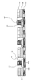
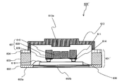
- FIG. 1A When a sensor upper cap is abbreviate
- FIG. 1A and 1B are cross-sectional views showing the overall configuration of a sensor device according to Embodiment 1 of the present invention.
- the case of packaging the control IC together with the acceleration sensor will be described, but the present invention is not limited to this, and only the sensor may be packaged.
- FIG. 1A is a cross-sectional view of the acceleration sensor device 100 when a flat substrate (hereinafter referred to as a normal substrate) is used, and FIG. 1B is for cutting in advance the substrate to be used and storing part or all of the sensor and control IC. It is sectional drawing of acceleration sensor device 100 'at the time of using the board
- control IC is not only used to control the sensor.
- the control IC may process the signal obtained from the sensor, such as amplifying the signal from the sensor.
- the control IC may include processing other than processing of the signal output from the sensor. For this reason, it may be simply described as “IC” instead of "control IC”.
- an acceleration sensor device 100 using a normal substrate includes a substrate 101, a through electrode 105, a control IC 106, a sensor 107, wires 114 and 115, a sensor upper cap (control cap) 112, and a package cap 113. .
- the substrate 101 is a substrate containing an organic material and having a wiring.
- the substrate 101 includes a first substrate 102 having a portion 102a containing a conductive material and a portion 102b containing an insulating material, a second substrate 103 containing an insulating material and disposed on the first substrate 102, and an insulating material. It is formed by three layers including the third substrate 104 disposed on the second substrate 103.
- the conductive material is a metal or the like, and for example, copper, silver, gold, nickel, palladium or the like can be used.
- An insulating resin is used as the insulating material.
- epoxy resin for example, epoxy resin, polyimide resin, benzocyclobutene resin, polyamide, phenol resin, silicone resin, fluorine resin, liquid crystal polymer, polyamide imide, polybenzoxazole, cyanate resin, aramid, polyolefin, polyester, BT resin, FR-4, FR-5, polyacetal, polybutylene terephthalate, syndiotactic polystyrene, polyphenylene sulfide, polyetheretherketone, polyether nitrile, polycarbonate, polyphenylene ether polysulfone, polyether sulfone, polyarylate, polyether imide, etc.
- the above resins may be used alone or in combination of two or more resins.
- an inorganic filler such as glass, talc, mica, silica, alumina, etc. may be used in combination with the above-mentioned resin.
- an inorganic filler such as glass, talc, mica, silica, alumina, etc.
- the substrate 101 may be three or less, or three or more.
- the sensor 107 is disposed on the weight portion 110, the flexible portion 109 connected to the weight portion 110, the support portion 108 connected to the flexible portion 109, and the flexible portion 109, thereby displacing the flexible portion 109. It includes a plurality of piezoresistive elements (not shown) that detect in three axial directions of XYZ, and an electrode 111.
- the weight portion 110 is displaced, and in accordance with this displacement, the flexible portion 109 is bent.
- a force is applied to the piezoresistive element disposed in the flexible portion 109, and the resistance value of the piezoresistive element changes.
- the change in the resistance value is detected to detect the magnitude, direction, and the like of the acceleration applied to the sensor 107.
- a signal from the sensor 107 is transmitted from the electrode 111 to the control IC 106 through the wiring 115, and a signal from the control IC 106 is transmitted to the outside of the substrate 101 through the wiring 114, the through electrode 105, and the like.
- the sensor upper cap 112 restricts excessive displacement in the upward direction of the weight portion 110 and the flexible portion 109 to prevent damage.
- the sensor top cap 112 may be omitted, and the package cap 113 may play the same role as the sensor top cap 112 if the sensor top cap 112 is omitted.
- a convex stopper 113a may be formed on a portion of the package cap 113 corresponding to the sensor 107.
- the package cap 113 of the acceleration sensor device 100 illustrated in FIG. 1A contains an organic material, and an insulating resin such as an epoxy resin, an acrylic resin, or a polyimide resin is used.
- an insulating resin such as an epoxy resin, an acrylic resin, or a polyimide resin is used.
- the sensor 107 is not sealed with resin, and the inside of the package cap 113 is hollow.
- the sensor 107, the control IC 106, and the substrate 101 according to the present embodiment illustrated in FIG. 1A are covered and packaged by the package cap 113 containing an organic material.
- the inside of the package cap 113 is hollow.
- Sex is high.
- the value of the thermal expansion coefficient of the package cap 113 and the value of the thermal expansion coefficient of the substrate 101 are substantially the same, and the difference between the thermal expansion coefficients of the two is within ⁇ 3 ppm.
- the adhesive for bonding the substrate 101 and the package cap 113 is preferably a resin having a thermal expansion coefficient close to that of the substrate 101 and the package cap 113.
- the connection relationship of the wiring in accordance with the change of the specification of the control IC 106, that is, when changing the layout of the pin connect connecting the control IC 106 and the sensor 107, the design of the wiring pattern, etc. Because a printed circuit board can be used, the cost of modification can be reduced compared to using a ceramic package or an alumina package. Furthermore, in the case of a ceramic package, it is difficult to reduce the height because thinning the package itself may cause cracks.
- an organic material for example, an insulating resin
- the package cap 113 and the substrate 101 so the weight is lighter and the mechanical shock and vibration resistance are excellent compared to ceramic packages and alumina packages. It is possible to make it tall. Thereby, for example, application to small terminals such as portable electronic devices becomes possible.
- the inside of the acceleration sensor device 100 according to the present embodiment is hollow without being resin-sealed, so there is a possibility that the resin may enter into the gap of the weight portion 110 of the sensor 107 or the like. Absent.
- the inside of the acceleration sensor device 100 is hollow without being resin-sealed, stress is not applied to the sensor 107, and there is no possibility that the offset value of the sensor 107 may be shifted. Therefore, the reliability of the performance of the acceleration sensor device 100 is maintained.
- an acceleration sensor device 100 'using a cavity substrate will be described.
- the same or similar components as or to those of the acceleration sensor device 100 in the case where the normal substrate shown in FIG. 1A is used will be assigned the same reference numerals, and overlapping descriptions will be omitted.
- an acceleration sensor device 100 'in the case of using a cavity substrate is similar to the acceleration sensor device 100 shown in FIG. 1A, including a substrate 101' containing an organic material, a through electrode 105, a control IC 106, and a weight.
- the flexible portion 109 connected to the portion 110 and the weight portion 110 and the support portion 108 connected to the flexible portion 109 and the flexible portion 109 are arranged to detect the displacement of the flexible portion 109 in the three axial directions of XYZ. It includes a sensor 107 including a plurality of piezoresistive elements (not shown) and electrodes 111, wires 114, 115, 116, a sensor upper cap 112, and a package cap 113 including an organic material.
- the substrate 101 ′ includes a first substrate 102 having a portion 102a containing a conductive material and a portion 102b containing an insulating material, a second substrate 103 containing an insulating material, and a third substrate 104 containing an insulating material. It is formed by two layers. However, the present invention is not limited to this, and the number of layers of the substrate 101 ′ may be three or less, or three or more.
- the conductive material or insulating material used for the first substrate 102, the second substrate 103, and the third substrate 104 is the conductive material used for the first substrate 102, the second substrate 103, and the third substrate 104 shown in FIG. 1A. Or similar to the insulating material.
- the sensor upper cap 112 may be omitted. If the sensor top cap 112 is omitted, the package cap 113 may play the same role as the sensor top cap 112. When the package cap 113 plays the same role as the sensor upper cap 112, as shown in FIG. 10B, a convex stopper 113a may be formed on a portion of the package cap 113 corresponding to the sensor 107.
- the package using the substrate (cavity substrate) in which a space (cavity) capable of storing a part or the whole of the control IC 106 and the sensor 107 is formed is more than the package using the normal substrate. It is possible to lower the overall height.
- the operation of the acceleration sensor device 100 'using the cavity substrate 101' is the same as that of the acceleration sensor device 100 using the normal substrate 101 shown in FIG. 1A, and thus the description thereof is omitted here.
- the sensor 107, the control IC 106, and the substrate 101 'illustrated in FIG. 1B are packaged by being covered with a package cap 113 that includes an organic material and is, for example, an insulating resin.
- the inside of the package cap 113 is hollow.
- the value of the thermal expansion coefficient of the substrate 101 ′ and the value of the thermal expansion coefficient of the package cap 113 are substantially the same, and the difference between the thermal expansion coefficients of the two is within ⁇ 3 ppm.
- the adhesive for bonding the substrate 101 ′ and the package cap 113 is preferably a resin having a thermal expansion coefficient close to that of the substrate 101 ′ and the package cap 113.
- the connection relationship is changed in accordance with the change of the specification of the control IC, etc. (that is, when the design of the arrangement and wiring pattern of the pin connect connecting the control IC 106 and the sensor 107 is changed) Since a printed circuit board can be used as', the cost of modification can be reduced compared to the case of using a ceramic package or an alumina package.
- the inside of the acceleration sensor device 100 'according to the present embodiment is hollow without being resin-sealed, so that the resin gets into gaps such as the weight portion of the sensor 107. There is no fear. Furthermore, since the inside of the acceleration sensor device 100 is hollow without being resin-sealed, stress is not applied to the sensor 107, and there is no possibility that the offset value of the sensor 107 may be shifted. Therefore, the reliability of the performance of the acceleration sensor device 100 'is maintained.
- a concave-shaped space (cavity) is formed in advance, in which the substrate to be used is cut and the sensor 107 is accommodated. Therefore, the package 113 of the acceleration sensor device 100 'can be further reduced in height than the package of the acceleration sensor device 100 using the normal substrate 100 shown in FIG. 1A. Further, in order to cut the substrate in advance and expose the lower layer such as the first substrate 102, the first substrate 102 and the control IC 106 are directly connected by the wiring 114 without the intervention of the through electrode.
- the depth of the recess (cavity) formed in the substrate is preferably 500 ⁇ m or less, and more preferably 100 ⁇ m to 500 ⁇ m.
- the depth of the cavity is larger than 500 ⁇ m, the capillary interferes with the substrate or the sensor at the time of wire bonding, and the workability is lowered. In addition, if the depth of the cavity is 100 ⁇ m or more, a reduction in height can be expected, and the workability at the time of wire bonding can be maintained.
- the electrode 111 of the sensor 107 and the third substrate 104 are connected by the wiring 116, and the connection portion of the wiring 116 of the third substrate 104 is further connected to the third wiring 104 via the through electrode 105.
- Wiring can be formed at the connection portion of the one substrate 102 to connect the sensor 107 and the control IC 106.
- the degree of freedom in connection between the sensor 107 and the control IC 106 can be increased.
- FIGS. 2 to 5 A method of manufacturing the acceleration sensor device 100 'using the cavity substrate shown in FIG. 1B will be described with reference to FIGS.
- FIGS. 2 to 5 the same or similar components as or to those of the acceleration sensor device 100 ′ in the case of using the cavity substrate shown in FIG.
- packaging the control IC 106 together with the acceleration sensor 107 will be described, but the present invention is not limited to this, and only the sensor may be packaged.
- the sensor 107 as shown in FIG. 1B, a substrate 101 ' including the first substrate 102, the second substrate 103 and the third substrate 104, the control IC 106, and the package cap 113 are manufactured.
- the substrate 101 ′ as shown in FIG. 2, the substrate 101 is etched using a laser or the like to form a cavity. It is also possible to form a plurality of cavities in one substrate 101 'as illustrated in FIG. 1B. Naturally, it is also possible to form one cavity in one substrate 101 '.
- the control IC 106 and the sensor 107 are adhered on the substrate 101 'in a cavity by die attach (die bonding) or the like.
- electrical connection between the substrate 101 ′, the control IC 106, and the sensor 107 is made by wires 114, 115, 116 such as wire bonding and through electrodes (not shown, refer to 105 in FIG. 1B).
- the package cap 113 set in the mold 501 is adhered and sealed on the substrate 101 ′ so as to cover the sensor 107.
- the mold 501 in which the package cap 113 is set is removed.
- the substrate 101 ' is diced and separated into individual pieces by separating the individual acceleration sensor devices.
- an acceleration sensor device 100 'as shown in FIG. 1B is obtained.
- the package cap 113 contains an organic material, and can be formed of, for example, an insulating resin. Therefore, the plurality of package caps 113 can be formed on one side of the mold 501 which is a flat plate of metal (for example, copper) having a plurality of openings, with a portion thereof being fitted and set in the openings. . Then, an adhesive is applied to the package cap 113 if necessary, and the mold 501 is placed on the upper surface of the substrate 101 'in FIG. It can be glued to The adhesive used here is preferably a resin having a thermal expansion coefficient close to that of the substrate 101 ′ and the package cap 113. Thereafter, the mold 501 can be removed.
- the mold 501 is preferably a resin having a thermal expansion coefficient close to that of the substrate 101 ′ and the package cap 113.
- the space between the package cap 113 and the substrate 101 ', the control IC 106, and the sensor 107 is hollow (a gap is left), and the substrate 101', the control IC 106, and the sensor 107 are not resin-sealed. There is no need to create a barrier to prevent the flow of resin into. Therefore, it is possible to further shorten the manufacturing process.
- the method of manufacturing the acceleration sensor device 100 'using the cavity substrate shown in FIG. 1B has been described above with reference to FIGS. 2 to 5, the method of manufacturing the acceleration sensor device 100 described in FIG. It can be described in substantially the same manner as the method of manufacturing the acceleration sensor device 100 '.
- the acceleration sensor device 100 described in FIG. 1A normally uses a substrate, the flat substrate 101 in which the sensor storage space is not formed is prepared.
- acceleration sensor device 100 using the cavity board
- this invention is not limited to this, According to the mounting method of each device, arrangement, etc. suitably It may be changed.
- FIGS. 6A and 6B are cross-sectional views showing the overall configuration of an acceleration sensor device according to Embodiment 2 of the present invention.
- FIG. 6A is a cross-sectional view of a flip chip (Flip Chip) mounted acceleration sensor device 600 when a normal substrate is used
- FIG. 6B is for cutting in advance the substrate to be used and storing part or all of the sensor and control IC. It is sectional drawing of acceleration sensor device 600 'of flip chip mounting at the time of using the cavity board
- flip chip flip chip
- an acceleration sensor device 600 using a normal substrate includes a substrate 601, a control IC 606, a sensor 607, an electrode 611, a sensor upper cap 612, a package cap 613, a bump 614, and a wire 615.
- the substrate 601 is a substrate containing an organic material and having a wiring.
- the substrate 601 includes, for example, a first substrate 602 having a portion 602a containing a conductive material and a portion 602b containing an insulating material, a second substrate 603 containing an insulating material and disposed on the first substrate 602, and an insulating material. It is formed by three layers including the third substrate 604 disposed on the second substrate 603.
- the conductive material or the insulating material contained in the first substrate 602, the second substrate 603, and the third substrate 604 is the same as that described in Embodiment 1. In this embodiment, an example in which the substrate 601 includes three layers will be described. However, the present invention is not limited to this, and the number of layers of the substrate 601 may be three or less, or three or more.
- the sensor 607 is disposed on the weight portion 610, the flexible portion 609 connected to the weight portion 610, the support portion 608 connected to the flexible portion 609, and the flexible portion 609 to displace the flexible portion 609. It includes a plurality of piezoresistive elements (not shown) that detect in three axial directions of XYZ, and an electrode 611. Similar to the acceleration sensor described in the first embodiment, when acceleration is applied to the sensor 607, the weight portion 610 is displaced, and the flexible portion 609 is bent along with this displacement. When the flexible portion 609 bends, a force is applied to the piezoresistive element disposed in the flexible portion 609, and the resistance value of the piezoresistive element changes.
- the change in the resistance value is detected to detect the magnitude, direction, and the like of the acceleration applied to the acceleration sensor device 600.
- a signal from the sensor 607 is transmitted from the electrode 611 to the control IC 606, and a signal from the control IC 606 is transmitted to the substrate 601 through the wiring 615 and the through electrode 605.
- the sensor upper cap 612 restricts excessive displacement in the upward direction of the weight portion 610 and the flexible portion 609 to prevent breakage and the like.
- the sensor top cap 612 may be omitted, in which case the package cap 613 may play the same role as the sensor top cap 612. If the package cap 613 plays the same role as the sensor upper cap 612, as shown in FIG.
- a stopper 613a may be formed on a portion of the package cap 613 corresponding to the sensor 607.
- the stopper 613a may have a convex shape, but is not limited thereto.
- the height of the package cap 613 may be reduced to bring the portion of the package cap 613 corresponding to the sensor 607 closer to the movable portion of the sensor.
- the sensor 607 and the control IC 606 are flip chip mounted and connected via bumps 614. Therefore, it is not necessary to use a wire for connection between the sensor 607 and the control IC 606. If the wiring is not used to connect the sensor 607 and the control IC 606, the mounting area can be reduced, and the entire package of the acceleration sensor device 600 can be further miniaturized.
- the package cap 613 of the acceleration sensor 600 illustrated in FIG. 6A includes an organic material, and for example, an insulating resin is used.
- the inside of the package cap 613 is not sealed with resin but is hollow. Therefore, when a substrate containing an organic material is used as the substrate 601, the value of the thermal expansion coefficient of the substrate 601 and the value of the thermal expansion coefficient of the package cap 613 are close to each other.
- the reliability of the The value of the thermal expansion coefficient of the substrate 601 and the value of the thermal expansion coefficient of the package cap 613 are substantially the same, and the difference between the thermal expansion coefficients of the two is within ⁇ 3 ppm.
- the adhesive for bonding the substrate 601 and the package cap 613 is preferably a resin having a thermal expansion coefficient close to that of the substrate 601 and the package cap 613.
- the connection relationship is changed in accordance with the change of the specification of the control IC 606 (that is, when the design of the arrangement and wiring pattern of the pin connect connecting the control IC 606 and the sensor 607 is changed)
- the manufacturing cost can be reduced compared to a ceramic package or an alumina package.
- an organic material, such as an insulating resin for the package cap 613 and the substrate 601
- the mechanical shock resistance and vibration resistance are increased, and the height of the package itself can be reduced.
- the inside of the acceleration sensor device 600 is in a hollow state, there is no possibility that resin may enter the gap between the sensor 607 and the control IC 606. Furthermore, since the inside of the acceleration sensor device 600 is hollow without being resin-sealed, stress is not applied to the sensor 607, and there is no possibility that the offset value of the sensor 607 may be shifted. Therefore, the reliability of the performance of the acceleration sensor device 600 is maintained.
- FIG. 6B shows a flip chip mounted acceleration sensor device 600 'when using a cavity substrate.
- a cavity substrate having a space in which the sensor is housed, it is generally possible to make the whole package thinner than when using a substrate normally.
- the same or similar components as or to those of the acceleration sensor device 600 in the case of using the normal substrate shown in FIG. 6A will be assigned the same reference numerals, and overlapping descriptions will be omitted.
- a flip chip mounting acceleration sensor 600 ' is similar to the acceleration sensor device 600 shown in FIG. 6A, including a substrate 601' containing an organic material, a control IC 606, and a weight portion.
- a sensor upper cap 612, a package 613 containing an organic material, a bump 614, and a wire 616 is similar to the acceleration sensor device 600 shown in FIG. 6A, including a substrate 601' containing an organic material, a control IC 606, and a weight portion.
- the substrate 601 ′ includes three layers including a first substrate 602 having a portion 602a containing a conductive material and a portion 602b containing an insulating material, a second substrate 603 containing an insulating material, and a third substrate 604 containing an insulating material. It is formed by However, the present invention is not limited to this, and the number of layers of the substrate 601 ′ may be three or less, or three or more.
- the conductive material or insulating material used for the first substrate 602, the second substrate 603, and the third substrate 604 is the conductive material used for the first substrate 602, the second substrate 603, and the third substrate 604 shown in FIG. 6A. Or similar to the insulating material. Also, the sensor upper cap 612 may be omitted.
- the package cap 613 may play the same role as the sensor upper cap 612. If the package cap 613 plays the same role as the sensor upper cap 612, as shown in FIG. 11B, the stopper 613a may be formed on a portion of the package cap 613 corresponding to the sensor 607. The stopper 613a may have a convex shape, but is not limited thereto. When the package cap 613 plays the same role as the sensor upper cap 612, the height of the package cap 613 may be reduced to bring the portion of the package cap 613 corresponding to the sensor 607 closer to the movable portion of the sensor.
- the operation of the acceleration sensor device 600 'using the cavity substrate 601 is the same as that of the acceleration sensor device 600 using the normal substrate 601' shown in FIG.
- the package cap 613 of the acceleration sensor device 600 ′ shown in FIG. 6B contains an organic material, and for example, an insulating resin is used.
- the inside of the package cap 613 is not sealed with resin and is hollow. Therefore, when a substrate containing an organic material is used as the substrate 601 ′, the value of the thermal expansion coefficient of the substrate 601 ′ and the value of the thermal expansion coefficient of the package cap 613 are close to each other. The reliability of bonding is high.
- the value of the thermal expansion coefficient of the substrate 601 ′ and the value of the thermal expansion coefficient of the package cap 613 are substantially the same, and the difference between the thermal expansion coefficients of the two is within ⁇ 3 ppm.
- the adhesive for bonding the substrate 601 ′ and the package cap 613 is preferably a resin having a thermal expansion coefficient close to that of the substrate 601 ′ and the package cap 613.
- a printed board is used for the board 601 '. Manufacturing costs are reduced compared to ceramic packages and alumina packages.
- the mechanical shock resistance and vibration resistance are increased, and the height of the package itself can be reduced.
- the inside of the acceleration sensor device 600 ' is hollow, there is no possibility that resin may enter the gap between the sensor 607 and the control IC 606. Furthermore, since the inside of the acceleration sensor device 600 'is hollow without being resin-sealed, stress is not applied to the sensor 607, and there is no possibility that the offset value of the sensor 607 may be shifted. Therefore, the reliability of the performance of the acceleration sensor device 600 'is maintained.
- the sensor 607 of the acceleration sensor device 600 ′ and the control IC 606 are flip chip mounted, and are connected via the bumps 614. Since it is not necessary to use a wire for connection between the sensor 607 and the control IC 606, the mounting area can be reduced, and the entire package of the acceleration sensor device 600 'can be miniaturized.
- the package 613 of the acceleration sensor device 600 ′ is generally the one shown in FIG. 6A because the cavity substrate 601 ′ has a concave space (cavity) for cutting the substrate to be used and housing the sensor 607 in advance. It is possible to further reduce the height of the package of the acceleration sensor device 600 using the substrate 600.
- the depth of the recess (cavity) formed in the substrate is preferably 500 ⁇ m or less, and more preferably 100 ⁇ m to 500 ⁇ m. If the depth of the cavity is larger than 500 ⁇ m, the capillary interferes with the substrate or the sensor at the time of wire bonding, and the workability is lowered. In addition, if the depth of the cavity is 100 ⁇ m or more, a reduction in height can be expected, and the workability at the time of wire bonding can be maintained.
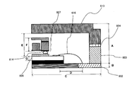
- FIG. 7 is a part of a cross-sectional view of a flip chip mounted acceleration sensor device when a cavity substrate is used. Components similar to the flip chip mounted acceleration sensor device 600 ′ illustrated in FIG. 6B are given the same reference numerals as in FIG. 6B.
- FIG. 7 for example, it is designed to be A1.15 mm, B0.1 mm, C1.6 mm, D0.17 mm, E0.7 mm, F0.5 mm, G0.1 mm.
- B0.1 mm B0.1 mm
- C1.6 mm D0.17 mm
- E0.7 mm E0.7 mm
- F0.5 mm G0.1 mm
- G0.1 mm G0.1 mm
- an acceleration sensor device according to the third embodiment will be described with reference to FIGS. 12 to 14.
- the case of packaging the control IC together with the acceleration sensor will be described, but the present invention is not limited to this, and only the sensor may be packaged.
- the acceleration sensor device according to the third embodiment has the same configuration as the acceleration sensor device 100 'according to the first embodiment except for the first substrate of the acceleration sensor device 100' using the cavity substrate according to the first embodiment. Have. Therefore, the same reference numerals are given to the same components or similar components as those of the acceleration sensor device 100 'shown in FIG. 1B, and the redundant description will be omitted.
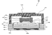
- FIG. 12 is a cross-sectional view showing an entire configuration of an acceleration sensor device according to a third embodiment of the present invention.
- FIG. 12 is a cross-sectional view of the acceleration sensor device 200 when a cavity substrate is used and a first substrate 102 ', which is a metal substrate, is disposed in the lowermost layer of the substrate 201, which is a multilayer substrate.
- the acceleration sensor device 200 according to the third embodiment shown in FIG. 12 has the same configuration as the acceleration sensor device 100 ′ according to the first embodiment except for the multilayer substrate 201 used in the acceleration sensor device 200. doing. Therefore, the same reference numerals are given to the same components or similar components as those of the acceleration sensor device 100 'shown in FIG. 1B, and the redundant description will be omitted.
- the acceleration sensor device 200 includes the multilayer substrate 201, the control IC 106, the sensor 107, the electrode 111, the sensor upper cap 112, the sensor lower cap 210, the insulating layer 206, the package cap 113, the electrode 205, the wiring 115, and Wiring 116 is included.
- the multilayer substrate 201 is a cavity substrate in which a recessed storage space (cavity) 202 is formed, and the package inside of the acceleration sensor device 200 is hollow.
- the multilayer substrate 201 includes a first substrate 102 'which is a metal substrate, a second substrate 103 disposed on the first substrate 102 and containing an insulating material, and a third substrate disposed on the second substrate 103 and containing a conductive material. It is formed of five layers including a substrate 204, an insulating layer 203 covering a part of the first substrate 102 ', and an insulating layer 206 covering a part of the third substrate 204.
- the conductive substance contained in the third substrate 204 is a metal or the like, and for example, copper, silver, gold, nickel, palladium or the like can be used.
- An insulating resin is used for the insulating material contained in the second substrate 103.
- epoxy resin for example, epoxy resin, polyimide resin, benzocyclobutene resin, polyamide, phenol resin, silicone resin, fluorine resin, liquid crystal polymer, polyamide imide, polybenzoxazole, cyanate resin, aramid, polyolefin, polyester, BT resin, FR-4, FR-5, polyacetal, polybutylene terephthalate, syndiotactic polystyrene, polyphenylene sulfide, polyetheretherketone, polyether nitrile, polycarbonate, polyphenylene ether polysulfone, polyether sulfone, polyarylate, polyether imide, etc.
- the above resins may be used alone or in combination of two or more resins.
- the multilayer substrate 201 includes a metal 2 layer formed of a first substrate 102 ′ and a third substrate 204.
- the present invention is not limited to this, and the layers of the substrate 201 may be five layers or less including two metal layers, or five layers or more including two metal layers.
- the recess (cavity) 202 for housing the control IC 106 and the sensor 107 is formed by etching, laser processing, or the like. In FIG.
- the second substrate 103 is completely cavity processed, and the third substrate 204 is patterned. Furthermore, in the acceleration device 200 according to the third embodiment of the present invention shown in FIG. 12, a recess (cavity) 202 is formed such that the first substrate 102 ′ is at the bottom. The first substrate 102 ′ is patterned, and the first substrate 102 ′ a corresponding to the recess (cavity) 202 formed in the multilayer wiring substrate 201 is covered with the insulating layer 203.
- the first substrate 102 ' may include a metal having high thermal conductivity, such as copper, but is not limited thereto.
- the thickness of the first substrate 102 ' is preferably 15 ⁇ m to 80 ⁇ m in consideration of the strength of the package of the acceleration sensor device 200.
- the control IC 106 is mounted and disposed on the first substrate 102 ′ a corresponding to the recess (cavity) 202 formed in the multilayer wiring substrate 201 by an adhesive.
- the third substrate 204 and the first substrate 102 ′ b not corresponding to the recess 202 formed in the multilayer wiring substrate 201 may function as an electrode pad or an external connection pad.
- the insulating layer 203 contains an insulating resin such as an organic material, and for example, an epoxy resin, a polyimide resin, a benzocyclobutene resin, a polyamide, a phenol resin, a silicone resin, a fluorine resin, a liquid crystal polymer, a polyamide imide, a polybenzoxazole, a cyanate Resin, aramid, polyolefin, polyester, BT resin, FR-4, FR-5, polyacetal, polybutylene terephthalate, syndiotactic polystyrene, polyphenylene sulfide, polyether ether ketone, polyether nitrile, polycarbonate, polyphenylene ether polysulfone, poly Ether sulfone, polyarylate, polyether imide and the like can be used.
- the above resins may be used alone or in combination of two or more resins.
- an inorganic filler such as glass, talc, mica,
- the sensor 107 is disposed on the weight portion 110, the flexible portion 109 connected to the weight portion 110, the support portion 108 connected to the flexible portion 109, and the flexible portion 109, thereby displacing the flexible portion 109. It includes a plurality of piezoresistive elements (not shown) that detect in three axial directions of XYZ, and an electrode 111. Similar to the acceleration sensor described in the first embodiment, when acceleration is applied to the sensor 107, the weight portion 110 is displaced, and the flexible portion 109 is bent in accordance with this displacement. When the flexible portion 109 bends, a force is applied to the piezoresistive element disposed in the flexible portion 109, and the resistance value of the piezoresistive element changes.
- the change in the resistance value is detected to detect the magnitude, direction, and the like of the acceleration applied to the acceleration sensor device 200.
- a signal from the sensor 107 is transmitted from the electrode 111 to the control IC 106 through the wiring 115, and a signal from the control IC 106 is transmitted through the electrode 205, the wiring 116, the third substrate 204, the through electrode 105, and the first substrate 102'b. Is transmitted to the outside.
- Each wire and each electrode may be potted with an insulating resin.
- the sensor upper cap 112 limits excessive displacement in the upward direction of the weight portion 110 and the flexible portion 109, and prevents damage or the like.
- the sensor lower cap 210 keeps the air tightness in the sensor 107 and limits excessive downward movement of the weight portion 110.
- the sensor upper cap 112 and the sensor lower cap 210 may be omitted, and in this case, as shown in FIG. 10B, a convex stopper is provided in a portion corresponding to the sensor of the package cap 113. May play the same role as the sensor upper cap 112. Also, the control IC 106 may play the same role as the sensor lower cap 210.
- the insulating layer 206 is disposed between the third substrate 204 and the package cap 113 as a cover layer.
- the insulating layer 206 contains an insulating resin such as an organic material, and for example, an epoxy resin, a polyimide resin, a benzocyclobutene resin, a polyamide, a phenol resin, a silicone resin, a fluorine resin, a liquid crystal polymer, a polyamide imide, a polybenzoxazole, a cyanate Resin, aramid, polyolefin, polyester, BT resin, FR-4, FR-5, polyacetal, polybutylene terephthalate, syndiotactic polystyrene, polyphenylene sulfide, polyether ether ketone, polyether nitrile, polycarbonate, polyphenylene ether polysulfone, poly Ether sulfone, polyarylate, polyether imide and the like can be used.
- the above resins may be
- FIG. 13 (a) is a plan view of a part of the package of the acceleration sensor device 200 shown in FIG. 12 as seen from the bottom, and FIG. 13 (b) is taken along cc in FIG. 13 (a). It is a sectional view seen from '. 13A and 13B, the insulating layer 203, the first substrate 102 ', the second substrate 103, the third substrate 204, the concave portion (cavity) 202, the control IC 106, the through electrode 105, and the insulating layer 206.
- the configuration of the acceleration sensor device 200 other than the above is omitted.
- the dummy pad 209 is disposed on the surface of the insulating layer 203, the dummy pad 209 may be omitted.
- the control IC 106 is disposed directly on the first substrate 102 '.
- the entire package of the acceleration sensor device 200 also has a low height. It is possible. Furthermore, since the first substrate 102 'that is a metal substrate is used for the multilayer substrate 201, the strength of the entire package of the acceleration sensor device 200 is improved even when the cavity formed in the multilayer substrate 201 is deep. , Warpage is reduced.
- the control IC 106 is mounted on the first substrate 102 ′ by an adhesive, for example, when the first substrate 102 ′ includes copper, the thermal expansion coefficient of copper is (17.5 ppm / ° C.) Since the thermal expansion coefficient (about 20 ppm / ° C.) of the resin is closer to the thermal expansion coefficient (3.3 ppm / ° C.) of silicon used for the control IC 106, stress at high temperature and low temperature is reduced.
- the control IC 106 and the sensor 107 have the effect of dissipating the heat of the
- FIG. 14 an opening 202 'is provided in a multilayer substrate 201', and a metal substrate 217 containing a substance excellent in thermal conductivity is disposed to close the opening 202 'of the multilayer substrate 201'.
- FIG. 217 is a cross-sectional view of the acceleration sensor device 200 ′ in the case of forming a concave storage space (concave portion).
- the acceleration sensor device 200 ′ includes a multilayer substrate 201 ′ having an opening 202 ′, a metal substrate 217 closing the opening 202 ′ of the multilayer substrate 201 ′, an insulating layer 203 covering the metal substrate 217, a control IC 106, and a sensor 107, an electrode 111, a sensor upper cap 112, an insulating layer 206, a package cap 113, an electrode 205, a wire 115, and a wire 116.
- the interior of the package of the acceleration sensor device 200 'described in FIG. 14 is hollow.
- the multilayer substrate 201 ′ includes a first substrate 208 including a conductive material, a second substrate 103 including an insulating material, a third substrate 204 including a conductive material, and an insulating layer 206 covering a portion of the third substrate.
- the conductive substance contained in the first substrate 208 and the third substrate 204 is a metal or the like, and for example, copper, silver, gold, nickel, palladium, or the like can be used.
- An insulating resin is used for the insulating material contained in the second substrate 103.
- epoxy resin for example, epoxy resin, polyimide resin, benzocyclobutene resin, polyamide, phenol resin, silicone resin, fluorine resin, liquid crystal polymer, polyamide imide, polybenzoxazole, cyanate resin, aramid, polyolefin, polyester, BT resin, FR-4, FR-5, polyacetal, polybutylene terephthalate, syndiotactic polystyrene, polyphenylene sulfide, polyetheretherketone, polyether nitrile, polycarbonate, polyphenylene ether polysulfone, polyether sulfone, polyarylate, polyether imide, etc.
- the above resins may be used alone or in combination of two or more resins.
- the multilayer substrate 201 includes four layers including a metal 2 layer formed of the first substrate 208 and the third substrate 204, a second substrate 103, and the insulating layer 206.
- the present invention is not limited thereto, and the layers of the substrate 201 may be four or less including two metal layers, or four or more layers including two metal layers.
- the multilayer substrate 201 ′ has the opening 202 ′, and the metal substrate 217 is disposed to close the opening 202 ′.
- the metal substrate 217 is disposed so as to close the opening 202 ′ provided in the multilayer substrate 201 ′, and the surface side facing the surface facing the opening 202 ′ of the multilayer substrate 201 ′ is covered with the insulating layer 203. As shown in FIG. 14, a multi-layer substrate 201 ′ and a metal substrate 217 form a concave storage space (recess), and the metal substrate in the opening 202 ′ of the multi-layer substrate 201 ′ closed by the metal substrate 217.
- the control IC 106 is disposed on the circuit 217.
- the metal substrate 217 includes a metal having excellent thermal conductivity, and may include, for example, copper, but is not limited thereto.
- the thickness of the metal substrate 217 is preferably 15 ⁇ m to 80 ⁇ m in consideration of the strength of the package.
- the control IC 106 is mounted and arranged on the metal substrate 217 by an adhesive.
- the configuration of the acceleration sensor device 200 other than the multilayer substrate 201 ′ and the metal substrate 217 is the same as the configuration of the acceleration sensor device 200 shown in FIG. 12, and thus the detailed description will be omitted.
- the control IC 106 is mounted on the metal substrate 217 by the adhesive, when the metal substrate 217 contains copper, the thermal expansion coefficient of copper is (17.5 ppm / ° C.), and the thermal expansion coefficient of the resin is Because it is closer to the thermal expansion coefficient (3.3 ppm / ° C.) of silicon used for the control IC 106 than (about 20 ppm / ° C.), stress at high temperature and low temperature is reduced. Furthermore, since the metal substrate 217 is a metal substrate containing a metal having a thermal conductivity higher than that of the insulating material used for the portion 102 b of the first substrate 102 described in the first embodiment, heat generation from the control IC 106 and the sensor 107 Have the effect of radiating heat.
- FIG. 8A is a cross-sectional view of the acceleration sensor device 800 when the control IC 106 and the sensor 107 are arranged side by side on the substrate 101 using the normal substrate shown in FIG. 1A.
- FIG. 8A is a cross-sectional view of the acceleration sensor device 800 when the control IC 106 and the sensor 107 are arranged side by side on the substrate 101 using the normal substrate shown in FIG. 1A.
- FIG. 8B is a cross-sectional view of the acceleration sensor device 800 ′ when the control IC 106 and the sensor 107 are arranged side by side on the substrate 101 ′ using the cavity substrate shown in FIG. 1B.
- the control IC 106 and the sensor 107 may be arranged side by side on the substrate 101 or 101 ′, necessary wiring and the like may be performed, covered by a package cap 113, and packaging may be performed.
- the control IC 106 and the sensor 107 may be covered by the same package cap 113 as shown, or may be covered by separate package caps although not shown.
- the package cap 113 includes an organic material having a thermal expansion coefficient value close to or substantially the same as the thermal expansion coefficient value of the substrate 101 or 101 'as in the first embodiment and the second embodiment, and the inside of the sensor device is hollow. It is a state.
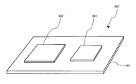
- FIGS. 9A and 9B show a semiconductor device using the acceleration sensor device of any of Embodiments 1 to 3, and for example, show an example of sensor modules 900 and 900 '.
- the sensor modules 900 and 900 ' are used, for example, in mobile phones, PDAs, and the like.
- a semiconductor device refers to any device that can function using semiconductor technology, and electronic components and electronic devices are included in the scope of the semiconductor device.
- FIG. 9A shows a sensor module 900 using an acceleration sensor device.
- the sensor module 900 includes a mounting substrate 901 and a sensor chip 902.
- the sensor chip 902 includes an organic material shown in FIG. 1A or FIG. 1B, or FIG. 6A or FIG. 6B, or FIG. 8A or FIG. It includes a sensor device including a sensor and a control IC covered by a package made of an insulating resin.
- the mounting substrate 901 is a substrate made of an organic material, and is made of, for example, an insulating resin. Wiring (not shown) for electrically connecting to the wiring of the sensor chip 902 is formed on the top surface of the mounting substrate 901. As shown in FIG. 9A, when the sensor chip 902 is mounted on the mounting substrate 901, unlike the sensor chip using the conventional ceramic package, the value of the thermal expansion coefficient of the mounting substrate 901 and the thermal expansion of the package of the sensor chip 902 Since the values of the coefficients are close, the reliability of the connection between the mounting substrate 901 and the package of the sensor chip 902 is high, which is advantageous for large package, thin package, and narrow gap mounting.
- the value of the thermal expansion coefficient of the mounting substrate 901 and the value of the thermal expansion coefficient of the package of the sensor chip 902 are substantially the same, and the difference between the thermal expansion coefficients of the two is within ⁇ 3 ppm.
- the adhesive for bonding the mounting substrate 901 and the package of the sensor chip 902 is preferably a resin having a thermal expansion coefficient close to that of the package of the mounting substrate 901 and the package of the sensor chip 902.
- the present invention is not limited to this, and the mounting substrate 901 and the package of the sensor chip 902 may be connected via a bump.
- FIG. 9B shows a sensor module 900 'using a signal processing chip including a sensor chip and a control IC. Components similar to those in FIG. 9A are assigned the same reference numerals, and redundant descriptions are omitted.
- the sensor module 900 ′ includes a mounting substrate 901, a sensor chip 902 ′, and a signal processing chip 903 including a control IC.
- the mounting substrate 901 is similar to the mounting substrate shown in FIG. 9A.
- wires (not shown) for electrically connecting the wires of the sensor chip 902 ′ and the wires of the signal processing chip 903 are formed.
- the sensor chip 902 includes an organic material, is mounted on a substrate having a wiring, and includes the organic material, and includes, for example, a sensor device covered with a package made of an insulating resin.
- the signal processing chip 903 includes a control IC for processing signals and the like transmitted from the sensor of the sensor chip 902 ', and includes an organic material and is mounted on a substrate having a wire, like the sensor of the sensor chip 902'. And an organic material, for example, covered with a package made of an insulating resin.
- the value of the thermal expansion coefficient of the mounting substrate 901, the value of the thermal expansion coefficient of the package of the sensor chip 902 ', and the value of the thermal expansion coefficient of the signal processing chip 903 are substantially the same, and the difference between the respective thermal expansion coefficients is Within ⁇ 3 ppm.
- the adhesive for bonding the mounting substrate 901 and the package of the sensor chip 902 'and the signal processing chip 903 has a thermal expansion close to the thermal expansion coefficient of the package of the mounting substrate 901, the package of the sensor chip 902' and the signal processing chip 903. It is preferable that it is resin which has a value of a coefficient.
- the present invention is not limited to this, and the mounting substrate 901, the package of the sensor chip 902 ', and the signal processing chip 903 may be connected via bumps.
Abstract
Disclosed is a sensor device having a sensor packaged therein without resin encapsulation. The sensor device is adapted to have the sensor and a control IC packaged together therein and to facilitate connection relation changes required to accommodate changes in the specifications of the control IC, thereby maintaining high reliability. Also disclosed is a method of manufacture of this sensor device. The sensor device is provided with: a substrate containing organic material and having wiring; a sensor disposed on the substrate and electrically connected to the wiring; and an organic material-containing package cap disposed on the substrate and covering the sensor; wherein the inside of the package cap is hollow.
Description
本発明は、センサデバイス及びその製造方法に関する。特に有機材料を含む基板上に実装され、中空プラスチックパッケージを採用するセンサデバイス及びその製造方法に関する。
The present invention relates to a sensor device and a method of manufacturing the same. In particular, the present invention relates to a sensor device mounted on a substrate containing an organic material and employing a hollow plastic package, and a method of manufacturing the same.
近年、各種電子機器の小型軽量化、多機能化や高機能化が進み、実装される電子部品に高密度化が要求されている。このような要求に応じて各種電子部品が半導体デバイスとして製造されるものが増加している。また、回路素子として製造される半導体デバイス以外に各種センサも半導体デバイスとして製造されて、小型軽量化が図られている。例えば、MEMS(Micro Electro Mechanical Systems)技術を用いて小型で単純な構造を有する加速度センサあるいは角速度センサでは、外力に応じて変位する可動部を半導体基板に形成し、この可動部の変位が電気信号の変化として検出されるタイプの力学量センサ等が実用化されている。
In recent years, with the progress of downsizing, weight reduction, multifunctionalization, and functionalization of various electronic devices, there is a demand for increasing the density of electronic components to be mounted. In response to such a demand, products in which various electronic components are manufactured as semiconductor devices are increasing. In addition to semiconductor devices manufactured as circuit elements, various types of sensors are also manufactured as semiconductor devices, thereby achieving reduction in size and weight. For example, in an acceleration sensor or an angular velocity sensor having a small and simple structure using MEMS (Micro Electro Mechanical Systems) technology, a movable portion that is displaced according to an external force is formed on a semiconductor substrate, and the displacement of the movable portion is an electrical signal A dynamic quantity sensor or the like of a type that is detected as a change of
上述の力学量センサの一例として、ピエゾ抵抗素子を用いた3軸の加速度センサが挙げられる。ピエゾ抵抗素子を用いた3軸の加速度センサは、錘部と、錘部に接続された可撓部と、可撓部に接続された支持部と、可撓部に配置されて錘部の変位をXYZの3軸方向で検出する複数のピエゾ抵抗素子を含む。加速度がセンサに加わると、錘部が変位し、錘部の変位に伴って可撓部が撓む。可撓部が撓むと、ピエゾ抵抗素子に加わる応力が変化し、ピエゾ抵抗素子の抵抗値が変化する。この抵抗値の変化を電気的に検出することによって、加速度センサに加えられた加速度を検出することが可能になる。
As an example of the above-mentioned dynamic quantity sensor, there is a 3-axis acceleration sensor using a piezoresistive element. A three-axis acceleration sensor using a piezoresistive element includes a weight, a flexible portion connected to the weight, a support connected to the flexible portion, and a displacement of the weight disposed in the flexible portion. Includes a plurality of piezoresistive elements which detect in three axial directions of XYZ. When acceleration is applied to the sensor, the weight portion is displaced, and the flexible portion is bent in accordance with the displacement of the weight portion. When the flexible portion bends, the stress applied to the piezoresistive element changes, and the resistance value of the piezoresistive element changes. By electrically detecting the change in resistance value, it is possible to detect the acceleration applied to the acceleration sensor.
一般的に、加速度センサのパッケージとして、セラミックパッケージ、QFN(Quad Flat None-Leaded)パッケージ、又はCOB(Chip on Board)パッケージが採用されている。例えば、特許文献1には、アルミナで製造されたケースでパッケージされた加速度センサ素子が開示されている。
Generally, a ceramic package, a QFN (Quad Flat None-Leaded) package, or a COB (Chip on Board) package is adopted as a package of an acceleration sensor. For example, Patent Document 1 discloses an acceleration sensor element packaged in a case made of alumina.
セラミックパッケージを用いる場合、パッケージ本体やリッド(LID)を製造するために金型、治具、マスク、スクリーン印刷原版が必要でコストがかかるという課題がある。さらに、第三者から制御ICなどの提供を受けて、提供された制御ICにセンサをカスタマイズしてパッケージする場合、制御ICとセンサとを接続するピンコネクトの配置や配線パターンなどの設計を変更して、その製品に合わせたパッケージを新たに製造する必要が生じるという課題がある。その場合、その製品に合わせた新たな金型などが必要となるため、製造コストをさらに上昇させる要因となる。また、セラミックパッケージで覆われたチップをプリント基板などの有機材料を用いた基板(有機基板)に実装する場合、セラミックと基板との熱膨張係数が異なるため、基板とパッケージとの接合の信頼性が低くなり、装置の信頼性も低くなるという課題がある。以上のような課題は、上記特許文献1のアルミナを用いてパッケージする場合も同様である。
In the case of using a ceramic package, there is a problem that a mold, a jig, a mask, and a screen printing original plate are required to manufacture a package main body and a lid (LID), and the cost is increased. Furthermore, in the case of customizing and packaging the sensor to the provided control IC by receiving the provision of a control IC or the like from a third party, the design such as the layout and wiring pattern of the pin connect connecting the control IC and the sensor is changed. There is a problem in that it is necessary to newly manufacture a package adapted to the product. In that case, a new mold and the like are required according to the product, which causes a further increase in manufacturing cost. In addition, when a chip covered with a ceramic package is mounted on a substrate (organic substrate) using an organic material such as a printed circuit board, the thermal expansion coefficients of the ceramic and the substrate are different, so the reliability of bonding between the substrate and the package And the reliability of the device also decreases. The problems as described above are the same as in the case of packaging using the alumina of Patent Document 1 described above.
QFNパッケージ及びCOBパッケージを用いる場合、センサ、制御IC、及び基板を含めた部品全体を樹脂で封止する必要がある。このとき、センサの錘部等の隙間に樹脂が入り込むとセンサとして機能しなくなり、センサの信頼性が低下するという課題がある。そこで、センサに樹脂が入り込まないように、障壁を作る必要があるが、障壁を作るために製造工程が増え、それに伴って製造コストも増加するという課題がある。また、QFNパッケージの場合は、セラミックパッケージと同様に、第三者から提供された制御ICにセンサをカスタマイズしてパッケージする場合、制御ICとセンサとを接続するピンコネクトの配置や配線パターンなどの設計を変更して、その製品に合わせたパッケージを新たに製造する必要があり、製造コストが上昇するという課題もある。また、第三者から提供された制御ICにセンサをカスタマイズしてパッケージする場合、制御ICとセンサとを接続するために、新たに中継基板を追加することもある。その場合、中継基板のピンコネクトの配置に合わせてパッケージを新たに製造する必要があり、製造コストが上昇するという課題もある。
When using the QFN package and the COB package, it is necessary to resin-seal the whole component including the sensor, the control IC, and the substrate. At this time, if the resin gets into the gap of the weight part or the like of the sensor, the resin does not function as a sensor, and the reliability of the sensor is lowered. Therefore, it is necessary to make a barrier so that the resin does not enter the sensor, but there is a problem that the number of manufacturing processes increases to make the barrier and the manufacturing cost increases accordingly. In the case of the QFN package, as in the case of the ceramic package, when customizing and packaging the sensor to a control IC provided by a third party, the arrangement and wiring pattern of the pin connect for connecting the control IC and the sensor There is also a problem that manufacturing costs need to be increased by changing the design and newly manufacturing a package adapted to the product. In addition, when a sensor is customized and packaged in a control IC provided by a third party, a relay board may be newly added in order to connect the control IC and the sensor. In that case, it is necessary to newly manufacture a package in accordance with the arrangement of the pin connect of the relay substrate, and there is also a problem that the manufacturing cost increases.
さらに、QFNパッケージ及びCOBパッケージを用いる場合、樹脂封止が硬化すると、封止樹脂中のセンサに応力が加わり、センサ特性が変化してしまうという課題もある。例えば、センサとして加速度センサが用いられる場合、樹脂封止の際にセンサに加わる応力の影響によって変化するセンサのオフセット電圧の変化分を補正値として制御ICに書き込む。しかし、この補正範囲は制御ICによって異なり、制御ICの補正範囲が狭い場合は、応力によるオフセット電圧のずれが制御ICに書き込み可能な補正範囲を超えてしまい、センサとして機能できなくなるという問題を引き起こす。
Furthermore, in the case of using the QFN package and the COB package, there is a problem that when the resin sealing is cured, stress is applied to the sensor in the sealing resin, and the sensor characteristics are changed. For example, when an acceleration sensor is used as a sensor, a change in offset voltage of the sensor, which changes due to the influence of stress applied to the sensor at the time of resin sealing, is written in the control IC as a correction value. However, the correction range differs depending on the control IC, and when the correction range of the control IC is narrow, the offset voltage deviation due to stress exceeds the correction range which can be written to the control IC, causing a problem that the sensor can not function as a sensor. .
本発明は上記の課題に鑑み、センサをパッケージ化する際、樹脂封止を用いず、また、制御ICをセンサと共にパッケージ化する場合は、その制御ICの仕様などの変更に合わせた接続関係の変更を容易にし、高い信頼性を維持するセンサデバイス及びその製造方法を開示する。
In view of the above problems, the present invention does not use resin sealing when packaging a sensor, and when packaging a control IC together with a sensor, a connection relationship in accordance with changes in the specification of the control IC, etc. Disclosed is a sensor device that facilitates change and maintains high reliability and a method of manufacturing the same.
本発明の一実施形態に係るセンサデバイスは、有機材料を含み、配線を有する基板と、基板上に配置されて、前記配線と電気的に接続されたセンサと、基板上に配置されて、且つセンサを覆う有機材料を含むパッケージキャップと、を具備し、パッケージキャップの内側は中空であることを特徴とする。
A sensor device according to an embodiment of the present invention includes an organic material, a substrate having a wire, a sensor disposed on the substrate, a sensor electrically connected to the wire, and disposed on the substrate, And a package cap comprising an organic material covering the sensor, wherein the inside of the package cap is hollow.
本発明の一実施形態に係るセンサデバイスの製造方法は、有機材料を含み、配線を有する基板上にセンサを配置し、前記配線とセンサとを電気的に接続し、有機材料を含むパッケージキャップを基板上に配置してセンサを覆って封止することを特徴とする。
In a method of manufacturing a sensor device according to an embodiment of the present invention, a package cap including an organic material, arranging a sensor on a substrate having a wire, electrically connecting the wire and the sensor, and including the organic material It arranges on a substrate and covers and seals a sensor.
本発明の一実施形態に係るセンサデバイスの製造方法は、有機材料を含み、配線を有する基板上に複数のセンサを配置し、前記配線と複数のセンサとをそれぞれ電気的に接続し、有機材料を含む複数のパッケージキャップを複数のセンサを覆うように基板上に一括で配置して封止し、複数のパッケージキャップで覆われた複数のセンサをそれぞれ個片化することを特徴とする。
In a method of manufacturing a sensor device according to an embodiment of the present invention, a plurality of sensors are disposed on a substrate including an organic material and having a wiring, and the wiring and the plurality of sensors are electrically connected to each other. A plurality of package caps each including the plurality of package caps are collectively disposed and sealed on the substrate so as to cover the plurality of sensors, and the plurality of sensors covered with the plurality of package caps are singulated.
本発明によれば、センサをパッケージ化する際、樹脂封止を用いず、制御ICをセンサと共にパッケージ化する場合は、その制御ICの仕様などの変更に合わせた接続関係の変更を容易にし、高い信頼性を維持するセンサデバイス及びその製造方法を提供できる。
According to the present invention, when the sensor is packaged, when the control IC is packaged together with the sensor without using resin sealing, the connection relationship can be easily changed in accordance with the change of the specification of the control IC, etc. It is possible to provide a sensor device maintaining high reliability and a method of manufacturing the same.
以下、図面を参照して、本発明の実施形態について図面を参照しながら詳細に説明する。なお、以下に説明する実施形態では、主にピエゾ抵抗素子を用いた3軸の加速度センサを用いる場合について説明する。ただし、本発明は、ピエゾ抵抗素子を用いた3軸の加速度センサを用いる場合だけではなく、外力に応じて変位する変位部を有する静電容量型センサや種々の力学量センサなどを用いる場合にも適用することができ、さらに種々の変形が可能である。
Hereinafter, embodiments of the present invention will be described in detail with reference to the drawings with reference to the drawings. In the embodiment described below, the case of using a three-axis acceleration sensor using a piezoresistive element will be mainly described. However, the present invention is not limited to the case of using a 3-axis acceleration sensor using a piezoresistive element, but also to the case of using a capacitance type sensor having various displacement portions that are displaced according to an external force or various dynamic quantity sensors. Can also be applied, and various modifications are possible.
(実施形態1)
図1A及び図1Bは、本発明の実施形態1に係るセンサデバイスの全体構成を示す断面図である。本実施形態では、加速度センサと共に制御ICをパッケージ化する場合を説明するが、本発明はこれに限定されず、センサのみがパッケージ化されてもよい。図1Aは平坦な基板(以下、通常基板という)を使用した場合の加速度センサデバイス100の断面図であり、図1Bは使用する基板を予め削ってセンサと制御ICの一部または全体を収納する凹形状の空間を形成した基板(以下、キャビティ基板という)を使用した場合の加速度センサデバイス100´の断面図である。 (Embodiment 1)
1A and 1B are cross-sectional views showing the overall configuration of a sensor device according to Embodiment 1 of the present invention. In the present embodiment, the case of packaging the control IC together with the acceleration sensor will be described, but the present invention is not limited to this, and only the sensor may be packaged. FIG. 1A is a cross-sectional view of theacceleration sensor device 100 when a flat substrate (hereinafter referred to as a normal substrate) is used, and FIG. 1B is for cutting in advance the substrate to be used and storing part or all of the sensor and control IC. It is sectional drawing of acceleration sensor device 100 'at the time of using the board | substrate (henceforth a cavity board | substrate) which formed the concave-shaped space.
図1A及び図1Bは、本発明の実施形態1に係るセンサデバイスの全体構成を示す断面図である。本実施形態では、加速度センサと共に制御ICをパッケージ化する場合を説明するが、本発明はこれに限定されず、センサのみがパッケージ化されてもよい。図1Aは平坦な基板(以下、通常基板という)を使用した場合の加速度センサデバイス100の断面図であり、図1Bは使用する基板を予め削ってセンサと制御ICの一部または全体を収納する凹形状の空間を形成した基板(以下、キャビティ基板という)を使用した場合の加速度センサデバイス100´の断面図である。 (Embodiment 1)
1A and 1B are cross-sectional views showing the overall configuration of a sensor device according to Embodiment 1 of the present invention. In the present embodiment, the case of packaging the control IC together with the acceleration sensor will be described, but the present invention is not limited to this, and only the sensor may be packaged. FIG. 1A is a cross-sectional view of the
なお、本明細書においては、「制御IC」という言葉を使用するが、ICはセンサを制御するためにだけ用いられるものではない。例えば、制御ICは、センサからの信号を増幅するなど、センサから得られる信号の処理を行う場合もある。また、制御ICは、センサから出力される信号の処理以外の処理を含む場合もある。このため、「制御IC」と書かずに、単に「IC」と記す場合もある。
Although the term "control IC" is used in the present specification, the IC is not only used to control the sensor. For example, the control IC may process the signal obtained from the sensor, such as amplifying the signal from the sensor. In addition, the control IC may include processing other than processing of the signal output from the sensor. For this reason, it may be simply described as "IC" instead of "control IC".
図1Aを参照すると、通常基板を使用した加速度センサデバイス100は、基板101、貫通電極105、制御IC106、センサ107、配線114、115、センサ上部キャップ(制御キャップ)112、及びパッケージキャップ113を含む。
Referring to FIG. 1A, an acceleration sensor device 100 using a normal substrate includes a substrate 101, a through electrode 105, a control IC 106, a sensor 107, wires 114 and 115, a sensor upper cap (control cap) 112, and a package cap 113. .
基板101は、有機材料を含み、配線を有する基板である。基板101は、導電物質を含む部分102a及び絶縁物質を含む部分102bを有する第1基板102と、絶縁物質を含み第1基板102上に配置された第2基板103と、及び絶縁物質を含み第2基板103上に配置された第3基板104とを含む3つの層により形成される。導電物質とは、金属などであり、例えば、銅、銀、金、ニッケル、パラジウムなどを用いることができる。絶縁物質には、絶縁性樹脂を用いる。例えば、エポキシ樹脂、ポリイミド樹脂、ベンゾシクロブテン樹脂、ポリアミド、フェノール樹脂、シリコーン樹脂、フッ素樹脂、液晶ポリマー、ポリアミドイミド、ポリベンゾオキサゾール、シアネート樹脂、アラミド、ポリオレフィン、ポリエステル、BTレジン、FR-4、FR-5、ポリアセタール、ポリブチレンテレフタレート、シンジオタクチック・ポリスチレン、ポリフェニレンサルファイド、ポリエーテルエーテルケトン、ポリエーテルニトリル、ポリカーボネート、ポリフェニレンエーテルポリサルホン、ポリエーテルスルホン、ポリアリレート、ポリエーテルイミドなどを用いることができる。上記樹脂は単体で用いられてもよく、2種類以上の樹脂を組み合わせて用いられてもよい。また、上記樹脂に、ガラス、タルク、マイカ、シリカ、アルミナ等、無機フィラーを併用して用いてもよい。本実施形態では、基板101が3層からなる例を説明するが、本発明はこれに限定されず、基板101の層は3層以下であってもよく、3層以上であってもよい。
The substrate 101 is a substrate containing an organic material and having a wiring. The substrate 101 includes a first substrate 102 having a portion 102a containing a conductive material and a portion 102b containing an insulating material, a second substrate 103 containing an insulating material and disposed on the first substrate 102, and an insulating material. It is formed by three layers including the third substrate 104 disposed on the second substrate 103. The conductive material is a metal or the like, and for example, copper, silver, gold, nickel, palladium or the like can be used. An insulating resin is used as the insulating material. For example, epoxy resin, polyimide resin, benzocyclobutene resin, polyamide, phenol resin, silicone resin, fluorine resin, liquid crystal polymer, polyamide imide, polybenzoxazole, cyanate resin, aramid, polyolefin, polyester, BT resin, FR-4, FR-5, polyacetal, polybutylene terephthalate, syndiotactic polystyrene, polyphenylene sulfide, polyetheretherketone, polyether nitrile, polycarbonate, polyphenylene ether polysulfone, polyether sulfone, polyarylate, polyether imide, etc. can be used. . The above resins may be used alone or in combination of two or more resins. Further, an inorganic filler such as glass, talc, mica, silica, alumina, etc. may be used in combination with the above-mentioned resin. In the present embodiment, an example in which the substrate 101 includes three layers will be described. However, the present invention is not limited thereto, and the number of layers of the substrate 101 may be three or less, or three or more.
センサ107は、錘部110と、錘部110に接続された可撓部109と、可撓部109に接続された支持部108と、可撓部109に配置されて可撓部109の変位をXYZの3軸方向で検出する複数のピエゾ抵抗素子(図示せず)と、電極111とを含む。センサ107に加速度が加わると、錘部110が変位し、この変位に伴って可撓部109が撓む。可撓部109が撓むと、可撓部109に配置されたピエゾ抵抗素子に力が加わり、ピエゾ抵抗素子の抵抗値が変化する。この抵抗値の変化を検出して、センサ107に加えられた加速度の大きさ、方向などを検出する。センサ107からの信号は、電極111から配線115を通して制御IC106に伝達され、制御IC106からの信号は配線114及び貫通電極105などを通して基板101の外部に伝達される。なおセンサ上部キャップ112は、錘部110と可撓部109の上方向への過大な変位を制限し、破損を防止する。センサ上部キャップ112は省略されてもよく、センサ上部キャップ112が省略される場合は、パッケージキャップ113がセンサ上部キャップ112と同一の役割を果たしてもよい。パッケージキャップ113がセンサ上部キャップ112と同一の役割を果たす場合、図10Aに示すように、パッケージキャップ113のセンサ107に対応する部分に凸形状のストッパー113aが形成されてもよい。
The sensor 107 is disposed on the weight portion 110, the flexible portion 109 connected to the weight portion 110, the support portion 108 connected to the flexible portion 109, and the flexible portion 109, thereby displacing the flexible portion 109. It includes a plurality of piezoresistive elements (not shown) that detect in three axial directions of XYZ, and an electrode 111. When acceleration is applied to the sensor 107, the weight portion 110 is displaced, and in accordance with this displacement, the flexible portion 109 is bent. When the flexible portion 109 bends, a force is applied to the piezoresistive element disposed in the flexible portion 109, and the resistance value of the piezoresistive element changes. The change in the resistance value is detected to detect the magnitude, direction, and the like of the acceleration applied to the sensor 107. A signal from the sensor 107 is transmitted from the electrode 111 to the control IC 106 through the wiring 115, and a signal from the control IC 106 is transmitted to the outside of the substrate 101 through the wiring 114, the through electrode 105, and the like. The sensor upper cap 112 restricts excessive displacement in the upward direction of the weight portion 110 and the flexible portion 109 to prevent damage. The sensor top cap 112 may be omitted, and the package cap 113 may play the same role as the sensor top cap 112 if the sensor top cap 112 is omitted. When the package cap 113 plays the same role as the sensor upper cap 112, as shown in FIG. 10A, a convex stopper 113a may be formed on a portion of the package cap 113 corresponding to the sensor 107.
図1Aに図示された加速度センサデバイス100のパッケージキャップ113は、有機材料を含み、絶縁性樹脂など、例えば、エポキシ樹脂、アクリル樹脂、ポリイミド樹脂などが用いられる。ただし、従来のQFNパッケージ及びCOBパッケージとは異なり、センサ107は樹脂で封止されてはおらず、パッケージキャップ113の内側は中空である。
The package cap 113 of the acceleration sensor device 100 illustrated in FIG. 1A contains an organic material, and an insulating resin such as an epoxy resin, an acrylic resin, or a polyimide resin is used. However, unlike the conventional QFN package and COB package, the sensor 107 is not sealed with resin, and the inside of the package cap 113 is hollow.
上述したように、図1Aに図示された本実施形態に係るセンサ107、制御IC106、及び基板101は、有機材料を含むパッケージキャップ113により覆われてパッケージ化されている。そして、パッケージキャップ113の内側は中空である。これにより、基板101として有機材料を含む基板を用いるときには、基板101の熱膨張係数の値とパッケージキャップ113の熱膨張係数の値とが近くなるため、基板101とパッケージキャップ113との接合の信頼性が高くなる。パッケージキャップ113の熱膨張係数の値と基板101の熱膨係数の値とは、ほぼ同一であり、両者の熱膨張係数の差は、±3ppm以内である。基板101とパッケージキャップ113とを接着させる接着剤は、基板101やパッケージキャップ113の熱膨張係数の値と近い熱膨張係数の値を有する樹脂であることが好ましい。また、制御IC106の仕様などの変更に合わせて配線の接続関係を変更する場合、即ち、制御IC106とセンサ107とを接続するピンコネクトの配置や配線パターンなどの設計を変更する場合、基板101としてプリント基板を用いることができるので、変更のコストがセラミックパッケージやアルミナパッケージを用いる場合よりも低減できる。さらに、セラミックパッケージの場合、パッケージ自体を薄くするとクラックが発生する可能性があるため、低背化が困難である。しかし、本実施形態では、パッケージキャップ113及び基板101に有機材料、例えば絶縁性樹脂が用いられるため、セラミックパッケージやアルミナパッケージに比べて重量が軽く、耐機械衝撃及び振動性に優れているため低背化が可能である。これにより、例えば、携帯電子機器などの小型端末への適用が可能となる。また、本実施形態に係る加速度センサデバイス100の内部は、QFNパッケージ及びCOBパッケージとは異なり、樹脂封止されずに中空であるため、センサ107の錘部110などの隙間に樹脂が入り込む虞がない。さらに、加速度センサデバイス100の内部が樹脂封止されずに中空であるため、センサ107に応力がかからず、センサ107のオフセット値がずれる虞がない。そのため、加速度センサデバイス100の性能の信頼性が維持される。
As described above, the sensor 107, the control IC 106, and the substrate 101 according to the present embodiment illustrated in FIG. 1A are covered and packaged by the package cap 113 containing an organic material. The inside of the package cap 113 is hollow. Thus, when a substrate containing an organic material is used as the substrate 101, the value of the thermal expansion coefficient of the substrate 101 and the value of the thermal expansion coefficient of the package cap 113 are close to each other. Sex is high. The value of the thermal expansion coefficient of the package cap 113 and the value of the thermal expansion coefficient of the substrate 101 are substantially the same, and the difference between the thermal expansion coefficients of the two is within ± 3 ppm. The adhesive for bonding the substrate 101 and the package cap 113 is preferably a resin having a thermal expansion coefficient close to that of the substrate 101 and the package cap 113. In addition, when changing the connection relationship of the wiring in accordance with the change of the specification of the control IC 106, that is, when changing the layout of the pin connect connecting the control IC 106 and the sensor 107, the design of the wiring pattern, etc. Because a printed circuit board can be used, the cost of modification can be reduced compared to using a ceramic package or an alumina package. Furthermore, in the case of a ceramic package, it is difficult to reduce the height because thinning the package itself may cause cracks. However, in the present embodiment, an organic material, for example, an insulating resin, is used for the package cap 113 and the substrate 101, so the weight is lighter and the mechanical shock and vibration resistance are excellent compared to ceramic packages and alumina packages. It is possible to make it tall. Thereby, for example, application to small terminals such as portable electronic devices becomes possible. In addition, unlike the QFN package and the COB package, the inside of the acceleration sensor device 100 according to the present embodiment is hollow without being resin-sealed, so there is a possibility that the resin may enter into the gap of the weight portion 110 of the sensor 107 or the like. Absent. Furthermore, since the inside of the acceleration sensor device 100 is hollow without being resin-sealed, stress is not applied to the sensor 107, and there is no possibility that the offset value of the sensor 107 may be shifted. Therefore, the reliability of the performance of the acceleration sensor device 100 is maintained.
図1Bを参照して、キャビティ基板を使用した場合の加速度センサデバイス100´を説明する。尚、図1Aに示した通常基板を使用した場合の加速度センサデバイス100と同一又は類似の構成要素には同一の参照番号を付与し、重複する説明は省略する。
With reference to FIG. 1B, an acceleration sensor device 100 'using a cavity substrate will be described. The same or similar components as or to those of the acceleration sensor device 100 in the case where the normal substrate shown in FIG. 1A is used will be assigned the same reference numerals, and overlapping descriptions will be omitted.
図1Bを参照すると、キャビティ基板を使用した場合の加速度センサデバイス100´は、図1Aに示された加速度センサデバイス100と同様に、有機材料を含む基板101´、貫通電極105、制御IC106、錘部110と錘部110に接続された可撓部109と可撓部109に接続された支持部108と可撓部109に配置されて可撓部109の変位をXYZの3軸方向で検出する複数のピエゾ抵抗素子(図示せず)と電極111とを含むセンサ107、配線114、115、116、センサ上部キャップ112、及び有機材料を含むパッケージキャップ113を含む。また、基板101´は、導電物質を含む部分102a及び絶縁物質を含む部分102bを有する第1基板102と、絶縁物質を含む第2基板103と、絶縁物質を含む第3基板104とを含む3つの層により形成される。但し、本発明はこれに限定されず、基板101´の層は3層以下であってもよく、3層以上であってもよい。第1基板102、第2基板103、及び第3基板104に用いられる導電物質又は絶縁物質は、図1Aに示した第1基板102、第2基板103、及び第3基板104に用いられる導電物質又は絶縁物質と同様である。また、センサ上部キャップ112は省略されてもよい。センサ上部キャップ112が省略される場合は、パッケージキャップ113がセンサ上部キャップ112と同一の役割を果たしてもよい。パッケージキャップ113がセンサ上部キャップ112と同一の役割を果たす場合、図10Bに示すように、パッケージキャップ113のセンサ107に対応する部分に凸形状のストッパー113aが形成されてもよい。
Referring to FIG. 1B, an acceleration sensor device 100 'in the case of using a cavity substrate is similar to the acceleration sensor device 100 shown in FIG. 1A, including a substrate 101' containing an organic material, a through electrode 105, a control IC 106, and a weight. The flexible portion 109 connected to the portion 110 and the weight portion 110 and the support portion 108 connected to the flexible portion 109 and the flexible portion 109 are arranged to detect the displacement of the flexible portion 109 in the three axial directions of XYZ. It includes a sensor 107 including a plurality of piezoresistive elements (not shown) and electrodes 111, wires 114, 115, 116, a sensor upper cap 112, and a package cap 113 including an organic material. In addition, the substrate 101 ′ includes a first substrate 102 having a portion 102a containing a conductive material and a portion 102b containing an insulating material, a second substrate 103 containing an insulating material, and a third substrate 104 containing an insulating material. It is formed by two layers. However, the present invention is not limited to this, and the number of layers of the substrate 101 ′ may be three or less, or three or more. The conductive material or insulating material used for the first substrate 102, the second substrate 103, and the third substrate 104 is the conductive material used for the first substrate 102, the second substrate 103, and the third substrate 104 shown in FIG. 1A. Or similar to the insulating material. Also, the sensor upper cap 112 may be omitted. If the sensor top cap 112 is omitted, the package cap 113 may play the same role as the sensor top cap 112. When the package cap 113 plays the same role as the sensor upper cap 112, as shown in FIG. 10B, a convex stopper 113a may be formed on a portion of the package cap 113 corresponding to the sensor 107.
図1Bに示すように、制御IC106及びセンサ107の一部または全体を収納可能な空間(キャビティ)が形成された基板(キャビティ基板)を使用する場合のほうが、通常基板を使用した場合よりもパッケージ全体の高さを低くすることが可能である。キャビティ基板101´を使用した加速度センサデバイス100´の動作は、図1Aに示した通常基板101を使用した加速度センサデバイス100と同一であるため、ここでは説明を省略する。
As shown in FIG. 1B, the package using the substrate (cavity substrate) in which a space (cavity) capable of storing a part or the whole of the control IC 106 and the sensor 107 is formed is more than the package using the normal substrate. It is possible to lower the overall height. The operation of the acceleration sensor device 100 'using the cavity substrate 101' is the same as that of the acceleration sensor device 100 using the normal substrate 101 shown in FIG. 1A, and thus the description thereof is omitted here.
図1Bに示されたセンサ107、制御IC106、及び基板101´は、有機材料を含み、例えば絶縁性樹脂であるパッケージキャップ113により覆われてパッケージ化されている。そして、パッケージキャップ113の内側は中空である。これにより、図1Aに示された加速度センサ100と同様に、基板101´として有機材料を含む基板を用いる場合には、基板101´の熱膨張係数の値とパッケージのキャップ113の熱膨張係数の値とが近くなるため、基板101´とパッケージキャップ113との接合の信頼性が高くなる。基板101´の熱膨張係数の値とパッケージキャップ113の熱膨張係数との値は、ほぼ同一であり、両者の熱膨張係数の差は、±3ppm以内である。基板101´とパッケージキャップ113とを接着させる接着剤は、基板101´やパッケージキャップ113の熱膨張係数の値と近い熱膨張係数の値を有する樹脂であることが好ましい。また、制御ICの仕様の変更などに合わせて接続関係を変更する場合、(即ち、制御IC106とセンサ107とを接続するピンコネクトの配置や配線パターンなどの設計を変更する場合、)、基板101´としてプリント基板を用いることができるので、変更のコストがセラミックパッケージやアルミナパッケージを用いる場合よりも低減できる。さらに、有機材料を含むパッケージ113及び基板101´は、セラミックパッケージに比べて重量が軽く、耐機械衝撃及び振動性に優れているため、パッケージを薄くしてもクラックの発生が低減され、パッケージ全体の低背化が可能である。また、本実施形態に係る加速度センサデバイス100´の内部は、QFNパッケージ及びCOBパッケージとは異なり、樹脂封止されずに内部が中空であるため、センサ107の錘部などの隙間に樹脂が入り込む虞がない。さらに、加速度センサデバイス100の内部が樹脂封止されずに中空であるため、センサ107に応力がかからず、センサ107のオフセット値がずれる虞がない。そのため、加速度センサデバイス100´の性能の信頼性が維持される。
The sensor 107, the control IC 106, and the substrate 101 'illustrated in FIG. 1B are packaged by being covered with a package cap 113 that includes an organic material and is, for example, an insulating resin. The inside of the package cap 113 is hollow. Thereby, as in the acceleration sensor 100 shown in FIG. 1A, when using a substrate containing an organic material as the substrate 101 ′, the value of the thermal expansion coefficient of the substrate 101 ′ and the thermal expansion coefficient of the cap 113 of the package Since the values are close to each other, the reliability of bonding between the substrate 101 ′ and the package cap 113 is enhanced. The value of the thermal expansion coefficient of the substrate 101 ′ and the value of the thermal expansion coefficient of the package cap 113 are substantially the same, and the difference between the thermal expansion coefficients of the two is within ± 3 ppm. The adhesive for bonding the substrate 101 ′ and the package cap 113 is preferably a resin having a thermal expansion coefficient close to that of the substrate 101 ′ and the package cap 113. In addition, when the connection relationship is changed in accordance with the change of the specification of the control IC, etc. (that is, when the design of the arrangement and wiring pattern of the pin connect connecting the control IC 106 and the sensor 107 is changed) Since a printed circuit board can be used as', the cost of modification can be reduced compared to the case of using a ceramic package or an alumina package. Furthermore, since the package 113 and the substrate 101 'containing an organic material are lighter in weight than the ceramic package and excellent in mechanical shock and vibration resistance, the occurrence of cracks is reduced even when the package is thinned, and the entire package is reduced. It is possible to reduce the height of the In addition, unlike the QFN package and the COB package, the inside of the acceleration sensor device 100 'according to the present embodiment is hollow without being resin-sealed, so that the resin gets into gaps such as the weight portion of the sensor 107. There is no fear. Furthermore, since the inside of the acceleration sensor device 100 is hollow without being resin-sealed, stress is not applied to the sensor 107, and there is no possibility that the offset value of the sensor 107 may be shifted. Therefore, the reliability of the performance of the acceleration sensor device 100 'is maintained.
図1Bに示すように、キャビティ基板101´には、使用する基板を予め削り、センサ107を収納する凹形状の空間(キャビティ)が形成されている。そのため、加速度センサデバイス100´のパッケージ113は、図1Aに示された通常基板100を使用する加速度センサデバイス100のパッケージよりもさらに低背化することが可能である。さらに、基板を予め削り、第1基板102などの下層を露出させるため、貫通電極を介すことなく、第1基板102と制御IC106とは配線114で直接接続される。基板に形成された凹部(キャビティ)の深さは500μm以内であることが好ましく、特に100μm~500μmであることが好ましい。キャビティの深さが500μmよりも大きくなると、ワイヤボンディング時に、キャピラリが基板或いはセンサと干渉してしまい、作業性が低下する。また、キャビティの深さが100μm以上であれば、低背化効果を見込むことができ、ワイヤボンディング時の作業性も維持することが可能である。
As shown in FIG. 1B, in the cavity substrate 101 ′, a concave-shaped space (cavity) is formed in advance, in which the substrate to be used is cut and the sensor 107 is accommodated. Therefore, the package 113 of the acceleration sensor device 100 'can be further reduced in height than the package of the acceleration sensor device 100 using the normal substrate 100 shown in FIG. 1A. Further, in order to cut the substrate in advance and expose the lower layer such as the first substrate 102, the first substrate 102 and the control IC 106 are directly connected by the wiring 114 without the intervention of the through electrode. The depth of the recess (cavity) formed in the substrate is preferably 500 μm or less, and more preferably 100 μm to 500 μm. If the depth of the cavity is larger than 500 μm, the capillary interferes with the substrate or the sensor at the time of wire bonding, and the workability is lowered. In addition, if the depth of the cavity is 100 μm or more, a reduction in height can be expected, and the workability at the time of wire bonding can be maintained.
また、図1Bに示すように、センサ107の電極111と第3基板104とを配線116により接続し、さらに第3基板104の配線116の接続箇所から貫通電極105を介して、配線114の第1基板102の接続箇所に配線を形成し、センサ107と制御IC106とを接続することができる。これにより、センサ107と制御IC106との接続の自由度を高めることができる。
Further, as shown in FIG. 1B, the electrode 111 of the sensor 107 and the third substrate 104 are connected by the wiring 116, and the connection portion of the wiring 116 of the third substrate 104 is further connected to the third wiring 104 via the through electrode 105. Wiring can be formed at the connection portion of the one substrate 102 to connect the sensor 107 and the control IC 106. Thus, the degree of freedom in connection between the sensor 107 and the control IC 106 can be increased.
(加速度センサデバイスの製造方法)
図1Bに示したキャビティ基板を使用した加速度センサデバイス100´の製造方法について、図2乃至図5を参照して説明する。図2乃至図5において、図1Bに示したキャビティ基板を使用した場合の加速度センサデバイス100´と同一又は類似の構成要素には同一の参照番号を付与し、重複する説明は省略する。ここでは、加速度センサ107と共に制御IC106をパッケージ化する場合を説明するが、本発明はこれに限定されず、センサのみがパッケージ化されてもよい。 (Method of manufacturing acceleration sensor device)
A method of manufacturing the acceleration sensor device 100 'using the cavity substrate shown in FIG. 1B will be described with reference to FIGS. In FIGS. 2 to 5, the same or similar components as or to those of theacceleration sensor device 100 ′ in the case of using the cavity substrate shown in FIG. Here, the case of packaging the control IC 106 together with the acceleration sensor 107 will be described, but the present invention is not limited to this, and only the sensor may be packaged.
図1Bに示したキャビティ基板を使用した加速度センサデバイス100´の製造方法について、図2乃至図5を参照して説明する。図2乃至図5において、図1Bに示したキャビティ基板を使用した場合の加速度センサデバイス100´と同一又は類似の構成要素には同一の参照番号を付与し、重複する説明は省略する。ここでは、加速度センサ107と共に制御IC106をパッケージ化する場合を説明するが、本発明はこれに限定されず、センサのみがパッケージ化されてもよい。 (Method of manufacturing acceleration sensor device)
A method of manufacturing the acceleration sensor device 100 'using the cavity substrate shown in FIG. 1B will be described with reference to FIGS. In FIGS. 2 to 5, the same or similar components as or to those of the
先ず、図1Bに図示されたようなセンサ107、第1基板102と第2基板103と第3基板104とを含む基板101´、制御IC106、及び、パッケージキャップ113を製造しておく。基板101´を製造する際、図2に示すように基板101を、レーザなどを用いてエッチングし、キャビティを形成する。なお、図1Bに図示するように、一つの基板101´に複数のキャビティを形成することも可能である。当然、一つの基板101´に一つのキャビティを形成することも可能である。
First, the sensor 107 as shown in FIG. 1B, a substrate 101 'including the first substrate 102, the second substrate 103 and the third substrate 104, the control IC 106, and the package cap 113 are manufactured. When manufacturing the substrate 101 ′, as shown in FIG. 2, the substrate 101 is etched using a laser or the like to form a cavity. It is also possible to form a plurality of cavities in one substrate 101 'as illustrated in FIG. 1B. Naturally, it is also possible to form one cavity in one substrate 101 '.
次に、図3に示すように、基板上101´上に制御IC106及びセンサ107をダイアタッチ(ダイボンディング)などによってキャビティ内に接着する。次に、図4に示すように、ワイヤボンディングなど配線114、115、116及び貫通電極(図示せず、図1Bの105を参照)によって、基板101´、制御IC106、センサ107の各間を電気的に接続する。次に、図5に示すように、センサ107を覆うように基板101´上に、型501にセットされたパッケージキャップ113を接着させて封止する。その後、パッケージキャップ113がセットされた型501を外す。そして、基板101´をダイシングし、個々の加速度センサデバイスを切り離することにより、個片化する。これにより、図1Bに示されるような、加速度センサデバイス100´が得られる。
Next, as shown in FIG. 3, the control IC 106 and the sensor 107 are adhered on the substrate 101 'in a cavity by die attach (die bonding) or the like. Next, as shown in FIG. 4, electrical connection between the substrate 101 ′, the control IC 106, and the sensor 107 is made by wires 114, 115, 116 such as wire bonding and through electrodes (not shown, refer to 105 in FIG. 1B). Connect. Next, as shown in FIG. 5, the package cap 113 set in the mold 501 is adhered and sealed on the substrate 101 ′ so as to cover the sensor 107. Thereafter, the mold 501 in which the package cap 113 is set is removed. Then, the substrate 101 'is diced and separated into individual pieces by separating the individual acceleration sensor devices. Thereby, an acceleration sensor device 100 'as shown in FIG. 1B is obtained.
なお、パッケージキャップ113は、有機材料を含み、例えば、絶縁性樹脂で形成することができる。したがって、複数の開口部を有する金属(例えば銅)の平板である型501の片側に複数のパッケージキャップ113を、その一部が開口部に嵌めこまれてセットされた状態で形成することができる。そして、パッケージキャップ113に必要ならば接着剤を塗布などし、型501を図4における基板101´の上面に配置して面付けし、加熱・加圧することにより、パッケージキャップ113を第3基板104に接着などすることができる。ここで使用する接着剤は、基板101´やパッケージキャップ113の熱膨張係数の値と近い熱膨張係数の値を有する樹脂であることが好ましい。その後、型501を外すことができる。
The package cap 113 contains an organic material, and can be formed of, for example, an insulating resin. Therefore, the plurality of package caps 113 can be formed on one side of the mold 501 which is a flat plate of metal (for example, copper) having a plurality of openings, with a portion thereof being fitted and set in the openings. . Then, an adhesive is applied to the package cap 113 if necessary, and the mold 501 is placed on the upper surface of the substrate 101 'in FIG. It can be glued to The adhesive used here is preferably a resin having a thermal expansion coefficient close to that of the substrate 101 ′ and the package cap 113. Thereafter, the mold 501 can be removed.
これに対して、セラミックパッケージの場合、基板、制御IC、及びセンサをパッケージする際、デバイスを1個ずつ個別にパッケージする必要があった。しかし、樹脂パッケージの場合、上述のように面付けが可能であり、複数のデバイスを一括でパッケージすることができる。そのため、製造工程を短縮することが可能である。さらに、制御ICにセンサをカスタマイズしてパッケージする場合、制御ICとセンサとを接続するピンコネクトの配置や配線パターンなどの設計を変更する必要がある。セラミックパッケージやアルミナパッケージの場合、その製品に合わせたパッケージを新たに製造するためにコストがかかるが、本発明の一実施形態においては、基板としてプリント基板を用いることができるので、変更は容易である。また、パッケージキャップ113と基板101´、制御IC106、及びセンサ107との間は中空であり(隙間が空いている)、基板101´、制御IC106、及びセンサ107は樹脂封止されないため、センサ107の中への樹脂の流入を防ぐ障壁を作成する必要がない。そのため、製造工程をさらに短縮することが可能である。
On the other hand, in the case of the ceramic package, when packaging the substrate, the control IC, and the sensor, it was necessary to individually package the devices one by one. However, in the case of a resin package, imposition is possible as described above, and a plurality of devices can be packaged at one time. Therefore, it is possible to shorten the manufacturing process. Furthermore, in the case of customizing and packaging the sensor in the control IC, it is necessary to change the design of the arrangement and wiring pattern of the pin connect that connects the control IC and the sensor. In the case of a ceramic package or an alumina package, it is costly to newly manufacture a package adapted to the product, but in one embodiment of the present invention, since a printed circuit board can be used as a substrate, the change is easy. is there. In addition, the space between the package cap 113 and the substrate 101 ', the control IC 106, and the sensor 107 is hollow (a gap is left), and the substrate 101', the control IC 106, and the sensor 107 are not resin-sealed. There is no need to create a barrier to prevent the flow of resin into. Therefore, it is possible to further shorten the manufacturing process.
以上、図2乃至図5を参照して、図1Bに示されたキャビティ基板を使用した加速度センサデバイス100´の製造方法を説明したが、図1Aに記載された加速度センサデバイス100の製造方法も加速度センサデバイス100´の製造方法とほぼ同様に説明できる。但し、図1Aに記載された加速度センサデバイス100は、通常基板を用いているため、センサの収納空間が形成されていない平坦な基板101を準備する。
Although the method of manufacturing the acceleration sensor device 100 'using the cavity substrate shown in FIG. 1B has been described above with reference to FIGS. 2 to 5, the method of manufacturing the acceleration sensor device 100 described in FIG. It can be described in substantially the same manner as the method of manufacturing the acceleration sensor device 100 '. However, since the acceleration sensor device 100 described in FIG. 1A normally uses a substrate, the flat substrate 101 in which the sensor storage space is not formed is prepared.
ここでは、図1Bに示したキャビティ基板を使用した加速度センサデバイス100´の製造方法について説明したが、本発明はこれに限定されずに、個々のデバイスの実装方法や配置などに応じて、適宜変更されてもよい。
Here, although the manufacturing method of acceleration sensor device 100 'using the cavity board | substrate shown to FIG. 1B was demonstrated, this invention is not limited to this, According to the mounting method of each device, arrangement, etc. suitably It may be changed.
(実施形態2)
次に、本発明の実施形態2に係る加速度センサデバイスを図6A及び図6Bを参照して説明する。本実施形態では、加速度センサと共に制御ICをパッケージ化する場合を説明するが、本発明はこれに限定されず、センサのみがパッケージ化されてもよい。図6A及び図6Bは、本発明の実施形態2に係る加速度センサデバイスの全体構成を示す断面図である。図6Aは通常基板を使用した場合のフリップチップ(Flip Chip)実装の加速度センサデバイス600の断面図であり、図6Bは使用する基板を予め削ってセンサと制御ICの一部または全体を収納する凹形状の空間を形成したキャビティ基板を使用した場合のフリップチップ実装の加速度センサデバイス600´の断面図である。 Second Embodiment
Next, an acceleration sensor device according toEmbodiment 2 of the present invention will be described with reference to FIGS. 6A and 6B. In the present embodiment, the case of packaging the control IC together with the acceleration sensor will be described, but the present invention is not limited to this, and only the sensor may be packaged. 6A and 6B are cross-sectional views showing the overall configuration of an acceleration sensor device according to Embodiment 2 of the present invention. FIG. 6A is a cross-sectional view of a flip chip (Flip Chip) mounted acceleration sensor device 600 when a normal substrate is used, and FIG. 6B is for cutting in advance the substrate to be used and storing part or all of the sensor and control IC. It is sectional drawing of acceleration sensor device 600 'of flip chip mounting at the time of using the cavity board | substrate which formed the concave-shaped space.
次に、本発明の実施形態2に係る加速度センサデバイスを図6A及び図6Bを参照して説明する。本実施形態では、加速度センサと共に制御ICをパッケージ化する場合を説明するが、本発明はこれに限定されず、センサのみがパッケージ化されてもよい。図6A及び図6Bは、本発明の実施形態2に係る加速度センサデバイスの全体構成を示す断面図である。図6Aは通常基板を使用した場合のフリップチップ(Flip Chip)実装の加速度センサデバイス600の断面図であり、図6Bは使用する基板を予め削ってセンサと制御ICの一部または全体を収納する凹形状の空間を形成したキャビティ基板を使用した場合のフリップチップ実装の加速度センサデバイス600´の断面図である。 Second Embodiment
Next, an acceleration sensor device according to
図6Aを参照すると、通常基板を使用した加速度センサデバイス600は、基板601、制御IC606、センサ607、電極611、センサ上部キャップ612、パッケージキャップ613、バンプ614、及び配線615を含む。
Referring to FIG. 6A, an acceleration sensor device 600 using a normal substrate includes a substrate 601, a control IC 606, a sensor 607, an electrode 611, a sensor upper cap 612, a package cap 613, a bump 614, and a wire 615.
基板601は、有機材料を含み、配線を有する基板である。基板601は、例えば導電物質を含む部分602a及び絶縁物質を含む部分602bを有する第1基板602と、絶縁物質を含み第1基板602上に配置された第2基板603と、絶縁物質を含み第2基板603上に配置された第3基板604とを含む3つの層により形成される。第1基板602、第2基板603、及び第3基板604に含まれる導電物質又は絶縁物質は、実施形態1で説明したものと同様である。本実施形態では、基板601が3層からなる例を説明する。但し、本発明はこれに限定されず、基板601の層は、3層以下であってもよく、3層以上であってもよい。
The substrate 601 is a substrate containing an organic material and having a wiring. The substrate 601 includes, for example, a first substrate 602 having a portion 602a containing a conductive material and a portion 602b containing an insulating material, a second substrate 603 containing an insulating material and disposed on the first substrate 602, and an insulating material. It is formed by three layers including the third substrate 604 disposed on the second substrate 603. The conductive material or the insulating material contained in the first substrate 602, the second substrate 603, and the third substrate 604 is the same as that described in Embodiment 1. In this embodiment, an example in which the substrate 601 includes three layers will be described. However, the present invention is not limited to this, and the number of layers of the substrate 601 may be three or less, or three or more.
センサ607は、錘部610と、錘部610に接続された可撓部609と、可撓部609に接続された支持部608と、可撓部609に配置されて可撓部609の変位をXYZの3軸方向で検出する複数のピエゾ抵抗素子(図示せず)と、電極611とを含む。第1実施形態において説明した加速度センサと同様に、加速度がセンサ607に加わると、錘部610が変位し、この変位に伴って可撓部609が撓む。可撓部609が撓むと、可撓部609に配置されたピエゾ抵抗素子に力が加わり、ピエゾ抵抗素子の抵抗値が変化する。この抵抗値の変化を検出して、加速度センサデバイス600に加えられた加速度の大きさ、方向などを検出する。センサ607からの信号は電極611から制御IC606に伝達され、制御IC606からの信号は配線615及び貫通電極605を介して基板601に伝達される。センサ上部キャップ612は、錘部610と可撓部609の上方向への過大な変位を制限し、破損などを防止する。但し、センサ上部キャップ612は省略されてもよく、その場合はパッケージキャップ613がセンサ上部キャップ612と同一の役割を果たしてもよい。パッケージキャップ613がセンサ上部キャップ612と同一の役割を果たす場合、図11Aに示すように、パッケージキャップ613のセンサ607に対応する部分にストッパー613aが形成されてもよい。ストッパー613aは、凸形状であってもよいが、これに限定されない。また、パッケージキャップ613がセンサ上部キャップ612と同一の役割を果たす場合、パッケージキャップ613を低背化して、パッケージキャップ613のセンサ607に対応する部分をセンサの可動部に近づけてもよい。
The sensor 607 is disposed on the weight portion 610, the flexible portion 609 connected to the weight portion 610, the support portion 608 connected to the flexible portion 609, and the flexible portion 609 to displace the flexible portion 609. It includes a plurality of piezoresistive elements (not shown) that detect in three axial directions of XYZ, and an electrode 611. Similar to the acceleration sensor described in the first embodiment, when acceleration is applied to the sensor 607, the weight portion 610 is displaced, and the flexible portion 609 is bent along with this displacement. When the flexible portion 609 bends, a force is applied to the piezoresistive element disposed in the flexible portion 609, and the resistance value of the piezoresistive element changes. The change in the resistance value is detected to detect the magnitude, direction, and the like of the acceleration applied to the acceleration sensor device 600. A signal from the sensor 607 is transmitted from the electrode 611 to the control IC 606, and a signal from the control IC 606 is transmitted to the substrate 601 through the wiring 615 and the through electrode 605. The sensor upper cap 612 restricts excessive displacement in the upward direction of the weight portion 610 and the flexible portion 609 to prevent breakage and the like. However, the sensor top cap 612 may be omitted, in which case the package cap 613 may play the same role as the sensor top cap 612. If the package cap 613 plays the same role as the sensor upper cap 612, as shown in FIG. 11A, a stopper 613a may be formed on a portion of the package cap 613 corresponding to the sensor 607. The stopper 613a may have a convex shape, but is not limited thereto. When the package cap 613 plays the same role as the sensor upper cap 612, the height of the package cap 613 may be reduced to bring the portion of the package cap 613 corresponding to the sensor 607 closer to the movable portion of the sensor.
図6Aに示されるように、加速度センサデバイス600において、センサ607と制御IC606とはフリップチップ実装されており、バンプ614を介して接続されている。そのため、センサ607と制御IC606との接続に配線を使用する必要がなくなる。配線がセンサ607と制御IC606との接続に使用されない場合には、実装面積を小さくでき、加速度センサデバイス600のパッケージ全体をさらに小型化することが可能となる。
As shown in FIG. 6A, in the acceleration sensor device 600, the sensor 607 and the control IC 606 are flip chip mounted and connected via bumps 614. Therefore, it is not necessary to use a wire for connection between the sensor 607 and the control IC 606. If the wiring is not used to connect the sensor 607 and the control IC 606, the mounting area can be reduced, and the entire package of the acceleration sensor device 600 can be further miniaturized.
図6Aに図示された加速度センサ600のパッケージキャップ613は、有機材料を含み、例えば、絶縁性樹脂が用いられる。パッケージキャップ613の内部は樹脂で封止されてはおらず、中空である。そのため、基板601として有機材料を含む基板が用いられる場合には、基板601の熱膨張係数の値とパッケージキャップ613の熱膨張係数の値とが近くなるため、基板601とパッケージキャップ613との接合の信頼性が高くなる。基板601の熱膨張係数の値とパッケージキャップ613の熱膨張係数の値とは、ほぼ同一であり、両者の熱膨張係数の差は、±3ppm以内である。基板601とパッケージキャップ613とを接着させる接着剤は、基板601やパッケージキャップ613の熱膨張係数の値と近い熱膨張係数の値を有する樹脂であることが好ましい。また、制御IC606の仕様の変更などに合わせて接続関係を変更する場合、(即ち、制御IC606とセンサ607とを接続するピンコネクトの配置や配線パターンなどの設計を変更する場合、)基板601にプリント基板を用いることによりセラミックパッケージやアルミナパッケージに比べて製造コストを低減することができる。さらに、パッケージキャップ613及び基板601に有機材料、例えば絶縁性樹脂を用いることにより、耐機械衝撃及び振動性が増し、パッケージ自体の低背化が可能になる。また、加速度センサデバイス600の内側が中空状態であるため、センサ607と制御IC606との隙間に樹脂が入り込む虞がない。さらに、加速度センサデバイス600の内部が樹脂封止されずに中空であるため、センサ607に応力がかからず、センサ607のオフセット値がずれる虞がない。そのため、加速度センサデバイス600の性能の信頼性が維持される。
The package cap 613 of the acceleration sensor 600 illustrated in FIG. 6A includes an organic material, and for example, an insulating resin is used. The inside of the package cap 613 is not sealed with resin but is hollow. Therefore, when a substrate containing an organic material is used as the substrate 601, the value of the thermal expansion coefficient of the substrate 601 and the value of the thermal expansion coefficient of the package cap 613 are close to each other. The reliability of the The value of the thermal expansion coefficient of the substrate 601 and the value of the thermal expansion coefficient of the package cap 613 are substantially the same, and the difference between the thermal expansion coefficients of the two is within ± 3 ppm. The adhesive for bonding the substrate 601 and the package cap 613 is preferably a resin having a thermal expansion coefficient close to that of the substrate 601 and the package cap 613. In addition, when the connection relationship is changed in accordance with the change of the specification of the control IC 606 (that is, when the design of the arrangement and wiring pattern of the pin connect connecting the control IC 606 and the sensor 607 is changed) By using a printed circuit board, the manufacturing cost can be reduced compared to a ceramic package or an alumina package. Furthermore, by using an organic material, such as an insulating resin, for the package cap 613 and the substrate 601, the mechanical shock resistance and vibration resistance are increased, and the height of the package itself can be reduced. In addition, since the inside of the acceleration sensor device 600 is in a hollow state, there is no possibility that resin may enter the gap between the sensor 607 and the control IC 606. Furthermore, since the inside of the acceleration sensor device 600 is hollow without being resin-sealed, stress is not applied to the sensor 607, and there is no possibility that the offset value of the sensor 607 may be shifted. Therefore, the reliability of the performance of the acceleration sensor device 600 is maintained.
図6Bは、キャビティ基板を使用した場合のフリップチップ実装の加速度センサデバイス600´を示す。センサが収納される空間を有するキャビティ基板を使用する場合、一般的には、通常基板を使用した場合よりもパッケージ全体を薄くすることが可能である。図6Aに示した通常基板を使用した場合の加速度センサデバイス600と同一又は類似の構成要素には同一の参照番号を付与し、重複する説明は省略する。
FIG. 6B shows a flip chip mounted acceleration sensor device 600 'when using a cavity substrate. When using a cavity substrate having a space in which the sensor is housed, it is generally possible to make the whole package thinner than when using a substrate normally. The same or similar components as or to those of the acceleration sensor device 600 in the case of using the normal substrate shown in FIG. 6A will be assigned the same reference numerals, and overlapping descriptions will be omitted.
図6Bを参照すると、キャビティ基板を使用した場合のフリップチップ実装の加速度センサ600´は、図6Aに示された加速度センサデバイス600と同様に、有機材料を含む基板601´、制御IC606、錘部610と錘部610に接続された可撓部609と可撓部609に接続された支持部608と可撓部609に配置されて可撓部609の変位をXYZの3軸方向で検出する複数のピエゾ抵抗素子(図示せず)と電極611とを含むセンサ607、センサ上部キャップ612、有機材料を含むパッケージ613、バンプ614、及び配線616を含む。基板601´は、導電物質を含む部分602a及び絶縁物質を含む部分602bを有する第1基板602と、絶縁物質を含む第2基板603と、絶縁物質を含む第3基板604とを含む3つの層により形成される。但し、本発明はこれに限定されず、基板601´の層は3層以下であってもよく、3層以上であってもよい。第1基板602、第2基板603、及び第3基板604に用いられる導電物質又は絶縁物質は、図6Aに示した第1基板602、第2基板603、及び第3基板604に用いられる導電物質又は絶縁物質と同様である。また、センサ上部キャップ612は省略されてもよい。その場合は、パッケージキャップ613がセンサ上部キャップ612と同一の役割を果たしてもよい。パッケージキャップ613がセンサ上部キャップ612と同一の役割を果たす場合、図11Bに示すように、パッケージキャップ613のセンサ607に対応する部分にストッパー613aが形成されてもよい。ストッパー613aは、凸形状であってもよいが、これに限定されない。また、パッケージキャップ613がセンサ上部キャップ612と同一の役割を果たす場合、パッケージキャップ613を低背化して、パッケージキャップ613のセンサ607に対応する部分をセンサの可動部に近づけてもよい。キャビティ基板601を使用した加速度センサデバイス600´の動作は、図6Aに示した通常基板601´を使用した加速度センサデバイス600と同一であるため、ここでは省略する。
Referring to FIG. 6B, in the case of using a cavity substrate, a flip chip mounting acceleration sensor 600 'is similar to the acceleration sensor device 600 shown in FIG. 6A, including a substrate 601' containing an organic material, a control IC 606, and a weight portion. A plurality of flexible portions 609 connected to the weight portion 610 and a support portion 608 connected to the flexible portion 609 connected to the weight portion 610 and a plurality of flexible portions 609 to detect displacement of the flexible portion 609 in three axial directions of XYZ , A sensor upper cap 612, a package 613 containing an organic material, a bump 614, and a wire 616. The substrate 601 ′ includes three layers including a first substrate 602 having a portion 602a containing a conductive material and a portion 602b containing an insulating material, a second substrate 603 containing an insulating material, and a third substrate 604 containing an insulating material. It is formed by However, the present invention is not limited to this, and the number of layers of the substrate 601 ′ may be three or less, or three or more. The conductive material or insulating material used for the first substrate 602, the second substrate 603, and the third substrate 604 is the conductive material used for the first substrate 602, the second substrate 603, and the third substrate 604 shown in FIG. 6A. Or similar to the insulating material. Also, the sensor upper cap 612 may be omitted. In that case, the package cap 613 may play the same role as the sensor upper cap 612. If the package cap 613 plays the same role as the sensor upper cap 612, as shown in FIG. 11B, the stopper 613a may be formed on a portion of the package cap 613 corresponding to the sensor 607. The stopper 613a may have a convex shape, but is not limited thereto. When the package cap 613 plays the same role as the sensor upper cap 612, the height of the package cap 613 may be reduced to bring the portion of the package cap 613 corresponding to the sensor 607 closer to the movable portion of the sensor. The operation of the acceleration sensor device 600 'using the cavity substrate 601 is the same as that of the acceleration sensor device 600 using the normal substrate 601' shown in FIG.
図6Aに示された加速度センサデバイス600のパッケージキャップ613と同様に、図6Bに図示された加速度センサデバイス600´のパッケージキャップ613は、有機材料を含み、例えば、絶縁性樹脂が用いられる。パッケージキャップ613の内部は樹脂で封止されてはおらず、中空状態である。そのため、基板601´として有機材料を含む基板を用いる場合には、基板601´の熱膨張係数の値とパッケージキャップ613の熱膨張係数の値とが近くなるため、基板601´とパッケージキャップ613との接合の信頼性が高くなる。基板601´の熱膨張係数の値とパッケージキャップ613の熱膨張係数の値とは、ほぼ同一であり、両者の熱膨張係数の差は、±3ppm以内である。基板601´とパッケージキャップ613とを接着させる接着剤は、基板601´やパッケージキャップ613の熱膨張係数の値と近い熱膨張係数の値を有する樹脂であることが好ましい。また、制御IC606に合わせて接続関係を変更する場合、(即ち、制御IC606とセンサ607とを接続するピンコネクトの配置や配線パターンなどの設計を変更する場合、)基板601´にプリント基板を用いることができるので、セラミックパッケージやアルミナパッケージに比べて製造コストが低減される。さらに、パッケージキャップ613と基板601´に有機材料を用いることにより、耐機械衝撃及び振動性が増し、パッケージ自体の低背化が可能になる。また、加速度センサデバイス600´の内部が中空状態であるため、センサ607と制御IC606との隙間に樹脂が入り込む虞がない。さらに、加速度センサデバイス600´の内部が樹脂封止されずに中空であるため、センサ607に応力がかからず、センサ607のオフセット値がずれる虞がない。そのため、加速度センサデバイス600´の性能の信頼性が維持される。
Similar to the package cap 613 of the acceleration sensor device 600 shown in FIG. 6A, the package cap 613 of the acceleration sensor device 600 ′ shown in FIG. 6B contains an organic material, and for example, an insulating resin is used. The inside of the package cap 613 is not sealed with resin and is hollow. Therefore, when a substrate containing an organic material is used as the substrate 601 ′, the value of the thermal expansion coefficient of the substrate 601 ′ and the value of the thermal expansion coefficient of the package cap 613 are close to each other. The reliability of bonding is high. The value of the thermal expansion coefficient of the substrate 601 ′ and the value of the thermal expansion coefficient of the package cap 613 are substantially the same, and the difference between the thermal expansion coefficients of the two is within ± 3 ppm. The adhesive for bonding the substrate 601 ′ and the package cap 613 is preferably a resin having a thermal expansion coefficient close to that of the substrate 601 ′ and the package cap 613. Also, when changing the connection relationship according to the control IC 606 (that is, when changing the layout of the pin connect connecting the control IC 606 and the sensor 607, the design of the wiring pattern, etc.), a printed board is used for the board 601 '. Manufacturing costs are reduced compared to ceramic packages and alumina packages. Furthermore, by using an organic material for the package cap 613 and the substrate 601 ', the mechanical shock resistance and vibration resistance are increased, and the height of the package itself can be reduced. In addition, since the inside of the acceleration sensor device 600 'is hollow, there is no possibility that resin may enter the gap between the sensor 607 and the control IC 606. Furthermore, since the inside of the acceleration sensor device 600 'is hollow without being resin-sealed, stress is not applied to the sensor 607, and there is no possibility that the offset value of the sensor 607 may be shifted. Therefore, the reliability of the performance of the acceleration sensor device 600 'is maintained.
また、図6Aに図示された加速度センサデバイス600と同様に、加速度センサデバイス600´のセンサ607と制御IC606とはフリップチップ実装されており、バンプ614を介して接続されている。配線をセンサ607と制御IC606との接続に使用する必要がないため、実装面積を小さくでき、加速度センサデバイス600´のパッケージ全体を小型化することが可能となる。キャビティ基板601´には、使用する基板を予め削り、センサ607を収納する凹形状の空間(キャビティ)が形成されているため、加速度センサデバイス600´のパッケージ613は、図6Aに示された通常基板600を使用する加速度センサデバイス600のパッケージよりもさらに低背化することが可能である。基板に形成された凹部(キャビティ)の深さは500μm以内であることが好ましく、特に100μm~500μmであることが好ましい。キャビティの深さが500μmよりも大きくなると、ワイヤボンディング時に、キャピラリが基板或いはセンサと干渉してしまい、作業性が低下する。また、キャビティの深さが100μm以上であれば、低背化効果を見込むことができ、ワイヤボンディング時の作業性も維持することが可能である。
Further, similarly to the acceleration sensor device 600 illustrated in FIG. 6A, the sensor 607 of the acceleration sensor device 600 ′ and the control IC 606 are flip chip mounted, and are connected via the bumps 614. Since it is not necessary to use a wire for connection between the sensor 607 and the control IC 606, the mounting area can be reduced, and the entire package of the acceleration sensor device 600 'can be miniaturized. The package 613 of the acceleration sensor device 600 ′ is generally the one shown in FIG. 6A because the cavity substrate 601 ′ has a concave space (cavity) for cutting the substrate to be used and housing the sensor 607 in advance. It is possible to further reduce the height of the package of the acceleration sensor device 600 using the substrate 600. The depth of the recess (cavity) formed in the substrate is preferably 500 μm or less, and more preferably 100 μm to 500 μm. If the depth of the cavity is larger than 500 μm, the capillary interferes with the substrate or the sensor at the time of wire bonding, and the workability is lowered. In addition, if the depth of the cavity is 100 μm or more, a reduction in height can be expected, and the workability at the time of wire bonding can be maintained.
パッケージの寸法の一例を、図7を参照して説明する。図7は、キャビティ基板を使用した場合のフリップチップ実装の加速度センサデバイスの断面図の一部である。図6Bに図示されたフリップチップ実装の加速度センサデバイス600´と類似の構成要素には、図6Bと同一の参照番号を付与する。
An example of the dimensions of the package will be described with reference to FIG. FIG. 7 is a part of a cross-sectional view of a flip chip mounted acceleration sensor device when a cavity substrate is used. Components similar to the flip chip mounted acceleration sensor device 600 ′ illustrated in FIG. 6B are given the same reference numerals as in FIG. 6B.
図7を参照すると、例えば、A1.15mm、B0.1mm、C1.6mm、D0.17mm、E0.7mm、F0.5mm、G0.1mm、に設計する。但し、これらは一例であって、本発明はこの寸法に限定されない。それぞれの寸法は、パッケージのサイズによって変更されてもよい。
Referring to FIG. 7, for example, it is designed to be A1.15 mm, B0.1 mm, C1.6 mm, D0.17 mm, E0.7 mm, F0.5 mm, G0.1 mm. However, these are examples and the present invention is not limited to this size. The dimensions of each may vary depending on the size of the package.
(実施形態3)
次に、本実施形態3に係る加速度センサデバイスを図12乃至図14を参照して説明する。本実施形態では、加速度センサと共に制御ICをパッケージ化する場合を説明するが、本発明はこれに限定されず、センサのみがパッケージ化されてもよい。本実施形態3に係る加速度センサデバイスは、実施形態1に係るキャビティ基板を使用した加速度センサデバイス100´の第1基板を除いては、実施形態1に係る加速度センサデバイス100´と同様の構成を有している。そのため、図1Bに示した加速度センサデバイス100´と同様の構成要素又は類似の構成要素には同一の参照番号を付与し、重複する説明は省略する。 (Embodiment 3)
Next, an acceleration sensor device according to the third embodiment will be described with reference to FIGS. 12 to 14. In the present embodiment, the case of packaging the control IC together with the acceleration sensor will be described, but the present invention is not limited to this, and only the sensor may be packaged. The acceleration sensor device according to the third embodiment has the same configuration as the acceleration sensor device 100 'according to the first embodiment except for the first substrate of the acceleration sensor device 100' using the cavity substrate according to the first embodiment. Have. Therefore, the same reference numerals are given to the same components or similar components as those of the acceleration sensor device 100 'shown in FIG. 1B, and the redundant description will be omitted.
図12は、本発明の実施形態3に係る加速度センサデバイスの全体構成を示す断面図である。図12は、キャビティ基板を使用し、多層基板である基板201の最下層に金属基板である第1基板102´が配置されている場合の加速度センサデバイス200の断面図である。図12に示される本実施形態3に係る加速度センサデバイス200は、加速度センサデバイス200に使用されている多層基板201を除いては、実施形態1に係る加速度センサデバイス100´と同様の構成を有している。そのため、図1Bに示した加速度センサデバイス100´と同様の構成要素又は類似の構成要素には同一の参照番号を付与し、重複する説明は省略する。
FIG. 12 is a cross-sectional view showing an entire configuration of an acceleration sensor device according to a third embodiment of the present invention. FIG. 12 is a cross-sectional view of the acceleration sensor device 200 when a cavity substrate is used and a first substrate 102 ', which is a metal substrate, is disposed in the lowermost layer of the substrate 201, which is a multilayer substrate. The acceleration sensor device 200 according to the third embodiment shown in FIG. 12 has the same configuration as the acceleration sensor device 100 ′ according to the first embodiment except for the multilayer substrate 201 used in the acceleration sensor device 200. doing. Therefore, the same reference numerals are given to the same components or similar components as those of the acceleration sensor device 100 'shown in FIG. 1B, and the redundant description will be omitted.
図12を参照すると、加速度センサデバイス200は、多層基板201、制御IC106、センサ107、電極111、センサ上部キャップ112、センサ下部キャップ210、絶縁層206、パッケージキャップ113、電極205、配線115、及び配線116を含む。多層基板201は、凹形状の収納空間(キャビティ)202が形成されたキャビティ基板であり、加速度センサデバイス200のパッケージ内部は中空である。
Referring to FIG. 12, the acceleration sensor device 200 includes the multilayer substrate 201, the control IC 106, the sensor 107, the electrode 111, the sensor upper cap 112, the sensor lower cap 210, the insulating layer 206, the package cap 113, the electrode 205, the wiring 115, and Wiring 116 is included. The multilayer substrate 201 is a cavity substrate in which a recessed storage space (cavity) 202 is formed, and the package inside of the acceleration sensor device 200 is hollow.
多層基板201は、金属基板である第1基板102´と、第1基板102上に配置されて絶縁物質を含む第2基板103と、第2基板103上に配置されて導電物質を含む第3基板204と、第1基板102´の一部を覆う絶縁層203と、第3基板204の一部を覆う絶縁層206とを含む5層により形成される。第3基板204に含まれる導電物質とは、金属などであり、例えば、銅、銀、金、ニッケル、パラジウムなどを用いることができる。第2基板103に含まれる絶縁物質には、絶縁性樹脂を用いる。例えば、エポキシ樹脂、ポリイミド樹脂、ベンゾシクロブテン樹脂、ポリアミド、フェノール樹脂、シリコーン樹脂、フッ素樹脂、液晶ポリマー、ポリアミドイミド、ポリベンゾオキサゾール、シアネート樹脂、アラミド、ポリオレフィン、ポリエステル、BTレジン、FR-4、FR-5、ポリアセタール、ポリブチレンテレフタレート、シンジオタクチック・ポリスチレン、ポリフェニレンサルファイド、ポリエーテルエーテルケトン、ポリエーテルニトリル、ポリカーボネート、ポリフェニレンエーテルポリサルホン、ポリエーテルスルホン、ポリアリレート、ポリエーテルイミドなどを用いることができる。上記樹脂は単体で用いられてもよく、2種類以上の樹脂を組み合わせて用いられてもよい。また、上記樹脂に、ガラス、タルク、マイカ、シリカ、アルミナ等、無機フィラーを併用して用いてもよい。本実施形態では、多層基板201が第1基板102´及び第3基板204からなるメタル2層を含む例を説明する。但し、本発明はこれに限定されず、基板201の層は、メタル2層を含む5層以下であってもよく、メタル2層を含む5層以上であってもよい。多層基板201には、上述したように制御IC106及びセンサ107を収納する凹部(キャビティ)202がエッチングやレーザ加工などによって形成される。図12においては、第2基板103は完全にキャビティ加工されており、第3基板204はパターニングされている。さらに、図12に示す本発明の実施形態3の加速度デバイス200において、第1基板102´が底部となるように凹部(キャビティ)202が形成されている。第1基板102´はパターニングされており、多層配線基板201に形成された凹部(キャビティ)202に対応する第1基板102´aは絶縁層203に覆われている。第1基板102´は、熱伝導率が優れた金属を含み、例えば銅を含んでもよいが、これに限定されない。第1基板102´の厚さは、加速度センサデバイス200のパッケージの強度を考慮すると、15μm~80μmであることが好ましい。多層配線基板201に形成された凹部(キャビティ)202に対応する第1基板102´a上には制御IC106が接着剤によって実装配置される。第3基板204と多層配線基板201に形成された凹部202に対応していない第1基板102´bとは、電極パッド又は外部接続用パッドとして機能してもよい。
The multilayer substrate 201 includes a first substrate 102 'which is a metal substrate, a second substrate 103 disposed on the first substrate 102 and containing an insulating material, and a third substrate disposed on the second substrate 103 and containing a conductive material. It is formed of five layers including a substrate 204, an insulating layer 203 covering a part of the first substrate 102 ', and an insulating layer 206 covering a part of the third substrate 204. The conductive substance contained in the third substrate 204 is a metal or the like, and for example, copper, silver, gold, nickel, palladium or the like can be used. An insulating resin is used for the insulating material contained in the second substrate 103. For example, epoxy resin, polyimide resin, benzocyclobutene resin, polyamide, phenol resin, silicone resin, fluorine resin, liquid crystal polymer, polyamide imide, polybenzoxazole, cyanate resin, aramid, polyolefin, polyester, BT resin, FR-4, FR-5, polyacetal, polybutylene terephthalate, syndiotactic polystyrene, polyphenylene sulfide, polyetheretherketone, polyether nitrile, polycarbonate, polyphenylene ether polysulfone, polyether sulfone, polyarylate, polyether imide, etc. can be used. . The above resins may be used alone or in combination of two or more resins. Further, an inorganic filler such as glass, talc, mica, silica, alumina, etc. may be used in combination with the above-mentioned resin. In the present embodiment, an example will be described in which the multilayer substrate 201 includes a metal 2 layer formed of a first substrate 102 ′ and a third substrate 204. However, the present invention is not limited to this, and the layers of the substrate 201 may be five layers or less including two metal layers, or five layers or more including two metal layers. As described above, in the multilayer substrate 201, the recess (cavity) 202 for housing the control IC 106 and the sensor 107 is formed by etching, laser processing, or the like. In FIG. 12, the second substrate 103 is completely cavity processed, and the third substrate 204 is patterned. Furthermore, in the acceleration device 200 according to the third embodiment of the present invention shown in FIG. 12, a recess (cavity) 202 is formed such that the first substrate 102 ′ is at the bottom. The first substrate 102 ′ is patterned, and the first substrate 102 ′ a corresponding to the recess (cavity) 202 formed in the multilayer wiring substrate 201 is covered with the insulating layer 203. The first substrate 102 'may include a metal having high thermal conductivity, such as copper, but is not limited thereto. The thickness of the first substrate 102 'is preferably 15 μm to 80 μm in consideration of the strength of the package of the acceleration sensor device 200. The control IC 106 is mounted and disposed on the first substrate 102 ′ a corresponding to the recess (cavity) 202 formed in the multilayer wiring substrate 201 by an adhesive. The third substrate 204 and the first substrate 102 ′ b not corresponding to the recess 202 formed in the multilayer wiring substrate 201 may function as an electrode pad or an external connection pad.
絶縁層203は、有機材料などの絶縁性樹脂を含み、例えば、エポキシ樹脂、ポリイミド樹脂、ベンゾシクロブテン樹脂、ポリアミド、フェノール樹脂、シリコーン樹脂、フッ素樹脂、液晶ポリマー、ポリアミドイミド、ポリベンゾオキサゾール、シアネート樹脂、アラミド、ポリオレフィン、ポリエステル、BTレジン、FR-4、FR-5、ポリアセタール、ポリブチレンテレフタレート、シンジオタクチック・ポリスチレン、ポリフェニレンサルファイド、ポリエーテルエーテルケトン、ポリエーテルニトリル、ポリカーボネート、ポリフェニレンエーテルポリサルホン、ポリエーテルスルホン、ポリアリレート、ポリエーテルイミドなどを用いることができる。上記樹脂は単体で用いられてもよく、2種類以上の樹脂を組み合わせて用いられてもよい。また、上記樹脂に、ガラス、タルク、マイカ、シリカ、アルミナ等、無機フィラーを併用して用いてもよい。
The insulating layer 203 contains an insulating resin such as an organic material, and for example, an epoxy resin, a polyimide resin, a benzocyclobutene resin, a polyamide, a phenol resin, a silicone resin, a fluorine resin, a liquid crystal polymer, a polyamide imide, a polybenzoxazole, a cyanate Resin, aramid, polyolefin, polyester, BT resin, FR-4, FR-5, polyacetal, polybutylene terephthalate, syndiotactic polystyrene, polyphenylene sulfide, polyether ether ketone, polyether nitrile, polycarbonate, polyphenylene ether polysulfone, poly Ether sulfone, polyarylate, polyether imide and the like can be used. The above resins may be used alone or in combination of two or more resins. Further, an inorganic filler such as glass, talc, mica, silica, alumina, etc. may be used in combination with the above-mentioned resin.
センサ107は、錘部110と、錘部110に接続された可撓部109と、可撓部109に接続された支持部108と、可撓部109に配置されて可撓部109の変位をXYZの3軸方向で検出する複数のピエゾ抵抗素子(図示せず)と、電極111とを含む。第1実施形態において説明した加速度センサと同様に、加速度がセンサ107に加わると、錘部110が変位し、この変位に伴って可撓部109が撓む。可撓部109が撓むと、可撓部109に配置されたピエゾ抵抗素子に力が加わり、ピエゾ抵抗素子の抵抗値が変化する。この抵抗値の変化を検出して、加速度センサデバイス200に加えられた加速度の大きさ、方向などを検出する。センサ107からの信号は、電極111から配線115を通して制御IC106に伝達され、制御IC106からの信号は、電極205、配線116、第3基板204、貫通電極105、及び第1基板102´bを介して外部に伝達される。各配線と各電極とは絶縁樹脂でポッティングされてもよい。センサ上部キャップ112は、錘部110と可撓部109の上方向への過大な変位を制限し、破損などを防止する。センサ下部キャップ210は、センサ107内の気密状態を保持し、錘部110の下方向への過大な動きを制限する。但し、センサ上部キャップ112及びセンサ下部キャップ210は省略されてもよく、その場合は、図10Bに示すように、パッケージキャップ113のセンサに対応する部分に凸形状のストッパーを設けて、パッケージキャップ113がセンサ上部キャップ112と同一の役割を果たしてもよい。また、制御IC106がセンサ下部キャップ210と同じ役割を果たしてもよい。
The sensor 107 is disposed on the weight portion 110, the flexible portion 109 connected to the weight portion 110, the support portion 108 connected to the flexible portion 109, and the flexible portion 109, thereby displacing the flexible portion 109. It includes a plurality of piezoresistive elements (not shown) that detect in three axial directions of XYZ, and an electrode 111. Similar to the acceleration sensor described in the first embodiment, when acceleration is applied to the sensor 107, the weight portion 110 is displaced, and the flexible portion 109 is bent in accordance with this displacement. When the flexible portion 109 bends, a force is applied to the piezoresistive element disposed in the flexible portion 109, and the resistance value of the piezoresistive element changes. The change in the resistance value is detected to detect the magnitude, direction, and the like of the acceleration applied to the acceleration sensor device 200. A signal from the sensor 107 is transmitted from the electrode 111 to the control IC 106 through the wiring 115, and a signal from the control IC 106 is transmitted through the electrode 205, the wiring 116, the third substrate 204, the through electrode 105, and the first substrate 102'b. Is transmitted to the outside. Each wire and each electrode may be potted with an insulating resin. The sensor upper cap 112 limits excessive displacement in the upward direction of the weight portion 110 and the flexible portion 109, and prevents damage or the like. The sensor lower cap 210 keeps the air tightness in the sensor 107 and limits excessive downward movement of the weight portion 110. However, the sensor upper cap 112 and the sensor lower cap 210 may be omitted, and in this case, as shown in FIG. 10B, a convex stopper is provided in a portion corresponding to the sensor of the package cap 113. May play the same role as the sensor upper cap 112. Also, the control IC 106 may play the same role as the sensor lower cap 210.
絶縁層206は、カバーレイヤーとして第3基板204とパッケージキャップ113との間に配置される。絶縁層206は、有機材料などの絶縁性樹脂を含み、例えば、エポキシ樹脂、ポリイミド樹脂、ベンゾシクロブテン樹脂、ポリアミド、フェノール樹脂、シリコーン樹脂、フッ素樹脂、液晶ポリマー、ポリアミドイミド、ポリベンゾオキサゾール、シアネート樹脂、アラミド、ポリオレフィン、ポリエステル、BTレジン、FR-4、FR-5、ポリアセタール、ポリブチレンテレフタレート、シンジオタクチック・ポリスチレン、ポリフェニレンサルファイド、ポリエーテルエーテルケトン、ポリエーテルニトリル、ポリカーボネート、ポリフェニレンエーテルポリサルホン、ポリエーテルスルホン、ポリアリレート、ポリエーテルイミドなどを用いることができる。上記樹脂は単体で用いられてもよく、2種類以上の樹脂を組み合わせて用いられてもよい。また、上記樹脂に、ガラス、タルク、マイカ、シリカ、アルミナ等、無機フィラーを併用して用いてもよい。
The insulating layer 206 is disposed between the third substrate 204 and the package cap 113 as a cover layer. The insulating layer 206 contains an insulating resin such as an organic material, and for example, an epoxy resin, a polyimide resin, a benzocyclobutene resin, a polyamide, a phenol resin, a silicone resin, a fluorine resin, a liquid crystal polymer, a polyamide imide, a polybenzoxazole, a cyanate Resin, aramid, polyolefin, polyester, BT resin, FR-4, FR-5, polyacetal, polybutylene terephthalate, syndiotactic polystyrene, polyphenylene sulfide, polyether ether ketone, polyether nitrile, polycarbonate, polyphenylene ether polysulfone, poly Ether sulfone, polyarylate, polyether imide and the like can be used. The above resins may be used alone or in combination of two or more resins. Further, an inorganic filler such as glass, talc, mica, silica, alumina, etc. may be used in combination with the above-mentioned resin.
図13(a)は、図12に示した加速度センサデバイス200のパッケージの一部を下面から透過して見た平面図であり、図13(b)は、図13(a)のc-c´線から見た断面図である。尚、図13(a)及び(b)において、絶縁層203、第1基板102´、第2基板103、第3基板204、凹部(キャビティ)202、制御IC106、貫通電極105、及び絶縁層206以外の加速度センサデバイス200の構成は省略する。絶縁層203の表面にはダミーパッド209が配置されるが、ダミーパッド209は省略されてもよい。図13(a)及び(b)から明らかなように、制御IC106は、第1基板102´上に直接配置される。
FIG. 13 (a) is a plan view of a part of the package of the acceleration sensor device 200 shown in FIG. 12 as seen from the bottom, and FIG. 13 (b) is taken along cc in FIG. 13 (a). It is a sectional view seen from '. 13A and 13B, the insulating layer 203, the first substrate 102 ', the second substrate 103, the third substrate 204, the concave portion (cavity) 202, the control IC 106, the through electrode 105, and the insulating layer 206. The configuration of the acceleration sensor device 200 other than the above is omitted. Although the dummy pad 209 is disposed on the surface of the insulating layer 203, the dummy pad 209 may be omitted. As apparent from FIGS. 13 (a) and 13 (b), the control IC 106 is disposed directly on the first substrate 102 '.
図12に示されるように、多層基板201に形成された凹部(キャビティ)202内に制御IC106及びセンサ107の一部または全体が収納されるため、加速度センサデバイス200のパッケージ全体も高さを低くすることが可能である。さらに、金属基板である第1基板102´が多層基板201に使用されているため、多層基板201に形成されるキャビティが深い場合であっても、加速度センサデバイス200のパッケージ全体の強度が向上し、反りが低減される。また、第1基板102´上に制御IC106が接着剤によって実装配置されているため、例えば、第1基板102´が銅を含む場合、銅の熱膨張係数は(17.5ppm/℃)であり、樹脂の熱膨張係数(約20ppm/℃)よりも制御IC106に使用されるシリコンの熱膨張係数(3.3ppm/℃)に近いため、高温時及び低温時における応力が低減される。さらに、第1基板102´は、実施形態1で説明した第1基板102の102b部分に使用される絶縁物質よりも熱伝導率が高い金属を含む金属基板であるため、制御IC106及びセンサ107からの発熱を放熱する効果を有する。
As shown in FIG. 12, since the control IC 106 and part or all of the sensor 107 are housed in a recess (cavity) 202 formed in the multilayer substrate 201, the entire package of the acceleration sensor device 200 also has a low height. It is possible. Furthermore, since the first substrate 102 'that is a metal substrate is used for the multilayer substrate 201, the strength of the entire package of the acceleration sensor device 200 is improved even when the cavity formed in the multilayer substrate 201 is deep. , Warpage is reduced. In addition, since the control IC 106 is mounted on the first substrate 102 ′ by an adhesive, for example, when the first substrate 102 ′ includes copper, the thermal expansion coefficient of copper is (17.5 ppm / ° C.) Since the thermal expansion coefficient (about 20 ppm / ° C.) of the resin is closer to the thermal expansion coefficient (3.3 ppm / ° C.) of silicon used for the control IC 106, stress at high temperature and low temperature is reduced. Furthermore, since the first substrate 102 'is a metal substrate containing a metal having a thermal conductivity higher than that of the insulating material used for the portion 102b of the first substrate 102 described in the first embodiment, the control IC 106 and the sensor 107 Have the effect of dissipating the heat of the
図14は、多層基板201´に開口202´を設け、熱伝導性に優れた物質を含む金属基板217を多層基板201´の開口202´を塞ぐように配置し、多層基板201´と金属基板217とによって、凹形状の収納空間(凹部)を形成した場合の加速度センサデバイス200´の断面図である。図14を参照すると、加速度センサデバイス200´は、開口202´を有する多層基板201´、多層基板201´の開口202´を塞ぐ金属基板217、金属基板217を覆う絶縁層203、制御IC106、センサ107、電極111、センサ上部キャップ112、絶縁層206、パッケージキャップ113、電極205、配線115、及び配線116を含む。図14に記載された加速度センサデバイス200´のパッケージ内部は中空である。
In FIG. 14, an opening 202 'is provided in a multilayer substrate 201', and a metal substrate 217 containing a substance excellent in thermal conductivity is disposed to close the opening 202 'of the multilayer substrate 201'. And FIG. 217 is a cross-sectional view of the acceleration sensor device 200 ′ in the case of forming a concave storage space (concave portion). Referring to FIG. 14, the acceleration sensor device 200 ′ includes a multilayer substrate 201 ′ having an opening 202 ′, a metal substrate 217 closing the opening 202 ′ of the multilayer substrate 201 ′, an insulating layer 203 covering the metal substrate 217, a control IC 106, and a sensor 107, an electrode 111, a sensor upper cap 112, an insulating layer 206, a package cap 113, an electrode 205, a wire 115, and a wire 116. The interior of the package of the acceleration sensor device 200 'described in FIG. 14 is hollow.
多層基板201´は、導電物質を含む第1基板208、絶縁物質を含む第2基板103、導電物質を含む第3基板204及び第3基板の一部を覆う絶縁層206を含む。第1基板208及び第3基板204に含まれる導電物質とは、金属などであり、例えば、銅、銀、金、ニッケル、パラジウムなどを用いることができる。第2基板103に含まれる絶縁物質には、絶縁性樹脂を用いる。例えば、エポキシ樹脂、ポリイミド樹脂、ベンゾシクロブテン樹脂、ポリアミド、フェノール樹脂、シリコーン樹脂、フッ素樹脂、液晶ポリマー、ポリアミドイミド、ポリベンゾオキサゾール、シアネート樹脂、アラミド、ポリオレフィン、ポリエステル、BTレジン、FR-4、FR-5、ポリアセタール、ポリブチレンテレフタレート、シンジオタクチック・ポリスチレン、ポリフェニレンサルファイド、ポリエーテルエーテルケトン、ポリエーテルニトリル、ポリカーボネート、ポリフェニレンエーテルポリサルホン、ポリエーテルスルホン、ポリアリレート、ポリエーテルイミドなどを用いることができる。上記樹脂は単体で用いられてもよく、2種類以上の樹脂を組み合わせて用いられてもよい。また、上記樹脂に、ガラス、タルク、マイカ、シリカ、アルミナ等、無機フィラーを併用して用いてもよい。本実施形態では、多層基板201が第1基板208及び第3基板204からなるメタル2層、第2基板103及び絶縁層206を含む4層からなる例を説明する。但し、本発明はこれに限定されず、基板201の層は、メタル2層を含む4層以下であってもよく、メタル2層を含む4層以上であってもよい。上述のように、多層基板201´は開口202´を有しており、この開口202´を塞ぐように金属基板217が配置される。
The multilayer substrate 201 ′ includes a first substrate 208 including a conductive material, a second substrate 103 including an insulating material, a third substrate 204 including a conductive material, and an insulating layer 206 covering a portion of the third substrate. The conductive substance contained in the first substrate 208 and the third substrate 204 is a metal or the like, and for example, copper, silver, gold, nickel, palladium, or the like can be used. An insulating resin is used for the insulating material contained in the second substrate 103. For example, epoxy resin, polyimide resin, benzocyclobutene resin, polyamide, phenol resin, silicone resin, fluorine resin, liquid crystal polymer, polyamide imide, polybenzoxazole, cyanate resin, aramid, polyolefin, polyester, BT resin, FR-4, FR-5, polyacetal, polybutylene terephthalate, syndiotactic polystyrene, polyphenylene sulfide, polyetheretherketone, polyether nitrile, polycarbonate, polyphenylene ether polysulfone, polyether sulfone, polyarylate, polyether imide, etc. can be used. . The above resins may be used alone or in combination of two or more resins. Further, an inorganic filler such as glass, talc, mica, silica, alumina, etc. may be used in combination with the above-mentioned resin. In this embodiment, an example will be described in which the multilayer substrate 201 includes four layers including a metal 2 layer formed of the first substrate 208 and the third substrate 204, a second substrate 103, and the insulating layer 206. However, the present invention is not limited thereto, and the layers of the substrate 201 may be four or less including two metal layers, or four or more layers including two metal layers. As described above, the multilayer substrate 201 ′ has the opening 202 ′, and the metal substrate 217 is disposed to close the opening 202 ′.
金属基板217は、多層基板201´に設けられた開口202´を塞ぐように配置され、多層基板201´の開口202´に面する面と対向する面側は絶縁層203によって覆われる。図14に示すように、多層基板201´と金属基板217とによって、凹形状の収納空間(凹部)が形成され、金属基板217によって塞がれた多層基板201´の開口202´内の金属基板217上に制御IC106が配置される。金属基板217は、熱伝導率が優れた金属を含み、例えば銅を含んでもよいが、これに限定されない。金属基板217の厚さは、パッケージの強度を考慮すると、15μm~80μmであることが好ましい。金属基板217部上に制御IC106が接着剤によって実装配置される。多層基板201´及び金属基板217以外の加速度センサデバイス200´の構成は、図12に記載の加速度センサデバイス200の構成と同様であるため、詳細な説明は省略する。
The metal substrate 217 is disposed so as to close the opening 202 ′ provided in the multilayer substrate 201 ′, and the surface side facing the surface facing the opening 202 ′ of the multilayer substrate 201 ′ is covered with the insulating layer 203. As shown in FIG. 14, a multi-layer substrate 201 ′ and a metal substrate 217 form a concave storage space (recess), and the metal substrate in the opening 202 ′ of the multi-layer substrate 201 ′ closed by the metal substrate 217. The control IC 106 is disposed on the circuit 217. The metal substrate 217 includes a metal having excellent thermal conductivity, and may include, for example, copper, but is not limited thereto. The thickness of the metal substrate 217 is preferably 15 μm to 80 μm in consideration of the strength of the package. The control IC 106 is mounted and arranged on the metal substrate 217 by an adhesive. The configuration of the acceleration sensor device 200 other than the multilayer substrate 201 ′ and the metal substrate 217 is the same as the configuration of the acceleration sensor device 200 shown in FIG. 12, and thus the detailed description will be omitted.
図14に示されるように、多層基板201´の開口202´と金属基板217とによって形成された凹形状の収納空間(凹部)に、金属基板217上に配置された制御IC106及びセンサ107の一部または全体が収納されるため、加速度センサデバイス200´のパッケージ全体も高さを低くすることが可能である。さらに、多層基板201´に形成された開口202´を塞ぐように金属基板217が配置されているため、加速度センサデバイス200´のパッケージ全体の強度が向上し、反りが低減される。また、金属基板217上に制御IC106が接着剤によって実装配置されているため、金属基板217が銅を含む場合、銅の熱膨張係数は(17.5ppm/℃)であり、樹脂の熱膨張係数(約20ppm/℃)よりも制御IC106に使用されるシリコンの熱膨張係数(3.3ppm/℃)に近いため、高温時及び低温時における応力が低減される。さらに、金属基板217は、実施形態1で説明した第1基板102の102b部分に使用される絶縁物質よりも熱伝導率が高い金属を含む金属基板であるため、制御IC106及びセンサ107からの発熱を放熱する効果を有する。
As shown in FIG. 14, one of the control IC 106 and the sensor 107 disposed on the metal substrate 217 in a concave storage space (concave portion) formed by the opening 202 ′ of the multilayer substrate 201 ′ and the metal substrate 217. The entire package of the acceleration sensor device 200 'can also be reduced in height, as it is housed in part or in its entirety. Furthermore, since the metal substrate 217 is disposed to close the opening 202 ′ formed in the multilayer substrate 201 ′, the strength of the entire package of the acceleration sensor device 200 ′ is improved, and the warpage is reduced. Further, since the control IC 106 is mounted on the metal substrate 217 by the adhesive, when the metal substrate 217 contains copper, the thermal expansion coefficient of copper is (17.5 ppm / ° C.), and the thermal expansion coefficient of the resin is Because it is closer to the thermal expansion coefficient (3.3 ppm / ° C.) of silicon used for the control IC 106 than (about 20 ppm / ° C.), stress at high temperature and low temperature is reduced. Furthermore, since the metal substrate 217 is a metal substrate containing a metal having a thermal conductivity higher than that of the insulating material used for the portion 102 b of the first substrate 102 described in the first embodiment, heat generation from the control IC 106 and the sensor 107 Have the effect of radiating heat.
(実施形態4)
上述の実施形態1乃至実施形態3では、基板上に制御IC及びセンサを積層した構造を説明したが、本発明の加速度センサデバイスの全体構成は実施形態1乃至実施形態2で述べた構成に限定されない。図8A及び図8Bは、本発明の実施形態4に係る加速度センサデバイスの全体構成の他の例を示す断面図である。図8Aは、図1Aに記載の通常基板を使用して、制御IC106とセンサ107とを基板101上に並べて配置した場合の加速度センサデバイス800の断面図である。図8Bは、図1Bに記載のキャビティ基板を使用して、制御IC106とセンサ107とを基板101´上に並べて配置した場合の加速度センサデバイス800´断面図である。図8A及び図8Bに示すように、基板上101または101´上に制御IC106とセンサ107とを並べて配置し、必要な配線などを行い、パッケージキャップ113によって覆い、パッケージ化してもよい。この場合、図示するように制御IC106とセンサ107とは同じパッケージキャップ113により覆われてもよく、図示していないが、別々のパッケージキャップにより覆われてもよい。パッケージキャップ113は、実施形態1及び実施形態2と同様に基板101又は101´の熱膨張係数の値と近い又はほぼ同一の熱膨張係数の値を有する有機材料を含み、センサデバイスの内側は中空状態である。 (Embodiment 4)
In the above first to third embodiments, the structure in which the control IC and the sensor are stacked on the substrate has been described, but the overall configuration of the acceleration sensor device of the present invention is limited to the configuration described in the first to second embodiments. I will not. 8A and 8B are cross-sectional views showing another example of the entire configuration of the acceleration sensor device according to Embodiment 4 of the present invention. FIG. 8A is a cross-sectional view of theacceleration sensor device 800 when the control IC 106 and the sensor 107 are arranged side by side on the substrate 101 using the normal substrate shown in FIG. 1A. FIG. 8B is a cross-sectional view of the acceleration sensor device 800 ′ when the control IC 106 and the sensor 107 are arranged side by side on the substrate 101 ′ using the cavity substrate shown in FIG. 1B. As shown in FIGS. 8A and 8B, the control IC 106 and the sensor 107 may be arranged side by side on the substrate 101 or 101 ′, necessary wiring and the like may be performed, covered by a package cap 113, and packaging may be performed. In this case, the control IC 106 and the sensor 107 may be covered by the same package cap 113 as shown, or may be covered by separate package caps although not shown. The package cap 113 includes an organic material having a thermal expansion coefficient value close to or substantially the same as the thermal expansion coefficient value of the substrate 101 or 101 'as in the first embodiment and the second embodiment, and the inside of the sensor device is hollow. It is a state.
上述の実施形態1乃至実施形態3では、基板上に制御IC及びセンサを積層した構造を説明したが、本発明の加速度センサデバイスの全体構成は実施形態1乃至実施形態2で述べた構成に限定されない。図8A及び図8Bは、本発明の実施形態4に係る加速度センサデバイスの全体構成の他の例を示す断面図である。図8Aは、図1Aに記載の通常基板を使用して、制御IC106とセンサ107とを基板101上に並べて配置した場合の加速度センサデバイス800の断面図である。図8Bは、図1Bに記載のキャビティ基板を使用して、制御IC106とセンサ107とを基板101´上に並べて配置した場合の加速度センサデバイス800´断面図である。図8A及び図8Bに示すように、基板上101または101´上に制御IC106とセンサ107とを並べて配置し、必要な配線などを行い、パッケージキャップ113によって覆い、パッケージ化してもよい。この場合、図示するように制御IC106とセンサ107とは同じパッケージキャップ113により覆われてもよく、図示していないが、別々のパッケージキャップにより覆われてもよい。パッケージキャップ113は、実施形態1及び実施形態2と同様に基板101又は101´の熱膨張係数の値と近い又はほぼ同一の熱膨張係数の値を有する有機材料を含み、センサデバイスの内側は中空状態である。 (Embodiment 4)
In the above first to third embodiments, the structure in which the control IC and the sensor are stacked on the substrate has been described, but the overall configuration of the acceleration sensor device of the present invention is limited to the configuration described in the first to second embodiments. I will not. 8A and 8B are cross-sectional views showing another example of the entire configuration of the acceleration sensor device according to Embodiment 4 of the present invention. FIG. 8A is a cross-sectional view of the
図9A及び図9Bは、実施形態1乃至実施形態3のいずれかの加速度センサデバイスを用いた半導体装置を示し、例えば、センサモジュール900及び900´の一例を示す。センサモジュール900及び900´は、例えば、携帯電話、PDAなどに用いられる。なお、本明細書において半導体装置とは、半導体技術を利用して機能しうる装置全般を指し、電子部品および電子機器も半導体装置の範囲に含まれるものとする。
9A and 9B show a semiconductor device using the acceleration sensor device of any of Embodiments 1 to 3, and for example, show an example of sensor modules 900 and 900 '. The sensor modules 900 and 900 'are used, for example, in mobile phones, PDAs, and the like. Note that in this specification, a semiconductor device refers to any device that can function using semiconductor technology, and electronic components and electronic devices are included in the scope of the semiconductor device.
図9Aは、加速度センサデバイスを用いたセンサモジュール900を示す。センサモジュール900は、実装基板901及びセンサチップ902を含む。センサチップ902は、図1A又は図1B、或いは図6A又は図6B、若しくは図8A又は図8Bに示した、有機材料を含み、配線を有する基板上に実装され、且つ有機材料を含み、例えば、絶縁性樹脂で構成されたパッケージで覆われたセンサ及び制御ICを含むセンサデバイスを含む。
FIG. 9A shows a sensor module 900 using an acceleration sensor device. The sensor module 900 includes a mounting substrate 901 and a sensor chip 902. The sensor chip 902 includes an organic material shown in FIG. 1A or FIG. 1B, or FIG. 6A or FIG. 6B, or FIG. 8A or FIG. It includes a sensor device including a sensor and a control IC covered by a package made of an insulating resin.
実装基板901は、有機材料からなる基板であり、例えば絶縁性樹脂で構成される。実装基板901の上面には、センサチップ902の配線と電気的に接続するための配線(図示せず)が形成されている。図9Aに示すように、実装基板901上にセンサチップ902を実装する際、従来のセラミックパッケージを用いるセンサチップとは異なり、実装基板901の熱膨張係数の値とセンサチップ902のパッケージの熱膨張係数の値とが近くなるため、実装基板901とセンサチップ902のパッケージとの接続の信頼性が高くなり、大型パッケージ、薄型パッケージ、狭ギャップ実装に有利となる。実装基板901の熱膨張係数の値とセンサチップ902のパッケージの熱膨張係数の値とは、ほぼ同一であり、両者の熱膨張係数の差は、±3ppm以内である。実装基板901とセンサチップ902のパッケージとを接着させる接着剤は、実装基板901やセンサチップ902のパッケージの熱膨張係数の値と近い熱膨張係数の値を有する樹脂であることが好ましい。しかし、本発明はこれに限定されず、実装基板901とセンサチップ902のパッケージとは、バンプを介して接続されてもよい。
The mounting substrate 901 is a substrate made of an organic material, and is made of, for example, an insulating resin. Wiring (not shown) for electrically connecting to the wiring of the sensor chip 902 is formed on the top surface of the mounting substrate 901. As shown in FIG. 9A, when the sensor chip 902 is mounted on the mounting substrate 901, unlike the sensor chip using the conventional ceramic package, the value of the thermal expansion coefficient of the mounting substrate 901 and the thermal expansion of the package of the sensor chip 902 Since the values of the coefficients are close, the reliability of the connection between the mounting substrate 901 and the package of the sensor chip 902 is high, which is advantageous for large package, thin package, and narrow gap mounting. The value of the thermal expansion coefficient of the mounting substrate 901 and the value of the thermal expansion coefficient of the package of the sensor chip 902 are substantially the same, and the difference between the thermal expansion coefficients of the two is within ± 3 ppm. The adhesive for bonding the mounting substrate 901 and the package of the sensor chip 902 is preferably a resin having a thermal expansion coefficient close to that of the package of the mounting substrate 901 and the package of the sensor chip 902. However, the present invention is not limited to this, and the mounting substrate 901 and the package of the sensor chip 902 may be connected via a bump.
図9Bは、センサチップ及び制御ICを含む信号処理チップを用いたセンサモジュール900´を示す。図9Aと類似の構成要素には、同一の参照番号を付与し、重複する説明は省略する。センサモジュール900´は、実装基板901とセンサチップ902´と制御ICを含む信号処理チップ903とを含む。実装基板901は、図9Aに示された実装基板と同様である。図9Bに示された実装基板901の上面には、センサチップ902´の配線及び信号処理チップ903の配線と電気的に接続するための配線(図示せず)が形成されている。センサチップ902は、有機材料を含み、配線を有する基板上に実装され、且つ有機材料を含み、例えば、絶縁性樹脂で構成されたパッケージで覆われたセンサデバイスを含む。信号処理チップ903は、センサチップ902´のセンサから伝達される信号などの処理を行なう制御ICを含み、センサチップ902´のセンサと同様に、有機材料を含み、配線を有する基板上に実装され、且つ有機材料を含み、例えば、絶縁性樹脂で構成されたパッケージで覆われている。
FIG. 9B shows a sensor module 900 'using a signal processing chip including a sensor chip and a control IC. Components similar to those in FIG. 9A are assigned the same reference numerals, and redundant descriptions are omitted. The sensor module 900 ′ includes a mounting substrate 901, a sensor chip 902 ′, and a signal processing chip 903 including a control IC. The mounting substrate 901 is similar to the mounting substrate shown in FIG. 9A. On the top surface of the mounting substrate 901 shown in FIG. 9B, wires (not shown) for electrically connecting the wires of the sensor chip 902 ′ and the wires of the signal processing chip 903 are formed. The sensor chip 902 includes an organic material, is mounted on a substrate having a wiring, and includes the organic material, and includes, for example, a sensor device covered with a package made of an insulating resin. The signal processing chip 903 includes a control IC for processing signals and the like transmitted from the sensor of the sensor chip 902 ', and includes an organic material and is mounted on a substrate having a wire, like the sensor of the sensor chip 902'. And an organic material, for example, covered with a package made of an insulating resin.
実装基板901上にセンサデバイス902´及び信号処理チップ903を実装する際、従来のセラミックパッケージを用いるセンサチップとは異なり、実装基板901の熱膨張係数の値とセンサチップ902´のパッケージの熱膨張係数の値と信号処理チップ903の熱膨張係数の値とが近くなるため、実装基板901とセンサチップ902´のパッケージ及び信号処理チップ903との接続の信頼性が高くなり、大型パッケージ、薄型パッケージ、狭ギャップ実装に有利となる。実装基板901の熱膨張係数の値とセンサチップ902´のパッケージの熱膨張係数の値と信号処理チップ903の熱膨張係数の値とは、ほぼ同一であり、各々の熱膨張係数の差は、±3ppm以内である。実装基板901とセンサチップ902´のパッケージ及び信号処理チップ903とを接着させる接着剤は、実装基板901、センサチップ902´のパッケージ及び信号処理チップ903のそれぞれの熱膨張係数の値と近い熱膨張係数の値を有する樹脂であることが好ましい。しかし、本発明はこれに限定されず、実装基板901とセンサチップ902´のパッケージ及び信号処理チップ903とは、バンプを介して接続されてもよい。
When mounting the sensor device 902 'and the signal processing chip 903 on the mounting substrate 901, unlike the sensor chip using the conventional ceramic package, the value of the thermal expansion coefficient of the mounting substrate 901 and the thermal expansion of the package of the sensor chip 902' Since the value of the coefficient and the value of the thermal expansion coefficient of the signal processing chip 903 are close to each other, the reliability of the connection between the mounting substrate 901 and the package of the sensor chip 902 'and the signal processing chip 903 becomes high. This is advantageous for narrow gap mounting. The value of the thermal expansion coefficient of the mounting substrate 901, the value of the thermal expansion coefficient of the package of the sensor chip 902 ', and the value of the thermal expansion coefficient of the signal processing chip 903 are substantially the same, and the difference between the respective thermal expansion coefficients is Within ± 3 ppm. The adhesive for bonding the mounting substrate 901 and the package of the sensor chip 902 'and the signal processing chip 903 has a thermal expansion close to the thermal expansion coefficient of the package of the mounting substrate 901, the package of the sensor chip 902' and the signal processing chip 903. It is preferable that it is resin which has a value of a coefficient. However, the present invention is not limited to this, and the mounting substrate 901, the package of the sensor chip 902 ', and the signal processing chip 903 may be connected via bumps.
以上のセンサモジュール900、900´のように、有機材料を含む実装基板に、有機材料を含む基板に実装されて、有機材料を含むパッケージに覆われるチップを実装する場合、両者の接合の信頼性が高くなるため、装置の信頼性を向上させることが可能となる。
In the case of mounting a chip which is mounted on a substrate containing an organic material on a mounting substrate containing an organic material and is covered with a package containing the organic material as in the above sensor modules 900 and 900 ', the reliability of bonding between the two Becomes high, which makes it possible to improve the reliability of the device.
101、601 基板
105、605 貫通電極
106、606 制御IC
107、607 センサ
112、612 センサ上部キャップ
113、613 パッケージキャップ
614 バンプ 101, 601 Substrate 105, 605 Through electrode 106, 606 Control IC
107, 607 sensor 112, 612 sensor upper cap 113, 613 package cap 614 bump
105、605 貫通電極
106、606 制御IC
107、607 センサ
112、612 センサ上部キャップ
113、613 パッケージキャップ
614 バンプ 101, 601
107, 607
Claims (32)
- 有機材料を含み、配線を有する基板と、
前記基板上に配置されて、前記配線と電気的に接続されたセンサと、
前記基板上に配置されて、且つ前記センサを覆う有機材料を含むパッケージキャップと、
を具備し、
前記パッケージキャップの内側は中空であることを特徴とするセンサデバイス。 A substrate containing an organic material and having a wiring;
A sensor disposed on the substrate and electrically connected to the wiring;
A package cap comprising an organic material disposed on the substrate and covering the sensor;
Equipped with
The sensor device, wherein the inside of the package cap is hollow. - 前記基板は、凹部を含み、
前記センサの一部または全体は、前記凹部内に収納されていることを特徴とする請求項1に記載のセンサデバイス。 The substrate includes a recess,
The sensor device according to claim 1, wherein a part or all of the sensor is accommodated in the recess. - 前記基板上に配置されたICをさらに具備し、
前記センサは、前記IC上に配置されることを特徴とする請求項1に記載されたセンサデバイス。 Further comprising an IC disposed on the substrate,
The sensor device according to claim 1, wherein the sensor is disposed on the IC. - 前記基板上に配置されたICをさらに具備し、
前記センサは、前記IC上に配置されることを特徴とする請求項2に記載されたセンサデバイス。 Further comprising an IC disposed on the substrate,
The sensor device according to claim 2, wherein the sensor is disposed on the IC. - 前記ICと前記センサとを電気的に接続するバンプをさらに具備することを特徴とする請求項3に記載のセンサデバイス。 The sensor device according to claim 3, further comprising a bump electrically connecting the IC and the sensor.
- 前記ICと前記センサとを電気的に接続するバンプをさらに具備することを特徴とする請求項4に記載のセンサデバイス。 The sensor device according to claim 4, further comprising a bump electrically connecting the IC and the sensor.
- 前記基板上に配置されたICをさらに具備し、
前記センサと前記ICとは、前記基板上に並んで配置されることを特徴とする請求項1に記載のセンサデバイス。 Further comprising an IC disposed on the substrate,
The sensor device according to claim 1, wherein the sensor and the IC are arranged side by side on the substrate. - 前記ICは、前記センサと共に前記パッケージキャップに覆われることを特徴とする請求項7に記載のセンサデバイス。 The sensor device according to claim 7, wherein the IC is covered by the package cap together with the sensor.
- 前記ICを覆う、有機材料を含むパッケージキャップをさらに含むことを特徴とする請求項7に記載のセンサデバイス。 The sensor device according to claim 7, further comprising a package cap including an organic material covering the IC.
- 前記基板の熱膨張係数の値と前記パッケージキャップの熱膨張係数の値とは略等しいことを特徴とする請求項1に記載のセンサデバイス。 The sensor device according to claim 1, wherein the value of the thermal expansion coefficient of the substrate and the value of the thermal expansion coefficient of the package cap are substantially equal.
- 前記センサは、外力に応じて変位する変位部を有することを特徴とする請求項1に記載のセンサデバイス。 The sensor device according to claim 1, wherein the sensor has a displacement portion that is displaced according to an external force.
- 前記センサは、外力に応じて変位する錘部と前記錘部の変位に応じて撓む可撓部とを有する力学量センサであることを特徴とする請求項1に記載のセンサデバイス。 The sensor device according to claim 1, wherein the sensor is a dynamic quantity sensor having a weight portion displaced in response to an external force and a flexible portion bent in response to displacement of the weight portion.
- 有機材料を含み、配線を有する基板上にセンサを配置し、
前記配線と前記センサとを電気的に接続し、
有機材料を含むパッケージキャップを前記基板上に配置して前記センサを覆って封止すること
を含むセンサデバイスの製造方法。 Place the sensor on the substrate containing the organic material and with the wiring,
Electrically connect the wiring and the sensor;
A method of manufacturing a sensor device, comprising: placing a package cap comprising an organic material on the substrate to cover and seal the sensor. - 前記基板は、凹部を含み、
前記センサの一部または全体は、前記凹部内に収納されることを特徴とする請求項13に記載のセンサデバイスの製造方法。 The substrate includes a recess,
The method for manufacturing a sensor device according to claim 13, wherein a part or all of the sensor is accommodated in the recess. - 前記センサと前記パッケージキャップとの間が中空であることを特徴とする請求項13に記載のセンサデバイスの製造方法。 The method according to claim 13, wherein a space between the sensor and the package cap is hollow.
- 前記センサと前記パッケージキャップとの間が中空であることを特徴とする請求項14に記載のセンサデバイスの製造方法。 The method for manufacturing a sensor device according to claim 14, wherein a space between the sensor and the package cap is hollow.
- 前記基板上にICをさらに配置し、
前記センサは、前記IC上に配置されることを特徴とする請求項13に記載のセンサデバイスの製造方法。 Further placing an IC on the substrate,
The method of claim 13, wherein the sensor is disposed on the IC. - 前記基板上にICをさらに配置し、
前記センサは、前記IC上に配置されることを特徴とする請求項14に記載のセンサデバイスの製造方法。 Further placing an IC on the substrate,
The method of claim 14, wherein the sensor is disposed on the IC. - 前記センサは、前記ICとバンプを介して電気的に接続されることを特徴とする請求項17に記載のセンサデバイスの製造方法。 The method for manufacturing a sensor device according to claim 17, wherein the sensor is electrically connected to the IC through a bump.
- 前記センサは、前記ICとバンプを介して電気的に接続されることを特徴とする請求項18に記載のセンサデバイスの製造方法。 The method according to claim 18, wherein the sensor is electrically connected to the IC via a bump.
- 有機材料を含み、配線を有する基板上に複数のセンサを配置し、
前記配線と前記複数のセンサとをそれぞれ電気的に接続し、
有機材料を含む複数のパッケージキャップを前記複数のセンサを覆うように前記基板上に一括で配置して封止し、
前記複数のパッケージキャップで覆われた前記複数のセンサをそれぞれ個片化すること、
を含むセンサデバイスの製造方法。 Placing multiple sensors on a substrate containing organic material and having wires;
Electrically connecting the wiring and the plurality of sensors,
A plurality of package caps containing an organic material are collectively disposed and sealed on the substrate so as to cover the plurality of sensors;
Separating each of the plurality of sensors covered by the plurality of package caps;
A method of manufacturing a sensor device including: - 前記基板は、複数の凹部を含み、
前記複数のセンサの各々の一部または全体は、前記凹部内にそれぞれ収納されることを特徴とする請求項21に記載のセンサデバイスの製造方法。 The substrate includes a plurality of recesses,
22. The method according to claim 21, wherein a part or all of each of the plurality of sensors is accommodated in the recess. - 前記複数のセンサと前記複数のパッケージキャップとの間が中空であることを特徴とする請求項21に記載のセンサデバイスの製造方法。 22. The method of manufacturing a sensor device according to claim 21, wherein a space between the plurality of sensors and the plurality of package caps is hollow.
- 前記複数のセンサと前記複数のパッケージキャップとの間が中空であることを特徴とする請求項22に記載のセンサデバイスの製造方法。 The method according to claim 22, wherein a space between the plurality of sensors and the plurality of package caps is hollow.
- 複数のICを前記基板上に配置し、
前記複数のセンサは、前記複数のIC上にそれぞれ配置されることを特徴とする請求項21に記載のセンサデバイスの製造方法。 Place multiple ICs on the substrate,
22. The method of claim 21, wherein the plurality of sensors are respectively disposed on the plurality of ICs. - 複数のICを前記基板上に配置し、
前記複数のセンサは、前記複数のIC上にそれぞれ配置されることを特徴とする請求項22に記載のセンサデバイスの製造方法。 Place multiple ICs on the substrate,
The method for manufacturing a sensor device according to claim 22, wherein the plurality of sensors are respectively disposed on the plurality of ICs. - 前記複数のセンサと前記複数のICとは、バンプを介してそれぞれ電気的に接続されることを特徴とする請求項25に記載のセンサデバイスの製造方法。 The method according to claim 25, wherein the plurality of sensors and the plurality of ICs are electrically connected to each other through bumps.
- 前記複数のセンサと前記複数のICとは、バンプを介してそれぞれ電気的に接続されることを特徴とする請求項26に記載のセンサデバイスの製造方法。 The method according to claim 26, wherein the plurality of sensors and the plurality of ICs are electrically connected to each other via bumps.
- 有機材料を含み、配線を有する基板と、
前記基板上に配置されて、前記配線に接続された請求項1乃至請求項10のいずれか一項に記載されたセンサデバイスと、
を含む半導体装置。 A substrate containing an organic material and having a wiring;
The sensor device according to any one of claims 1 to 10, disposed on the substrate and connected to the wiring.
Semiconductor devices. - 凹部又は開口を有する基板と、
前記基板の凹部又は開口に配置された金属基板と、
前記金属基板上に配置されたICと、
前記IC上に配置され、前記ICと電気的に接続されたセンサと、
前記基板上に配置されて、且つ前記センサを覆うパッケージキャップと、
を具備し、
前記パッケージキャップの内側は中空であることを特徴とするセンサデバイス。 A substrate having a recess or an opening;
A metal substrate disposed in the recess or opening of the substrate;
An IC disposed on the metal substrate;
A sensor disposed on the IC and electrically connected to the IC;
A package cap disposed on the substrate and covering the sensor;
Equipped with
The sensor device, wherein the inside of the package cap is hollow. - 前記金属基板は、銅を含むことを特徴とする請求項30に記載のセンサデバイス。 31. The sensor device of claim 30, wherein the metal substrate comprises copper.
- 前記ICは、前記金属基板と接着剤を介して配置されていることを特徴とする請求項30に記載のセンサデバイス。 The sensor device according to claim 30, wherein the IC is disposed via the metal substrate and an adhesive.
Priority Applications (1)
| Application Number | Priority Date | Filing Date | Title |
|---|---|---|---|
| US13/475,056 US9476898B2 (en) | 2009-11-19 | 2012-05-18 | Sensor device and manufacturing method thereof |
Applications Claiming Priority (4)
| Application Number | Priority Date | Filing Date | Title |
|---|---|---|---|
| JP2009-263929 | 2009-11-19 | ||
| JP2009263929 | 2009-11-19 | ||
| JP2010224332A JP2011128140A (en) | 2009-11-19 | 2010-10-01 | Sensor device and method of manufacturing the same |
| JP2010-224332 | 2010-10-01 |
Related Child Applications (1)
| Application Number | Title | Priority Date | Filing Date |
|---|---|---|---|
| US13/475,056 Continuation US9476898B2 (en) | 2009-11-19 | 2012-05-18 | Sensor device and manufacturing method thereof |
Publications (1)
| Publication Number | Publication Date |
|---|---|
| WO2011062242A1 true WO2011062242A1 (en) | 2011-05-26 |
Family
ID=44059715
Family Applications (1)
| Application Number | Title | Priority Date | Filing Date |
|---|---|---|---|
| PCT/JP2010/070617 WO2011062242A1 (en) | 2009-11-19 | 2010-11-18 | Sensor device and method of manufacture thereof |
Country Status (3)
| Country | Link |
|---|---|
| US (1) | US9476898B2 (en) |
| JP (1) | JP2011128140A (en) |
| WO (1) | WO2011062242A1 (en) |
Cited By (1)
| Publication number | Priority date | Publication date | Assignee | Title |
|---|---|---|---|---|
| CN106374208A (en) * | 2016-10-09 | 2017-02-01 | 华进半导体封装先导技术研发中心有限公司 | High-bandwidth organic substrate antenna structure and manufacturing method |
Families Citing this family (21)
| Publication number | Priority date | Publication date | Assignee | Title |
|---|---|---|---|---|
| JP5723739B2 (en) * | 2011-09-30 | 2015-05-27 | 日立オートモティブシステムズ株式会社 | MEMS sensor |
| KR20160083892A (en) * | 2013-11-07 | 2016-07-12 | 다이셀에보닉 주식회사 | Sealing member, sealed substrate sealed by sealing member, and method for manufacturing same |
| JP6314731B2 (en) * | 2014-08-01 | 2018-04-25 | 株式会社ソシオネクスト | Semiconductor device and manufacturing method of semiconductor device |
| DE102014112672B4 (en) * | 2014-09-03 | 2018-05-09 | Snaptrack, Inc. | Cover for a component and method for producing a cover for a component |
| US9899442B2 (en) | 2014-12-11 | 2018-02-20 | Invensas Corporation | Image sensor device |
| US11069734B2 (en) | 2014-12-11 | 2021-07-20 | Invensas Corporation | Image sensor device |
| TWI545714B (en) * | 2015-03-06 | 2016-08-11 | 矽品精密工業股份有限公司 | Electronic package and the manufacture thereof |
| US9741586B2 (en) * | 2015-06-30 | 2017-08-22 | Taiwan Semiconductor Manufacturing Company, Ltd. | Method of fabricating package structures |
| JP6191728B2 (en) | 2015-08-10 | 2017-09-06 | 大日本印刷株式会社 | Image sensor module |
| US10145906B2 (en) | 2015-12-17 | 2018-12-04 | Analog Devices Global | Devices, systems and methods including magnetic structures |
| US10239746B2 (en) * | 2016-11-11 | 2019-03-26 | Analog Devices, Inc. | Vertical stopper for capping MEMS devices |
| US10269756B2 (en) | 2017-04-21 | 2019-04-23 | Invensas Bonding Technologies, Inc. | Die processing |
| US10217720B2 (en) | 2017-06-15 | 2019-02-26 | Invensas Corporation | Multi-chip modules formed using wafer-level processing of a reconstitute wafer |
| KR102468765B1 (en) | 2017-11-29 | 2022-11-22 | 삼성전자주식회사 | Semiconductor package structure and semiconductor Module including the same |
| US10727219B2 (en) | 2018-02-15 | 2020-07-28 | Invensas Bonding Technologies, Inc. | Techniques for processing devices |
| WO2020010265A1 (en) | 2018-07-06 | 2020-01-09 | Invensas Bonding Technologies, Inc. | Microelectronic assemblies |
| US11296053B2 (en) | 2019-06-26 | 2022-04-05 | Invensas Bonding Technologies, Inc. | Direct bonded stack structures for increased reliability and improved yield in microelectronics |
| US11742314B2 (en) | 2020-03-31 | 2023-08-29 | Adeia Semiconductor Bonding Technologies Inc. | Reliable hybrid bonded apparatus |
| US11631647B2 (en) | 2020-06-30 | 2023-04-18 | Adeia Semiconductor Bonding Technologies Inc. | Integrated device packages with integrated device die and dummy element |
| US11728273B2 (en) | 2020-09-04 | 2023-08-15 | Adeia Semiconductor Bonding Technologies Inc. | Bonded structure with interconnect structure |
| US11764177B2 (en) | 2020-09-04 | 2023-09-19 | Adeia Semiconductor Bonding Technologies Inc. | Bonded structure with interconnect structure |
Citations (7)
| Publication number | Priority date | Publication date | Assignee | Title |
|---|---|---|---|---|
| JPH0961271A (en) * | 1995-08-29 | 1997-03-07 | Mitsubishi Electric Corp | Semiconductor sensor and its manufacture |
| JPH1164369A (en) * | 1997-08-26 | 1999-03-05 | Nippon Inter Electronics Corp | Semiconductor sensor |
| JP2006145410A (en) * | 2004-11-22 | 2006-06-08 | Matsushita Electric Works Ltd | Structure for mounting physical quantity sensor |
| WO2007061050A1 (en) * | 2005-11-25 | 2007-05-31 | Matsushita Electric Works, Ltd. | Sensor device and method for manufacturing same |
| JP2008159882A (en) * | 2006-12-25 | 2008-07-10 | Matsushita Electric Works Ltd | Method of manufacturing sensor |
| JP2009103530A (en) * | 2007-10-22 | 2009-05-14 | Denso Corp | Sensor device |
| JP2010181243A (en) * | 2009-02-04 | 2010-08-19 | Denso Corp | Method of manufacturing capacitance-type dynamic quantity sensor |
Family Cites Families (58)
| Publication number | Priority date | Publication date | Assignee | Title |
|---|---|---|---|---|
| US2361589A (en) * | 1940-08-14 | 1944-10-31 | American Optical Corp | Lens |
| JP2591999B2 (en) | 1989-07-01 | 1997-03-19 | 忠 井浦 | Rotary bed |
| JP2591999Y2 (en) * | 1990-01-22 | 1999-03-10 | 日本電気株式会社 | Integrated circuit package structure |
| JP3161736B2 (en) | 1994-04-05 | 2001-04-25 | 株式会社 日立製作所 | Acceleration sensor |
| JPH0815302A (en) * | 1994-06-27 | 1996-01-19 | Taiyo Yuden Co Ltd | Acceleration sensor |
| JP3346118B2 (en) * | 1995-09-21 | 2002-11-18 | 富士電機株式会社 | Semiconductor acceleration sensor |
| JPH09297054A (en) * | 1996-05-07 | 1997-11-18 | Matsushita Electric Ind Co Ltd | Optical detector |
| US6531334B2 (en) * | 1997-07-10 | 2003-03-11 | Sony Corporation | Method for fabricating hollow package with a solid-state image device |
| US6037655A (en) * | 1998-01-12 | 2000-03-14 | Eastman Kodak Company | Linear image sensor package assembly |
| JP4292622B2 (en) | 1999-04-15 | 2009-07-08 | 株式会社デンソー | Manufacturing method of semiconductor device |
| US6396116B1 (en) * | 2000-02-25 | 2002-05-28 | Agilent Technologies, Inc. | Integrated circuit packaging for optical sensor devices |
| JP2001351929A (en) * | 2000-06-09 | 2001-12-21 | Hitachi Ltd | Semiconductor device and its manufacturing method |
| AUPR245301A0 (en) * | 2001-01-10 | 2001-02-01 | Silverbrook Research Pty Ltd | An apparatus (WSM06) |
| TW575949B (en) * | 2001-02-06 | 2004-02-11 | Hitachi Ltd | Mixed integrated circuit device, its manufacturing method and electronic apparatus |
| JP3960079B2 (en) | 2002-03-01 | 2007-08-15 | 株式会社デンソー | Mechanical quantity sensor |
| JP3614840B2 (en) * | 2002-11-28 | 2005-01-26 | 沖電気工業株式会社 | Semiconductor device |
| US6713857B1 (en) * | 2002-12-05 | 2004-03-30 | Ultra Tera Corporation | Low profile stacked multi-chip semiconductor package with chip carrier having opening and fabrication method of the semiconductor package |
| JP4089961B2 (en) | 2003-01-06 | 2008-05-28 | 日立金属株式会社 | Acceleration sensor |
| US20050082654A1 (en) * | 2003-09-26 | 2005-04-21 | Tessera, Inc. | Structure and self-locating method of making capped chips |
| DE10352285A1 (en) * | 2003-11-08 | 2005-06-09 | Dr. Johannes Heidenhain Gmbh | Optoelectronic component arrangement |
| JP3975194B2 (en) * | 2003-12-02 | 2007-09-12 | 株式会社フジクラ | Package manufacturing method |
| JP4198072B2 (en) * | 2004-01-23 | 2008-12-17 | シャープ株式会社 | Semiconductor device, module for optical device, and method for manufacturing semiconductor device |
| US7948069B2 (en) * | 2004-01-28 | 2011-05-24 | International Rectifier Corporation | Surface mountable hermetically sealed package |
| US20050205988A1 (en) * | 2004-03-19 | 2005-09-22 | Epic Technology Inc. | Die package with higher useable die contact pad area |
| JP2005292009A (en) * | 2004-04-01 | 2005-10-20 | Denso Corp | Infrared gas detector and detection method |
| US8092734B2 (en) * | 2004-05-13 | 2012-01-10 | Aptina Imaging Corporation | Covers for microelectronic imagers and methods for wafer-level packaging of microelectronics imagers |
| KR100701645B1 (en) * | 2004-08-02 | 2007-03-30 | 도레이새한 주식회사 | Method manufacturing structure for flexible printed circuit board |
| JP2006250760A (en) | 2005-03-11 | 2006-09-21 | Omron Corp | Sensor |
| US7429786B2 (en) * | 2005-04-29 | 2008-09-30 | Stats Chippac Ltd. | Semiconductor package including second substrate and having exposed substrate surfaces on upper and lower sides |
| US7394148B2 (en) * | 2005-06-20 | 2008-07-01 | Stats Chippac Ltd. | Module having stacked chip scale semiconductor packages |
| JP4827593B2 (en) * | 2005-07-19 | 2011-11-30 | パナソニック株式会社 | Semiconductor device and manufacturing method thereof |
| CN101331080B (en) * | 2005-10-14 | 2012-12-26 | 意法半导体股份有限公司 | Substrate-level assembly for an integrated device, manufacturing process thereof and related integrated device |
| JP4984486B2 (en) * | 2005-10-20 | 2012-07-25 | 株式会社デンソー | Sensor manufacturing method |
| DE102005053765B4 (en) * | 2005-11-10 | 2016-04-14 | Epcos Ag | MEMS package and method of manufacture |
| JP4382030B2 (en) * | 2005-11-15 | 2009-12-09 | 富士通マイクロエレクトロニクス株式会社 | Semiconductor device and manufacturing method thereof |
| EP1953817B1 (en) | 2005-11-25 | 2012-10-31 | Panasonic Corporation | Sensor device and method for manufacturing same |
| JP2007150507A (en) * | 2005-11-25 | 2007-06-14 | Matsushita Electric Works Ltd | Microphone package |
| WO2007061054A1 (en) | 2005-11-25 | 2007-05-31 | Matsushita Electric Works, Ltd. | Wafer level package structure and sensor device obtained from such package structure |
| EP3257809A1 (en) | 2005-11-25 | 2017-12-20 | Panasonic Intellectual Property Management Co., Ltd. | Wafer level package structure and production method therefor |
| WO2007061056A1 (en) | 2005-11-25 | 2007-05-31 | Matsushita Electric Works, Ltd. | Sensor device and method for manufacturing same |
| US7414310B2 (en) * | 2006-02-02 | 2008-08-19 | Stats Chippac Ltd. | Waferscale package system |
| JP4269292B2 (en) | 2006-05-30 | 2009-05-27 | 日立金属株式会社 | 3-axis acceleration sensor |
| JP5545281B2 (en) | 2006-06-13 | 2014-07-09 | 株式会社デンソー | Mechanical quantity sensor |
| JP5092462B2 (en) * | 2006-06-13 | 2012-12-05 | 株式会社デンソー | Mechanical quantity sensor |
| US8389314B2 (en) * | 2006-10-03 | 2013-03-05 | Analog Devices, Inc. | MEMS device with roughened surface and method of producing the same |
| KR101070921B1 (en) * | 2006-10-19 | 2011-10-06 | 삼성테크윈 주식회사 | Chip package for image sensor and method of manufacturing the same |
| KR100994845B1 (en) * | 2006-11-02 | 2010-11-16 | 도판 인사츠 가부시키가이샤 | Solid-state imaging device and method for manufacturing the same |
| US7736946B2 (en) * | 2007-02-07 | 2010-06-15 | Honeywell International Inc. | System and method for sealing a MEMS device |
| JP2008271424A (en) * | 2007-04-24 | 2008-11-06 | Matsushita Electric Works Ltd | Acoustic sensor |
| JP2009188374A (en) * | 2008-01-07 | 2009-08-20 | Epson Toyocom Corp | Package for electronic component, and piezoelectric vibrator |
| WO2009119349A1 (en) | 2008-03-24 | 2009-10-01 | アルプス電気株式会社 | Pressure sensor package |
| JP5417737B2 (en) | 2008-04-23 | 2014-02-19 | パナソニック株式会社 | Inertial force sensor |
| US8525323B2 (en) * | 2008-07-25 | 2013-09-03 | Nec Corporation | Encapsulating package, printed circuit board, electronic device and method for manufacturing encapsulating package |
| JP5231382B2 (en) * | 2009-11-27 | 2013-07-10 | 新光電気工業株式会社 | Semiconductor device |
| JP4947191B2 (en) * | 2010-06-01 | 2012-06-06 | オムロン株式会社 | microphone |
| US8431977B2 (en) * | 2010-06-10 | 2013-04-30 | Megica Corporation | Wafer level processing method and structure to manufacture semiconductor chip |
| US8791536B2 (en) * | 2011-04-28 | 2014-07-29 | Aptina Imaging Corporation | Stacked sensor packaging structure and method |
| JP5875313B2 (en) * | 2011-09-30 | 2016-03-02 | キヤノン株式会社 | Electronic components and electronic devices, and methods for producing them. |
-
2010
- 2010-10-01 JP JP2010224332A patent/JP2011128140A/en active Pending
- 2010-11-18 WO PCT/JP2010/070617 patent/WO2011062242A1/en active Application Filing
-
2012
- 2012-05-18 US US13/475,056 patent/US9476898B2/en active Active
Patent Citations (7)
| Publication number | Priority date | Publication date | Assignee | Title |
|---|---|---|---|---|
| JPH0961271A (en) * | 1995-08-29 | 1997-03-07 | Mitsubishi Electric Corp | Semiconductor sensor and its manufacture |
| JPH1164369A (en) * | 1997-08-26 | 1999-03-05 | Nippon Inter Electronics Corp | Semiconductor sensor |
| JP2006145410A (en) * | 2004-11-22 | 2006-06-08 | Matsushita Electric Works Ltd | Structure for mounting physical quantity sensor |
| WO2007061050A1 (en) * | 2005-11-25 | 2007-05-31 | Matsushita Electric Works, Ltd. | Sensor device and method for manufacturing same |
| JP2008159882A (en) * | 2006-12-25 | 2008-07-10 | Matsushita Electric Works Ltd | Method of manufacturing sensor |
| JP2009103530A (en) * | 2007-10-22 | 2009-05-14 | Denso Corp | Sensor device |
| JP2010181243A (en) * | 2009-02-04 | 2010-08-19 | Denso Corp | Method of manufacturing capacitance-type dynamic quantity sensor |
Cited By (2)
| Publication number | Priority date | Publication date | Assignee | Title |
|---|---|---|---|---|
| CN106374208A (en) * | 2016-10-09 | 2017-02-01 | 华进半导体封装先导技术研发中心有限公司 | High-bandwidth organic substrate antenna structure and manufacturing method |
| CN106374208B (en) * | 2016-10-09 | 2019-06-18 | 华进半导体封装先导技术研发中心有限公司 | High bandwidth organic substrate antenna structure and production method |
Also Published As
| Publication number | Publication date |
|---|---|
| US9476898B2 (en) | 2016-10-25 |
| JP2011128140A (en) | 2011-06-30 |
| US20120248553A1 (en) | 2012-10-04 |
Similar Documents
| Publication | Publication Date | Title |
|---|---|---|
| WO2011062242A1 (en) | Sensor device and method of manufacture thereof | |
| JP5763682B2 (en) | Miniaturized electrical device including MEMS and ASIC and method for manufacturing the same | |
| JP4277079B2 (en) | Semiconductor acceleration sensor device and manufacturing method thereof | |
| US9731959B2 (en) | Integrated device packages having a MEMS die sealed in a cavity by a processor die and method of manufacturing the same | |
| US9324586B2 (en) | Chip-packaging module for a chip and a method for forming a chip-packaging module | |
| US8426930B2 (en) | Sensor module | |
| US9885626B2 (en) | Micromechanical sensor system and corresponding manufacturing method | |
| KR20130052652A (en) | Sealed packaging for microelectromechanical systems | |
| JP2010230655A (en) | Sensor device and manufacturing method thereof | |
| US20220285249A1 (en) | Bottom package exposed die mems pressure sensor integrated circuit package design | |
| US8878357B2 (en) | Electronic component device, method of manufacturing the same and wiring substrate | |
| JP2006351590A (en) | Substrate with built-in microdevice, and its manufacturing method | |
| JP5771915B2 (en) | MEMS device and manufacturing method thereof | |
| JP5943107B2 (en) | Sensor device and manufacturing method thereof | |
| KR20020084889A (en) | Semiconductor device | |
| US20070194419A1 (en) | Semiconductor module and method of manufacturing the same | |
| JP5742170B2 (en) | MEMS device, manufacturing method thereof, and semiconductor device having the same | |
| KR102004797B1 (en) | Sensor package and manufacturing method thereof | |
| JP2008113894A (en) | Semiconductor device and electronic equipment | |
| JP5742172B2 (en) | MEMS device and manufacturing method thereof | |
| JP2007007774A (en) | Package for micro-electric machine apparatus and manufacturing method thereof | |
| KR101384342B1 (en) | semiconductor package | |
| KR101252809B1 (en) | Hermetic Package | |
| JP2009145331A (en) | Semiconductor acceleration sensor device | |
| JP2007134636A (en) | Semiconductor device, and method of manufacturing same |
Legal Events
| Date | Code | Title | Description |
|---|---|---|---|
| DPE2 | Request for preliminary examination filed before expiration of 19th month from priority date (pct application filed from 20040101) | ||
| 121 | Ep: the epo has been informed by wipo that ep was designated in this application |
Ref document number: 10831635 Country of ref document: EP Kind code of ref document: A1 |
|
| NENP | Non-entry into the national phase |
Ref country code: DE |
|
| 122 | Ep: pct application non-entry in european phase |
Ref document number: 10831635 Country of ref document: EP Kind code of ref document: A1 |