WO2011058950A1 - 電子線を用いた試料観察方法及び電子顕微鏡 - Google Patents
電子線を用いた試料観察方法及び電子顕微鏡 Download PDFInfo
- Publication number
- WO2011058950A1 WO2011058950A1 PCT/JP2010/069845 JP2010069845W WO2011058950A1 WO 2011058950 A1 WO2011058950 A1 WO 2011058950A1 JP 2010069845 W JP2010069845 W JP 2010069845W WO 2011058950 A1 WO2011058950 A1 WO 2011058950A1
- Authority
- WO
- WIPO (PCT)
- Prior art keywords
- sample
- electron beam
- electron
- irradiation
- energy
- Prior art date
- Legal status (The legal status is an assumption and is not a legal conclusion. Google has not performed a legal analysis and makes no representation as to the accuracy of the status listed.)
- Ceased
Links
Images





Classifications
-
- H—ELECTRICITY
- H01—ELECTRIC ELEMENTS
- H01J—ELECTRIC DISCHARGE TUBES OR DISCHARGE LAMPS
- H01J37/00—Discharge tubes with provision for introducing objects or material to be exposed to the discharge, e.g. for the purpose of examination or processing thereof
- H01J37/26—Electron or ion microscopes; Electron or ion diffraction tubes
- H01J37/28—Electron or ion microscopes; Electron or ion diffraction tubes with scanning beams
-
- H—ELECTRICITY
- H01—ELECTRIC ELEMENTS
- H01J—ELECTRIC DISCHARGE TUBES OR DISCHARGE LAMPS
- H01J2237/00—Discharge tubes exposing object to beam, e.g. for analysis treatment, etching, imaging
- H01J2237/004—Charge control of objects or beams
- H01J2237/0048—Charging arrangements
-
- H—ELECTRICITY
- H01—ELECTRIC ELEMENTS
- H01J—ELECTRIC DISCHARGE TUBES OR DISCHARGE LAMPS
- H01J2237/00—Discharge tubes exposing object to beam, e.g. for analysis treatment, etching, imaging
- H01J2237/20—Positioning, supporting, modifying or maintaining the physical state of objects being observed or treated
- H01J2237/206—Modifying objects while observing
-
- H—ELECTRICITY
- H01—ELECTRIC ELEMENTS
- H01J—ELECTRIC DISCHARGE TUBES OR DISCHARGE LAMPS
- H01J2237/00—Discharge tubes exposing object to beam, e.g. for analysis treatment, etching, imaging
- H01J2237/245—Detection characterised by the variable being measured
- H01J2237/24564—Measurements of electric or magnetic variables, e.g. voltage, current, frequency
Definitions
- the present invention relates to a microscopic technique for observing a sample form using an electron beam, and particularly relates to a technique for treating surface charge of a sample.
- An electron microscope using an electron beam as a microscope capable of observing a sample in a magnified manner, and is used for detailed observation and dimension measurement of the sample surface.
- a microscope that focuses an electron beam accelerated by an accelerating voltage applied to an electron source with an electron lens and scans the focused electron beam (primary electron) on a sample is called a scanning electron microscope.
- the energy applied to the sample is determined by the difference between the acceleration voltage applied to the electron source and the voltage applied to the sample.
- the energy at this time is called irradiation energy, and is energy determined without depending on the sample.
- the sample surface is charged, the energy when entering the sample is determined by the difference between the irradiation energy and the charged voltage of the sample surface.
- the energy at this time is called incident energy, and is energy that varies depending on the charged potential on the surface of the sample.
- a scanning electron microscope detects secondary electrons emitted from a sample by irradiation of primary electrons, and forms an image. The amount of signal of secondary electrons detected varies depending on the potential distribution of the sample, and forms a contrast reflecting the potential distribution (referred to as potential contrast).
- potential contrast As an observation example using the potential contrast, there is a case where the conduction / non-conduction portion of the structure is determined by the potential contrast.
- a method for distinguishing between conduction and non-conduction using the potential contrast is used as means for evaluating electrical characteristics of a semiconductor device or the like with a scanning electron microscope. In order to improve the image quality and stability of the potential contrast, it is important to control the surface of the sample. To improve the image quality and stability, it is necessary to increase the charged potential of the sample and control the potential stably. is there.
- the sample surface As a method for controlling charging of the sample surface, there is a method of accumulating charges on the sample surface by electron beam irradiation. This charge accumulation is determined by the efficiency of secondary electrons emitted from the sample.
- the emission efficiency of secondary electrons with respect to the number of irradiated electrons is defined by the number of secondary electrons / the number of primary electrons, and is called secondary electron emission efficiency ⁇ . If the secondary electron emission efficiency ⁇ is 1 or more, the sample surface is positively charged, and if it is 1 or less, it is negatively charged. As shown in FIG.
- the secondary electron emission efficiency ⁇ varies depending on the incident energy E of the primary electrons, and a low incident energy region where ⁇ is 1 or less (0 ⁇ E ⁇ E1) and a high ⁇ is 1 or more.
- the polarity of charging can be controlled by properly using the incident energy region (E1 ⁇ E).
- Patent Document 1 As a method of controlling negative charging, there is a method of controlling irradiation energy of primary electrons as described in Patent Document 1.
- a low irradiation energy of, for example, 20 V which is equal to or less than E1 shown in FIG. 2
- the emission efficiency of secondary electrons is small, so the sample is negatively charged and primary electrons are repelled. It is disclosed that the charging reaches an equilibrium state when the sample surface is charged to a sufficiently negative potential.
- Patent Document 2 when the charging limit of the sample is +100 V, a method is disclosed in which the irradiation energy of the electron beam is first irradiated at +100 V, which is the charging limit value of the sample, and then the irradiation energy is changed stepwise to the target potential. .
- this method since electron beam irradiation is performed with several types of irradiation energy so as to include possible initial charging potentials, a charging method that is not affected by the initial charging of the sample is disclosed.
- the charging potential is determined by the irradiation energy as described above.
- ⁇ is 1 or more, and there is a problem that a negative charging process of E1 or more cannot be performed.
- the target charging potential is set to E1 or less, depending on the sample, negative charging may not proceed until the primary electrons are repelled.
- This phenomenon is closely related to the interaction between the electron beam and the sample.
- the incident energy is less than E1
- an electron beam with a relatively strong incident energy for example, about 50 to 100 eV
- the electron beam loses energy while generating electron-hole pairs. Charge is accumulated inside the sample.
- the incident energy is reduced (for example, 50 eV or less)
- the interaction between the electron beam and the sample is weakened, so that it becomes difficult to generate electron-hole pairs.
- the electron beam penetration depth which is the depth at which the electron beam accumulates charges
- a phenomenon has been reported in which the electron beam penetration depth, which is the depth at which the electron beam accumulates charges, becomes deep in a low incident energy region of 50 eV or less ( M. P. Seah and W. A. Dench, Surf Interface Anal., Vol. 1, No. 1, 1979).
- the irradiated electron beam flows out as a leak current through the sample holder, so charge cannot be accumulated in the sample. , The charging capacity is lowered.
- negative charging does not proceed until the primary electrons are repelled, there is a problem that it is difficult to accumulate a high-density charge having a large charging potential.
- An object of the present invention is to provide a sample observation method and an electron microscope using an electron beam that solve the above-described problems, improve the charge processing capability of the sample surface, increase the stability of charge control, and improve the image quality of potential contrast. There is.
- the sample observation method using the electron beam of the present invention is characterized in that it includes a step of irradiating the sample with an electron beam having an incident energy band having a high charge accumulation efficiency during electron beam irradiation in a low incident energy region.
- This method utilizes the fact that there is an incident energy band in which charge accumulation on the surface layer of the sample becomes significant in the low incident energy region where the interaction with the sample is small and the proportion of charge outflow from the sample is large. Is.
- the sample surface layer portion has a large number of dangling bonds and structural defects, and charges are likely to accumulate.
- An incident energy band in which charge accumulation on the surface layer portion becomes remarkable is determined, and further, a charging process is performed by irradiation with an electron beam having the incident energy band. According to this method, it is possible to suppress the outflow of electric charge generated at the time of electron beam irradiation, and the charge processing ability of the sample can be improved.
- the sample observation method using the electron beam of the present invention maintains a step of irradiating the sample with an electron beam with an incident energy included in an incident energy band having a high charge storage efficiency at the time of electron beam irradiation and the incident energy.
- the process includes a step of changing the irradiation energy of the electron beam to the target potential of the charging process.
- the sample is charged to a desired potential by changing the irradiation energy of the electron beam to a target potential (voltage) for charging while maintaining the charge energy so as to be included in an incident energy band having a high charge accumulation efficiency.
- the incident energy band to be used does not depend on the target potential for charging, there is no limit on the charging potential depending on E1 in FIG.
- the charge accumulation efficiency at the time of irradiation energy electron beam irradiation is high, and a highly accurate charging process can be performed. According to this method, it is possible to control the charging potential while using an electron beam having a high charge processing capability, and it is possible to accumulate charges with a higher density than in the past.
- the sample observation method using the electron beam of the present invention includes a step of changing the irradiation energy of the electron beam to the target potential of the charging process while monitoring the leak current during the electron beam irradiation. According to this method, when changing the irradiation energy of the electron beam, it is possible to monitor the leakage current and monitor that the sample is irradiated with the incident energy having a high charge accumulation efficiency. High charging treatment can be performed.
- the rate at which charge is formed differs from sample to sample, to maintain the incident energy of the electron beam within the incident energy band where charge outflow does not occur, set the rate of change in irradiation energy for each sample. It is important to.
- the sample observation method using the electron beam of the present invention further includes a step of scanning the sample with the electron beam to charge a sample having a large charge treatment area, and depending on the speed of changing the irradiation energy, The purpose is to set the scanning speed of the sample with an electron beam.
- the scanning speed of the sample with an electron beam When charging and forming a region above the irradiation region of the electron beam, it is necessary to set the scanning speed below the speed at which the electron beam passes through the same region when changing the irradiation energy. A region beyond the electron beam irradiation region can be charged.
- the sample observation method using the electron beam of the present invention includes a step of irradiating the sample with an electron beam having a first incident energy included in an incident energy band having a high charge storage efficiency during electron beam irradiation, Scanning the sample with an electron beam having a first incident energy; changing the irradiation energy of the electron beam at a voltage pitch that maintains the first incident energy; and the changed electron beam.
- the incident energy band and incident energy of the electron beam include an incident energy region from 0 eV to 10 eV.
- the charge storage efficiency includes 0.8 or more.
- An electron microscope includes an electron gun that emits an electron beam, an electron optical system that irradiates the sample with the electron beam, a sample holder that holds the sample, and a detector that detects electrons emitted from the sample.
- a second electron source capable of controlling the irradiation energy, a waveform generating device for generating a change waveform of the irradiation energy, and an incident energy band having a high charge storage efficiency during electron beam irradiation based on the change waveform of the irradiation energy
- an irradiation energy control device that changes the irradiation energy of the electron beam of the second electron source while maintaining the incident energy contained in the second electron source.
- the electron microscope according to the present invention includes an electron gun that emits an electron beam whose irradiation energy is controlled, an electron optical system that irradiates the sample with the electron beam, a sample holder that holds the sample, and an emission from the sample.
- a detector for detecting electrons a charge storage efficiency measuring device for measuring charge storage efficiency of the electron beam, a waveform generating device for generating a change waveform of irradiation energy, and a change waveform of the irradiation energy,
- an irradiation energy control device that changes the irradiation energy of the electron beam while maintaining the incident energy included in the incident energy band having a high charge storage efficiency during electron beam irradiation, It is what has.
- the electron microscope of the present invention detects an electron gun that emits an electron beam, an electron optical system that irradiates the sample with the electron beam, a sample holder that holds the sample, and electrons emitted from the sample.
- a detector a second electron source capable of controlling the irradiation energy, a charge storage efficiency measuring device for measuring the charge storage efficiency of the electron beam from the second electron source, and generating a change waveform of the irradiation energy Based on the waveform generation device and the change waveform of the irradiation energy, according to the measurement result of the charge storage efficiency, while maintaining the incident energy included in the incident energy band having a high charge storage efficiency during electron beam irradiation, And an irradiation energy control device that changes the irradiation energy of the electron beam from the second electron source.
- the electron microscope of the present invention detects an electron gun that emits an electron beam, an electron optical system that irradiates the sample with the electron beam, a sample holder that holds the sample, and electrons emitted from the sample.
- a detector a plurality of divided electron sources to which stepwise irradiation energy from the initial irradiation energy to the target voltage is sequentially applied, and incident energy included in an incident energy band with high charge storage efficiency during electron beam irradiation.
- a moving mechanism that relatively moves the sample holder and the electron source at such a speed as to be maintained.
- the charging of the sample due to the electron beam irradiation can be efficiently processed, the image quality of the potential contrast can be improved, and the observation with good image quality can be performed at the time of observation with the electron microscope.
- FIG. 3 is an explanatory diagram illustrating an example of a time chart of charging process control according to the first embodiment.
- FIG. 6 is an explanatory diagram illustrating another example of a time chart for charging processing control according to the first exemplary embodiment.
- FIG. 4 is a diagram illustrating an example of an observation flow in which the charging process of Example 1 is performed.
- FIG. 3 is an explanatory diagram illustrating an example of a charge forming capability of a charging process in the first embodiment.
- FIG. 6 is a configuration diagram illustrating an example of a charging processing system according to a second embodiment.
- FIG. 10 is a diagram illustrating an example of a flow for setting a tilt threshold according to the second embodiment.
- FIG. 10 is a diagram illustrating an example of a GUI for setting charging processing conditions according to the second embodiment.
- FIG. 10 is a diagram illustrating an example of a condition setting flow according to the third embodiment.
- FIG. 10 is a diagram illustrating an example of a condition setting flow according to the fourth embodiment.
- FIG. 6 is a configuration diagram illustrating an example of an electron source for charging processing according to a fifth embodiment.
- a method and apparatus for accumulating charges on the surface of a sample using an electron beam in an incident energy band in which charges do not flow out of the sample during electron beam irradiation will be described.
- the scanning electron microscope will be described as an example of the electron microscope in the present embodiment, but the present invention is not limited to the scanning electron microscope, and can be carried out with any microscope using a charged particle beam that is charged and observed. Is possible.
- FIG. 1 shows a configuration example of a scanning electron microscope in the present embodiment.
- the scanning electron microscope 1 includes an electron optical system, a stage mechanism system, a control system, a sample charging processing system, and an operation system.
- the electron optical system includes an electron gun 2, a condenser lens 3, an alignment coil 4, a deflector 5, an objective lens 6, and a detector 7.
- the stage mechanism system includes an XYZ stage 8, a sample holder 9, a sample 10, a sample transport unit 11, and a vacuum exhaust unit 12.
- the control system is an electron gun control unit 13, a condenser lens coil control unit 14, an alignment coil control unit 15, a deflection scanning signal control unit 16, an objective lens coil control unit 17, a detector control unit 18, a detection signal processing unit 19, and a stage control
- the unit 20, the vacuum exhaust control unit 21, and the charging process control unit 22 are configured.
- the charging process control unit 22 includes an electron source control unit 23 that can arbitrarily change the irradiation energy, and an irradiation energy change waveform generation unit 24. In the present invention, since the irradiation energy is controlled by the acceleration voltage applied to the electron source 28, the electron source control unit 23 is used.
- the operation system includes a control computer 25, a display unit 26, and a data storage unit 27.
- the sample charging system includes an electron source 28 that processes sample charging, an ammeter 29 that measures the current flowing out of the sample holder, and a Faraday cup 30 that measures the irradiation current.
- the electron source 28 is used to perform the charging process with an electron beam, but the electron source 28 is not limited to the electron source 28, and a charged particle source capable of being charged may be used.
- the electron source 28 capable of irradiating the electron beam with a large irradiation area was used, but the electron gun 2 constituting the electron optical system 2 instead of the electron source 28 for processing the sample charging May be used.
- the configuration in which the accumulated charge characteristic at the time of electron beam irradiation is measured by an ammeter is used.
- a non-contact type that measures surface potential A surface potential meter, an Auger electron meter, an internal charge meter that measures the space charge amount and position inside the sample, and the like can be used.
- FIG. 2 shows the relationship between incident energy and secondary electron emission efficiency ⁇ .
- evaluation is made based on the charge storage efficiency ⁇ during electron beam irradiation.
- the charge storage efficiency ⁇ is expressed by equation (1).
- the irradiation current is a current of an electron beam reaching the sample position from the electron source 28 for processing the sample charging, and the Faraday cup 30 is irradiated with the electron beam and can be measured by the ammeter 29 through the sample holder.
- Leakage current is the flow of electric charge that flows out of the sample when the sample 10 is irradiated with the electron beam.
- the sample 10 is irradiated with the electron beam from the electron source 28 for processing the sample charging, and is passed through the sample holder by the ammeter 29. It can be measured.
- Fig. 3 shows the relationship between incident energy and charge storage efficiency ⁇ in a low incident energy region of E1 or less.
- the region where the charge storage efficiency ⁇ is 1 is the incident energy band where the charge storage efficiency is high, but the allowable range of the charge storage efficiency ⁇ can be set according to the accuracy of the target potential.
- an incident energy of 5 eV is adopted in an incident energy band in which the charge accumulation efficiency is high.
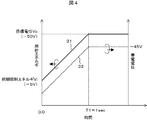
- FIG. 4 shows a time chart 31 when continuously changing the irradiation energy.
- FIG. 4 also shows changes in the charging potential 32 of the sample.
- the target potential Vc is set to -50V
- charges are accumulated while maintaining the incident energy of 5 eV, and the sample can be charged to -45V.
- FIG. 5 shows a time chart when the irradiation energy is changed in steps.
- the initial irradiation energy and the voltage pitch Vp of change need to be in the range of El to Eh shown in FIG.
- the sample is irradiated with energy in the range from El to Eh, so that the charging process can be performed with high charge accumulation efficiency.
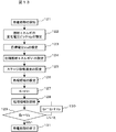
- FIG. 6 shows the flowchart.
- the sample 10 is transferred to the apparatus by the sample transfer unit 11 and evacuated, and then introduced into the observation chamber (step 101).
- the sample 10 is transferred to the sample charging processing system by the XYZ stage 8 (step 102).
- the characteristics of the charge storage efficiency with respect to the incident energy are acquired as shown in FIG. 3 (step 103).
- an incident energy region in which the charge accumulation efficiency is 1 is used.
- the charge accumulation efficiency is not limited to 1, and it is desirable that the charge accumulation efficiency is 0.8 or more in view of the required accuracy of the charging process.
- the incident energy to be used is set, and the initial irradiation energy Vi of the electron source 28 is set (step 104).
- the target potential Vc for the charging process is set (step 105), a signal for changing the irradiation energy is transmitted from the waveform generation unit 24 to the electron source control unit 23, and the irradiation energy of the electron source 28 is changed toward the target potential Vc. (Step 106).
- the charge storage efficiency during electron beam irradiation is measured while monitoring the leakage current, and the rate of change in irradiation energy while monitoring that the charge storage efficiency is 1 by the calculation unit mounted on the waveform generation unit 24 Is adjusted (step 107).
- the charge accumulation efficiency is not limited to 1, and it is desirable to monitor with a charge accumulation efficiency of 0.8 or more in view of the required accuracy of the charging process.
- a method of changing the irradiation energy of the electron source 28 is used, but there are a method of controlling the voltage applied to the sample and a method of controlling the irradiation angle as other methods.
- the voltage pitch of the change in irradiation energy needs to change the irradiation energy at a pitch included in the incident energy band from El to Eh. When El is 0 eV, as shown in FIG. The change in energy can be continuous.
- the conditions of the electron optical system are set as the sample observation conditions (step 108).
- the charged potential of the sample is fed back to the electron gun control unit 13 and the irradiation energy during observation is adjusted.
- the sample is observed using the potential contrast (step 109). After the observation, the sample is taken out from the electron microscope by the sample transport system 11 (step 110).
- the procedure of measuring the incident energy with high charge storage efficiency for each sample as in steps 103 and 104 is adopted.
- the incident energy is made into a database for each material, film thickness, and manufacturing method of the sample, and is observed for each observation. It is also possible to call up from the database stored in the data storage unit 27 through the control computer 25 and set the incident energy.
- the above-described steps 103 and 104 can be omitted by setting the initial irradiation energy to 0 V.
- the initial charging of the sample is important. It is desirable to measure the initial potential of the sample surface in advance or to remove the charge from the sample.
- a method of changing the irradiation energy from the irradiation energy region where the electron beam is bounced is also effective.
- FIG. 7 shows the result of comparing the target potential with the charged potential formed by charging the resist film using the flowchart.
- the measurement result 33 is the result of the charging process using this example. It can be seen that the sample charge according to the target potential Vc can be formed and the charge process can be performed with good control.
- the measurement result 34 is a result of setting the irradiation energy to the target potential Vc from the beginning, which is the conventional charging process method, and performing the charging process, while the measurement result 33 can be controlled from 0 V to ⁇ 50 V. As a result, charge 34 can be formed only up to -20V. As described above, by using the present embodiment, it is possible to accumulate charges with high density in a controlled manner, and it is possible to observe a high quality sample.
- FIG. 8 shows a sample charging system that realizes this embodiment.
- the sample charging system includes an electron source 28 that processes sample charging, an ellipsometer 35 that can measure the dielectric constant and thickness of the sample, a knife-edge ammeter 36 that can measure the irradiation current and irradiation area of the electron beam for charging treatment, It is composed of a surface electrometer 37.
- the rate of change in irradiation energy is defined as the change gradient ⁇ of irradiation energy (target potential / time required for change).
- the change gradient ⁇ of the irradiation energy needs to be set to be equal to or less than the inclination threshold value of the equation (2).
- Tilt threshold irradiation current / sample volume (2)
- Sample capacity sample dielectric constant ⁇ irradiated area / sample thickness (3)
- FIG. 9 shows the relationship 38 between the irradiation energy change gradient ⁇ and the sample charging potential when the target potential is set to ⁇ 50 V and the irradiation energy is changed from 0 V to the target potential.
- the sample charge was measured with a surface potential meter 37.
- the charging potential was normalized with the target potential Vc.
- the position of the inclination threshold 39 according to the equations (2) and (3) is shown.
- the charging potential / target potential is high-efficiency charging process of 0.8 or more, while the change inclination ⁇ is the inclination threshold 39 or more, Only half the target potential can be charged.
- the change slope ⁇ is equal to or greater than the slope threshold value 39, the amount of charge applied to the sample is insufficient, and the sample charging potential cannot be increased. Therefore, the incident energy is increased due to the change in the irradiation energy, so that the charge accumulation efficiency is deteriorated and high-density charge accumulation cannot be performed.
- the change slope ⁇ is equal to or less than the slope threshold 39, there is a sufficient amount of irradiation charge, and the incident energy is maintained in the incident energy band having a high charge storage efficiency, so that high-density charge storage is possible.
- FIG. 10 is a flowchart showing a method for setting the tilt threshold in the present embodiment.
- the ellipsometer 33 measures the dielectric constant and sample thickness of the sample in order to determine the sample capacity (step 111). Further, the irradiation area and the irradiation current are measured by the knife edge type ammeter 34 (step 112).
- the inclination threshold 39 is calculated from the equations (2) and (3) (step 113). An inclination ⁇ of change that is equal to or less than the inclination threshold 39 is set (step 114), a target potential Vc for charging is set (step 115), and an initial irradiation energy Vi is set (step 116).
- the initial irradiation energy was set to 0 V because the incident energy band in which the charge of SiO2 does not flow out is from 0 eV to 5 eV.
- Step 106 of FIG. 6 is performed, and charging processing and observation are performed according to the flowchart of FIG.
- any value can be set as the change inclination ⁇ as long as it is equal to or less than the inclination threshold 39.
- the inclination threshold 39 When set to a value equivalent to the inclination threshold 39, the inclination threshold 39 changes with time variation of the irradiation current, so it is set to the inclination of the change in irradiation energy considering the irradiation current fluctuation or during the charging process It is desirable to use a method of measuring the irradiation current change and controlling the inclination ⁇ of the irradiation energy change in accordance with the change of the inclination threshold 39.
- the inclination threshold value 39 set by the flowchart of the present embodiment can be stored in the data storage unit 27 as a database, and can be called up and used each time.
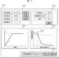
- FIG. 11 shows a GUI that facilitates the condition setting of this embodiment.
- a charging process execution GUI 201 is displayed on the control computer 23.
- the steps 111 and 112 can be acquired and the inclination threshold 39 can be calculated.
- a charging process sequence can be set as in steps 114, 115, and 116.
- the charging processing sequence set at this time is displayed in the window 204.
- the effect can be confirmed as shown in FIG.
- a broken line 206 in the window 205 is the inclination threshold 39.
- the charging process is performed over the electron beam irradiation region by scanning the sample with an electron source for charging processing.
- scanning is controlled by moving the XYZ stage 8 to which the sample holder is attached. Scanning can also be controlled by the movement of the charging electron source.
- the time required for one change in irradiation energy must be less than the speed at which the irradiation region moves. That is, the stage speed threshold value Vlim is determined by equation (4).
- Vlim Irradiation area of the electron source for charging treatment / Time Tr required for one irradiation energy change (4) Further, the time Tr required for one irradiation energy change is determined by equation (5).
- FIG. 12 is a flowchart showing the charging method in this embodiment.
- the setting of the inclination ⁇ of the irradiation energy change (step 114), the setting of the target potential Vc (step 115), and the setting of the initial irradiation energy Vi are performed (step 116).
- the stage movement speed threshold Vlim is calculated from the equations (4) and (5) (step 117). The stage speed is determined so as to be equal to or less than the calculated speed threshold value Vlim (step 118).
- the present embodiment can be executed at any speed as long as it is equal to or less than the speed threshold Vlim, but it is desirable to set the stage speed equal to the speed threshold Vlim in view of the charging processing speed.
- the irradiation energy is changed according to the set parameters (step 119), and a desired charging process area is scanned at the set stage speed (step 120).
- step 108 and subsequent steps shown in FIG. 6 are performed to observe the sample. According to the present embodiment, it is possible to realize high-density charge accumulation of a sample having a large charge processing area.
- the present embodiment by taking into consideration the gradient ⁇ of the change in irradiation energy and the stage speed, it is possible to accumulate a high-density charge in a sample having a large charge processing region.
- This example describes another method and apparatus for processing a sample with a large charged area.
- the irradiation energy at the time of charge control is changed in steps based on the voltage pitch.
- the stage is moved for each irradiation energy step.
- the apparatus configuration is the same as that shown in FIG. With this method, it is not necessary to change the irradiation energy while forming the irradiation region, so that the processing can be performed without depending on the control speed of the charging processing control unit 22.
- the charging process is performed (step 121).
- the change voltage pitch Vp of the irradiation energy when changing the irradiation energy in steps is set (step 122).
- the voltage pitch Vp of the change of irradiation energy is a range included in the incident energy band from El to Eh shown in FIG.
- the target potential Vc and the initial irradiation energy Vi are set (steps 123 and 124).
- the moving speed of the stage is desirably a speed at which a sufficient charge can be irradiated with respect to the voltage charged by one-step irradiation (step 125). Further, after setting the processing area (step 126), the charging process is executed.
- the charging process is performed with the initial irradiation energy Vi and the charging process for the entire processing region is first performed at a set stage speed (steps 127 and 128). If the irradiation energy Er has not reached the target voltage Vc after the entire region has been processed, the irradiation energy is increased at the voltage pitch Vp (steps 129 and 130). Again, the entire processing region is charged, and this processing is repeated up to the target potential Vc. If the irradiation energy Er increases to the target potential Vc, the charging process is finished (step 131).
- charging processing independent of the performance of the charging processing control unit 22 is possible, and high-density charges can be easily stored.
- the apparatus configuration is the same as that shown in FIG. 1, but an electron source whose irradiation energy varies within the irradiation surface is used as the charged electron source of the charging processing unit.
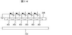
- An example of an electron source whose irradiation energy changes within the irradiation surface is shown in FIG.
- the electron source 28 for charging is composed of an electron source 40 capable of controlling irradiation energy. Since the initial irradiation energy is often -5V and the target potential Vc is often within -50V, it is desirable that the electron source 40 is composed of about ten. In that case, incident energy of ⁇ 5 V, ⁇ 10 V, ⁇ 15 V,... ⁇ 45 V, ⁇ 50 V is applied to the divided electron source 40 in order from the left side.
- the sample can be charged by moving the electron source 40 relative to the sample 10 in the left direction while maintaining the incident energy with high charge storage efficiency.
- the electron source 40 in FIG. 12 is configured by a resistor instead of a power source, and the distribution of irradiation energy can be controlled by supplying a current.
- the distribution of irradiation energy can be controlled in the same manner as described above by using a resistor in the irradiation energy application unit. If the electron source for the charging process of this embodiment is used, a process for changing the irradiation energy is not required, and the charging process speed is not limited by the change gradient ⁇ , so that a high-speed process can be performed.
- Electron microscope 2 Electron gun 3 Condenser lens 4 Alignment coil 5 Deflector 6 Objective lens 7 Detector 8 XYZ stage 9 Sample holder 10
- Sample 11 Sample transport unit 12 Vacuum exhaust system 13
- Electron gun control unit 14 Condenser lens control unit 15 Alignment coil Control unit 16 Deflection control unit 17
- Objective lens control unit 18
- Detection signal processing unit 20
- Stage control unit 21 Vacuum pumping control unit 22
- Charging process control unit 23 Charging process control unit 23
- Electron source control unit 24 Waveform generation unit 25 Control computer 26 Display unit 27 Data storage unit 28
- Electron source for charging 29 29
- Faraday cup 32
- Irradiation energy time chart 32
- Sample charging potential 33
- Charging potential formed by the present invention 34
- Charging potential formed by conventional method 35
- Surface electrometer 38
- Charging potential when tilt changes 39
Landscapes
- Chemical & Material Sciences (AREA)
- Analytical Chemistry (AREA)
- Analysing Materials By The Use Of Radiation (AREA)
Abstract
Description
照射電流は、試料帯電を処理する電子源28から試料位置に到達する電子線の電流で、ファラデーカップ30に電子線を照射し、試料ホルダを介して電流計29で計測できる。リーク電流は電子線を試料10に照射した際に試料から流出する電荷の流れで、試料帯電を処理する電子源28からの電子線を試料10に照射し、試料ホルダを介して電流計29で計測できる。
試料容量は(3)式により求められる
試料容量=試料誘電率×照射領域/試料厚さ (3)
本実施例ではSi基板上に成膜したSiO2試料を例に照射エネルギの変化の傾きαの効果について説明する。図9には目標電位を-50Vに設定し、0Vから目標電位まで照射エネルギを変化させたときの、照射エネルギの変化傾きαと試料帯電電位の関係38について示した。試料帯電は表面電位計37で測定した。帯電電位は目標電位Vcで規格化した。また図中には(2)(3)式による傾き閾値39の位置を示した。傾き閾値39以下の変化の傾きαで帯電処理した場合、帯電電位/目標電位は0.8以上の高効率な帯電処理ができているのに対し、変化の傾きαが傾き閾値39以上である場合、目標電位半分以下しか帯電できていない。変化傾きαが傾き閾値39以上である場合、試料への照射電荷量が不十分なため、試料帯電電位が上昇できない。よって、照射エネルギの変化によって入射エネルギが高まるため、電荷蓄積効率が悪化し、高密度な電荷蓄積ができない。傾き閾値39以下の変化傾きαであれば、十分な照射電荷量があり、入射エネルギが電荷蓄積効率の高い入射エネルギ帯内に維持されるため、高密度な電荷蓄積が可能となる。
また、1回の照射エネルギ変化にかかる時間Trは(5)式で決定される。
本実施例における帯電処理方法を示したフローチャートを図12に示す。前記実施例図10のフローチャートに従い、照射エネルギの変化の傾きαの設定(ステップ114)、目標電位Vcの設定(ステップ115)、初期照射エネルギViの設定を実施する(ステップ116)。次に前記(4)(5)式からステージ移動の速度閾値Vlimを算出する(ステップ117)。算出された速度閾値Vlim以下となるようステージ速度を決定する(ステップ118)。このとき速度閾値Vlim以下であれば、どの速度においても、本実施例を実行することが可能であるが、帯電処理の速度に鑑み、速度閾値Vlimと同等のステージ速度に設定することが望ましい。その後設定したパラメータにより照射エネルギを変化させ(ステップ119)、設定したステージ速度で所望の帯電処理領域を走査する(ステップ120)。帯電処理終了後、前記図6記載のステップ108以降を実施し、試料の観察を行う。本実施例により、帯電処理領域が大きい試料の高密度な電荷蓄積を実現することができる。
2 電子銃
3 コンデンサレンズ
4 アライメントコイル
5 偏向器
6 対物レンズ
7 検出器
8 XYZステージ
9 試料ホルダ
10 試料
11 試料搬送部
12 真空排気系
13 電子銃制御部
14 コンデンサレンズ制御部
15 アライメントコイル制御部
16偏向制御部
17 対物レンズ制御部
18 検出器制御部
19 検出信号処理部
20 ステージ制御部
21 真空排気制御部
22 帯電処理制御部
23 電子源制御部
24 波形生成部
25 制御コンピュータ
26 表示部
27 データ記憶部
28 帯電処理用電子源
29 電流計
30 ファラデーカップ
31 照射エネルギのタイムチャート
32 試料帯電電位
33 本発明によって形成した帯電電位
34 従来の方法で形成した帯電電位
35 エリプソメータ
36 ナイフエッジ式照射電流計
37 表面電位計
38 傾き変化時の帯電電位
39 傾き閾値
40 電子源
201 帯電処理実施GUI
202,203,204,205,207 ウィンドウ
206 傾き閾値
Claims (15)
- 電子線を試料に入射して前記試料から放出される電子を検出する電子線を用いた試料観察方法において、
低入射エネルギ領域で電荷蓄積効率が高い第一の入射エネルギ帯を持つ電子線を前記試料に照射して試料を帯電させる工程と、
前記試料を帯電させる工程の後に、第二の入射エネルギを持つ電子線を前記試料に照射して電位コントラストを利用した試料の観察を実施する工程と、
を有することを特徴とする電子線を用いた試料観察方法。 - 電子線を試料に入射して前記試料から放出される電子を検出する電子線を用いた試料観察方法において、
電子線照射時の電荷蓄積効率が高い入射エネルギ帯に含まれる第一の入射エネルギを持つ電子線を前記試料に照射する工程と、
前記第一の入射エネルギを維持したまま、前記電子線の照射エネルギを帯電処理の目標電位まで変化させて試料を帯電させる工程と、
前記試料を帯電させる工程の後に第二の入射エネルギを持つ電子線を前記試料に照射して電位コントラストを利用した試料の観察を実施する工程と、
を有することを特徴とする電子線を用いた試料観察方法。 - 電子線を試料に入射して前記試料から放出される電子を検出する電子線を用いた試料観察方法において、
電子線照射時の電荷蓄積効率が高い入射エネルギ帯に含まれる第一の入射エネルギを持つ電子線を前記試料に照射する工程と、
前記電子線照射中に前記試料から流れる電流を監視しながら、前記電子線の照射エネルギを帯電処理の目標電位まで変化させて試料を帯電させる工程と、
前記試料を帯電させる工程の後に第二の入射エネルギを持つ電子線を前記試料に照射して電位コントラストを利用した試料の観察を実施する工程と、
を有することを特徴とする電子線を用いた試料観察方法。 - 請求項2または請求項3記載の電子線を用いた試料観察方法であって、
前記照射エネルギを変化させる速度を、試料の静電容量と照射電流から決まる閾値以下に設定することを特徴とする電子線を用いた試料観察方法。 - 請求項2または請求項3記載の電子線を用いた試料観察方法であって、
さらに、前記電子線で前記試料を走査して帯電処理領域が大きい試料を帯電させる工程を含み、照射エネルギを変化させる速度に応じて、電子線で試料を走査する速度を設定することを特徴とする電子線を用いた試料観察方法。 - 電子線を試料に入射して前記試料から放出される電子を検出する電子線を用いた試料観察方法において、
電子線照射時の電荷蓄積効率が高い入射エネルギ帯に含まれる第一の入射エネルギを持つ電子線を前記試料に照射する工程と、
前記第一の入射エネルギを持つ電子線で、前記試料を走査する工程と、
前記第一の入射エネルギを維持する電圧ピッチで、前記電子線の照射エネルギを変化させる工程と、
前記変化された電子線の照射エネルギで、再度、電子線を前記試料に照射する工程と、
第一の入射エネルギを持つ電子線で、再度、前記試料を走査する工程と、
前記電子線の照射エネルギを変化させる工程、電子線を前記試料に照射する工程、および前記試料を走査する工程を繰り返すことにより、帯電処理の目標電位まで帯電処理領域が大きい試料を帯電させる工程と、
前記試料を帯電させる工程の後に第二の入射エネルギを持つ電子線を前記試料に照射して電位コントラストを利用した試料の観察を実施する工程と、
を有することを特徴とする電子線を用いた試料観察方法。 - 請求項1、請求項2、請求項3、請求項6のいずれか一つに記載の電子線を用いた試料観察方法であって、
第一の入射エネルギ帯もしくは第一の入射エネルギが0から10eVまでであることを特徴とする電子線を用いた試料観察方法。 - 請求項1、請求項2、請求項3、請求項6のいずれか一つに記載の電子線を用いた試料観察方法であって、
前記電荷蓄積効率が0.8以上であることを特徴とする電子線を用いた試料観察方法。 - 電子線を放出する電子銃と、
前記電子線を試料に照射する電子光学系と、
前記試料を保持する試料ホルダと、
前記試料から放出される電子を検出する検出器と、
照射エネルギ制御が可能な第二の電子源と、
照射エネルギの変化波形を生成する波形生成装置と、
前記照射エネルギの変化波形に基づき、電子線照射時の電荷蓄積効率が高い入射エネルギ帯に含まれる入射エネルギを維持したまま、前記第二の電子源の電子線の照射エネルギを変化させる照射エネルギ制御装置と、
を有することを特徴とする電子顕微鏡。 - 照射エネルギを制御された電子線を放出する電子銃と、
前記電子線を試料に照射する電子光学系と、
前記試料を保持する試料ホルダと、
前記試料から放出される電子を検出する検出器と、
前記電子線の電荷の蓄積効率を測定する電荷蓄積効率測定装置と、
照射エネルギの変化波形を生成する波形生成装置と、
前記照射エネルギの変化波形に基づき、前記電荷の蓄積効率の測定結果に応じて、電子線照射時の電荷蓄積効率が高い入射エネルギ帯に含まれる入射エネルギを維持したまま、前記電子線の照射エネルギを変化させる照射エネルギ制御装置と、
を有することを特徴とする電子顕微鏡。 - 電子線を放出する電子銃と、
前記電子線を試料に照射する電子光学系と、
前記試料を保持する試料ホルダと、
前記試料から放出される電子を検出する検出器と、
照射エネルギ制御が可能な第二の電子源と、
前記第二の電子源からの電子線の電荷の蓄積効率を測定する電荷蓄積効率測定装置と、
照射エネルギの変化波形を生成する波形生成装置と、
前記照射エネルギの変化波形に基づき、前記電荷の蓄積効率の測定結果に応じて、電子線照射時の電荷蓄積効率が高い入射エネルギ帯に含まれる入射エネルギを維持したまま、前記第二の電子源からの電子線の照射エネルギを変化させる照射エネルギ制御装置と、
を有することを特徴とする電子顕微鏡。 - 請求項9乃至請求項11のいずれか一つに記載の電子顕微鏡において、
前記照射エネルギ制御装置が、電子線の前記電子源に印加する電圧と前記試料に印加する電圧とを制御するものであることを特徴とする電子顕微鏡。 - 請求項9乃至請求項11のいずれか一つに記載の電子顕微鏡において、
さらに、試料ホルダを移動させる移動機構を備え、該移動機構は、照射エネルギ制御装置の変化波形に基づき試料ホルダを移動させる速度を設定する速度制御装置と、設定された速度に基づき試料ホルダを移動させるステージ装置を備えることを特徴とする電子顕微鏡 - 請求項10または請求項11に記載の電子顕微鏡において、
前記電荷蓄積効率測定装置が、照射電流を測定する照射電流計と電子線照射時の帯電電位を測定する表面電位計を備えることを特徴とする電子顕微鏡。 - 電子線を放出する電子銃と、
前記電子線を試料に照射する電子光学系と、
前記試料を保持する試料ホルダと、
前記試料から放出される電子を検出する検出器と、
初期照射エネルギから目標電圧までの段階的な照射エネルギが順次印加される複数に分割された電子源と、
電子線照射時の電荷蓄積効率が高い入射エネルギ帯に含まれる入射エネルギを維持するような速度で、前記試料ホルダと前記電子源とを相対的に移動させる移動機構と、
を有することを特徴とする電子顕微鏡。
Priority Applications (2)
| Application Number | Priority Date | Filing Date | Title |
|---|---|---|---|
| US13/508,774 US20120292506A1 (en) | 2009-11-13 | 2010-11-08 | Sample observation method using electron beams and electron microscope |
| JP2011540499A JP5406308B2 (ja) | 2009-11-13 | 2010-11-08 | 電子線を用いた試料観察方法及び電子顕微鏡 |
Applications Claiming Priority (2)
| Application Number | Priority Date | Filing Date | Title |
|---|---|---|---|
| JP2009-259980 | 2009-11-13 | ||
| JP2009259980 | 2009-11-13 |
Publications (1)
| Publication Number | Publication Date |
|---|---|
| WO2011058950A1 true WO2011058950A1 (ja) | 2011-05-19 |
Family
ID=43991609
Family Applications (1)
| Application Number | Title | Priority Date | Filing Date |
|---|---|---|---|
| PCT/JP2010/069845 Ceased WO2011058950A1 (ja) | 2009-11-13 | 2010-11-08 | 電子線を用いた試料観察方法及び電子顕微鏡 |
Country Status (3)
| Country | Link |
|---|---|
| US (1) | US20120292506A1 (ja) |
| JP (1) | JP5406308B2 (ja) |
| WO (1) | WO2011058950A1 (ja) |
Cited By (2)
| Publication number | Priority date | Publication date | Assignee | Title |
|---|---|---|---|---|
| KR20160014560A (ko) * | 2014-07-29 | 2016-02-11 | 어플라이드 머티리얼즈 이스라엘 리미티드 | 하전 입자 빔 시료 검사 시스템 및 그 동작 방법 |
| WO2022208572A1 (ja) * | 2021-03-29 | 2022-10-06 | 株式会社日立ハイテク | 検査システム |
Families Citing this family (4)
| Publication number | Priority date | Publication date | Assignee | Title |
|---|---|---|---|---|
| US9805910B1 (en) * | 2015-03-14 | 2017-10-31 | Kla-Tencor Corporation | Automated SEM nanoprobe tool |
| CN111433881B (zh) | 2017-09-29 | 2023-09-15 | Asml荷兰有限公司 | 样品检查中的图像对比度增强 |
| JP2020017415A (ja) * | 2018-07-26 | 2020-01-30 | 株式会社日立ハイテクノロジーズ | 荷電粒子線装置 |
| DE102023205886A1 (de) * | 2023-06-22 | 2024-12-24 | Carl Zeiss Smt Gmbh | Verhindern von ESD in PRT SEM Entladungen |
Citations (4)
| Publication number | Priority date | Publication date | Assignee | Title |
|---|---|---|---|---|
| JP2004014485A (ja) * | 2002-06-12 | 2004-01-15 | Hitachi High-Technologies Corp | ウェハ欠陥検査方法及びウェハ欠陥検査装置 |
| JP2005333161A (ja) * | 2005-08-05 | 2005-12-02 | Renesas Technology Corp | 荷電粒子ビームを用いた検査装置 |
| JP2006234789A (ja) * | 2005-01-26 | 2006-09-07 | Hitachi High-Technologies Corp | 帯電制御装置及び帯電制御装置を備えた計測装置 |
| JP2007265931A (ja) * | 2006-03-30 | 2007-10-11 | Hitachi High-Technologies Corp | 検査装置及び検査方法 |
Family Cites Families (3)
| Publication number | Priority date | Publication date | Assignee | Title |
|---|---|---|---|---|
| US6504393B1 (en) * | 1997-07-15 | 2003-01-07 | Applied Materials, Inc. | Methods and apparatus for testing semiconductor and integrated circuit structures |
| WO2000072355A1 (en) * | 1999-05-25 | 2000-11-30 | Kla-Tencor Corporation | Apparatus and methods for secondary electron emission microscopy with dual beam |
| US6627884B2 (en) * | 2001-03-19 | 2003-09-30 | Kla-Tencor Technologies Corporation | Simultaneous flooding and inspection for charge control in an electron beam inspection machine |
-
2010
- 2010-11-08 US US13/508,774 patent/US20120292506A1/en not_active Abandoned
- 2010-11-08 JP JP2011540499A patent/JP5406308B2/ja not_active Expired - Fee Related
- 2010-11-08 WO PCT/JP2010/069845 patent/WO2011058950A1/ja not_active Ceased
Patent Citations (4)
| Publication number | Priority date | Publication date | Assignee | Title |
|---|---|---|---|---|
| JP2004014485A (ja) * | 2002-06-12 | 2004-01-15 | Hitachi High-Technologies Corp | ウェハ欠陥検査方法及びウェハ欠陥検査装置 |
| JP2006234789A (ja) * | 2005-01-26 | 2006-09-07 | Hitachi High-Technologies Corp | 帯電制御装置及び帯電制御装置を備えた計測装置 |
| JP2005333161A (ja) * | 2005-08-05 | 2005-12-02 | Renesas Technology Corp | 荷電粒子ビームを用いた検査装置 |
| JP2007265931A (ja) * | 2006-03-30 | 2007-10-11 | Hitachi High-Technologies Corp | 検査装置及び検査方法 |
Cited By (7)
| Publication number | Priority date | Publication date | Assignee | Title |
|---|---|---|---|---|
| KR20160014560A (ko) * | 2014-07-29 | 2016-02-11 | 어플라이드 머티리얼즈 이스라엘 리미티드 | 하전 입자 빔 시료 검사 시스템 및 그 동작 방법 |
| JP2016031937A (ja) * | 2014-07-29 | 2016-03-07 | アプライド マテリアルズ イスラエル リミテッド | 荷電粒子ビーム試料検査システムおよびその動作方法 |
| US10522327B2 (en) | 2014-07-29 | 2019-12-31 | Applied Materials Israel Ltd. | Method of operating a charged particle beam specimen inspection system |
| KR102373865B1 (ko) | 2014-07-29 | 2022-03-14 | 어플라이드 머티리얼즈 이스라엘 리미티드 | 하전 입자 빔 시료 검사 시스템 및 그 동작 방법 |
| WO2022208572A1 (ja) * | 2021-03-29 | 2022-10-06 | 株式会社日立ハイテク | 検査システム |
| JPWO2022208572A1 (ja) * | 2021-03-29 | 2022-10-06 | ||
| JP7481574B2 (ja) | 2021-03-29 | 2024-05-10 | 株式会社日立ハイテク | 検査システム |
Also Published As
| Publication number | Publication date |
|---|---|
| US20120292506A1 (en) | 2012-11-22 |
| JP5406308B2 (ja) | 2014-02-05 |
| JPWO2011058950A1 (ja) | 2013-04-04 |
Similar Documents
| Publication | Publication Date | Title |
|---|---|---|
| TWI631343B (zh) | 檢測帶電荷試件表面的方法及裝置 | |
| JP5937171B2 (ja) | 走査型電子顕微鏡及び試料観察方法 | |
| US7989768B2 (en) | Scanning electron microscope | |
| US9202665B2 (en) | Charged particle beam apparatus for removing charges developed on a region of a sample | |
| TWI787631B (zh) | 帶電粒子束裝置 | |
| JP5406308B2 (ja) | 電子線を用いた試料観察方法及び電子顕微鏡 | |
| JP2003202217A (ja) | パターン欠陥検査方法及びパターン欠陥検査装置 | |
| EP2426559A2 (en) | Device and method for measuring surface charge distribution | |
| US6734429B2 (en) | Electron microscope charge-up prevention method and electron microscope | |
| JP7149906B2 (ja) | 走査電子顕微鏡及びパタン計測方法 | |
| US9202668B2 (en) | Observation specimen for use in electron microscopy, electron microscopy, electron microscope, and device for producing observation specimen | |
| JP4089580B2 (ja) | 薄膜の厚さ及び厚さ分布の評価方法 | |
| JP5074262B2 (ja) | 帯電電位測定方法、及び荷電粒子顕微鏡 | |
| US8507857B2 (en) | Charged particle beam inspection apparatus and inspection method using charged particle beam | |
| JP4238072B2 (ja) | 荷電粒子線装置 | |
| WO2022185390A1 (ja) | 荷電粒子線装置 | |
| JP5016799B2 (ja) | 荷電粒子ビームを用いた検査装置 | |
| US7205539B1 (en) | Sample charging control in charged-particle systems | |
| JP5548244B2 (ja) | 検査計測装置および検査計測方法 | |
| JP4906409B2 (ja) | 電子ビーム寸法測定装置及び電子ビーム寸法測定方法 | |
| JP6230831B2 (ja) | 荷電粒子線装置および画像取得方法 | |
| JP5188263B2 (ja) | 走査電子顕微鏡 | |
| Ohta et al. | Development of micro focus X-ray microscope equipped with high brightness Li/W< 111> field emitter | |
| JP2010118192A (ja) | 電子ビームを用いた装置 |
Legal Events
| Date | Code | Title | Description |
|---|---|---|---|
| 121 | Ep: the epo has been informed by wipo that ep was designated in this application |
Ref document number: 10829909 Country of ref document: EP Kind code of ref document: A1 |
|
| WWE | Wipo information: entry into national phase |
Ref document number: 2011540499 Country of ref document: JP |
|
| WWE | Wipo information: entry into national phase |
Ref document number: 13508774 Country of ref document: US |
|
| NENP | Non-entry into the national phase |
Ref country code: DE |
|
| 122 | Ep: pct application non-entry in european phase |
Ref document number: 10829909 Country of ref document: EP Kind code of ref document: A1 |