WO2011058720A1 - Semiconductor device - Google Patents
Semiconductor device Download PDFInfo
- Publication number
- WO2011058720A1 WO2011058720A1 PCT/JP2010/006475 JP2010006475W WO2011058720A1 WO 2011058720 A1 WO2011058720 A1 WO 2011058720A1 JP 2010006475 W JP2010006475 W JP 2010006475W WO 2011058720 A1 WO2011058720 A1 WO 2011058720A1
- Authority
- WO
- WIPO (PCT)
- Prior art keywords
- integrated circuit
- semiconductor integrated
- disposed
- pad
- electric
- Prior art date
- Legal status (The legal status is an assumption and is not a legal conclusion. Google has not performed a legal analysis and makes no representation as to the accuracy of the status listed.)
- Ceased
Links
Images


Classifications
-
- H—ELECTRICITY
- H10—SEMICONDUCTOR DEVICES; ELECTRIC SOLID-STATE DEVICES NOT OTHERWISE PROVIDED FOR
- H10W—GENERIC PACKAGES, INTERCONNECTIONS, CONNECTORS OR OTHER CONSTRUCTIONAL DETAILS OF DEVICES COVERED BY CLASS H10
- H10W44/00—Electrical arrangements for controlling or matching impedance
-
- H—ELECTRICITY
- H10—SEMICONDUCTOR DEVICES; ELECTRIC SOLID-STATE DEVICES NOT OTHERWISE PROVIDED FOR
- H10W—GENERIC PACKAGES, INTERCONNECTIONS, CONNECTORS OR OTHER CONSTRUCTIONAL DETAILS OF DEVICES COVERED BY CLASS H10
- H10W42/00—Arrangements for protection of devices
- H10W42/20—Arrangements for protection of devices protecting against electromagnetic or particle radiation, e.g. light, X-rays, gamma-rays or electrons
- H10W42/261—Arrangements for protection of devices protecting against electromagnetic or particle radiation, e.g. light, X-rays, gamma-rays or electrons characterised by their shapes or dispositions
- H10W42/265—Shielding wires, e.g. constant potential wires
-
- H—ELECTRICITY
- H10—SEMICONDUCTOR DEVICES; ELECTRIC SOLID-STATE DEVICES NOT OTHERWISE PROVIDED FOR
- H10W—GENERIC PACKAGES, INTERCONNECTIONS, CONNECTORS OR OTHER CONSTRUCTIONAL DETAILS OF DEVICES COVERED BY CLASS H10
- H10W72/00—Interconnections or connectors in packages
-
- H—ELECTRICITY
- H10—SEMICONDUCTOR DEVICES; ELECTRIC SOLID-STATE DEVICES NOT OTHERWISE PROVIDED FOR
- H10W—GENERIC PACKAGES, INTERCONNECTIONS, CONNECTORS OR OTHER CONSTRUCTIONAL DETAILS OF DEVICES COVERED BY CLASS H10
- H10W42/00—Arrangements for protection of devices
- H10W42/20—Arrangements for protection of devices protecting against electromagnetic or particle radiation, e.g. light, X-rays, gamma-rays or electrons
-
- H—ELECTRICITY
- H10—SEMICONDUCTOR DEVICES; ELECTRIC SOLID-STATE DEVICES NOT OTHERWISE PROVIDED FOR
- H10W—GENERIC PACKAGES, INTERCONNECTIONS, CONNECTORS OR OTHER CONSTRUCTIONAL DETAILS OF DEVICES COVERED BY CLASS H10
- H10W44/00—Electrical arrangements for controlling or matching impedance
- H10W44/20—Electrical arrangements for controlling or matching impedance at high-frequency [HF] or radio frequency [RF]
- H10W44/203—Electrical connections
- H10W44/206—Wires
-
- H—ELECTRICITY
- H10—SEMICONDUCTOR DEVICES; ELECTRIC SOLID-STATE DEVICES NOT OTHERWISE PROVIDED FOR
- H10W—GENERIC PACKAGES, INTERCONNECTIONS, CONNECTORS OR OTHER CONSTRUCTIONAL DETAILS OF DEVICES COVERED BY CLASS H10
- H10W72/00—Interconnections or connectors in packages
- H10W72/071—Connecting or disconnecting
- H10W72/075—Connecting or disconnecting of bond wires
-
- H—ELECTRICITY
- H10—SEMICONDUCTOR DEVICES; ELECTRIC SOLID-STATE DEVICES NOT OTHERWISE PROVIDED FOR
- H10W—GENERIC PACKAGES, INTERCONNECTIONS, CONNECTORS OR OTHER CONSTRUCTIONAL DETAILS OF DEVICES COVERED BY CLASS H10
- H10W72/00—Interconnections or connectors in packages
- H10W72/071—Connecting or disconnecting
- H10W72/075—Connecting or disconnecting of bond wires
- H10W72/07551—Connecting or disconnecting of bond wires characterised by changes in properties of the bond wires during the connecting
- H10W72/07554—Connecting or disconnecting of bond wires characterised by changes in properties of the bond wires during the connecting changes in dispositions
-
- H—ELECTRICITY
- H10—SEMICONDUCTOR DEVICES; ELECTRIC SOLID-STATE DEVICES NOT OTHERWISE PROVIDED FOR
- H10W—GENERIC PACKAGES, INTERCONNECTIONS, CONNECTORS OR OTHER CONSTRUCTIONAL DETAILS OF DEVICES COVERED BY CLASS H10
- H10W72/00—Interconnections or connectors in packages
- H10W72/50—Bond wires
- H10W72/541—Dispositions of bond wires
- H10W72/5445—Dispositions of bond wires being orthogonal to a side surface of the chip, e.g. parallel arrangements
-
- H—ELECTRICITY
- H10—SEMICONDUCTOR DEVICES; ELECTRIC SOLID-STATE DEVICES NOT OTHERWISE PROVIDED FOR
- H10W—GENERIC PACKAGES, INTERCONNECTIONS, CONNECTORS OR OTHER CONSTRUCTIONAL DETAILS OF DEVICES COVERED BY CLASS H10
- H10W72/00—Interconnections or connectors in packages
- H10W72/50—Bond wires
- H10W72/541—Dispositions of bond wires
- H10W72/5449—Dispositions of bond wires not being orthogonal to a side surface of the chip, e.g. fan-out arrangements
-
- H—ELECTRICITY
- H10—SEMICONDUCTOR DEVICES; ELECTRIC SOLID-STATE DEVICES NOT OTHERWISE PROVIDED FOR
- H10W—GENERIC PACKAGES, INTERCONNECTIONS, CONNECTORS OR OTHER CONSTRUCTIONAL DETAILS OF DEVICES COVERED BY CLASS H10
- H10W72/00—Interconnections or connectors in packages
- H10W72/50—Bond wires
- H10W72/541—Dispositions of bond wires
- H10W72/547—Dispositions of multiple bond wires
-
- H—ELECTRICITY
- H10—SEMICONDUCTOR DEVICES; ELECTRIC SOLID-STATE DEVICES NOT OTHERWISE PROVIDED FOR
- H10W—GENERIC PACKAGES, INTERCONNECTIONS, CONNECTORS OR OTHER CONSTRUCTIONAL DETAILS OF DEVICES COVERED BY CLASS H10
- H10W72/00—Interconnections or connectors in packages
- H10W72/50—Bond wires
- H10W72/541—Dispositions of bond wires
- H10W72/547—Dispositions of multiple bond wires
- H10W72/5473—Dispositions of multiple bond wires multiple bond wires connected to a common bond pad
-
- H—ELECTRICITY
- H10—SEMICONDUCTOR DEVICES; ELECTRIC SOLID-STATE DEVICES NOT OTHERWISE PROVIDED FOR
- H10W—GENERIC PACKAGES, INTERCONNECTIONS, CONNECTORS OR OTHER CONSTRUCTIONAL DETAILS OF DEVICES COVERED BY CLASS H10
- H10W72/00—Interconnections or connectors in packages
- H10W72/50—Bond wires
- H10W72/541—Dispositions of bond wires
- H10W72/547—Dispositions of multiple bond wires
- H10W72/5475—Dispositions of multiple bond wires multiple bond wires connected to common bond pads at both ends of the wires
-
- H—ELECTRICITY
- H10—SEMICONDUCTOR DEVICES; ELECTRIC SOLID-STATE DEVICES NOT OTHERWISE PROVIDED FOR
- H10W—GENERIC PACKAGES, INTERCONNECTIONS, CONNECTORS OR OTHER CONSTRUCTIONAL DETAILS OF DEVICES COVERED BY CLASS H10
- H10W72/00—Interconnections or connectors in packages
- H10W72/50—Bond wires
- H10W72/551—Materials of bond wires
- H10W72/552—Materials of bond wires comprising metals or metalloids, e.g. silver
- H10W72/5522—Materials of bond wires comprising metals or metalloids, e.g. silver comprising gold [Au]
-
- H—ELECTRICITY
- H10—SEMICONDUCTOR DEVICES; ELECTRIC SOLID-STATE DEVICES NOT OTHERWISE PROVIDED FOR
- H10W—GENERIC PACKAGES, INTERCONNECTIONS, CONNECTORS OR OTHER CONSTRUCTIONAL DETAILS OF DEVICES COVERED BY CLASS H10
- H10W72/00—Interconnections or connectors in packages
- H10W72/90—Bond pads, in general
- H10W72/951—Materials of bond pads
-
- H—ELECTRICITY
- H10—SEMICONDUCTOR DEVICES; ELECTRIC SOLID-STATE DEVICES NOT OTHERWISE PROVIDED FOR
- H10W—GENERIC PACKAGES, INTERCONNECTIONS, CONNECTORS OR OTHER CONSTRUCTIONAL DETAILS OF DEVICES COVERED BY CLASS H10
- H10W90/00—Package configurations
- H10W90/701—Package configurations characterised by the relative positions of pads or connectors relative to package parts
- H10W90/751—Package configurations characterised by the relative positions of pads or connectors relative to package parts of bond wires
- H10W90/754—Package configurations characterised by the relative positions of pads or connectors relative to package parts of bond wires between a chip and a stacked insulating package substrate, interposer or RDL
Definitions
- the present invention relates to semiconductor devices on which semiconductor integrated circuits are mounted, and particularly relates to electric-power noise of a semiconductor device.
- a method for implementing a bypass capacitor between a power-supply line and a ground (GND) pattern has been known.
- a capacity of the bypass capacitor is limited, and therefore, it is difficult to sufficiently supply current to a semiconductor device only using current supplied from the bypass capacitor. Therefore, a core power supply unit directly supplies current to the semiconductor device more than a little.
- Japanese Patent Laid-Open No. 2004-140210 discloses a countermeasure against high-frequency noise spreading to a printed circuit board which is generated by supplying current from a core power supply unit.
- Japanese Patent Laid-Open No. 2004-140210 discloses a printed circuit board configured such that a stub wiring is disposed between a bypass capacitor and a core power supply unit so that impedance lower than that of a power-supply path is obtained. That is, current including high-frequency noise is allowed to be supplied to the stub wiring and is reflected at an open end whereby noise current supplied from a semiconductor integrated circuit is cancelled.
- the present invention provides a printed circuit board which achieves high-density implementation and which efficiently suppresses high-frequency noise. Furthermore, the present invention provides a semiconductor device capable of considerably controlling a filter constant in accordance with a semiconductor integrated circuit.
- the present invention provides a semiconductor device including a semiconductor integrated circuit board, a semiconductor integrated circuit implemented on the semiconductor integrated circuit board, pads which are disposed on the semiconductor integrated circuit, and pads which are disposed on the semiconductor integrated circuit board and which are connected to the pads disposed on the semiconductor integrated circuit through bonding wires.
- the bonding wires include an electric-power bonding wire configured to connect an electric-power pad disposed on the semiconductor integrated circuit board to an electric-power pad disposed on the semiconductor integrated circuit, a ground bonding wire configured to connect a ground pad disposed on the semiconductor integrated circuit board to a ground pad disposed on the semiconductor integrated circuit, a signal bonding wire configured to connect a signal pad disposed on the semiconductor integrated circuit board to a signal pad disposed on the semiconductor integrated circuit, and a stub wiring bonding wire configured to connect an electric-power pad disposed on the semiconductor integrated circuit to a non-connected pad which is not electrically connected to any other electric circuit and which is disposed on the semiconductor integrated circuit board.
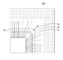
- Fig. 1 is a diagram schematically illustrating a semiconductor device according to a first embodiment.
- Fig. 2 is a diagram schematically illustrating a semiconductor device according to a second embodiment.
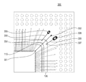
- Fig. 3 is a diagram schematically illustrating a semiconductor device according to a third embodiment.
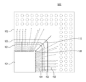
- Fig. 4 is a diagram schematically illustrating a semiconductor device according to another embodiment.
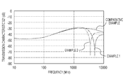
- Fig. 5 is a graph illustrating results of simulations of examples 1 and 2 and a comparative example.
- Fig. 6 is a diagram schematically illustrating a semiconductor device according to the related art.
- a semiconductor device 100 according to a first embodiment of the present invention will be described.
- a semiconductor integrated circuit board 102 is mounted on a semiconductor integrated circuit 101.
- the semiconductor integrated circuit 101 and the semiconductor integrated circuit board 102 are electrically connected to each other through bonding wires 103.
- the bonding wires 103 which supply electric power potentials to the semiconductor integrated circuit 101 are connected to an electric-power potential ring pattern 106 (power-supply pattern) which is disposed on a periphery of the semiconductor integrated circuit 101 disposed on the semiconductor integrated circuit board 102.
- Bonding wires 104 which supply GND potentials to the semiconductor integrated circuit 101 is connected to a GND ring pattern 107 disposed on the semiconductor integrated circuit board 102.
- Bonding wires 105 (signal bonding wires) which allow signals externally input to or output from the semiconductor integrated circuit 101 to be transmitted are connected to a signal pattern, not shown, disposed on the semiconductor integrated circuit board 102.
- the GND ring pattern 107 is disposed on the periphery of the semiconductor integrated circuit 101 and the electric-power potential ring pattern 106 is disposed on the periphery of the GND ring pattern 107.
- the arrangement order of the GND ring pattern 107 and the electric-power potential ring pattern 106 may be reversed.
- an electric-power potential supply pad 108 is disposed on one of the corners of the semiconductor integrated circuit 101.
- the electric-power potential supply pad 108 disposed on the semiconductor integrated circuit 101 is connected to a pad 109 which is not electrically connected to any other electric circuit and which is disposed in a vacant space included in the semiconductor integrated circuit board 102 through a bonding wire 110.
- the pad (stub wiring pad) 109 connected to the bonding wire (stub wiring bonding wire) 110 serving as a stub wiring has a predetermined area. Therefore, a capacitance component is generated between the pad 109 and one of a GND (ground) layer and an electric-power layer which are formed on different layers of the semiconductor integrated circuit board 102. Accordingly, the bonding wire 110 and the pad 109 constitute an LC resonant circuit on the semiconductor integrated circuit 101 in parallel to the GND bonding wires 104.
- the LC resonant circuit can suppress transmission of noise to the semiconductor integrated circuit board 102 since the LC resonant circuit functions as a high-frequency noise filter.
- a length of the bonding wire 110 serving as the stub wiring and a size of the pad 109 are controlled so that the inductance value calculated so as to satisfy Expression (1) corresponds to an integral multiple of a basic operation frequency.
- the bonding wire 110 is disposed in a three-dimensional manner relative to the GND bonding wires 104 and the bonding wires 105. Therefore, the pad 109 may be disposed in any portion in the vacant space of the semiconductor integrated circuit board 102. Accordingly, high degrees of freedom of a pattern length and a pattern width of the bonding wire 110 are attained.
- the vacant space of the semiconductor integrated circuit board 102 is considerably larger than a printed wiring board, and accordingly, implementation of a stub inside the semiconductor device is effective.
- a simulation is performed using the semiconductor device 100 shown in Fig. 1.
- the bonding wire 110 corresponds to a gold line having a diameter of 20 micrometer and a length of 2 mm, and a size of the pad 109 which is not electrically connected to any other electric circuit is formed of a copper foil having a size of 500 micrometer square.
- an inductance value is substantially 2 nH and a capacitance value is substantially 1 pF.
- a characteristic of noise transmission is measured using a pad group which supplies a power supply potential to the bonding wire 110 and a pad group which supplies GND to the bonding wire 110.
- a transmission characteristic (S21) at a time when a signal to be transmitted has a frequency in a range from 10 MHz to 10 GHz is obtained.
- a result of the obtainment is shown in Fig. 5.
- a semiconductor device 200 according to a second embodiment of the present invention will be described. Note that components the same as those shown in Fig. 1 are denoted by reference numerals the same as those shown in Fig. 1.
- a bonding wire 203 is disposed instead of the bonding wire 110 shown in Fig. 1.
- the bonding wire 203 is used to connect an electric-power potentially supply pad 201 disposed on a power-supply potential ring pattern 106 to a pad 202 which is not electrically connected to any other electric circuit and which is disposed on a vacant space of a semiconductor integrated circuit board 102.
- the pad 202 which is connected to the bonding wire 203 serving as a stub wiring has a predetermined area, and a capacitance component is generated between the pad 202 and one of a GND (ground) layer and an electric power layer which are formed in different layers of the semiconductor integrated circuit board 102. Therefore, the bonding wire 203 and the pad 202 constitute an LC resonant circuit in parallel to GND bonding wires 104 which supply electric power potentials to the semiconductor integrated circuit 101. Since the LC resonant circuit functions as a high-frequency noise filter, the LC resonant circuit suppresses transmission of noise to the semiconductor integrated circuit board 102.
- a simulation is performed using the semiconductor device 200 shown in Fig. 2.
- a bonding wire 110 corresponds to a gold line having a diameter of 20 micrometer and a length of 1 mm, and a size of the pad 202 which is not electrically connected to any other electric circuit is formed of a copper foil having a size of 500 micrometer square.
- an inductance value is substantially 1 nH and a capacitance value is substantially 1 pF.
- a characteristic of noise transmission is measured using a pad group which supplies an electric power potential to the bonding wire 110 and a pad group which supplies a reference potential to the bonding wire 110.
- a transmission characteristic (S21) at a time when a signal to be transmitted has a frequency in a range from 10 MHz to 10 GHz is obtained.
- a result of the obtainment is shown in Fig. 5.
- a simulation is performed using a semiconductor device according to the related art shown in Fig. 6.
- a semiconductor device 500 shown in Fig. 6 is different from the semiconductor device 100 shown in Fig. 1 in that the semiconductor device 500 does not include the wire bonding 110 serving as the stub wiring.
- a transmission characteristic (S21) at a time when a signal to be transmitted has a frequency in a range from 10 MHz to 10 GHz is obtained.
- a result of the obtainment is shown in Fig. 5.
- the transmission characteristic (S21) of the example 1 is considerably reduced in a range between 2 GHz to 10 GHz including 5 GHz as a center when compared with the comparative example. Accordingly, noise between the range from 2 GHz to 10 GHz can be considerably suppressed. Furthermore, the transmission characteristic (S21) of the example 2 is considerably reduced in a range from 1 GHz to 8 GHz including 3 GHz as a center when compared with the comparative example. Accordingly, noise between the range from 3 GHz to 8 GHz can be considerably suppressed.
- a bonding wire 306 and a bonding wire 309 are disposed in addition to a bonding wire 110.
- the bonding wire 306 is used to connect an electric-power potential pad 304 disposed on a power-supply potential ring pattern 106 to a pad 305 disposed on a vacant space on the semiconductor integrated circuit board 102.
- the bonding wire 309 is used to connect an electric-power potential pad 307 disposed on the power-supply potential ring pattern 106 to a pad 308 disposed on the vacant space on the semiconductor integrated circuit board 102.
- bonding wires 306 and 309 serving as stub wirings are disposed separately from the bonding wire 110, inductance values of the bonding wires can be more strictly controlled. Furthermore, a range of control of a filter constant depending on a noise strength of a semiconductor integrated circuit can be made large. Moreover, since one of the pads 305 and 306 which are not electrically connected to any other electric circuit has a large area, a floating capacitance can be changed and a filter constant can be efficiently controlled in accordance with an operation frequency of the semiconductor integrated circuit.
- each of the bonding wires 110, 203, 306, and 309 of the first to third embodiments is a single wire.
- a plurality of wires may be connected to a single pad disposed in a vacant space on the semiconductor integrated circuit board 102. Since the plurality of wires are connected to the single pad, a range of control of a filter constant is made more larger.
- each of the bonding wires 110, 203, 306, and 309 of the first to third embodiments is disposed at a corner portion of the semiconductor integrated circuit 101.
- GND bonding wires, electric-power bonding wires, and signal bonding wires are not integrally disposed at the corner portion, and therefore, a vacant region comparatively remains on the semiconductor integrated circuit board 102.
- the bonding wires 110, 203, 306, and 309 may be disposed in the portion other than the corner portion.
- a bonding wire serving as a stub wiring is not required to be connected to a pad disposed on a semiconductor integrated circuit board.
- a pad which is not electrically connected to any other electric circuit may be disposed on a semiconductor integrated circuit board or a printed wiring board of another semiconductor device.
- a stub wiring is formed making use of a vacant region in a semiconductor device, effect of noise reduction is attained while a printed circuit board is implemented with high density. Furthermore, since a degree of freedom of the stub wiring is high, optimum shape for a noise frequency to be suppressed can be attained.
Landscapes
- Semiconductor Integrated Circuits (AREA)
Abstract
A pad for a line which supplies an electric power potential is disposed on a semiconductor integrated circuit and a pad which is not electrically connected to any other electric circuit is disposed on a semiconductor integrated circuit board, and the two pads are connected through a bonding wire. An LC resonant circuit is configured with ease using a floating capacitance C of the pad which is in an electrically open state and which is disposed in a vacant region and an inductance value L of the bonding wire which is disposed in a three-dimensional manner. High-frequency noise is filtered and high-density implementation is realized.
Description
The present invention relates to semiconductor devices on which semiconductor integrated circuits are mounted, and particularly relates to electric-power noise of a semiconductor device.
In general, as a countermeasure against high-frequency noise generated from semiconductor devices such as semiconductor packages, a method for implementing a bypass capacitor between a power-supply line and a ground (GND) pattern has been known. However, a capacity of the bypass capacitor is limited, and therefore, it is difficult to sufficiently supply current to a semiconductor device only using current supplied from the bypass capacitor. Therefore, a core power supply unit directly supplies current to the semiconductor device more than a little.
Japanese Patent Laid-Open No. 2004-140210 discloses a countermeasure against high-frequency noise spreading to a printed circuit board which is generated by supplying current from a core power supply unit. Specifically, Japanese Patent Laid-Open No. 2004-140210 discloses a printed circuit board configured such that a stub wiring is disposed between a bypass capacitor and a core power supply unit so that impedance lower than that of a power-supply path is obtained. That is, current including high-frequency noise is allowed to be supplied to the stub wiring and is reflected at an open end whereby noise current supplied from a semiconductor integrated circuit is cancelled.
However, in recent years, since printed circuit boards have been made to be high density, a length and a width of a stub wiring to be formed on the printed circuit boards are strictly limited. Accordingly, a range of control of the impedance of the stub wiring is considerably small and it is difficult to attain a sufficient noise reduction effect.
Accordingly, the present invention provides a printed circuit board which achieves high-density implementation and which efficiently suppresses high-frequency noise. Furthermore, the present invention provides a semiconductor device capable of considerably controlling a filter constant in accordance with a semiconductor integrated circuit.
The present invention provides a semiconductor device including a semiconductor integrated circuit board, a semiconductor integrated circuit implemented on the semiconductor integrated circuit board, pads which are disposed on the semiconductor integrated circuit, and pads which are disposed on the semiconductor integrated circuit board and which are connected to the pads disposed on the semiconductor integrated circuit through bonding wires. The bonding wires include an electric-power bonding wire configured to connect an electric-power pad disposed on the semiconductor integrated circuit board to an electric-power pad disposed on the semiconductor integrated circuit, a ground bonding wire configured to connect a ground pad disposed on the semiconductor integrated circuit board to a ground pad disposed on the semiconductor integrated circuit, a signal bonding wire configured to connect a signal pad disposed on the semiconductor integrated circuit board to a signal pad disposed on the semiconductor integrated circuit, and a stub wiring bonding wire configured to connect an electric-power pad disposed on the semiconductor integrated circuit to a non-connected pad which is not electrically connected to any other electric circuit and which is disposed on the semiconductor integrated circuit board.
Further features of the present invention will become apparent from the following description of exemplary embodiments with reference to the attached drawings.
Referring to Fig. 1, a semiconductor device 100 according to a first embodiment of the present invention will be described. In Fig. 1, a semiconductor integrated circuit board 102 is mounted on a semiconductor integrated circuit 101. The semiconductor integrated circuit 101 and the semiconductor integrated circuit board 102 are electrically connected to each other through bonding wires 103. The bonding wires 103 which supply electric power potentials to the semiconductor integrated circuit 101 are connected to an electric-power potential ring pattern 106 (power-supply pattern) which is disposed on a periphery of the semiconductor integrated circuit 101 disposed on the semiconductor integrated circuit board 102.
On one of the corners of the semiconductor integrated circuit 101, an electric-power potential supply pad 108 is disposed. The electric-power potential supply pad 108 disposed on the semiconductor integrated circuit 101 is connected to a pad 109 which is not electrically connected to any other electric circuit and which is disposed in a vacant space included in the semiconductor integrated circuit board 102 through a bonding wire 110.
The pad (stub wiring pad) 109 connected to the bonding wire (stub wiring bonding wire) 110 serving as a stub wiring has a predetermined area. Therefore, a capacitance component is generated between the pad 109 and one of a GND (ground) layer and an electric-power layer which are formed on different layers of the semiconductor integrated circuit board 102. Accordingly, the bonding wire 110 and the pad 109 constitute an LC resonant circuit on the semiconductor integrated circuit 101 in parallel to the GND bonding wires 104. The LC resonant circuit can suppress transmission of noise to the semiconductor integrated circuit board 102 since the LC resonant circuit functions as a high-frequency noise filter.
Assuming that an inductance value of the bonding wire 110 is denoted by "L", and a value of a floating capacitance of the pad 109 which is in an electrically open state is denoted by "C", the relationship between the inductance value L and the floating capacitance value C and a frequency f of noise which can be efficiently suppressed is represented by Expression (1) below.

Accordingly, a length of the bonding wire 110 serving as the stub wiring and a size of the pad 109 are controlled so that the inductance value calculated so as to satisfy Expression (1) corresponds to an integral multiple of a basic operation frequency. Furthermore, the bonding wire 110 is disposed in a three-dimensional manner relative to the GND bonding wires 104 and the bonding wires 105. Therefore, the pad 109 may be disposed in any portion in the vacant space of the semiconductor integrated circuit board 102. Accordingly, high degrees of freedom of a pattern length and a pattern width of the bonding wire 110 are attained. Furthermore, the vacant space of the semiconductor integrated circuit board 102 is considerably larger than a printed wiring board, and accordingly, implementation of a stub inside the semiconductor device is effective.
A simulation is performed using the semiconductor device 100 shown in Fig. 1. As a model of the simulation, the bonding wire 110 corresponds to a gold line having a diameter of 20 micrometer and a length of 2 mm, and a size of the pad 109 which is not electrically connected to any other electric circuit is formed of a copper foil having a size of 500 micrometer square. In this case, an inductance value is substantially 2 nH and a capacitance value is substantially 1 pF. A characteristic of noise transmission is measured using a pad group which supplies a power supply potential to the bonding wire 110 and a pad group which supplies GND to the bonding wire 110. A transmission characteristic (S21) at a time when a signal to be transmitted has a frequency in a range from 10 MHz to 10 GHz is obtained. A result of the obtainment is shown in Fig. 5.
Referring to Fig. 2, a semiconductor device 200 according to a second embodiment of the present invention will be described. Note that components the same as those shown in Fig. 1 are denoted by reference numerals the same as those shown in Fig. 1. In Fig. 2, a bonding wire 203 is disposed instead of the bonding wire 110 shown in Fig. 1. The bonding wire 203 is used to connect an electric-power potentially supply pad 201 disposed on a power-supply potential ring pattern 106 to a pad 202 which is not electrically connected to any other electric circuit and which is disposed on a vacant space of a semiconductor integrated circuit board 102.
The pad 202 which is connected to the bonding wire 203 serving as a stub wiring has a predetermined area, and a capacitance component is generated between the pad 202 and one of a GND (ground) layer and an electric power layer which are formed in different layers of the semiconductor integrated circuit board 102. Therefore, the bonding wire 203 and the pad 202 constitute an LC resonant circuit in parallel to GND bonding wires 104 which supply electric power potentials to the semiconductor integrated circuit 101. Since the LC resonant circuit functions as a high-frequency noise filter, the LC resonant circuit suppresses transmission of noise to the semiconductor integrated circuit board 102.
A simulation is performed using the semiconductor device 200 shown in Fig. 2. As a model of the simulation, a bonding wire 110 corresponds to a gold line having a diameter of 20 micrometer and a length of 1 mm, and a size of the pad 202 which is not electrically connected to any other electric circuit is formed of a copper foil having a size of 500 micrometer square. In this case, an inductance value is substantially 1 nH and a capacitance value is substantially 1 pF. A characteristic of noise transmission is measured using a pad group which supplies an electric power potential to the bonding wire 110 and a pad group which supplies a reference potential to the bonding wire 110. A transmission characteristic (S21) at a time when a signal to be transmitted has a frequency in a range from 10 MHz to 10 GHz is obtained. A result of the obtainment is shown in Fig. 5.
A simulation is performed using a semiconductor device according to the related art shown in Fig. 6. A semiconductor device 500 shown in Fig. 6 is different from the semiconductor device 100 shown in Fig. 1 in that the semiconductor device 500 does not include the wire bonding 110 serving as the stub wiring. A transmission characteristic (S21) at a time when a signal to be transmitted has a frequency in a range from 10 MHz to 10 GHz is obtained. A result of the obtainment is shown in Fig. 5.
As shown in Fig. 5, the transmission characteristic (S21) of the example 1 is considerably reduced in a range between 2 GHz to 10 GHz including 5 GHz as a center when compared with the comparative example. Accordingly, noise between the range from 2 GHz to 10 GHz can be considerably suppressed. Furthermore, the transmission characteristic (S21) of the example 2 is considerably reduced in a range from 1 GHz to 8 GHz including 3 GHz as a center when compared with the comparative example. Accordingly, noise between the range from 3 GHz to 8 GHz can be considerably suppressed.
Referring to Fig. 3, a semiconductor device 300 according to a third embodiment will be described. Note that components the same as those shown in Fig. 1 are denoted by reference numerals the same as those shown in Fig. 1. In Fig. 3, a bonding wire 306 and a bonding wire 309 are disposed in addition to a bonding wire 110. The bonding wire 306 is used to connect an electric-power potential pad 304 disposed on a power-supply potential ring pattern 106 to a pad 305 disposed on a vacant space on the semiconductor integrated circuit board 102. The bonding wire 309 is used to connect an electric-power potential pad 307 disposed on the power-supply potential ring pattern 106 to a pad 308 disposed on the vacant space on the semiconductor integrated circuit board 102.
Since the bonding wires 306 and 309 serving as stub wirings are disposed separately from the bonding wire 110, inductance values of the bonding wires can be more strictly controlled. Furthermore, a range of control of a filter constant depending on a noise strength of a semiconductor integrated circuit can be made large. Moreover, since one of the pads 305 and 306 which are not electrically connected to any other electric circuit has a large area, a floating capacitance can be changed and a filter constant can be efficiently controlled in accordance with an operation frequency of the semiconductor integrated circuit.
Note that each of the bonding wires 110, 203, 306, and 309 of the first to third embodiments is a single wire. However, as shown in Fig. 4, a plurality of wires may be connected to a single pad disposed in a vacant space on the semiconductor integrated circuit board 102. Since the plurality of wires are connected to the single pad, a range of control of a filter constant is made more larger.
Furthermore, each of the bonding wires 110, 203, 306, and 309 of the first to third embodiments is disposed at a corner portion of the semiconductor integrated circuit 101. In general, GND bonding wires, electric-power bonding wires, and signal bonding wires are not integrally disposed at the corner portion, and therefore, a vacant region comparatively remains on the semiconductor integrated circuit board 102. However, if a vacant region remains in a portion other than the corner portion, the bonding wires 110, 203, 306, and 309 may be disposed in the portion other than the corner portion.
In addition, a bonding wire serving as a stub wiring is not required to be connected to a pad disposed on a semiconductor integrated circuit board. A pad which is not electrically connected to any other electric circuit may be disposed on a semiconductor integrated circuit board or a printed wiring board of another semiconductor device.
According to the embodiments of the present invention, since a stub wiring is formed making use of a vacant region in a semiconductor device, effect of noise reduction is attained while a printed circuit board is implemented with high density. Furthermore, since a degree of freedom of the stub wiring is high, optimum shape for a noise frequency to be suppressed can be attained.
While the present invention has been described with reference to exemplary embodiments, it is to be understood that the invention is not limited to the disclosed exemplary embodiments. The scope of the following claims is to be accorded the broadest interpretation so as to encompass all such modifications and equivalent structures and functions.
This application claims the benefit of Japanese Patent Application No. 2009-258196, filed November 11, 2009, which is hereby incorporated by reference herein in its entirety.
Claims (5)
- A semiconductor device comprising:
a semiconductor integrated circuit board;
a semiconductor integrated circuit implemented on the semiconductor integrated circuit board;
pads which are disposed on the semiconductor integrated circuit; and
pads which are disposed on the semiconductor integrated circuit board and which are connected to the pads disposed on the semiconductor integrated circuit through bonding wires,
wherein the bonding wires include,
an electric-power bonding wire configured to connect an electric-power pad disposed on the semiconductor integrated circuit board to an electric-power pad disposed on the semiconductor integrated circuit,
a ground bonding wire configured to connect a ground pad disposed on the semiconductor integrated circuit board to a ground pad disposed on the semiconductor integrated circuit,
a signal bonding wire configured to connect a signal pad disposed on the semiconductor integrated circuit board to a signal pad disposed on the semiconductor integrated circuit, and
a stub wiring bonding wire configured to connect an electric-power pad disposed on the semiconductor integrated circuit to a pad which is not electrically connected to any other electric circuit (non-connected pad) and which is disposed on the semiconductor integrated circuit board. - The semiconductor device according to Claim 1, wherein
an electric-power potential ring pattern and a ground ring pattern are disposed on a periphery of the semiconductor integrated circuit disposed on the semiconductor integrated circuit board,
the electric-power bonding wire is used to connect the electric-power pad to the electric-power potential ring pattern which are disposed on the semiconductor integrated circuit board, and
the ground bonding wire is used to connect the ground pad to the ground ring pattern which are disposed on the semiconductor integrated circuit board. - The semiconductor device according to Claim 2, wherein
a stub wiring bonding wire is further disposed between the electric-power potential ring pattern and the non-connected pad which is not electrically connected to any other electric circuit and which is disposed on the semiconductor integrated circuit board so as to connect the ground ring pattern to the non-connected pad. - The semiconductor device according to Claim 1, wherein
a plurality of stub wiring bonding wires are disposed between the electric-power pad disposed on the semiconductor integrated circuit and the non-connected pad. - The semiconductor device according to Claim 1, wherein
a value of a frequency f obtained in accordance with an expression below corresponds to an integral multiple of a basic operation frequency of the semiconductor integrated circuit:

Priority Applications (1)
| Application Number | Priority Date | Filing Date | Title |
|---|---|---|---|
| US13/504,443 US8786071B2 (en) | 2009-11-11 | 2010-11-02 | Wiring pattern having a stub wire |
Applications Claiming Priority (2)
| Application Number | Priority Date | Filing Date | Title |
|---|---|---|---|
| JP2009258196A JP5473549B2 (en) | 2009-11-11 | 2009-11-11 | Semiconductor device |
| JP2009-258196 | 2009-11-11 |
Publications (1)
| Publication Number | Publication Date |
|---|---|
| WO2011058720A1 true WO2011058720A1 (en) | 2011-05-19 |
Family
ID=43645863
Family Applications (1)
| Application Number | Title | Priority Date | Filing Date |
|---|---|---|---|
| PCT/JP2010/006475 Ceased WO2011058720A1 (en) | 2009-11-11 | 2010-11-02 | Semiconductor device |
Country Status (3)
| Country | Link |
|---|---|
| US (1) | US8786071B2 (en) |
| JP (1) | JP5473549B2 (en) |
| WO (1) | WO2011058720A1 (en) |
Families Citing this family (4)
| Publication number | Priority date | Publication date | Assignee | Title |
|---|---|---|---|---|
| US8558398B1 (en) * | 2012-10-22 | 2013-10-15 | Avago Technologies General Ip (Singapore) Pte. Ltd. | Bond wire arrangement for minimizing crosstalk |
| JP2014229679A (en) * | 2013-05-21 | 2014-12-08 | 株式会社リコー | Semiconductor device |
| US9337140B1 (en) | 2015-09-01 | 2016-05-10 | Freescale Semiconductor, Inc. | Signal bond wire shield |
| CN114171482A (en) * | 2021-11-01 | 2022-03-11 | 长江存储科技有限责任公司 | Short circuit channel of semiconductor device, manufacturing method and electrical property testing method |
Citations (10)
| Publication number | Priority date | Publication date | Assignee | Title |
|---|---|---|---|---|
| WO1998036454A1 (en) * | 1997-02-18 | 1998-08-20 | The Whitaker Corporation | Integrated circuit having a parasitic resonance filter |
| US6268644B1 (en) * | 1998-08-04 | 2001-07-31 | Texas Instruments Incorporated | Semiconductor device |
| EP1168607A2 (en) * | 2000-06-22 | 2002-01-02 | Texas Instruments Incorporated | An on-chip signal filter with bond wire inductors |
| US20020074162A1 (en) * | 2000-12-15 | 2002-06-20 | Bor-Ray Su | Substrate layout method and structure for reducing cross talk of adjacent signals |
| DE10158374C1 (en) * | 2001-11-28 | 2003-04-17 | Semikron Elektronik Gmbh | HF oscillation prevention circuit for power semiconductor module uses inductors and capacitors for de-tuning oscillator provided by parallel semiconductors |
| JP2004140210A (en) | 2002-10-18 | 2004-05-13 | Renesas Technology Corp | System |
| JP2005327903A (en) * | 2004-05-14 | 2005-11-24 | Nec Electronics Corp | Semiconductor device |
| JP2006032572A (en) * | 2004-07-14 | 2006-02-02 | Asahi Kasei Microsystems Kk | Unwanted radiation reduction circuit and semiconductor device thereof |
| US20090236701A1 (en) * | 2008-03-18 | 2009-09-24 | Nanyang Technological University | Chip arrangement and a method of determining an inductivity compensation structure for compensating a bond wire inductivity in a chip arrangement |
| JP2009258196A (en) | 2008-04-14 | 2009-11-05 | Hitachi High-Technologies Corp | Proximity exposure device, substrate moving method for proximity exposure device, and method of manufacturing display panel |
Family Cites Families (5)
| Publication number | Priority date | Publication date | Assignee | Title |
|---|---|---|---|---|
| JPH04107940A (en) * | 1990-08-29 | 1992-04-09 | Hitachi Ltd | Semiconductor device and its component parts |
| JPH0697203A (en) * | 1992-05-28 | 1994-04-08 | Nec Corp | Semiconductor device |
| US5903050A (en) * | 1998-04-30 | 1999-05-11 | Lsi Logic Corporation | Semiconductor package having capacitive extension spokes and method for making the same |
| JP2004228989A (en) * | 2003-01-23 | 2004-08-12 | Renesas Technology Corp | Semiconductor device |
| JP2008004736A (en) * | 2006-06-22 | 2008-01-10 | Toshiba Corp | Semiconductor package |
-
2009
- 2009-11-11 JP JP2009258196A patent/JP5473549B2/en active Active
-
2010
- 2010-11-02 US US13/504,443 patent/US8786071B2/en not_active Expired - Fee Related
- 2010-11-02 WO PCT/JP2010/006475 patent/WO2011058720A1/en not_active Ceased
Patent Citations (10)
| Publication number | Priority date | Publication date | Assignee | Title |
|---|---|---|---|---|
| WO1998036454A1 (en) * | 1997-02-18 | 1998-08-20 | The Whitaker Corporation | Integrated circuit having a parasitic resonance filter |
| US6268644B1 (en) * | 1998-08-04 | 2001-07-31 | Texas Instruments Incorporated | Semiconductor device |
| EP1168607A2 (en) * | 2000-06-22 | 2002-01-02 | Texas Instruments Incorporated | An on-chip signal filter with bond wire inductors |
| US20020074162A1 (en) * | 2000-12-15 | 2002-06-20 | Bor-Ray Su | Substrate layout method and structure for reducing cross talk of adjacent signals |
| DE10158374C1 (en) * | 2001-11-28 | 2003-04-17 | Semikron Elektronik Gmbh | HF oscillation prevention circuit for power semiconductor module uses inductors and capacitors for de-tuning oscillator provided by parallel semiconductors |
| JP2004140210A (en) | 2002-10-18 | 2004-05-13 | Renesas Technology Corp | System |
| JP2005327903A (en) * | 2004-05-14 | 2005-11-24 | Nec Electronics Corp | Semiconductor device |
| JP2006032572A (en) * | 2004-07-14 | 2006-02-02 | Asahi Kasei Microsystems Kk | Unwanted radiation reduction circuit and semiconductor device thereof |
| US20090236701A1 (en) * | 2008-03-18 | 2009-09-24 | Nanyang Technological University | Chip arrangement and a method of determining an inductivity compensation structure for compensating a bond wire inductivity in a chip arrangement |
| JP2009258196A (en) | 2008-04-14 | 2009-11-05 | Hitachi High-Technologies Corp | Proximity exposure device, substrate moving method for proximity exposure device, and method of manufacturing display panel |
Also Published As
| Publication number | Publication date |
|---|---|
| JP2011103399A (en) | 2011-05-26 |
| JP5473549B2 (en) | 2014-04-16 |
| US8786071B2 (en) | 2014-07-22 |
| US20120211903A1 (en) | 2012-08-23 |
Similar Documents
| Publication | Publication Date | Title |
|---|---|---|
| JP5354949B2 (en) | Printed circuit board | |
| US7466560B2 (en) | Multilayered printed circuit board | |
| US8913401B2 (en) | Multilayer wiring board | |
| JP6153319B2 (en) | Printed circuit board, printed wiring board and electronic device | |
| US8184447B2 (en) | Multi-layer electronic part built-in board | |
| EP2466999A1 (en) | Printed circuit board | |
| CN100343989C (en) | Integrated circuit chip assembly | |
| WO2011058720A1 (en) | Semiconductor device | |
| JP2014099507A (en) | Multilayer wiring board | |
| JP2008198761A (en) | Semiconductor device | |
| WO2012153835A1 (en) | Printed wiring board | |
| JP3799949B2 (en) | Printed board | |
| JP2007048879A (en) | Electronic device | |
| JP2010073792A (en) | Semiconductor device and one-chip microcomputer | |
| CN104205490A (en) | Antenna device | |
| JP2006261479A (en) | Multilayer printed circuit board and electronic equipment | |
| JP2010114738A (en) | Printed circuit board mounted part | |
| JP2006310713A (en) | Printed wiring board | |
| JP2006120786A (en) | Printed wiring board and electronic device | |
| JP2008277383A (en) | Semiconductor integrated circuit device | |
| TWI429340B (en) | Printed circuit board | |
| JPH11330142A (en) | LSI (Large Scale Integration) and method of supplying power to LSI | |
| JP2018107221A (en) | Multilayer circuit board |
Legal Events
| Date | Code | Title | Description |
|---|---|---|---|
| 121 | Ep: the epo has been informed by wipo that ep was designated in this application |
Ref document number: 10788411 Country of ref document: EP Kind code of ref document: A1 |
|
| WWE | Wipo information: entry into national phase |
Ref document number: 13504443 Country of ref document: US |
|
| NENP | Non-entry into the national phase |
Ref country code: DE |
|
| 122 | Ep: pct application non-entry in european phase |
Ref document number: 10788411 Country of ref document: EP Kind code of ref document: A1 |