WO2011055433A1 - 不揮発性半導体記憶装置 - Google Patents
不揮発性半導体記憶装置 Download PDFInfo
- Publication number
- WO2011055433A1 WO2011055433A1 PCT/JP2009/068845 JP2009068845W WO2011055433A1 WO 2011055433 A1 WO2011055433 A1 WO 2011055433A1 JP 2009068845 W JP2009068845 W JP 2009068845W WO 2011055433 A1 WO2011055433 A1 WO 2011055433A1
- Authority
- WO
- WIPO (PCT)
- Prior art keywords
- film
- insulating film
- tunnel insulating
- metal oxide
- charge
- Prior art date
- Legal status (The legal status is an assumption and is not a legal conclusion. Google has not performed a legal analysis and makes no representation as to the accuracy of the status listed.)
- Ceased
Links
Images




Classifications
-
- H—ELECTRICITY
- H10—SEMICONDUCTOR DEVICES; ELECTRIC SOLID-STATE DEVICES NOT OTHERWISE PROVIDED FOR
- H10D—INORGANIC ELECTRIC SEMICONDUCTOR DEVICES
- H10D30/00—Field-effect transistors [FET]
- H10D30/60—Insulated-gate field-effect transistors [IGFET]
- H10D30/69—IGFETs having charge trapping gate insulators, e.g. MNOS transistors
-
- H—ELECTRICITY
- H10—SEMICONDUCTOR DEVICES; ELECTRIC SOLID-STATE DEVICES NOT OTHERWISE PROVIDED FOR
- H10D—INORGANIC ELECTRIC SEMICONDUCTOR DEVICES
- H10D30/00—Field-effect transistors [FET]
- H10D30/60—Insulated-gate field-effect transistors [IGFET]
- H10D30/69—IGFETs having charge trapping gate insulators, e.g. MNOS transistors
- H10D30/694—IGFETs having charge trapping gate insulators, e.g. MNOS transistors characterised by the shapes, relative sizes or dispositions of the gate electrodes
-
- H—ELECTRICITY
- H10—SEMICONDUCTOR DEVICES; ELECTRIC SOLID-STATE DEVICES NOT OTHERWISE PROVIDED FOR
- H10D—INORGANIC ELECTRIC SEMICONDUCTOR DEVICES
- H10D64/00—Electrodes of devices having potential barriers
- H10D64/01—Manufacture or treatment
- H10D64/031—Manufacture or treatment of data-storage electrodes
- H10D64/037—Manufacture or treatment of data-storage electrodes comprising charge-trapping insulators
-
- H—ELECTRICITY
- H10—SEMICONDUCTOR DEVICES; ELECTRIC SOLID-STATE DEVICES NOT OTHERWISE PROVIDED FOR
- H10D—INORGANIC ELECTRIC SEMICONDUCTOR DEVICES
- H10D64/00—Electrodes of devices having potential barriers
- H10D64/60—Electrodes characterised by their materials
- H10D64/66—Electrodes having a conductor capacitively coupled to a semiconductor by an insulator, e.g. MIS electrodes
- H10D64/68—Electrodes having a conductor capacitively coupled to a semiconductor by an insulator, e.g. MIS electrodes characterised by the insulator, e.g. by the gate insulator
- H10D64/681—Electrodes having a conductor capacitively coupled to a semiconductor by an insulator, e.g. MIS electrodes characterised by the insulator, e.g. by the gate insulator having a compositional variation, e.g. multilayered
- H10D64/685—Electrodes having a conductor capacitively coupled to a semiconductor by an insulator, e.g. MIS electrodes characterised by the insulator, e.g. by the gate insulator having a compositional variation, e.g. multilayered being perpendicular to the channel plane
-
- H—ELECTRICITY
- H10—SEMICONDUCTOR DEVICES; ELECTRIC SOLID-STATE DEVICES NOT OTHERWISE PROVIDED FOR
- H10D—INORGANIC ELECTRIC SEMICONDUCTOR DEVICES
- H10D64/00—Electrodes of devices having potential barriers
- H10D64/60—Electrodes characterised by their materials
- H10D64/66—Electrodes having a conductor capacitively coupled to a semiconductor by an insulator, e.g. MIS electrodes
- H10D64/68—Electrodes having a conductor capacitively coupled to a semiconductor by an insulator, e.g. MIS electrodes characterised by the insulator, e.g. by the gate insulator
- H10D64/691—Electrodes having a conductor capacitively coupled to a semiconductor by an insulator, e.g. MIS electrodes characterised by the insulator, e.g. by the gate insulator comprising metallic compounds, e.g. metal oxides or metal silicates
Definitions
- the present invention relates to a nonvolatile semiconductor memory device.
- Non-volatile semiconductor memory devices capable of electrical writing and erasing
- EEPROM Electrical Erasable Programmable Read Only Memory
- MONOS Metal Oxide Nitride Oxide Semiconductor
- the memory cell of the MONOS type memory has a structure in which a control gate electrode, a block insulating film, a charge trapping film, a tunnel insulating film, and a substrate are stacked in this order from the top.
- a control gate electrode In this structure, in writing, electrons are injected from the substrate into the charge trap film through the tunnel insulating film by applying a high voltage to the gate electrode and stored. Then, erasing is performed by injecting holes from the substrate to the charge trap film from the substrate via the tunnel insulating film by applying a reverse bias to the gate electrode, thereby making the electrons and holes stored in the charge trap film annihilate. The way is being taken.
- the present invention has been made in consideration of the above circumstances, and provides a nonvolatile semiconductor memory device capable of suppressing deterioration of a tunnel insulating film caused by write and erase stress.
- a nonvolatile semiconductor memory device includes a semiconductor layer, a first insulating film formed on the semiconductor layer, and formed of a single layer film including silicon oxide or silicon oxynitride, and the first insulating film. And a control gate electrode formed on the second insulating film, wherein the first insulating film and the charge are formed. It is characterized in that a metal atom selected from the group of Al, Hf, Zr, Ti and Mg is present at the interface with the trap film.
- the present invention it is possible to suppress the deterioration of the tunnel insulating film caused by the write and erase stress.
- FIG. 2 is a cross-sectional view showing a memory cell of the nonvolatile semiconductor memory device according to the first embodiment of the present invention.
- 6 (a) and 6 (b) are diagrams showing energy bands at the time of charge holding and at the time of erasing in the nonvolatile semiconductor memory device of the first embodiment, respectively.
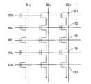
- FIG. 16 is a circuit diagram of a NAND nonvolatile semiconductor memory device.
- FIG. 6 is a graph showing the relationship between the charge amount at the time of writing and the film thickness of the tunnel insulating film. The figure which shows the energy band in 1st Embodiment.
- 10 (a) and 10 (b) are diagrams showing the electric field dependency in the tunnel insulating film regarding the amount of electron detrap and the amount of hole injection in the first embodiment.
- 11 (a) and 11 (b) are diagrams showing the film thickness dependency of the metal oxide film regarding the electron emission increase rate and the hole injection increase rate in the first embodiment.
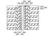
- FIG. 7 is a cross-sectional view showing a nonvolatile semiconductor memory device according to a second embodiment.
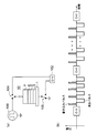
- FIG. 1 (a) shows an experimental apparatus
- FIG. 1 (b) shows a write pulse waveform, an erase pulse waveform, and a time series of CV measurement.
- a memory cell 10 having a structure in which a tunnel insulating film 3, a charge trap film 5, a block insulating film 6, and a control gate electrode 7 are stacked in this order is prepared on the semiconductor layer 1.
- a semiconductor layer means a well region formed on a semiconductor substrate, an SOI layer of an SOI (Silicon On Insulator) substrate, or a bulk semiconductor substrate.
- the CV measurement device 102 applies the initial state of the memory cell 10, that is, the write pulse and the erase pulse by switching the connection using the switch 104 and the switch 105. Measure the CV characteristics in the non-state. Thereafter, by switching the connection using the switch 104 and the switch 105, the write pulse and the erase pulse are repeatedly applied as a set from the pulse generator to the memory cell 10. Thereafter, the CV characteristic is measured by the CV measuring device 102 by switching the connection using the switch 104 and the switch 105. The application process of the write pulse and the erase pulse and the measurement process of the CV characteristic are repeated. As shown in FIG. 1B, the write pulse means that the pulse voltage applied to the memory cell is positive, and the erase pulse means that the pulse voltage is negative. Here, the experiment was performed by changing the width of the write pulse and the width of the erase pulse between 100 ⁇ sec and 100 msec. Further, in FIG. 1 (b), CV indicates a state in which the CV characteristic is measured.
- the CV stretch amount was calculated using the CV characteristic in the initial state obtained from the above experiment and the CV characteristic after repeated application of the write pulse and the erase pulse as one set.
- the CV stretch amount C-V stretch was calculated by the following equation.
- C-V stretch ⁇ V cycled - ⁇ V initial
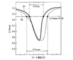
- ⁇ V initial is obtained from the CV characteristic of the initial state. Shows the C-V characteristics when normalized with a maximum capacity C max of C-V characteristics when this graph g 1 in FIG.
- the CV stretch amount C ⁇ V stretch indicates the interface state increase amount of the tunnel insulating film, that is, the degradation amount of the tunnel insulating film.
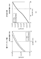
- FIGS. 3 (a) Show.
- a CV stretch quantity CV stretch showing the relationship between the cumulative amount Q era of erase pulses applied to the charge trapping layer in order to obtain this CV stretch quantity CV stretch in Figure 3 (b).
- the CV stretch amount C-V stretch is shown on the vertical axis.
- the horizontal axis of FIG. 3 (a) shows Q pgm
- the horizontal axis of FIG. 3 (b) shows Q era .
- FIG. 4 shows the electric field dependency of the current at the time of erasing.
- the white circles show the current values obtained by experiments, and the solid lines are the results calculated using equations (2) to (8) described later, assuming that the current is hole injection from the substrate. . Since the experimental values and calculated values are almost the same, it is considered that the erasing is almost performed by the hole injection. Therefore, the accumulated amount Q pgm shown in FIG. 3 (a) shows a nearly electrons accumulated amount accumulated amount Q era shown in FIG. 3 (b) shows a substantially holes accumulated amount. As can be seen from FIG. 3A, the CV stretch amount has no correlation with the integrated amount Q pgm . However, as can be seen from FIG. 3B, the CV stretch amount has a correlation with the integrated amount Q era . From these results, it is considered that the deterioration of the tunnel insulating film is determined by the amount of holes injected into the charge trap film.
- a nonvolatile semiconductor memory device provided with at least one memory cell 10 shown in FIG. 5 is provided.
- the memory cell 10 is provided on the semiconductor layer 1 to be the source region 2a and the drain region 2b provided separately in the semiconductor layer 1, and the channel 2c between the source region 2a and the drain region 2b.
- a region (interface region) 4 on the tunnel insulating film 3 side of the interface between the tunnel insulating film 3 and the charge trap film 5 includes metal atoms, and the metal atoms are mixed with oxygen of the tunnel insulating film 3 It is connected.
- this interface region 4 is very thin, but in the following description, the interface region 4 is also referred to as a metal oxide film 4 for the sake of convenience. That is, the metal oxide film 4 is a part of the tunnel insulating film 3.
- the block insulating film 6 blocks the charge from entering the control gate electrode 7 from the charge trapping film 5.
- the upper surface of the control gate electrode 7 and the side surfaces of the control gate electrode 7, the block insulating film 6, the charge trap film 5, the metal oxide film 4 and the tunnel insulating film are as follows. It is covered with a spacer film 8 of an insulator (for example, a silicon oxide film).
- FIGS. 6 (a) and 6 (b) Energy band diagrams of the charge holding state and the erasing state in the memory cell according to the present embodiment are shown in FIGS. 6 (a) and 6 (b), respectively.
- the barrier of the conduction band of the tunnel insulating film at the interface with the charge trap film 5 is modulated to lower the barrier to electrons (FIG. a), 6 (b)).
- the broken line indicates the barrier of the conduction band of the gate insulating film when no dipole is generated.
- the barrier to electrons is lowered, and electrons are more easily released from the charge trap film 5 to the semiconductor layer 1 through the metal oxide film 4 and the tunnel insulating film 3.
- the upper arrow indicates the emission of electrons from the charge trap film 5
- the lower arrow indicates the injection of holes to the charge trap film 5.
- the non-volatile semiconductor storage device is a NAND-type non-volatile semiconductor storage device, and has a plurality of memory cells M as shown in FIG.
- the plurality of memory cells 10 are connected in series such that adjacent ones share a source and a drain to form a NAND string.
- Such NAND strings are arranged in a matrix to form a memory cell array.
- the drains on one end side of the NAND series arranged in the column direction of the memory cell array are commonly connected to the bit line BL via the select transistor S1, and the other end side source is also a common source line (not shown) via the select transistor S2. Connected to).
- Control gates of the memory cells 10 aligned in the lateral direction shown in FIG. 7 are commonly connected to the word line WL.
- the gates of select transistors S1 and S2 are commonly connected to select gate lines SSL and GSL.
- a range of NAND series driven by one word line constitutes a NAND series block.
- a plurality of such NAND string blocks are arranged in the bit line direction to form a memory cell array.
- Each memory cell 10 is a MONOS type memory cell shown in FIG. That is, it comprises n-type source region 2a and drain region 2b containing n-type impurities (for example, P or As), which are formed apart from each other in p-type Si layer 1.
- a tunnel insulating film 3 including a silicon oxide film or a silicon oxynitride film is formed on Si layer 1 to be channel 2 c between source region 2 a and drain region 2 b, and metal oxide film 4 is formed on tunnel insulating film 3. Is formed.
- the metal oxide film 4 is an interface region on the tunnel insulating film 3 side of the interface between the tunnel insulating film 3 and the charge trapping film 5, and this interface region 4 contains metal atoms, Metal atoms are bonded to oxygen in the tunnel insulating film 3. That is, the metal oxide film 4 is a part of the tunnel insulating film 3.
- the charge trap film 5 is formed on the metal oxide film 4, the block insulating film 6 is formed on the charge trap film 5, and the control gate electrode 7 is formed on the block insulating film 6.
- the gate of the laminated structure including the control gate electrode 7, the block insulating film 6, the charge storage film 5, the metal oxide film 4, and the tunnel insulating film 3 is covered with the silicon oxide film 8.
- the metal oxide film 4 a material that forms a dipole in the direction from the charge trap film 5 to the tunnel insulating film 3, that is, positive charges exist on the charge trap film 5 side, and negative charges on the tunnel insulating film 3 side
- a material selected from the group consisting of Al 2 O 3 , HfO 2 , ZrO 2 , TiO 2 and MgO is used. That is, the metal oxide film 4 contains one element selected from the group of Al, Hf, Zr, Ti, and Mg.
- the tunnel insulating film may be a single layer film containing silicon oxide or silicon oxynitride. Also in this case, as described above, since the metal oxide film is the interface region of the tunnel insulating film, one metal atom selected from the group of Al, Hf, Zr, Ti, and Mg is the interface of the tunnel insulating film It is contained in the region and is combined with oxygen in the tunnel insulating film. In the case where the tunnel insulating film is a single layer film containing silicon oxynitride, it may have a nitrogen concentration distribution in the film thickness direction, either at the interface with the Si layer or at the interface with the charge trapping film 5. There may be a region not containing nitrogen.
- the nitrogen concentration [N] be [N] ⁇ 20 at% as an amount capable of ensuring the deterioration resistance of the tunnel insulating film and capable of generating a dipole.
- a SiO 2 film is formed with a transition layer of about 0.6 nm between the Si substrate (Si layer) and other oxides, and this transition layer is poor in film quality, so in addition to the upper and lower SiO 2 transition layers. It is desirable to have a film thickness of 1.8 nm or more, further adding 0.6 nm or more.
- the threshold voltage shift amount ⁇ V th of the memory cell 10 is 7 V
- the charge amount Q trap which has to be captured in the charge trap film 5 at the time of write and erase operation is from the Si substrate 1 to the charge center position.
- ⁇ ox represents the dielectric constant of SiO 2
- ⁇ Vth represents the shift amount of the threshold voltage.
- a silicon oxide film / silicon nitride film (SiN film) / alumina (Al 2 O 3 ) film is used as a stacked structure of tunnel insulating film / charge trap film / block insulating film in a typical MONOS structure, and the write and erase operation is performed.
- the charge center position of the charge injected by is calculated at the interface between the SiN film and the Al 2 O 3 film with reference to known documents (S. Fujii et al. SSDM 2009)
- FIG. 8 shows the film thickness dependency of the amount of charge that can be written in 100 ⁇ sec.
- the voltage applied to the control gate electrode 7 is 20 V
- the thickness of the block insulating film 6 is 13 nm
- the thickness of the charge trap film 5 is 5 nm.
- the injection charge amount Q 5 ⁇ 10 ⁇ 6 [C / cm 2 ] can not be secured, so the film thickness of the tunnel insulating film 3 is less than 5 nm. It is desirable to have.
- a p-type Si layer is used as the semiconductor layer 1, a silicon oxide film as the tunnel insulating film 3, an Al 2 O 3 film as the metal oxide film 4 for forming a dipole, and Si 3 as the charge trap film 5.
- An N 4 membrane is used. It is known that the level of electrons captured by the Si 3 N 4 film 5 to be a charge trapping film is at a position of 1.3 eV from the conduction band of Si.
- the modulation amount of the band depends on the film thickness of the inserted Al 2 O 3 film, and the film thickness of the Al 2 O 3 film is 0.2 eV and 0.4 eV, and the film thickness of the Al 2 O 3 film is 0.5 eV at 0.5 nm, 0.58 eV at 1 nm, and 0.6 eV at 1.5 nm or more.
- the Al 2 O 3 film 4 It is considered that only a dipole is formed at the interface between the SiO 2 film 3 and the Si 3 N 4 film 5 without being present as a bulk, and it is considered as a band diagram as shown in FIG.
- the leak current was calculated on the assumption that the Al 2 O 3 film 4 had bulk properties.
- the film thickness of the tunnel insulating film 3 is T 1
- the film thickness of the metal oxide film 4 is T 2 .
- the leakage current passing through the tunnel insulating film 3 is calculated, and the amount of electron emission and the amount of hole injection are determined.
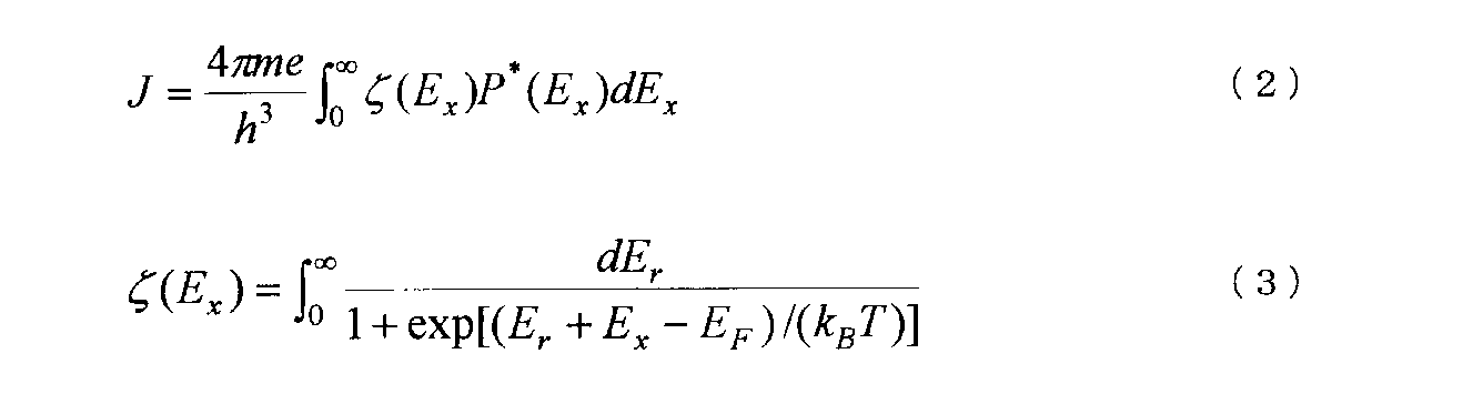
- the leakage current was calculated by using the following equations (2) and (3).
- e is an elementary charge
- m is the mass of electrons in vacuum
- h Planck's constant
- k B is Boltzmann's constant
- T absolute temperature
- the effective mass was 0.5 m as a typical value.
- m is the mass of the electron in vacuum.
- the FN tunnel means a tunnel in which electrons pass through the inclined conduction band of the insulating film.
- the tunnel probability can be expressed by a combination of this FN tunnel probability as shown in equation
- the oxide film electric field dependency of the electron emission amount Je and the hole injection amount Jh is calculated.
- a) and 10 (b) are shown by solid lines, respectively.
- the case where the tunnel insulating film is formed of a single layer of SiO 2 film is shown by a wavy line for comparison.
- electrons detrapped from the charge storage layer are trapped in the storage film and are in a bound state, but in the calculation, both electrons and holes are treated as free electrons and free holes. As can be seen from FIGS.
- the horizontal axis indicates the film thickness of Al 2 O 3
- black circles indicate simulation results
- white circles indicate extrapolated points.
- the rate of erasing by electron detrapping with respect to erasing by hole injection is larger when metal oxide film 4 is inserted, and thus the same erasing characteristics are obtained.
- the amount of hole injection can be reduced, and the deterioration of the tunnel insulating film 4 can be suppressed.
- the film thickness of the Al 2 O 3 film 4 is less than the lattice constant (0.47 nm) means that the surface density of Al is less than 2.2 ⁇ 10 15 atoms / cm 2.
- HfO 2 , MgO, TiO 2 or ZrO 2 can be used as the metal oxide film 4 in addition to Al 2 O 3 .
- the charge trapping film is hafnia (HfO 2 film)
- a material whose dipole is larger than that of HfO 2 for example, Al 2 O 3 , TiO 2 , or ZrO 2 can be used as the metal oxide film 4.
- the upper limit of the film thickness of the metal oxide film 4 for suppressing the deterioration of the tunnel insulating film 3 can be obtained from the lattice constant of each material.
- the lattice constant of HfO 2 is 0.51 nm
- the lattice constant of MgO is 0.41 nm
- the lattice constant of TiO 2 is 0.46 nm
- the lattice constant of ZrO 2 is 0.52 nm.
- the upper limit of the film thickness of the metal oxide film 4 when HfO 2 , MgO, TiO 2 or ZrO 2 is used is 0.51 nm, 0.41 nm, 0.46 nm or 0.52 nm, respectively.
- Hf is 1.3 ⁇ 10 15 atoms / cm 2
- Mg is 2.2 ⁇ 10 15 atoms / cm 2
- Ti is 2.9 ⁇ 10 15 atoms.
- / Cm 2 and Zr is less than 1.5 ⁇ 10 15 atoms / cm 2 .
- the metal oxide film can be deposited by a sputtering method, an ALD method, or a CVD method.
- the erasure due to the electron detrapping can be promoted, and the deterioration of the tunnel insulating film caused by the writing and erasure stress can be suppressed.
- the nonvolatile semiconductor memory device of this embodiment is a MONOS semiconductor memory having a stacked structure in which a control gate made of doped polysilicon or the like and an interlayer insulating film made of a silicon oxide film or the like are deposited in multiple layers. A plurality of memory cells are provided.
- the nonvolatile semiconductor memory device of this embodiment has a stacked structure 200 in which a control gate 202 made of doped polysilicon and the like and an interlayer insulating film 203 made of a silicon oxide film and the like are multiply deposited on a substrate (not shown). (FIG. 12).
- the stacked structure 200 is provided with an opening 204 provided along the stacking direction.
- a block insulating film 205 made of a high dielectric constant insulating film or a silicon oxide film is formed on the inner wall of the opening 204.
- a silicon nitride film to be the charge trapping film 206 is formed so as to cover the surface on the inner side (the opposite side to the laminated structure 200) of the block insulating film 205 formed on the inner wall of the opening 204.
- a metal oxide film 207 such as an Al 2 O 3 film, is formed to cover the surface inside silicon nitride film 206 (the opposite side to block insulating film 205).
- a tunnel insulating film 208 is formed to cover the inner surface (the opposite side to the silicon nitride film 207) of the metal oxide film 207.
- the metal oxide film 207 is very thin, and is formed in a region (interface region) on the tunnel insulating film 208 side of the interface between the tunnel insulating film 208 and the charge trapping film 206. And a metal atom, which is bonded to oxygen of the tunnel insulating film 208. Therefore, the metal oxide film 207 is included in the tunnel insulating film 208.
- the tunnel insulating film 208 may be a single layer of a silicon oxide film or a single layer of a silicon oxynitride film.
- nitrogen may have a concentration distribution in the film thickness direction, and nitrogen is present at the interface with the semiconductor layer 208 or the interface with the charge trapping film 206 described later. There may be areas not included.
- a semiconductor layer 209 serving as a channel is formed to cover the surface on the inner side (the opposite side to the metal oxide film 207) of the tunnel insulating film 208.
- the metal oxide film 207 is a material that forms a dipole in the direction from the charge trap film 206 to the tunnel insulating film 208, that is, positive charges are present on the charge trap film 206 side and negative on the tunnel insulating film 208 side.
- a material in which a charge is present such as a material selected from the group of Al 2 O 3 , HfO 2 , ZrO 2 , TiO 2 , MgO, is used. That is, the metal oxide film 207 contains one element selected from the group of Al, Hf, Zr, Ti, and Mg.
- the thickness of the metal oxide film 207 is preferably larger than 0 and less than the lattice constant of the material of the metal oxide film 207, as in the first embodiment.
- the nonvolatile semiconductor memory device of this embodiment configured in this way is a semiconductor memory device having a three-dimensional structure, and, as in the first embodiment, between the tunnel insulating film 208 and the charge trap film 206. Since the metal oxide film 207 is provided, a dipole is generated at the interface between the tunnel insulating film 208 and the metal oxide film 208. Thus, as in the first embodiment, the erasure due to the emission of electrons is promoted, and the deterioration of the tunnel insulating film can be suppressed.
- the film thickness of the metal oxide film 4 is greater than 0 and less than the lattice constant of the material forming the metal oxide film 4. That is, the metal oxide film 4 is an interface region 4 on the tunnel insulating film 3 side of the interface between the tunnel insulating film 3 and the charge trap film 5, and the interface region 4 contains metal atoms, and the metal atoms are tunneled.
- the oxygen is combined with the insulating film 3 to form a dipole. That is, at the interface between tunnel insulating film 3 and charge trap film 5, at least one metal atom selected from the group of Al, Hf, Zr, Ti, Mg is present, and this metal atom is diffused into charge trap film 5. It may be done.
- nonvolatile semiconductor memory device having a three-dimensional structure for example, a fin-type nonvolatile semiconductor memory layer, a nanowire-type nonvolatile semiconductor memory device, Japanese Patent Laid-Open No. 2007-266143.
- the present invention can also be applied to the non-volatile semiconductor memory device described, or to the three-dimensionally stacked non-volatile semiconductor memory device shown in R. Katsumata et al., 2009, VLSI symp. P 136.
Landscapes
- Semiconductor Memories (AREA)
- Non-Volatile Memory (AREA)
Abstract
Description
C-Vstretch = ΔVcycled -ΔVinitial
ここで、ΔVinitialは初期状態のC-V特性から求められる。この時のC-V特性を最大容量Cmaxで正規化した場合のC-V特性を図2のグラフg1に示す。ここで通常のMONOS構造におけるVfbは、Cmaxの80%~90%となる電圧となるため、初期状態の正規化されたC-V特性g1において、C/Cmax=0.85の時の、電荷を蓄積する際のゲート電圧と、反転する(電荷を放出する)際のゲート電圧との差をΔVinitialとして求めた(図2のグラフg1参照)。また、ΔVcycledは書き込みパルスおよび消去パルスを繰り返して印加した場合のC-V特性から求められる。この時のC-V特性を最大容量Cmaxで正規化した場合のC-V特性を図2のグラフg2に示す。この正規化されたC-V特性g2において、C/Cmax=0.85の時の蓄積する際のゲート電圧と、反転する際のゲート電圧との差をΔVinitialとして求めた(図2のグラフg2参照)。したがって、CVストレッチ量C-Vstretchはトンネル絶縁膜の界面準位増加量、すなわちトンネル絶縁膜の劣化量を示している。
次に、本発明の第1実施形態による不揮発性半導体記憶装置は、NAND型不揮発性半導体記憶装置であって、図7に示すように、複数のメモリセルMを有している。これらの複数のメモリセル10は、隣接するもの同士でソースおよびドレインを共有する形で直列接続されてNAND列を構成する。このようなNAND列がマトリクス状に配列されてメモリセルアレイが構成される。

以下に本実施形態の一実施例を説明する。この実施例では、半導体層1としてp型Si層を、トンネル絶縁膜3としてシリコン酸化膜を、ダイポールを形成するための金属酸化膜4としてAl2O3膜を、電荷トラップ膜5としてSi3N4膜を用いている。電荷トラップ膜となるSi3N4膜5に捕獲された電子の準位はSiの伝導帯から1.3eVの位置にあることがわかっている。また、Al2O3膜をSiO2膜とSi3N4膜との界面に挿入すると、ダイポールが生成され、SiO2の電子に対するバンドオフセットが下がることが報告されている(例えば、IEDM2007 Y.Kamimuta et al参照)。ここで、バンドの変調量は、挿入されたAl2O3膜の膜厚に依存し、Al2O3膜の膜厚が0.2nmで0.4eV、Al2O3膜の膜厚が0.5nmで0.5eV、1nmで0.58eV、1.5nm以上では0.6eVである。
εoxEox=ε1E1=ε2E2 (4)
となる。ここで、εox(=3.9)はSiO2の誘電率である。なお、実電界E1、E2は、
E1=V1/T1、 E2=V2/T2 (5)
と定義した。


TFN(φb *,m*,E)=1 (8)
で定義される。ここで、m*はトンネル絶縁膜中をトンネルしている電子の有効質量、φb *はトンネル絶縁膜の実効的なバリアハイト、EFはフェルミレベル、Exは電子のトンネル方向のエネルギー、eは素電荷、hはプランク定数、E1およびE2はそれぞれトンネル絶縁膜3および金属酸化膜4における実電界を示す。なお、F-Nトンネルとは、電子が絶縁膜の傾斜した伝導帯を通り抜けるトンネルを意味する。トンネル確率は、(5)式に示すように、このF-Nトンネル確率の組み合わせで表現できる。
次に、本発明の第2実施形態による不揮発性半導体記憶装置を図12に示す。本実施形態の不揮発性半導体記憶装置は、ドーピングされたポリシリコンなどからなる制御ゲートと、シリコン酸化膜などからなる層間絶縁膜を多重に堆積させた積層構造を有するMONOS型の半導体メモリあって、複数のメモリセルを備えている。
2a ソース領域
2b ドレイン領域
3 トンネル絶縁膜
4 金属酸化膜(界面領域)
5 電荷トラップ膜
6 ブロック絶縁膜
7 制御ゲート電極
8 スペーサ膜
10 メモリセル
200 積層構造
202 制御ゲート
203 層間絶縁膜
204 開口
205 ブロック絶縁膜
206 電荷トラップ膜
207 金属酸化膜
208 トンネル絶縁膜
209 半導体層(チャネル)
Claims (6)
- 半導体層と、
前記半導体層上に形成され、酸化シリコンまたは酸窒化シリコンを含む単層膜からなる第1絶縁膜と、
前記第1絶縁膜上に形成された電荷トラップ膜と、
前記電荷トラップ膜上に形成された第2絶縁膜と、
前記第2絶縁膜上に形成された制御ゲート電極と、
を備え、前記第1絶縁膜と前記電荷トラップ膜との界面に、Al、Hf、Zr、Ti、Mgのグループから選択された金属原子が存在していることを特徴とする不揮発性半導体記憶装置。 - 前記トンネル絶縁膜の界面領域における前記金属原子の面密度は、前記金属原子がHfの場合は1.3×10¹⁵atomic/cm2未満であり、Mgの場合は2.2×1015atomic/cm2未満であり、Tiの場合は2.9×1015atomic/cm2未満であり、Zrの場合は1.5×1015atomic/cm2未満であることを特徴とする請求項1記載の不揮発性半導体記憶装置。
- 前記第1絶縁膜はシリコン酸化膜であり、膜厚が1.8nm以上5nm未満であることを特徴とする請求項1記載の不揮発性半導体記憶装置。
- 前記第1絶縁膜はシリコン酸窒化膜であり、このシリコン酸窒化膜の窒素濃度が20at%未満であることを特徴とする請求項1記載の不揮発性半導体記憶装置。
- 前記電荷トラップ膜はシリコン窒化膜であることを特徴とする請求項1記載の不揮発性半導体記憶装置。
- 前記電荷トラップ膜はハフニアであり、前記金属原子はAl、Zr、Tiのグループから選択されることを特徴とする請求項1記載の不揮発性半導体記憶装置。
Priority Applications (4)
| Application Number | Priority Date | Filing Date | Title |
|---|---|---|---|
| KR1020127010700A KR20120054660A (ko) | 2009-11-04 | 2009-11-04 | 불휘발성 반도체 기억 장치 |
| JP2011539219A JPWO2011055433A1 (ja) | 2009-11-04 | 2009-11-04 | 不揮発性半導体記憶装置 |
| PCT/JP2009/068845 WO2011055433A1 (ja) | 2009-11-04 | 2009-11-04 | 不揮発性半導体記憶装置 |
| US13/457,054 US8698313B2 (en) | 2009-11-04 | 2012-04-26 | Nonvolatile semiconductor memory apparatus |
Applications Claiming Priority (1)
| Application Number | Priority Date | Filing Date | Title |
|---|---|---|---|
| PCT/JP2009/068845 WO2011055433A1 (ja) | 2009-11-04 | 2009-11-04 | 不揮発性半導体記憶装置 |
Related Child Applications (1)
| Application Number | Title | Priority Date | Filing Date |
|---|---|---|---|
| US13/457,054 Continuation US8698313B2 (en) | 2009-11-04 | 2012-04-26 | Nonvolatile semiconductor memory apparatus |
Publications (1)
| Publication Number | Publication Date |
|---|---|
| WO2011055433A1 true WO2011055433A1 (ja) | 2011-05-12 |
Family
ID=43969678
Family Applications (1)
| Application Number | Title | Priority Date | Filing Date |
|---|---|---|---|
| PCT/JP2009/068845 Ceased WO2011055433A1 (ja) | 2009-11-04 | 2009-11-04 | 不揮発性半導体記憶装置 |
Country Status (4)
| Country | Link |
|---|---|
| US (1) | US8698313B2 (ja) |
| JP (1) | JPWO2011055433A1 (ja) |
| KR (1) | KR20120054660A (ja) |
| WO (1) | WO2011055433A1 (ja) |
Cited By (9)
| Publication number | Priority date | Publication date | Assignee | Title |
|---|---|---|---|---|
| JP2012248691A (ja) * | 2011-05-27 | 2012-12-13 | Toshiba Corp | 不揮発性半導体記憶装置及びその製造方法 |
| JP2014053428A (ja) * | 2012-09-06 | 2014-03-20 | Toshiba Corp | 半導体装置及びその製造方法 |
| JP2015060911A (ja) * | 2013-09-18 | 2015-03-30 | 独立行政法人産業技術総合研究所 | 不揮発性記憶素子 |
| JP2016535932A (ja) * | 2013-11-08 | 2016-11-17 | ユ−ジーン テクノロジー カンパニー.リミテッド | サイクリック薄膜蒸着方法及び半導体製造方法及び半導体素子 |
| US9741400B2 (en) | 2015-11-05 | 2017-08-22 | Semiconductor Energy Laboratory Co., Ltd. | Semiconductor device, memory device, electronic device, and method for operating the semiconductor device |
| US9768265B1 (en) | 2016-03-17 | 2017-09-19 | Toshiba Memory Corporation | Semiconductor memory device |
| JP2020064897A (ja) * | 2018-10-15 | 2020-04-23 | 国立研究開発法人産業技術総合研究所 | 不揮発性記憶素子 |
| KR20210024987A (ko) * | 2020-09-09 | 2021-03-08 | 에스케이하이닉스 주식회사 | 반도체 장치 및 반도체 장치의 제조 방법 |
| US11201214B2 (en) | 2019-08-26 | 2021-12-14 | SK Hynix Inc. | Semiconductor device and manufacturing method of the semiconductor device |
Families Citing this family (8)
| Publication number | Priority date | Publication date | Assignee | Title |
|---|---|---|---|---|
| JP2015177129A (ja) * | 2014-03-17 | 2015-10-05 | 株式会社東芝 | 半導体記憶装置及びその製造方法 |
| US9449980B2 (en) * | 2014-10-31 | 2016-09-20 | Sandisk Technologies Llc | Band gap tailoring for a tunneling dielectric for a three-dimensional memory structure |
| US10134750B2 (en) * | 2014-12-30 | 2018-11-20 | Toshiba Memory Corporation | Stacked type semiconductor memory device and method for manufacturing the same |
| US10325918B2 (en) * | 2016-11-29 | 2019-06-18 | Taiwan Semiconductor Manufacturing Co., Ltd. | Semiconductor device and manufacturing method thereof |
| US10381431B2 (en) | 2017-10-30 | 2019-08-13 | International Business Machines Corporation | Artificial synapse with hafnium oxide-based ferroelectric layer in CMOS back-end |
| US10319818B2 (en) | 2017-10-30 | 2019-06-11 | International Business Machines Corporation | Artificial synapse with hafnium oxide-based ferroelectric layer in CMOS front-end |
| US10720444B2 (en) * | 2018-08-20 | 2020-07-21 | Sandisk Technologies Llc | Three-dimensional flat memory device including a dual dipole blocking dielectric layer and methods of making the same |
| JP2024001641A (ja) * | 2022-06-22 | 2024-01-10 | キオクシア株式会社 | 半導体装置及びその製造方法 |
Citations (5)
| Publication number | Priority date | Publication date | Assignee | Title |
|---|---|---|---|---|
| JP2004103902A (ja) * | 2002-09-11 | 2004-04-02 | Sony Corp | 不揮発性半導体メモリ装置、および、その製造方法 |
| JP2006324351A (ja) * | 2005-05-17 | 2006-11-30 | Nippon Telegr & Teleph Corp <Ntt> | 電荷蓄積型メモリ |
| JP2009081203A (ja) * | 2007-09-25 | 2009-04-16 | Toshiba Corp | 不揮発性半導体記憶装置およびその製造方法 |
| JP2009212321A (ja) * | 2008-03-05 | 2009-09-17 | Nippon Telegr & Teleph Corp <Ntt> | 半導体メモリ |
| JP2009231373A (ja) * | 2008-03-19 | 2009-10-08 | Toshiba Corp | 不揮発性半導体記憶装置 |
Family Cites Families (11)
| Publication number | Priority date | Publication date | Assignee | Title |
|---|---|---|---|---|
| US7595528B2 (en) * | 2004-03-10 | 2009-09-29 | Nanosys, Inc. | Nano-enabled memory devices and anisotropic charge carrying arrays |
| US7504700B2 (en) * | 2005-04-21 | 2009-03-17 | International Business Machines Corporation | Method of forming an ultra-thin [[HfSiO]] metal silicate film for high performance CMOS applications and semiconductor structure formed in said method |
| JP4928890B2 (ja) | 2005-10-14 | 2012-05-09 | 株式会社東芝 | 不揮発性半導体記憶装置 |
| JP5016832B2 (ja) | 2006-03-27 | 2012-09-05 | 株式会社東芝 | 不揮発性半導体記憶装置及びその製造方法 |
| JP4908238B2 (ja) * | 2007-01-11 | 2012-04-04 | 株式会社東芝 | 不揮発性半導体記憶装置 |
| JP4594973B2 (ja) | 2007-09-26 | 2010-12-08 | 株式会社東芝 | 不揮発性半導体記憶装置 |
| US20090242956A1 (en) * | 2008-03-28 | 2009-10-01 | Heng Jiunn B | Tunnel dielectrics for semiconductor devices |
| JP5416936B2 (ja) * | 2008-09-02 | 2014-02-12 | 株式会社東芝 | 半導体装置およびその製造方法 |
| JP5361294B2 (ja) | 2008-09-04 | 2013-12-04 | 株式会社東芝 | 不揮発性半導体記憶装置 |
| JP5472894B2 (ja) | 2008-09-25 | 2014-04-16 | 株式会社東芝 | 不揮発性半導体記憶装置 |
| KR101155108B1 (ko) * | 2009-04-30 | 2012-06-11 | 국민대학교산학협력단 | 전하저장층 및 그의 형성 방법, 이를 이용한 비휘발성 메모리 장치 및 그의 제조 방법 |
-
2009
- 2009-11-04 KR KR1020127010700A patent/KR20120054660A/ko not_active Abandoned
- 2009-11-04 WO PCT/JP2009/068845 patent/WO2011055433A1/ja not_active Ceased
- 2009-11-04 JP JP2011539219A patent/JPWO2011055433A1/ja active Pending
-
2012
- 2012-04-26 US US13/457,054 patent/US8698313B2/en active Active
Patent Citations (5)
| Publication number | Priority date | Publication date | Assignee | Title |
|---|---|---|---|---|
| JP2004103902A (ja) * | 2002-09-11 | 2004-04-02 | Sony Corp | 不揮発性半導体メモリ装置、および、その製造方法 |
| JP2006324351A (ja) * | 2005-05-17 | 2006-11-30 | Nippon Telegr & Teleph Corp <Ntt> | 電荷蓄積型メモリ |
| JP2009081203A (ja) * | 2007-09-25 | 2009-04-16 | Toshiba Corp | 不揮発性半導体記憶装置およびその製造方法 |
| JP2009212321A (ja) * | 2008-03-05 | 2009-09-17 | Nippon Telegr & Teleph Corp <Ntt> | 半導体メモリ |
| JP2009231373A (ja) * | 2008-03-19 | 2009-10-08 | Toshiba Corp | 不揮発性半導体記憶装置 |
Cited By (13)
| Publication number | Priority date | Publication date | Assignee | Title |
|---|---|---|---|---|
| JP2012248691A (ja) * | 2011-05-27 | 2012-12-13 | Toshiba Corp | 不揮発性半導体記憶装置及びその製造方法 |
| US8987804B2 (en) | 2011-05-27 | 2015-03-24 | Kabushiki Kaisha Toshiba | Nonvolatile semiconductor memory device and method of fabricating the same |
| JP2014053428A (ja) * | 2012-09-06 | 2014-03-20 | Toshiba Corp | 半導体装置及びその製造方法 |
| US9087910B2 (en) | 2012-09-06 | 2015-07-21 | Kabushiki Kaisha Toshiba | Semiconductor device and manufacturing method of the same |
| JP2015060911A (ja) * | 2013-09-18 | 2015-03-30 | 独立行政法人産業技術総合研究所 | 不揮発性記憶素子 |
| JP2016535932A (ja) * | 2013-11-08 | 2016-11-17 | ユ−ジーン テクノロジー カンパニー.リミテッド | サイクリック薄膜蒸着方法及び半導体製造方法及び半導体素子 |
| US9741400B2 (en) | 2015-11-05 | 2017-08-22 | Semiconductor Energy Laboratory Co., Ltd. | Semiconductor device, memory device, electronic device, and method for operating the semiconductor device |
| US9768265B1 (en) | 2016-03-17 | 2017-09-19 | Toshiba Memory Corporation | Semiconductor memory device |
| JP2020064897A (ja) * | 2018-10-15 | 2020-04-23 | 国立研究開発法人産業技術総合研究所 | 不揮発性記憶素子 |
| JP7145495B2 (ja) | 2018-10-15 | 2022-10-03 | 国立研究開発法人産業技術総合研究所 | 不揮発性記憶素子 |
| US11201214B2 (en) | 2019-08-26 | 2021-12-14 | SK Hynix Inc. | Semiconductor device and manufacturing method of the semiconductor device |
| KR20210024987A (ko) * | 2020-09-09 | 2021-03-08 | 에스케이하이닉스 주식회사 | 반도체 장치 및 반도체 장치의 제조 방법 |
| KR102245781B1 (ko) | 2020-09-09 | 2021-04-28 | 에스케이하이닉스 주식회사 | 반도체 장치 및 반도체 장치의 제조 방법 |
Also Published As
| Publication number | Publication date |
|---|---|
| KR20120054660A (ko) | 2012-05-30 |
| US20120261742A1 (en) | 2012-10-18 |
| JPWO2011055433A1 (ja) | 2013-03-21 |
| US8698313B2 (en) | 2014-04-15 |
Similar Documents
| Publication | Publication Date | Title |
|---|---|---|
| US8698313B2 (en) | Nonvolatile semiconductor memory apparatus | |
| JP4923318B2 (ja) | 不揮発性半導体記憶装置およびその動作方法 | |
| JP5149539B2 (ja) | 半導体装置 | |
| JP5154841B2 (ja) | 不揮発性メモリデバイスの製造方法 | |
| CN1828944B (zh) | 非易失性存储单元及具有非易失性存储单元的存储器阵列 | |
| JP2008217972A (ja) | 不揮発性メモリ素子の作動方法 | |
| JP5238208B2 (ja) | 不揮発性半導体記憶装置の駆動方法及び不揮発性半導体記憶装置 | |
| US8975687B2 (en) | Nonvolatile memory array with continuous charge storage dielectric stack | |
| KR100706071B1 (ko) | 단일비트 비휘발성 메모리셀 및 그것의 프로그래밍 및삭제방법 | |
| US20070297244A1 (en) | Top Dielectric Structures in Memory Devices and Methods for Expanding a Second Bit Operation Window | |
| JP2006339599A (ja) | 半導体装置およびその製造方法 | |
| Kim et al. | Paired FinFET charge trap flash memory for vertical high density storage | |
| KR100684900B1 (ko) | 비휘발성 기억 소자 및 그 동작 방법 | |
| KR101281683B1 (ko) | 전하 트랩형 플래시 메모리 소자의 작동 방법 | |
| US7599229B2 (en) | Methods and structures for expanding a memory operation window and reducing a second bit effect | |
| Yu et al. | Perspective of flash memory realized on vertical Si nanowires | |
| US20130320425A1 (en) | Nonvolatile semiconductor memory device | |
| CN100470810C (zh) | 扩展第二位元操作裕度的存储器结构 | |
| CN104425503B (zh) | 非易失性半导体存储器件及其制造方法和制造装置 | |
| KR100868031B1 (ko) | 비휘발성 메모리 소자 및 이를 제조하는 방법 | |
| KR101601101B1 (ko) | 전하 트랩을 이용한 메모리 소자 및 그의 제조 방법 | |
| Lee et al. | Retention reliability of finFET SONOS device | |
| CN100372121C (zh) | 多阶存储单元 | |
| KR101244842B1 (ko) | 전하 트랩형 플래시 메모리 소자의 작동 방법 | |
| US20080121980A1 (en) | Bottom Dielectric Structures and High-K Memory Structures in Memory Devices and Methods for Expanding a Second Bit Operation Window |
Legal Events
| Date | Code | Title | Description |
|---|---|---|---|
| 121 | Ep: the epo has been informed by wipo that ep was designated in this application |
Ref document number: 09851086 Country of ref document: EP Kind code of ref document: A1 |
|
| WWE | Wipo information: entry into national phase |
Ref document number: 2011539219 Country of ref document: JP |
|
| ENP | Entry into the national phase |
Ref document number: 20127010700 Country of ref document: KR Kind code of ref document: A |
|
| NENP | Non-entry into the national phase |
Ref country code: DE |
|
| 122 | Ep: pct application non-entry in european phase |
Ref document number: 09851086 Country of ref document: EP Kind code of ref document: A1 |