WO2011048746A1 - 磁気転写用原盤の製造方法 - Google Patents
磁気転写用原盤の製造方法 Download PDFInfo
- Publication number
- WO2011048746A1 WO2011048746A1 PCT/JP2010/005618 JP2010005618W WO2011048746A1 WO 2011048746 A1 WO2011048746 A1 WO 2011048746A1 JP 2010005618 W JP2010005618 W JP 2010005618W WO 2011048746 A1 WO2011048746 A1 WO 2011048746A1
- Authority
- WO
- WIPO (PCT)
- Prior art keywords
- layer
- magnetic transfer
- magnetic
- etching
- substrate
- Prior art date
- Legal status (The legal status is an assumption and is not a legal conclusion. Google has not performed a legal analysis and makes no representation as to the accuracy of the status listed.)
- Ceased
Links
Images



Classifications
-
- G—PHYSICS
- G11—INFORMATION STORAGE
- G11B—INFORMATION STORAGE BASED ON RELATIVE MOVEMENT BETWEEN RECORD CARRIER AND TRANSDUCER
- G11B5/00—Recording by magnetisation or demagnetisation of a record carrier; Reproducing by magnetic means; Record carriers therefor
- G11B5/86—Re-recording, i.e. transcribing information from one magnetisable record carrier on to one or more similar or dissimilar record carriers
- G11B5/865—Re-recording, i.e. transcribing information from one magnetisable record carrier on to one or more similar or dissimilar record carriers by contact "printing"
Definitions
- the present invention relates to a method of manufacturing a master for magnetic transfer for magnetically transferring information to a magnetic recording medium.
- a magnetic disk used for a hard disk drive is written with various magnetic information such as format information, address information, and servo information before being incorporated into the drive.
- magnetic information is written using a magnetic head.
- a magnetic transfer method has been proposed in which magnetic information is collectively written on a magnetic disk.
- a master disk (master disk) having a magnetic layer formed according to a magnetic information recording pattern is used.
- a master disk (master disk) and a disk to be transferred (slave disk) are in close contact with each other, and an external magnetic field generated by an electromagnet or permanent magnet is applied from one or both sides to face the magnetic layer.
- the area on the slave disk to be magnetized is collectively magnetized.
- Patent Document 1 a substrate having a concavo-convex pattern corresponding to information to be transferred is formed on the surface, and a metal plate is manufactured by electroforming the surface of the substrate. Describes a method for producing a master carrier for magnetic transfer in which the substrate is peeled off from the surface of the substrate.
- Patent Document 1 and Patent Document 2 since the method described in Patent Document 1 and Patent Document 2 includes a step of peeling the metal disk produced by the electroforming method from the substrate, the metal disk may be warped by the stress at the time of peeling. Therefore, with these methods, it is difficult to form a magnetic layer pattern with high accuracy, and it is also very difficult to improve the transfer accuracy of magnetic information.
- an object of the present invention is to provide a method of manufacturing a master for magnetic transfer capable of forming a magnetic layer pattern with high accuracy.
- a method for manufacturing a master for magnetic transfer includes a step of forming a magnetic transfer layer containing at least one of iron and cobalt on a substrate.
- a mask pattern is formed on the magnetic transfer layer.
- the magnetic transfer layer is etched through the mask pattern by holding the substrate at a temperature of 100 ° C. or higher and forming plasma of chlorine-based gas.
- a method for manufacturing a master for magnetic transfer includes a step of forming a magnetic transfer layer containing at least one of iron (Fe) and cobalt (Co) on a substrate.
- a mask pattern is formed on the magnetic transfer layer.
- the magnetic transfer layer is etched through the mask pattern by holding the substrate at a temperature of 100 ° C. or higher and forming plasma of chlorine-based gas.
- the magnetic transfer layer on the substrate is chemically etched by reactive ion etching (RIE) using chlorine-based gas plasma.
- RIE reactive ion etching
- the etching rate of the magnetic transfer layer may be low, which may impair productivity.
- the substrate temperature has no particular upper limit, but the upper limit can be appropriately determined according to the heat resistance of each layer including the magnetic transfer layer.
- the magnetic transfer layer can be composed of a single metal or an alloy such as Fe, Fe-based alloy, Co, Co-based alloy, and FeCo-based alloy. Besides this, an artificial lattice such as FeCo / Pd is also applicable. .
- etching gas for the magnetic transfer layer a chlorine-based gas such as Cl 2 , BCl 3 , or SiCl 4 is used.
- a method for forming plasma is not particularly limited, and inductively coupled plasma, capacitively coupled plasma, magnetic field inductively coupled plasma, electron cyclotron resonance plasma, and the like are applicable.
- the substrate temperature during etching can be typically adjusted using a heating source.
- the mask pattern can be made of chromium (Cr) or ruthenium (Ru). Ru and Cr constituting the mask pattern are not etched only by the chlorine-based gas, but are etched by adding oxygen to the chlorine-based gas. In other words, etching progresses by generating RuO 4 in Ru and CrO 2 Cl 2 in Cr. A Ru or Cr mask is formed using such a gas, and the magnetic transfer layer is etched using only a chlorine-based gas, so that a sufficient selectivity with Ru or Cr can be obtained and a good etching pattern can be formed. be able to.
- a fluorine-based gas can be used as the etching gas for the mask pattern.
- the method for manufacturing the master for magnetic transfer may further include a step of forming an intermediate layer having etching resistance against the plasma of the chlorine-based gas on the substrate before forming the magnetic transfer layer. Good. Thereby, it is possible to avoid an adverse effect of the plasma on the substrate during the overetching of the magnetic transfer layer.
- the intermediate layer can also function as an adhesion layer between the substrate and the magnetic transfer layer. Examples of the material constituting such an intermediate layer include Ru, Cr, Ni, and the like.
- the method for manufacturing the master for magnetic transfer may further include a step of cleaning the magnetic transfer layer after etching the magnetic transfer layer. Since the Fe and Co chlorides are water-soluble, the etching reaction product formed on the surface of the magnetic transfer layer can be removed by washing the substrate after etching.
- the cleaning liquid pure water, ion exchange water, micro / nano bubble water, and various organic solvents can be used. Examples of the organic solvent include ethanol, methanol, acetone, isopropyl alcohol, and ethyl ether.
- the substrate 11 is composed of a flat disk (disc) substrate.
- the substrate 11 is composed of, for example, a silicon substrate, a glass substrate, a ceramic substrate, or the like.
- the thickness of the substrate 11 is not particularly limited, and can be set as appropriate as long as an appropriate rigidity without warping or distortion is obtained.
- the magnetic layer pattern 12P is made of a ferromagnetic material.
- Typical examples of the ferromagnetic material include ferromagnetic materials having soft magnetic properties such as Fe-based materials, Co-based materials, and FeCo-based materials. Metalloid elements such as B, P, and Si may be added.
- Examples of the ferromagnetic material include artificial lattice materials such as FeCo / Pd. In this embodiment, an FeCo alloy (atomic weight ratio: 75% Fe-25% Co) is used for the magnetic layer pattern 12P.
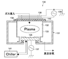
- FIG. 2 is a schematic configuration diagram of an etching apparatus for forming the magnetic layer pattern 12P.
- the illustrated etching apparatus 130 is configured as a magnetic field inductively coupled plasma etching apparatus, but is not limited to this.
- the etching apparatus 130 includes a chamber 131 that can be evacuated. Inside the chamber 131, a stage 135 for supporting the substrate is installed. An electrostatic chuck for holding the substrate placed on the stage 135 is provided on the upper surface of the stage 135, and a mechanism is provided for introducing heat to the back surface of the substrate after chucking so as to equalize the heat.
- the etching apparatus 130 includes a chiller circulation unit 141 that circulates the heat medium while controlling the temperature on the upper surface of the stage 135 or inside the stage 135. The chiller circulation unit 141 can maintain the stage 135 at a predetermined temperature.
- an adhesion preventing plate 133 that partitions the plasma forming space 132 is provided.
- the etching apparatus 130 forms a plasma of a reactive gas (etchant) introduced into the plasma forming space 132 and generates radicals of the reactive gas, thereby forming a magnetic layer on the substrate placed on the stage 135. 12 is etched.
- a reactive gas etchant
- a chlorine-based gas is used as the reactive gas.
- Cl 2 is used, but besides this, BCl 3 , SiCl 4, etc. can be applied.
- a mixed gas of a chlorine-based gas and an inert gas such as argon or nitrogen may be used as the etching gas. Chlorine radicals chemically etch the magnetic layer by chemically reacting with the magnetic layer to generate a chlorine compound of Co or Fe having a high vapor pressure.
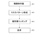
- FIG. 3 is a process flow illustrating a method for manufacturing the magnetic transfer master 10.
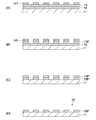
- FIG. 4 is a main process diagram thereof.
- the manufacturing method of the master 10 for magnetic transfer includes a laminate manufacturing process (step ST1, FIG. 4A), a mask pattern forming process (step ST2, FIG. 4B), and a magnetic layer.
- An etching process step ST3, FIG. 4C
- a cleaning process step ST4, FIG. 4D
- the stacked body 40 is manufactured by sequentially stacking the magnetic layer 12 and the mask layer 13 on the substrate 11.
- Each layer is formed in a predetermined thickness by a thin film forming method such as sputtering or CVD.
- the thickness of the magnetic layer 12 is 50 nm or more and 500 nm or less
- each thickness of the mask layer 13 is 10 nm or more and 100 nm or less.
- the mask layer 13 constitutes a metal layer that functions as an etching mask (mask pattern) for the magnetic layer 12.
- Ru ruthenium
- Cr chromium
- the resist mask 14P is formed on the mask layer 13, a resist mask 14P for patterning the mask layer 13 is formed.
- the resist mask 14P is formed by using a general photolithography technique, and description thereof is omitted here.
- the mask layer 13 is patterned.
- a dry etching apparatus having the same configuration as the etching apparatus shown in FIG. 2 is used.
- the substrate on which the stacked body 40 is formed is loaded into an etching chamber, and plasma of a mixed gas of chlorine and oxygen is formed, whereby the mask layer 13 is etched.
- a mask pattern 13P having a pattern shape corresponding to the resist mask 14P is formed.
- the etching conditions are as follows: the substrate temperature is room temperature, the gas pressure is 1 Pa, the chlorine (Cl 2 ) flow rate is 10 sccm, the oxygen (O 2 ) flow rate is 25 sccm, the antenna input power is 200 W, and the bias input power is 50 W (0.28 W / cm 2). ).
- the resist mask 14P is removed as shown in FIG. An ashing process using oxygen (O 2 ) or hydrogen (H 2 ) plasma is applied to remove the resist mask 14P.
- Magnetic layer etching process Next, as shown in FIG. 4C, etching for patterning the magnetic layer 12 is performed.
- the magnetic layer 12 is etched by chlorine-based gas plasma under a substrate temperature of 100 ° C. or higher. Thereby, the magnetic layer pattern 12P having a shape corresponding to the mask pattern 13P is formed.
- FIG. 5 shows one experimental result showing the relationship between the substrate temperature (° C.) and the etching rate (nm / min) of the magnetic layer 12.
- the measurement points were 20 ° C., 50 ° C., 100 ° C., 150 ° C., and 200 ° C.
- the experimental conditions were a pressure of 1.0 Pa, an antenna input power of 1500 W (13.56 MHz), and a bias input power of 0.17 W / cm 2 (12.5 MHz).
- the bias input power was a value obtained by dividing the input power by the area of the stage 135 (in this example, a diameter of 15 cm) (the same applies hereinafter).
- the etching rate of FeCo was 30 nm / min. Further, when the substrate temperature was 100 ° C. or higher, the FeCo etching rate increased as the temperature increased. When the substrate temperature was 200 ° C., an etching rate of 130 nm / min or higher was obtained. This is presumably because the chemical reaction between chlorine radicals and FeCo is promoted by heating the substrate.
- the upper limit of the substrate temperature is not particularly limited, but the upper limit can be appropriately determined according to the heat resistance of each layer including the magnetic layer 12. In the present embodiment, the etching temperature (substrate temperature) of the magnetic layer 12 is set to 150 ° C. or higher and 300 ° C.
- the etching pressure can be set in the range of 0.1 Pa to 5.0 Pa. Furthermore, the etching rate of the magnetic layer 12 can be controlled not only by the substrate temperature but also by the input power to the antenna 138 of the etching apparatus 130, the bias input power to the stage 135, and the like.
- the mask pattern 13P made of Ru or Cr is used for the etching mask of the magnetic layer 12, the heat resistance of the mask can be improved as compared with the photoresist mask made of an organic material. Therefore, it is possible to avoid the deterioration of the mask due to the heat treatment of the substrate during the etching process, and it is possible to etch the magnetic layer 12 with high accuracy.
- the mask pattern 13P is not etched only with a chlorine-based gas. Therefore, in the present embodiment in which chlorine alone gas is used for etching the magnetic layer 12, it is possible to etch the magnetic layer 12 with high accuracy by increasing the selectivity with the mask pattern 13P.
- the magnetic layer 12 can be etched while ensuring a good selection ratio with the mask pattern 13P.
- an appropriate etching process for the magnetic layer 12 can be stably realized by the above-described etching conditions.
- Pure water is used as the cleaning liquid, but ion-exchanged water, micro / nano bubble water, and various organic solvents can be used in addition to this.
- the organic solvent include ethanol, methanol, acetone, isopropyl alcohol, and ethyl ether.
- a cleaning method an immersion method in which the substrate is immersed in a cleaning liquid, a spray method, a spin coating method, or the like is applicable. After the cleaning process, a substrate drying process is performed.
- the above-described cleaning process can be omitted as necessary. Moreover, it may replace with the said washing
- dechlorination from the above-described chloride-based reaction product is possible, and thus the same effect as that obtained when the above washing step is performed can be obtained.
- low-density Fe-based or Co-based deposits may remain, but these deposits do not greatly affect the pattern accuracy of the magnetic layer pattern 12P as the magnetic transfer layer. It does not have to be removed.
- the substrate is dried. Thereafter, as shown in FIG. 4D, the master pattern 10 for magnetic transfer is manufactured by removing the mask pattern 13P.
- a method for removing the mask pattern 13P an etching process using plasma of a mixed gas of chlorine and oxygen can be employed.
- the etching gas is not limited to the above example, and a fluorine-based gas or a fluorocarbon-based gas may be used.
- a high selection ratio can be ensured between the magnetic layer 12 and the mask pattern 13P, so that the patterning of the magnetic layer 12 with excellent shape accuracy is possible. Become. Thereby, since the magnetic layer pattern 12P can be formed with high accuracy, it is possible to cope with the miniaturization of the magnetic layer pattern 12P.
- Ru and Cr constituting the mask pattern 13P are not etched only by the chlorine-based gas, but are etched by adding oxygen to the chlorine-based gas. In other words, etching progresses by generating RuO 4 in Ru and CrO 2 Cl 2 in Cr.
- a fluorine-based gas can be used as the etching gas for the mask pattern.
- the etching selectivity between FeCo and Cr and the etching selectivity between FeCo and Ru in the etching process of the magnetic layer 12 were measured, respectively.
- the measurement results are shown in FIG.
- the experimental conditions were a substrate temperature of 190 ° C., a gas pressure of 0.5 Pa, an etching gas of chlorine (Cl 2 ) gas, an antenna input power of 2000 W, and a bias input power of 150 W (0.85 W / cm 2 ).
- the etching rates of FeCo, Cr, and Ru were 40 nm / min, 3.1 nm / min, and 1 nm / min, respectively.
- the etching selectivity of FeCo to Cr was 12.9, and the etching selectivity of FeCo to Ru was 40. From the above results, it was confirmed that Cr and Ru can obtain a sufficient selection ratio as an FeCo etching mask.
- the magnetic layer 12 is etched mainly by a chemical reaction, it is possible to avoid reattachment to the mask side surface of the material to be etched, as compared with a physical etching method such as an ion milling method, A fine pattern can be stably formed. Further, since the etching gas for the magnetic layer 12 does not contain oxygen, oxidation of the FeCo layer during etching can be prevented, and desired magnetic characteristics required for the magnetic transfer layer can be ensured.
- FIG. 7 is a cross-sectional view showing a schematic configuration of a magnetic transfer master according to another embodiment of the present invention.
- an intermediate layer 15 is formed between the substrate 11 and the magnetic layer pattern 12P.
- the intermediate layer 15 can be made of a material having a function of improving the adhesion between the substrate 11 and the magnetic layer pattern 12P.
- a material having a function of protecting the substrate 11 from plasma when the magnetic layer pattern 12P is formed may be used.
- the master 20 for magnetic transfer shown in FIG. 7 is manufactured through a process similar to that described above after a laminated body in which the intermediate layer 15, the magnetic layer 12, and the mask layer 13 are sequentially formed on the substrate 11. be able to.
- the intermediate layer 15 by forming the intermediate layer 15 with a material having resistance to etching with respect to chlorine plasma, a function of protecting the substrate 11 from chlorine plasma during overetching of the magnetic layer 12 can be obtained.
- a material ruthenium, chromium, nickel and the like, alloys thereof, alloys containing these materials, and the like are applicable.
- the FeCo alloy is described as an example of the magnetic layer 12.
- the present invention is not limited to this, and other ferromagnetic materials such as a simple Fe, a simple Co, and a CoFeB alloy may be used. These materials can obtain a high etching rate similarly to the FeCo alloy.
- FIG. 8 is an experimental result showing the dependence of the etching rate on the antenna input power measured for FeCo, Fe, Co, and CoFeB as the magnetic layer.
- the experimental conditions at this time were an antenna frequency of 13.56 MHz, a pressure of 1.0 Pa, a substrate temperature of 190 ° C., and a bias input power of 0.17 W / cm 2 (12.5 MHz).
Landscapes
- Drying Of Semiconductors (AREA)
- Manufacturing Of Magnetic Record Carriers (AREA)
Abstract
【課題】磁性層パターンを高精度に形成することが可能な磁気転写用原盤の製造方法を提供する。 【解決手段】本発明の一実施形態に係る磁気転写用原盤の製造方法は、基板11上に、FeCo合金からなる磁性層12を磁気転写層として形成する工程と、磁性層12の上に、マスクパターン13Pを形成する工程と、上記基板を100℃以上の温度に保持し、塩素系ガスのプラズマを形成することで、磁性層12をマスクパターン13Pを介してエッチングする工程とを含む。これにより、磁気転写層のエッチング性が高まり、磁気転写層を精度よくパターニングすることが可能となる。
Description
本発明は、磁気記録媒体に対して情報を磁気転写するための磁気転写用原盤の製造方法に関する。
ハードディスクドライブ(HDD)に使用される磁気ディスクは、ドライブに組み込まれる前に、フォーマット情報やアドレス情報、サーボ情報等の各種磁気情報が書き込まれる。磁気情報は、磁気ヘッドを用いて書き込むことが一般的であるが、磁気ディスクの記録密度が向上するに伴い、書き込みに要する時間が増加している。そこで、磁気情報を磁気ディスクに対して一括的に書き込む磁気転写法が提案されている。磁気転写法では、磁気情報の記録パターンに従って磁性層が形成されたマスターディスク(原盤)が用いられる。磁気転写法は、マスターディスク(原盤)と被転写用ディスク(スレーブディスク)とを相互に密着させ、片面又は両面から電磁石や永久磁石などで生成した外部磁界を印加することで、磁性層に対向するスレーブディスク上の領域を一括的に磁化させる。
マスターディスクの製造方法として、種々の方法が提案されている。例えば下記特許文献1及び特許文献2には、転写する情報に対応した凹凸パターンが表面に形成された基板を作製し、この基板の表面に電鋳を施して金属盤を作製し、当該金属盤を基板表面から剥離する、磁気転写用マスター担体の製造方法が記載されている。
しかしながら、特許文献1及び特許文献2に記載の方法では、電鋳法により作製した金属盤を基板から剥離する工程を有するため、この剥離時の応力で金属盤が反ってしまうおそれがある。従って、これらの方法では、磁性層パターンを高精度に形成することが困難であり、磁気情報の転写精度の向上を図ることも非常に困難である。
以上のような事情に鑑み、本発明の目的は、磁性層パターンを高精度に形成することが可能な磁気転写用原盤の製造方法を提供することにある。
上記目的を達成するため、本発明の一形態に係る磁気転写用原盤の製造方法は、基板上に、鉄及びコバルトの少なくとも一方を含有する磁気転写層を形成する工程を含む。上記磁気転写層の上に、マスクパターンが形成される。上記磁気転写層は、上記基板を100℃以上の温度に保持し、塩素系ガスのプラズマを形成することで、上記マスクパターンを介してエッチングされる。
本発明の一実施形態に係る磁気転写用原盤の製造方法は、基板上に、鉄(Fe)及びコバルト(Co)の少なくとも一方を含有する磁気転写層を形成する工程を含む。上記磁気転写層の上に、マスクパターンが形成される。上記磁気転写層は、上記基板を100℃以上の温度に保持し、塩素系ガスのプラズマを形成することで、上記マスクパターンを介してエッチングされる。
上記磁気転写用原盤の製造方法においては、塩素系ガスのプラズマを用いた反応性イオンエッチング(RIE:Reactive Ion Etching)法によって、基板上の磁気転写層を化学的にエッチングする。このとき、基板温度を100℃以上とすることにより、磁気転写層のエッチング性が高まり、磁気転写層を精度よくパターニングすることが可能となる。
ここで、基板温度が100℃未満の場合、磁気転写層のエッチングレートが低いことで生産性を損なうおそれがある。一方、基板温度が高いほどエッチングレートが上昇する傾向にあるため、基板温度に特に上限はないが、磁気転写層を含む各層の耐熱性等に応じて適宜上限を定めることができる。
磁気転写層は、Fe、Fe系合金、Co、Co系合金、FeCo系合金等の金属単体または合金で構成することができ、これ以外にも、FeCo/Pd等の人工格子も適用可能である。
磁気転写層のエッチングガスとしては、Cl2、BCl3、SiCl4等の塩素系ガスが用いられる。プラズマの形成方法は特に限定されず、誘導結合プラズマ、容量結合プラズマ、有磁場誘導結合プラズマ、電子サイクロトロン共鳴プラズマ等が適用可能である。エッチング時における基板温度は、典型的には、加熱源を用いて調整することができる。
上記マスクパターンは、クロム(Cr)又はルテニウム(Ru)で構成することができる。上記マスクパターンを構成するRu及びCrは、塩素系ガスのみではエッチングされず、塩素系ガスに酸素を加えることでエッチングされる。すなわち、RuではRuO4を、CrではCrO2Cl2が生成されることで、エッチングが進行する。このようなガスを用いてRuやCrマスクを形成し、塩素系ガスのみで上記磁気転写層をエッチングすることにより、Ru又はCrとの十分な選択比が得られ、良好なエッチングパターンを形成することができる。上記マスクパターンのエッチングガスとして他に、フッ素系ガスを用いることも可能である。
上記磁気転写用原盤の製造方法は、上記磁気転写層の形成前に、上記基板上に、上記塩素系ガスのプラズマに対して耐エッチング性を有する中間層を形成する工程をさらに具備してもよい。これにより、磁気転写層のオーバーエッチング時において、プラズマによる基板への悪影響を回避することができる。また、上記中間層を基板と磁気転写層との間の密着層として機能させることも可能である。このような中間層を構成する材料として、例えば、Ru、Cr、Ni等が挙げられる。
上記磁気転写用原盤の製造方法は、上記磁気転写層をエッチングした後、上記磁気転写層を洗浄する工程をさらに具備してもよい。Fe及びCoの塩化物は水溶性であるため、エッチング後、基板を洗浄することで、磁気転写層の表面に形成されたエッチング反応生成物を除去することができる。洗浄液としては、純水、イオン交換水、マイクロナノバブル水、各種有機溶剤を用いることができる。有機溶剤としては、エタノール、メタノール、アセトン、イソプロピルアルコール、エチルエーテルなどが挙げられる。
以下、図面を参照しながら、本発明の実施形態を説明する。
図1は、本発明の一実施形態に係る磁気転写用原盤の概略構成を示す断面図である。本実施形態の磁気転写用原盤10は、基板11と、磁気転写層としての磁性層パターン12Pとの積層構造を有している。磁気転写用原盤10は、図示しないスレーブディスクと相互に密着されることで、磁性層パターン12Pに対向するスレーブディスク上の領域を磁化させる。
基板11は、平坦な円盤(ディスク)状基板で構成されている。基板11は、例えば、シリコン基板、ガラス基板、セラミックス基板等で構成されている。基板11の厚みは特に限定されず、反りや歪みのない適度な剛性が得られる範囲において、適宜設定することが可能である。
磁性層パターン12Pは、強磁性材料で構成されている。強磁性材料として、典型的には、Fe系材料、Co系材料、FeCo系材料等の軟磁気特性を有する強磁性材料が挙げられる。B、P、Si等の半金属元素が添加されてもよい。強磁性材料として、FeCo/Pd等の人工格子材料等も含まれる。本実施形態では、磁性層パターン12Pは、FeCo合金(原子量比:75%Fe-25%Co)が用いられている。
磁性層パターン12Pは、基板11上に成膜された磁性層を所定形状にエッチングすることで形成される。磁性層パターン12Pは、所定のフォーマット情報やアドレス情報、サーボ情報等の記録パターンに従って形成されている。本実施形態において、磁性層パターン12Pは、後述するドライエッチング装置を用いたドライエッチング法で形成される。
図2は、磁性層パターン12Pを形成するためのエッチング装置の概略構成図である。図示するエッチング装置130は、有磁場誘導結合プラズマエッチング装置として構成されているが、勿論これに限られない。
エッチング装置130は、真空排気可能なチャンバ131を備える。チャンバ131の内部には、基板を支持するステージ135が設置されている。ステージ135の上面には、ステージ135上に載置された基板を保持する静電チャックが具備されており、チャック後基板裏面にHeを導入して均熱を図る機構となっている。エッチング装置130は、ステージ135の上面又はステージ135の内部において熱媒体を温度管理しながら循環させるチラー循環ユニット141を備えている。チラー循環ユニット141は、ステージ135を所定温度に保持することが可能である。
ステージ135の周囲には、プラズマ形成空間132を区画する防着板133が設置されている。エッチング装置130は、プラズマ形成空間132に導入された反応性ガス(エッチャント)のプラズマを形成し、当該反応性ガスのラジカルを生成することにより、ステージ135上に載置された基板上の磁性層12をエッチングする。
本実施形態では、反応性ガスとして、塩素系ガスが用いられる。塩素系ガスとしては、Cl2が用いられるが、これ以外にも、BCl3、SiCl4等が適用可能である。また、エッチングガスとして、塩素系ガスと、アルゴンや窒素などの不活性ガスとの混合ガスが用いられてもよい。塩素ラジカルは、磁性層と化学反応し蒸気圧の高いCo又はFeの塩素化合物を生成することで、磁性層を選択的にエッチングする。
プラズマの発生機構として、エッチング装置130は、アンテナ138と、高周波電源139と、マグネットユニット140と、ガス導入ライン等を備える。アンテナ138は、プラズマ形成空間132の上部を閉塞する蓋体134の上部に配置されており、高周波電源139に接続されることで、プラズマ形成空間132に高周波誘導電場を形成する。マグネットユニット140は、蓋体134の上部に設置されており、プラズマ形成空間132に固定磁場を形成する。ガス導入系を介してプラズマ形成空間132へ導入された反応性ガスは、アンテナ138による誘導電場の作用とマグネットユニット140による固定磁場の作用とを受けてプラズマ化する。エッチング装置130は、プラズマ中のイオンをステージ135側へ引き付けるバイアス電源137を備えてもよい。バイアス電源137は、高周波電源で構成することができる。
次に、図1に示した磁気転写用原盤10の製造方法について説明する。図3は、磁気転写用原盤10の製造方法を説明する工程フローである。図4は、その主な工程図である。
本実施形態に係る磁気転写用原盤10の製造方法は、積層体の作製工程(ステップST1、図4(A))と、マスクパターン形成工程(ステップST2、図4(B))と、磁性層エッチング工程(ステップST3、図4(C))と、洗浄工程(ST4、図4(D))とを有する。
(積層体作製工程)
図4(A)に示すように、基板11上に、磁性層12、マスク層13を順に積層することで、積層体40が作製される。各層は、スパッタリング法、CVD法等の薄膜形成方法によって所定厚みにそれぞれ形成される。ここでは、磁性層12の厚みを50nm以上500nm以下、マスク層13の各厚みを10nm以上100nm以下とした。
図4(A)に示すように、基板11上に、磁性層12、マスク層13を順に積層することで、積層体40が作製される。各層は、スパッタリング法、CVD法等の薄膜形成方法によって所定厚みにそれぞれ形成される。ここでは、磁性層12の厚みを50nm以上500nm以下、マスク層13の各厚みを10nm以上100nm以下とした。
(マスクパターン形成工程)
本実施形態において、マスク層13は、磁性層12に対するエッチングマスク(マスクパターン)として機能する金属層を構成する。マスク層13の構成材料には、Ru(ルテニウム)又はCr(クロム)が用いられる。マスク層13の上には、マスク層13をパターニングするためのレジストマスク14Pが形成される。レジストマスク14Pは、一般的なフォトリソグラフィ技術を用いて形成され、ここではその説明は省略する。
本実施形態において、マスク層13は、磁性層12に対するエッチングマスク(マスクパターン)として機能する金属層を構成する。マスク層13の構成材料には、Ru(ルテニウム)又はCr(クロム)が用いられる。マスク層13の上には、マスク層13をパターニングするためのレジストマスク14Pが形成される。レジストマスク14Pは、一般的なフォトリソグラフィ技術を用いて形成され、ここではその説明は省略する。
次に、図4(B)に示すように、マスク層13がパターニングされる。マスク層13のパターニングには、例えば、図2に示したエッチング装置と同様な構成を有するドライエッチング装置が用いられる。積層体40が形成された基板をエッチングチャンバ内に装填し、塩素と酸素の混合ガスのプラズマを形成することで、マスク層13がエッチングされる。これにより、レジストマスク14Pに対応するパターン形状を有するマスクパターン13Pが形成される。エッチング条件は、基板温度を室温、ガス圧力を1Pa、塩素(Cl2)流量を10sccm、酸素(O2)流量を25sccm、アンテナ入力パワーを200W、バイアス入力パワーを50W(0.28W/cm2)とした。
マスクパターン13Pの形成後、図4(C)に示すように、レジストマスク14Pが除去される。レジストマスク14Pの除去には、酸素(O2)又は水素(H2)のプラズマを用いたアッシング処理が適用される。
(磁性層エッチング工程)
次に、図4(C)に示すように、磁性層12に対するパターニングのためのエッチングを実施する。本実施形態では、基板温度100℃以上の条件で、塩素系ガスのプラズマによって磁性層12がエッチングされる。これにより、マスクパターン13Pに対応する形状の磁性層パターン12Pが形成される。
次に、図4(C)に示すように、磁性層12に対するパターニングのためのエッチングを実施する。本実施形態では、基板温度100℃以上の条件で、塩素系ガスのプラズマによって磁性層12がエッチングされる。これにより、マスクパターン13Pに対応する形状の磁性層パターン12Pが形成される。
図5は、基板温度(℃)と磁性層12のエッチング速度(nm/min)との関係を示す一実験結果である。測定点は、20℃、50℃、100℃、150℃、200℃とした。実験条件は、圧力1.0Pa、アンテナ入力パワー1500W(13.56MHz)、バイアス入力パワー0.17W/cm2(12.5MHz)とした。ここで、バイアス入力パワーは、入力電力をステージ135の面積(本例では直径15cm)で除した値とした(以下同様)。
図5に示すように、基板温度が20℃及び50℃の場合、FeCoのエッチング速度は30nm/minであった。また、基板温度が100℃以上において、温度の上昇に伴って、FeCoのエッチング速度が増加し、基板温度が200℃のとき130nm/min以上のエッチング速度が得られた。これは、基板の加熱によって塩素ラジカルとFeCoとの化学反応が促進されるためであると考えられる。基板温度の上限は特に制限されないが、磁性層12を含む各層の耐熱性等に応じて適宜上限を定めることができる。本実施形態では、磁性層12のエッチング温度(基板温度)は、150℃以上300℃以下に設定される。また、エッチング圧力は、0.1Pa以上5.0Pa以下の範囲で設定することができる。さらに、磁性層12のエッチング速度は、基板温度だけでなく、エッチング装置130のアンテナ138への入力パワーやステージ135へのバイアス入力パワー等によっても制御することが可能である。
以上の結果から、基板温度を100℃以上に設定することで、FeCoのエッチング性が高まり、磁性層12を精度よくパターニングすることが可能となるとともに、生産性の向上を図ることが可能となる。
そして、本実施形態では、磁性層12のエッチングマスクにRu又はCrからなるマスクパターン13Pが用いられているため、有機材料からなるフォトレジストマスクに比べてマスクの耐熱性を高めることができる。したがって、エッチング処理時における基板の加熱処理に起因するマスクの劣化を回避でき、磁性層12を高精度にエッチングすることが可能となる。
また、マスクパターン13Pは、塩素系ガスのみではエッチングが進行しない。従って、磁性層12のエッチングに塩素単独ガスを用いる本実施形態においては、マスクパターン13Pとの選択比を高めて磁性層12を高精度にエッチングすることが可能である。
以上のように、本実施形態によれば、マスクパターン13Pとの良好な選択比を確保しつつ磁性層12をエッチングすることができる。また、上述したエッチング条件によって、磁性層12に対する適正なエッチング処理を安定して実現することができる。
(洗浄工程)
磁性層12のエッチング工程においては、FeCoと塩素との反応生成物(FeCl2、FeCl3、CoCl2など)が、エッチングパターン(磁性層パターン12P)の側壁部に残存する傾向がある。これは、パターンの側壁部に対してはバイアス入力によるイオンのスパッタ効果が得られにくいことによる。上記反応生成物は水溶性であることから、本実施形態では、エッチング加工された磁性層パターン12Pの洗浄工程を実施する。当該洗浄工程により、磁性層パターン12Pのパターン側壁部に付着した反応生成物を除去できるため、磁性層パターン12Pの加工精度を高めることができる。
磁性層12のエッチング工程においては、FeCoと塩素との反応生成物(FeCl2、FeCl3、CoCl2など)が、エッチングパターン(磁性層パターン12P)の側壁部に残存する傾向がある。これは、パターンの側壁部に対してはバイアス入力によるイオンのスパッタ効果が得られにくいことによる。上記反応生成物は水溶性であることから、本実施形態では、エッチング加工された磁性層パターン12Pの洗浄工程を実施する。当該洗浄工程により、磁性層パターン12Pのパターン側壁部に付着した反応生成物を除去できるため、磁性層パターン12Pの加工精度を高めることができる。
洗浄液には純水が用いられるが、これ以外にも、イオン交換水、マイクロナノバブル水、各種有機溶剤を用いることができる。有機溶剤としては、エタノール、メタノール、アセトン、イソプロピルアルコール、エチルエーテルなどが挙げられる。洗浄方法としては、洗浄液へ基板を浸漬する浸漬法、スプレー法、回転塗布法等が適用可能である。洗浄工程の後、基板の乾燥工程が実施される。
上述の洗浄工程は、必要に応じて省略することが可能である。また、上記洗浄工程に代えて、磁性層パターン12Pを水素プラズマで処理する工程が実施されてもよい。これにより、上述した塩化物系の反応生成物からの脱塩素化が可能となるので、上記洗浄工程を実施した場合と同様の効果を得ることができる。この場合、低密度のFe系又はCo系の付着物が残存する場合があるが、これらの付着物は、磁気転写層としての磁性層パターン12Pのパターン精度に大きな影響を与えることはないため、除去されなくてもよい。
洗浄工程の後、基板を乾燥させる。その後、図4(D)に示すように、マスクパターン13Pを除去することで、磁気転写用原盤10が作製される。マスクパターン13Pの除去方法としては、塩素と酸素の混合ガスのプラズマを利用したエッチング処理が採用可能である。エッチングガスは上記の例に限られず、フッ素系のガスや炭化フッ素系のガスが用いられてもよい。
本実施形態の磁気転写用原盤の製造方法によれば、磁性層12とマスクパターン13Pとの間に高い選択比を確保することができるので、形状精度に優れた磁性層12のパターニングが可能となる。これにより、磁性層パターン12Pを高精度に形成することができるため、磁性層パターン12Pの微細化にも対応することが可能となる。
すなわち、マスクパターン13Pを構成するRu及びCrは、塩素系ガスのみではエッチングされず、塩素系ガスに酸素を加えることでエッチングされる。すなわち、RuではRuO4を、CrではCrO2Cl2が生成されることで、エッチングが進行する。このようなガスを用いてRuやCrマスクを形成し、塩素系ガスのみで磁性層12をエッチングすることにより、Ru又はCrとの十分な選択比が得られ、良好なエッチングパターンを形成することができる。上記マスクパターンのエッチングガスとして他に、フッ素系ガスを用いることも可能である。
磁性層12のエッチング工程におけるFeCoとCrとの間のエッチング選択比と、FeCoとRuとの間のエッチング選択比とをそれぞれ測定した。その測定結果を図6に示す。実験条件は、基板温度を190℃、ガス圧力を0.5Pa、エッチングガスを塩素(Cl2)ガス、アンテナ入力パワーを2000W、バイアス入力パワー150W(0.85W/cm2)とした。図6に示すように、FeCo、Cr及びRuのエッチング速度は、それぞれ、40nm/min、3.1nm/min、1nm/minであった。また、Crに対するFeCoのエッチング選択比は12.9であり、Ruに対するFeCoのエッチング選択比は40であった。以上の結果から、Cr及びRuは、FeCoのエッチングマスクとして十分な選択比を得られることが確認された。
また、本実施形態によれば、化学反応を主体として磁性層12をエッチングするため、イオンミリング法等の物理的エッチング方法に比べて、被エッチング材料のマスク側面への再付着などを回避でき、微細パターンを安定して形成することが可能となる。また、磁性層12のエッチングガスは酸素を含まないため、エッチング中におけるFeCo層の酸化を防止して、磁気転写層として要求される所望の磁気的特性を確保することができる。
以上、本発明の実施形態について説明したが、勿論、本発明はこれに限定されることはなく、本発明の技術的思想に基づいて種々の変形が可能である。
例えば、以上の実施形態では、磁気転写用原盤として、図1に示した構成を例に挙げて説明したが、これに代えて、図7に示すような構成を採用することも可能である。図7は、本発明の他の実施形態に係る磁気転写用原盤の概略構成を示す断面図である。図示する磁気転写用原盤20は、基板11と磁性層パターン12Pとの間に、中間層15が形成されている。中間層15は、基板11と磁性層パターン12Pとの間の密着性を高める機能を有する材料とすることができる。磁性層パターン12Pの形成時に、基板11をプラズマから保護する機能を有するものを用いてもよい。
図7に示した磁気転写用原盤20は、基板11の上に、中間層15、磁性層12及びマスク層13を順に形成した積層体を作製した後、上述と同様な工程を経て、製造することができる。このとき、中間層15を塩素プラズマに対して耐エッチング性を有する材料で構成することで、磁性層12のオーバーエッチング時における塩素プラズマからの基板11の保護機能を得ることができる。このような材料として、ルテニウム、クロム、ニッケル等やこれらの合金もしくはこれらの材料を含む合金等が適用可能である。
また、以上の実施形態では、磁性層12としてFeCo合金を例に挙げて説明したが、これに限られず、Fe単体、Co単体、CoFeB合金などの他の強磁性材料を用いてもよい。これらの材料は、FeCo合金と同様に高いエッチング速度を得ることができる。図8は、磁性層としてFeCo、Fe、Co及びCoFeBについて測定した、エッチング速度のアンテナ入力パワー依存性を示す一実験結果である。このときの実験条件は、アンテナ周波数13.56MHz、圧力1.0Pa、基板温度190℃、バイアス入力パワー0.17W/cm2(12.5MHz)とした。
さらに以上の実施形態では、アンテナおよびバイアスの周波数は、干渉を避けるため相互に異なる周波数の高周波を用いたが、高周波に限らずマイクロ波など、他の周波数を用いても実施可能である。
10、20…磁気転写用原盤
11…基板
12…磁性層
12P…磁性層パターン
13…マスク層
13P…マスクパターン
15…中間層
40…積層体
130…エッチング装置
11…基板
12…磁性層
12P…磁性層パターン
13…マスク層
13P…マスクパターン
15…中間層
40…積層体
130…エッチング装置
Claims (7)
- 基板上に、鉄及びコバルトの少なくとも一方を含有する磁気転写層を形成し、
前記磁気転写層の上に、マスクパターンを形成し、
前記基板を100℃以上の温度に保持し、塩素系ガスのプラズマを形成することで、前記磁気転写層を前記マスクパターンを介してエッチングする
磁気転写用原盤の製造方法。 - 請求項1に記載の磁気転写用原盤の製造方法であって、
前記マスクパターンは、クロム又はルテニウムで形成される
磁気転写用原盤の製造方法。 - 請求項2に記載の磁気転写用原盤の製造方法であって、
前記マスクパターンは、塩素系ガスと酸素との混合ガスのプラズマを用いたエッチングにより形成される
磁気転写用原盤の製造方法。 - 請求項3に記載の磁気転写用原盤の製造方法であって、
前記磁気転写層は、FeCo系合金又はFeCo系人工格子である
磁気転写用原盤の製造方法。 - 請求項1に記載の磁気転写用原盤の製造方法であって、さらに、
前記磁気転写層の形成前に、前記基板上に、前記塩素系ガスのプラズマに対して耐エッチング性を有する中間層を形成する
磁気転写用原盤の製造方法。 - 請求項5に記載の磁気転写用原盤の製造方法であって、
前記中間層は、クロム層、ルテニウム層又はニッケル層である
磁気転写用原盤の製造方法。 - 請求項1に記載の磁気転写用原盤の製造方法であって、さらに、
前記磁気転写層をエッチングした後、前記磁気転写層を洗浄する
磁気転写用原盤の製造方法。
Priority Applications (1)
| Application Number | Priority Date | Filing Date | Title |
|---|---|---|---|
| JP2011537110A JPWO2011048746A1 (ja) | 2009-10-23 | 2010-09-15 | 磁気転写用原盤の製造方法 |
Applications Claiming Priority (2)
| Application Number | Priority Date | Filing Date | Title |
|---|---|---|---|
| JP2009244090 | 2009-10-23 | ||
| JP2009-244090 | 2009-10-23 |
Publications (1)
| Publication Number | Publication Date |
|---|---|
| WO2011048746A1 true WO2011048746A1 (ja) | 2011-04-28 |
Family
ID=43899991
Family Applications (1)
| Application Number | Title | Priority Date | Filing Date |
|---|---|---|---|
| PCT/JP2010/005618 Ceased WO2011048746A1 (ja) | 2009-10-23 | 2010-09-15 | 磁気転写用原盤の製造方法 |
Country Status (3)
| Country | Link |
|---|---|
| JP (1) | JPWO2011048746A1 (ja) |
| TW (1) | TW201120878A (ja) |
| WO (1) | WO2011048746A1 (ja) |
Cited By (1)
| Publication number | Priority date | Publication date | Assignee | Title |
|---|---|---|---|---|
| WO2013161769A1 (ja) * | 2012-04-26 | 2013-10-31 | 東京エレクトロン株式会社 | プラズマ処理方法及びプラズマ処理装置 |
Citations (6)
| Publication number | Priority date | Publication date | Assignee | Title |
|---|---|---|---|---|
| JPH08269748A (ja) * | 1995-03-31 | 1996-10-15 | Toshiba Corp | 磁性体薄膜の加工方法 |
| JPH0997419A (ja) * | 1995-07-24 | 1997-04-08 | Toshiba Corp | 磁気ディスク、磁気ディスクの製造方法、及び磁気記録装置 |
| JP2005228462A (ja) * | 2003-11-20 | 2005-08-25 | Matsushita Electric Ind Co Ltd | マスター情報担体とその製造方法、磁気記録媒体への記録方法及び磁気記録媒体の製造方法並びに磁気記録再生装置 |
| JP2007335001A (ja) * | 2006-06-15 | 2007-12-27 | Fujifilm Corp | 磁気転写方法、磁気転写装置、磁気記録媒体、磁気記録再生装置 |
| JP2008065944A (ja) * | 2006-09-08 | 2008-03-21 | Ulvac Japan Ltd | 磁性層パターンの形成方法、磁気抵抗素子の製造方法、及び磁気記憶媒体の製造方法 |
| JP2009245555A (ja) * | 2008-03-31 | 2009-10-22 | Fujifilm Corp | 磁気転写用マスター担体の製造方法、磁気転写用マスター担体、磁気転写方法、及び磁気記録媒体 |
Family Cites Families (1)
| Publication number | Priority date | Publication date | Assignee | Title |
|---|---|---|---|---|
| JP4510796B2 (ja) * | 2006-11-22 | 2010-07-28 | 株式会社アルバック | 磁気記憶媒体の製造方法 |
-
2010
- 2010-09-15 JP JP2011537110A patent/JPWO2011048746A1/ja active Pending
- 2010-09-15 WO PCT/JP2010/005618 patent/WO2011048746A1/ja not_active Ceased
- 2010-09-29 TW TW99133141A patent/TW201120878A/zh unknown
Patent Citations (6)
| Publication number | Priority date | Publication date | Assignee | Title |
|---|---|---|---|---|
| JPH08269748A (ja) * | 1995-03-31 | 1996-10-15 | Toshiba Corp | 磁性体薄膜の加工方法 |
| JPH0997419A (ja) * | 1995-07-24 | 1997-04-08 | Toshiba Corp | 磁気ディスク、磁気ディスクの製造方法、及び磁気記録装置 |
| JP2005228462A (ja) * | 2003-11-20 | 2005-08-25 | Matsushita Electric Ind Co Ltd | マスター情報担体とその製造方法、磁気記録媒体への記録方法及び磁気記録媒体の製造方法並びに磁気記録再生装置 |
| JP2007335001A (ja) * | 2006-06-15 | 2007-12-27 | Fujifilm Corp | 磁気転写方法、磁気転写装置、磁気記録媒体、磁気記録再生装置 |
| JP2008065944A (ja) * | 2006-09-08 | 2008-03-21 | Ulvac Japan Ltd | 磁性層パターンの形成方法、磁気抵抗素子の製造方法、及び磁気記憶媒体の製造方法 |
| JP2009245555A (ja) * | 2008-03-31 | 2009-10-22 | Fujifilm Corp | 磁気転写用マスター担体の製造方法、磁気転写用マスター担体、磁気転写方法、及び磁気記録媒体 |
Cited By (4)
| Publication number | Priority date | Publication date | Assignee | Title |
|---|---|---|---|---|
| WO2013161769A1 (ja) * | 2012-04-26 | 2013-10-31 | 東京エレクトロン株式会社 | プラズマ処理方法及びプラズマ処理装置 |
| JPWO2013161769A1 (ja) * | 2012-04-26 | 2015-12-24 | 東京エレクトロン株式会社 | プラズマ処理方法及びプラズマ処理装置 |
| US9660182B2 (en) | 2012-04-26 | 2017-05-23 | Tokyo Electron Limited | Plasma processing method and plasma processing apparatus |
| KR102056751B1 (ko) * | 2012-04-26 | 2019-12-17 | 도쿄엘렉트론가부시키가이샤 | 플라즈마 처리 방법 및 플라즈마 처리 장치 |
Also Published As
| Publication number | Publication date |
|---|---|
| JPWO2011048746A1 (ja) | 2013-03-07 |
| TW201120878A (en) | 2011-06-16 |
Similar Documents
| Publication | Publication Date | Title |
|---|---|---|
| JP5411281B2 (ja) | 磁気抵抗素子の製造方法 | |
| US20060222898A1 (en) | Magnetic recording medium and production method therefor | |
| TWI449036B (zh) | 針對圖案化碟片媒材之電漿離子植入製程期間的基材溫度控制方法 | |
| JP2001274144A (ja) | ドライエッチング方法、微細加工方法及びドライエッチング用マスク | |
| JP5814868B2 (ja) | 磁気記録媒体の製造方法 | |
| US8673162B2 (en) | Methods for substrate surface planarization during magnetic patterning by plasma immersion ion implantation | |
| JP2008065944A (ja) | 磁性層パターンの形成方法、磁気抵抗素子の製造方法、及び磁気記憶媒体の製造方法 | |
| CN105668546A (zh) | 一种制备纳米尺度的石墨烯结构的方法 | |
| CN102438841A (zh) | 用于图案化介质中的岛与沟槽的比值优化的工艺 | |
| JP5651616B2 (ja) | 磁気記録媒体、及びその製造方法 | |
| JP2005056547A (ja) | 磁性材を含む被加工体の加工方法及び磁気記録媒体の製造方法 | |
| US9224413B2 (en) | Magnetic recording medium and method of manufacturing the same | |
| JP2016032028A (ja) | プラズマ処理装置及びプラズマ処理方法 | |
| US20140120249A1 (en) | Magnetic recording medium manufacturing method and micropattern manufacturing method | |
| US10233538B2 (en) | Demagnetization of magnetic media by C doping for HDD patterned media application | |
| CN101483046A (zh) | 图案化介质型磁记录介质的制造方法 | |
| JP5105248B2 (ja) | 凹凸パターンの形成方法およびパターンドメディア型磁気記録媒体の製造方法 | |
| JPWO2011048746A1 (ja) | 磁気転写用原盤の製造方法 | |
| JP2001274143A (ja) | ドライエッチング方法、微細加工方法及びドライエッチング用マスク | |
| JP5681624B2 (ja) | 炭素膜の形成方法、磁気記録媒体の製造方法及び炭素膜の形成装置 | |
| JP2013145611A (ja) | 磁気記録媒体及びその製造方法 | |
| JP2014120591A (ja) | プラズマエッチング方法 | |
| JP2004269910A (ja) | 磁性材のドライエッチング方法、磁性材及び磁気記録媒体 | |
| WO2012090474A1 (ja) | 電極膜の加工方法、磁性膜の加工方法、磁性膜を有する積層体、および該積層体の製造方法 | |
| WO2009139477A1 (ja) | 磁気記録媒体の製造方法、磁気記録媒体及び磁気記録再生装置 |
Legal Events
| Date | Code | Title | Description |
|---|---|---|---|
| 121 | Ep: the epo has been informed by wipo that ep was designated in this application |
Ref document number: 10824601 Country of ref document: EP Kind code of ref document: A1 |
|
| WWE | Wipo information: entry into national phase |
Ref document number: 2011537110 Country of ref document: JP |
|
| 122 | Ep: pct application non-entry in european phase |
Ref document number: 10824601 Country of ref document: EP Kind code of ref document: A1 |