WO2011037119A1 - 液晶表示装置 - Google Patents
液晶表示装置 Download PDFInfo
- Publication number
- WO2011037119A1 WO2011037119A1 PCT/JP2010/066348 JP2010066348W WO2011037119A1 WO 2011037119 A1 WO2011037119 A1 WO 2011037119A1 JP 2010066348 W JP2010066348 W JP 2010066348W WO 2011037119 A1 WO2011037119 A1 WO 2011037119A1
- Authority
- WO
- WIPO (PCT)
- Prior art keywords
- liquid crystal
- film
- group
- rth
- crystal display
- Prior art date
- Legal status (The legal status is an assumption and is not a legal conclusion. Google has not performed a legal analysis and makes no representation as to the accuracy of the status listed.)
- Ceased
Links
Images


Classifications
-
- G—PHYSICS
- G02—OPTICS
- G02F—OPTICAL DEVICES OR ARRANGEMENTS FOR THE CONTROL OF LIGHT BY MODIFICATION OF THE OPTICAL PROPERTIES OF THE MEDIA OF THE ELEMENTS INVOLVED THEREIN; NON-LINEAR OPTICS; FREQUENCY-CHANGING OF LIGHT; OPTICAL LOGIC ELEMENTS; OPTICAL ANALOGUE/DIGITAL CONVERTERS
- G02F1/00—Devices or arrangements for the control of the intensity, colour, phase, polarisation or direction of light arriving from an independent light source, e.g. switching, gating or modulating; Non-linear optics
- G02F1/01—Devices or arrangements for the control of the intensity, colour, phase, polarisation or direction of light arriving from an independent light source, e.g. switching, gating or modulating; Non-linear optics for the control of the intensity, phase, polarisation or colour
- G02F1/13—Devices or arrangements for the control of the intensity, colour, phase, polarisation or direction of light arriving from an independent light source, e.g. switching, gating or modulating; Non-linear optics for the control of the intensity, phase, polarisation or colour based on liquid crystals, e.g. single liquid crystal display cells
- G02F1/137—Devices or arrangements for the control of the intensity, colour, phase, polarisation or direction of light arriving from an independent light source, e.g. switching, gating or modulating; Non-linear optics for the control of the intensity, phase, polarisation or colour based on liquid crystals, e.g. single liquid crystal display cells characterised by the electro-optical or magneto-optical effect, e.g. field-induced phase transition, orientation effect, guest-host interaction or dynamic scattering
-
- G—PHYSICS
- G02—OPTICS
- G02F—OPTICAL DEVICES OR ARRANGEMENTS FOR THE CONTROL OF LIGHT BY MODIFICATION OF THE OPTICAL PROPERTIES OF THE MEDIA OF THE ELEMENTS INVOLVED THEREIN; NON-LINEAR OPTICS; FREQUENCY-CHANGING OF LIGHT; OPTICAL LOGIC ELEMENTS; OPTICAL ANALOGUE/DIGITAL CONVERTERS
- G02F1/00—Devices or arrangements for the control of the intensity, colour, phase, polarisation or direction of light arriving from an independent light source, e.g. switching, gating or modulating; Non-linear optics
- G02F1/01—Devices or arrangements for the control of the intensity, colour, phase, polarisation or direction of light arriving from an independent light source, e.g. switching, gating or modulating; Non-linear optics for the control of the intensity, phase, polarisation or colour
- G02F1/13—Devices or arrangements for the control of the intensity, colour, phase, polarisation or direction of light arriving from an independent light source, e.g. switching, gating or modulating; Non-linear optics for the control of the intensity, phase, polarisation or colour based on liquid crystals, e.g. single liquid crystal display cells
- G02F1/133—Constructional arrangements; Operation of liquid crystal cells; Circuit arrangements
- G02F1/1333—Constructional arrangements; Manufacturing methods
- G02F1/1334—Constructional arrangements; Manufacturing methods based on polymer dispersed liquid crystals, e.g. microencapsulated liquid crystals
-
- G—PHYSICS
- G02—OPTICS
- G02B—OPTICAL ELEMENTS, SYSTEMS OR APPARATUS
- G02B5/00—Optical elements other than lenses
- G02B5/30—Polarising elements
- G02B5/3083—Birefringent or phase retarding elements
-
- G—PHYSICS
- G02—OPTICS
- G02F—OPTICAL DEVICES OR ARRANGEMENTS FOR THE CONTROL OF LIGHT BY MODIFICATION OF THE OPTICAL PROPERTIES OF THE MEDIA OF THE ELEMENTS INVOLVED THEREIN; NON-LINEAR OPTICS; FREQUENCY-CHANGING OF LIGHT; OPTICAL LOGIC ELEMENTS; OPTICAL ANALOGUE/DIGITAL CONVERTERS
- G02F1/00—Devices or arrangements for the control of the intensity, colour, phase, polarisation or direction of light arriving from an independent light source, e.g. switching, gating or modulating; Non-linear optics
- G02F1/01—Devices or arrangements for the control of the intensity, colour, phase, polarisation or direction of light arriving from an independent light source, e.g. switching, gating or modulating; Non-linear optics for the control of the intensity, phase, polarisation or colour
- G02F1/13—Devices or arrangements for the control of the intensity, colour, phase, polarisation or direction of light arriving from an independent light source, e.g. switching, gating or modulating; Non-linear optics for the control of the intensity, phase, polarisation or colour based on liquid crystals, e.g. single liquid crystal display cells
- G02F1/133—Constructional arrangements; Operation of liquid crystal cells; Circuit arrangements
- G02F1/1333—Constructional arrangements; Manufacturing methods
- G02F1/1335—Structural association of cells with optical devices, e.g. polarisers or reflectors
- G02F1/133528—Polarisers
-
- G—PHYSICS
- G02—OPTICS
- G02F—OPTICAL DEVICES OR ARRANGEMENTS FOR THE CONTROL OF LIGHT BY MODIFICATION OF THE OPTICAL PROPERTIES OF THE MEDIA OF THE ELEMENTS INVOLVED THEREIN; NON-LINEAR OPTICS; FREQUENCY-CHANGING OF LIGHT; OPTICAL LOGIC ELEMENTS; OPTICAL ANALOGUE/DIGITAL CONVERTERS
- G02F1/00—Devices or arrangements for the control of the intensity, colour, phase, polarisation or direction of light arriving from an independent light source, e.g. switching, gating or modulating; Non-linear optics
- G02F1/01—Devices or arrangements for the control of the intensity, colour, phase, polarisation or direction of light arriving from an independent light source, e.g. switching, gating or modulating; Non-linear optics for the control of the intensity, phase, polarisation or colour
- G02F1/13—Devices or arrangements for the control of the intensity, colour, phase, polarisation or direction of light arriving from an independent light source, e.g. switching, gating or modulating; Non-linear optics for the control of the intensity, phase, polarisation or colour based on liquid crystals, e.g. single liquid crystal display cells
- G02F1/133—Constructional arrangements; Operation of liquid crystal cells; Circuit arrangements
- G02F1/1333—Constructional arrangements; Manufacturing methods
- G02F1/1335—Structural association of cells with optical devices, e.g. polarisers or reflectors
- G02F1/13363—Birefringent elements, e.g. for optical compensation
-
- G—PHYSICS
- G02—OPTICS
- G02F—OPTICAL DEVICES OR ARRANGEMENTS FOR THE CONTROL OF LIGHT BY MODIFICATION OF THE OPTICAL PROPERTIES OF THE MEDIA OF THE ELEMENTS INVOLVED THEREIN; NON-LINEAR OPTICS; FREQUENCY-CHANGING OF LIGHT; OPTICAL LOGIC ELEMENTS; OPTICAL ANALOGUE/DIGITAL CONVERTERS
- G02F1/00—Devices or arrangements for the control of the intensity, colour, phase, polarisation or direction of light arriving from an independent light source, e.g. switching, gating or modulating; Non-linear optics
- G02F1/01—Devices or arrangements for the control of the intensity, colour, phase, polarisation or direction of light arriving from an independent light source, e.g. switching, gating or modulating; Non-linear optics for the control of the intensity, phase, polarisation or colour
- G02F1/13—Devices or arrangements for the control of the intensity, colour, phase, polarisation or direction of light arriving from an independent light source, e.g. switching, gating or modulating; Non-linear optics for the control of the intensity, phase, polarisation or colour based on liquid crystals, e.g. single liquid crystal display cells
- G02F1/133—Constructional arrangements; Operation of liquid crystal cells; Circuit arrangements
- G02F1/1333—Constructional arrangements; Manufacturing methods
- G02F1/1343—Electrodes
- G02F1/134309—Electrodes characterised by their geometrical arrangement
- G02F1/134363—Electrodes characterised by their geometrical arrangement for applying an electric field parallel to the substrate, i.e. in-plane switching [IPS]
-
- G—PHYSICS
- G02—OPTICS
- G02F—OPTICAL DEVICES OR ARRANGEMENTS FOR THE CONTROL OF LIGHT BY MODIFICATION OF THE OPTICAL PROPERTIES OF THE MEDIA OF THE ELEMENTS INVOLVED THEREIN; NON-LINEAR OPTICS; FREQUENCY-CHANGING OF LIGHT; OPTICAL LOGIC ELEMENTS; OPTICAL ANALOGUE/DIGITAL CONVERTERS
- G02F1/00—Devices or arrangements for the control of the intensity, colour, phase, polarisation or direction of light arriving from an independent light source, e.g. switching, gating or modulating; Non-linear optics
- G02F1/01—Devices or arrangements for the control of the intensity, colour, phase, polarisation or direction of light arriving from an independent light source, e.g. switching, gating or modulating; Non-linear optics for the control of the intensity, phase, polarisation or colour
- G02F1/13—Devices or arrangements for the control of the intensity, colour, phase, polarisation or direction of light arriving from an independent light source, e.g. switching, gating or modulating; Non-linear optics for the control of the intensity, phase, polarisation or colour based on liquid crystals, e.g. single liquid crystal display cells
- G02F1/137—Devices or arrangements for the control of the intensity, colour, phase, polarisation or direction of light arriving from an independent light source, e.g. switching, gating or modulating; Non-linear optics for the control of the intensity, phase, polarisation or colour based on liquid crystals, e.g. single liquid crystal display cells characterised by the electro-optical or magneto-optical effect, e.g. field-induced phase transition, orientation effect, guest-host interaction or dynamic scattering
- G02F1/13775—Polymer-stabilized liquid crystal layers
-
- G—PHYSICS
- G02—OPTICS
- G02F—OPTICAL DEVICES OR ARRANGEMENTS FOR THE CONTROL OF LIGHT BY MODIFICATION OF THE OPTICAL PROPERTIES OF THE MEDIA OF THE ELEMENTS INVOLVED THEREIN; NON-LINEAR OPTICS; FREQUENCY-CHANGING OF LIGHT; OPTICAL LOGIC ELEMENTS; OPTICAL ANALOGUE/DIGITAL CONVERTERS
- G02F1/00—Devices or arrangements for the control of the intensity, colour, phase, polarisation or direction of light arriving from an independent light source, e.g. switching, gating or modulating; Non-linear optics
- G02F1/01—Devices or arrangements for the control of the intensity, colour, phase, polarisation or direction of light arriving from an independent light source, e.g. switching, gating or modulating; Non-linear optics for the control of the intensity, phase, polarisation or colour
- G02F1/13—Devices or arrangements for the control of the intensity, colour, phase, polarisation or direction of light arriving from an independent light source, e.g. switching, gating or modulating; Non-linear optics for the control of the intensity, phase, polarisation or colour based on liquid crystals, e.g. single liquid crystal display cells
- G02F1/137—Devices or arrangements for the control of the intensity, colour, phase, polarisation or direction of light arriving from an independent light source, e.g. switching, gating or modulating; Non-linear optics for the control of the intensity, phase, polarisation or colour based on liquid crystals, e.g. single liquid crystal display cells characterised by the electro-optical or magneto-optical effect, e.g. field-induced phase transition, orientation effect, guest-host interaction or dynamic scattering
- G02F1/13793—Blue phases
-
- G—PHYSICS
- G02—OPTICS
- G02F—OPTICAL DEVICES OR ARRANGEMENTS FOR THE CONTROL OF LIGHT BY MODIFICATION OF THE OPTICAL PROPERTIES OF THE MEDIA OF THE ELEMENTS INVOLVED THEREIN; NON-LINEAR OPTICS; FREQUENCY-CHANGING OF LIGHT; OPTICAL LOGIC ELEMENTS; OPTICAL ANALOGUE/DIGITAL CONVERTERS
- G02F2413/00—Indexing scheme related to G02F1/13363, i.e. to birefringent elements, e.g. for optical compensation, characterised by the number, position, orientation or value of the compensation plates
Definitions
- the present invention relates to improvement of display characteristics of a liquid crystal display device using a polymer-stabilized blue phase.
- Liquid crystal display elements are widely used in the field of optical information processing.
- liquid crystal display methods such as TN, STN, IPS, VA, and OCB methods
- the alignment of liquid crystal molecules that is controlled in advance between two polarizing plates varies depending on the applied electric field.
- display is performed by changing the state of light, changing the polarization direction or polarization state of light, and changing the amount of transmitted light.
- All of these conventional liquid crystal display systems require a surface alignment process for controlling the alignment of liquid crystal molecules, and in particular, a system other than VA requires a rubbing process.
- the rubbing is an operation of rubbing the surface of the alignment film applied to the substrate surface in contact with the liquid crystal with a cloth or the like, which causes a decrease in yield, an increase in cost due to the decrease, and a decrease in display quality.
- the response time is about 5 milliseconds at the shortest, and there is a limit to the display of moving images on a television.
- Patent Documents 1 and 2 chiral nematic liquid crystals have been developed as liquid crystals for liquid crystal display elements.
- use of a polymer-stabilized blue phase has been proposed in place of conventional nematic liquid crystals (Patent Documents 3 and 4).
- This polymer-stabilized blue phase is a novel material whose expression temperature range is significantly increased by a polymer without losing the high-speed response characteristic of the blue phase. Since the polymer-stabilized blue phase is optically isotropic when no electric field is applied, it is not necessary to control the orientation. Display is performed by a novel method that utilizes a phenomenon in which retardation is induced by application of an electric field without retardation at zero electric field.
- the present inventors have the above advantages, but the front (normal direction to the display surface) CR is lower than other liquid crystal display methods. I found out that there was a problem. In recent years, since the liquid crystal display device has been improved in CR, it is strongly desired to improve the front CR of the liquid crystal display device using the polymer-stabilized blue phase.
- the present invention has been made in view of the above problems, and an object thereof is to improve the front CR of a liquid crystal display device using a polymer-stabilized blue phase.
- the present inventors diligently studied.
- One of the causes of the low front CR of the liquid crystal display device using the polymer-stabilized blue phase is that the blue phase is stabilized for the blue phase.
- the reaction did not proceed sufficiently.
- the color filter substrate and the array substrate of the liquid crystal cell hinder the transmission of ultraviolet rays, the entire surface or part of the liquid crystal cell is not uniformly irradiated with ultraviolet rays, and the progress of the photocrosslinking reaction is hindered. all right.
- a liquid crystal cell having a light source, a first polarizer, a first transparent film, a pair of transparent substrates and a polymer-stabilized blue phase liquid crystal disposed therebetween, a second transparent film, and a second A liquid crystal display device, wherein polarizers are arranged in this order, one of a pair of transparent substrates is an array substrate, and a color filter layer is not arranged on the other transparent substrate.
- the array substrate is a color filter-on-array substrate.
- the liquid crystal display device according to [1] or [2], which includes a backlight unit that sequentially emits independent three primary color lights and is driven by a field sequential driving method.
- of the in-plane retardation Re (550) at a wavelength of 550 nm of the first transparent film is 20 nm or less and the thickness direction retardation Rth (550) of the same wavelength is less than 20 nm.
- of the in-plane retardation Re (550) at a wavelength of 550 nm of the first transparent film is 10 nm or less and the thickness direction retardation Rth (550) of the same wavelength is [4]
- the liquid crystal display device having an absolute value
- of the first transparent film is 10 nm or less and
- the second transparent film is a biaxial film having Re (550) of 200 to 350 nm and Rth (550) of ⁇ 88 to 88 nm.
- Liquid crystal display device [16]
- the second transparent film is a biaxial film in which Re (550) is 20 to 120 nm and Rth (550) is 125 to 225 nm, and Re (550) is ⁇ 30 to 30 nm.
- the liquid crystal display device according to any one of [1] to [11], further including a biaxial film having Rth (550) of 50 to 150 nm.
- the second transparent film has a Re (550) of 60 to 210 nm and a Rth (550) of 30 to 105 nm, and Re (550) of ⁇ 30 to 30 nm.
- the present invention by using a polymer-stabilized blue phase, it is possible to provide a liquid crystal display device having a high response speed and an improved front CR.
- FIG. 1 is a schematic cross-sectional view of an example of a COA substrate that can be used in the present invention. It is a cross-sectional schematic diagram of an example of the counter substrate of the COA substrate that can be used in the present invention. It is sectional drawing which shows an example of the liquid crystal display element which can be utilized for this invention. It is sectional drawing which shows an example of the liquid crystal display element which can be utilized for this invention. It is a top view which shows the structural example of the electrode of the liquid crystal display element which can be utilized for this invention.
- (A) is sectional drawing which shows typically the schematic structure of the principal part of the said display element in an electric field no application state
- (b) shows typically the schematic structure of the principal part of the said display element in an electric field application state.
- It is a sectional view It is a block diagram which shows schematic structure of the principal part of an example of the display apparatus of this invention. It is a top view which shows the structural example of the electrode of the liquid crystal display element which can be utilized for this invention.
- Re ( ⁇ ) and Rth ( ⁇ ) represent in-plane retardation (unit: nm) and retardation in the thickness direction (unit: nm) at wavelength ⁇ , respectively.
- Re ( ⁇ ) is measured by making light with a wavelength of ⁇ nm incident in the normal direction of the film in KOBRA 21ADH or WR (manufactured by Oji Scientific Instruments).
- Rth ( ⁇ ) is calculated by the following method.
- Rth ( ⁇ ) is Re ( ⁇ )
- the in-plane slow axis (determined by KOBRA 21ADH or WR) is the tilt axis (rotation axis) (if there is no slow axis, any in-plane film surface)
- the light of wavelength ⁇ nm is incident from each of the inclined directions in steps of 10 degrees from the normal direction to 50 degrees on one side with respect to the film normal direction (with the direction of the rotation axis as the rotation axis).
- KOBRA 21ADH or WR is calculated based on the measured retardation value, the assumed value of the average refractive index, and the input film thickness value.
- Re ( ⁇ ) represents a retardation value in a direction inclined by an angle ⁇ from the normal direction.
- nx represents the refractive index in the slow axis direction in the plane
- ny represents the refractive index in the direction orthogonal to nx in the plane
- nz represents the refractive index in the direction orthogonal to nx and ny.
- d represents the film thickness of the film.
- Rth ( ⁇ ) is calculated by the following method.
- Rth ( ⁇ ) is from ⁇ 50 degrees to +50 degrees with respect to the normal direction of the film, with Re ( ⁇ ) being the in-plane slow axis (determined by KOBRA 21ADH or WR) and the tilt axis (rotating axis).
- Re ( ⁇ ) being the in-plane slow axis (determined by KOBRA 21ADH or WR) and the tilt axis (rotating axis).
- ⁇ nm is incident from the inclined direction and measured at 11 points. Based on the measured retardation value, the assumed average refractive index, and the input film thickness value, KOBRA 21ADH or Calculated by WR.
- the assumed value of the average refractive index the values of Polymer Handbook (John Wiley & Sons, Inc.) and catalogs of various optical films can be used. Those whose average refractive index is not known can be measured with an Abbe refractometer. Examples of the average refractive index values of main optical films are given below: Cellulose acylate (1.48), cycloolefin polymer (1.52), polycarbonate (1.59), polymethyl methacrylate (1.49), and polystyrene (1.59). The KOBRA 21ADH or WR calculates nx, ny, and nz by inputting the assumed value of the average refractive index and the film thickness.
- Nz (nx ⁇ nz) / (nx ⁇ ny) is further calculated from the calculated nx, ny, and nz.
- the measurement wavelength is 550 nm.
- the “in-plane slow axis” is the direction in which the refractive index is maximized in the plane, and the “in-plane slow axis” is the direction orthogonal to the in-plane slow axis in the plane.
- the visible light region means a wavelength of 380 to 780 nm.
- the present invention relates to a liquid crystal display device using a polymer-stabilized blue phase, and in particular, a high-level display in which an array substrate is disposed on one of a pair of substrates of a liquid crystal cell and a counter substrate without a color filter layer is disposed on the other.
- the present invention relates to a liquid crystal display device using a molecule-stabilized blue phase. It is known that a liquid crystal display device using a polymer-stabilized blue phase does not need to control orientation, has a high response speed, and exhibits a wide viewing angle characteristic. However, as a result of examination by the present inventors, it was found that the front CR is inferior to other liquid crystal display methods. One of the causes is an alignment defect in the liquid crystal layer.
- the polymer-stabilized blue phase has a structure in which the blue phase liquid crystal is stabilized by a polymer network, and therefore the liquid crystal alignment tends to be non-uniform and alignment defects are likely to occur.
- the front (normal direction with respect to the display surface) CR decreases due to the scattering phenomenon by the liquid crystal at the alignment defect portion. This orientation defect is more likely to occur as the polymer network is insufficiently formed.
- the color filter substrate and the array substrate of the liquid crystal cell impede the transmission of ultraviolet rays. Therefore, the entire surface or part of the liquid crystal cell is not uniformly irradiated with ultraviolet rays, and the photocrosslinking reaction occurs. It turned out that the progress was hindered. As a result, the reaction does not proceed sufficiently and the formation of the polymer network becomes insufficient, which contributes to the generation of orientation defects. Conventionally, since an array substrate is disposed on one of a pair of substrates of a liquid crystal cell and a color filter substrate is disposed on the other, the photo-crosslinking reaction or the like becomes insufficient even when irradiated with ultraviolet rays from either side.
- an array substrate is disposed on one of a pair of substrates of a liquid crystal cell, and a counter substrate having no color filter layer is disposed on the other. Therefore, when ultraviolet rays are irradiated from the counter substrate side, the light is transmitted by the color filter.
- the blue phase liquid crystal can be uniformly irradiated with ultraviolet rays without disturbing the above.
- the photocrosslinking reaction can proceed stably and sufficiently, and a polymer network for stabilizing the blue phase can be stably formed. If the blue phase is further stabilized by the polymer network, alignment defects are less likely to occur, and as a result, the reduction in front CR due to light scattering by the liquid crystal in the alignment defect portion can be reduced.
- the influence of the state of the polymer network of the polymer-stabilized blue phase on the front CR has not been studied at all, and is the first finding of the present inventors.
- One embodiment of the present invention is a liquid crystal display device having a COA structure in which a COA substrate is disposed on one of a pair of substrates of a liquid crystal cell, and a counter substrate having no color filter layer is disposed on the other.
- a COA substrate is disposed on one of a pair of substrates of a liquid crystal cell
- a counter substrate having no color filter layer is disposed on the other.
- the COA structure has been conventionally proposed as a structure capable of expanding the aperture ratio, but it is not yet known that it can be applied to a polymer-stabilized blue phase liquid crystal cell.
- an increase in the aperture ratio due to the adoption of the COA structure leads to an improvement in the transmittance during white display, while the front CR has two transmittances during white display and black display. Since it is determined by (white luminance and black luminance), increasing the aperture ratio by adopting the COA structure does not directly improve the front CR.
- another embodiment of the present invention is a liquid crystal cell having no color filter and a liquid crystal display device having no color filter and having a field sequential drive liquid crystal cell.
- the field sequential driving method even if there is no color filter layer, full color display is possible, for example, by using a backlight unit that sequentially emits independent three primary color (RGB) lights.
- RGB three primary color
- the blue phase liquid crystal is not disturbed by the color filter or the array if the ultraviolet light is irradiated from the counter substrate side. Can be irradiated with ultraviolet rays uniformly.
- the photocrosslinking reaction can proceed stably and sufficiently, and a polymer network for stabilizing the blue phase can be stably formed. If the blue phase is further stabilized by the polymer network, alignment defects are less likely to occur, and as a result, the reduction in front CR due to light scattering by the liquid crystal in the alignment defect portion can be reduced.
- the polymer-stabilized blue phase is isotropic when displaying black
- linearly polarized light that passes through the polarizer on the rear side (the light source side with respect to the blue phase liquid crystal) and proceeds in the normal direction is Even if it passes through the liquid crystal layer, its polarization state does not change, and in principle, it is absorbed by the absorption axis of the polarizer on the front side (observer side with respect to the blue phase liquid crystal). That is, in principle, it can be said that there is no light leakage in the normal direction during black display.
- the front transmittance during black display is not zero.
- the transmittance at the time of black display includes not only the fluctuation of the liquid crystal molecules in the liquid crystal layer but also the phase difference of the member disposed between the polarizer on the light source side and the liquid crystal cell. Also found that there is a cause.
- a light source side polarizer Normally, light having directivity is incident on a light source side polarizer from a backlight unit of a liquid crystal display device, but light incident from an oblique direction is a letter of a member that passes until it enters a liquid crystal cell. It is elliptically polarized by the foundation. After that, the elliptically polarized light is incident on the liquid crystal cell, and the present inventors diligently studied to find that the elliptically polarized light is converted into each member (liquid crystal, color filter, black matrix) in the liquid crystal cell.
- the light When the light is incident on the array substrate structure, the protrusion structure of the counter substrate, the slit on the common electrode on the counter substrate, etc., the light is scattered in the front due to optical phenomena such as scattering and diffraction in each member. Was found to be reduced. If the retardation of the member through which the linearly polarized light passes after passing through the polarizer and before entering the liquid crystal cell is low, the transmittance at the time of black display is increased by the optical phenomenon in each member arranged in the liquid crystal cell. Can be suppressed. Therefore, in the present invention, the lower the retardation of the transparent film disposed between the light source side polarizer and the liquid crystal layer, the better.
- the transparent film disposed between the light source side polarizer and the liquid crystal layer has
- the retardation of the transparent film disposed between the polarizer on the light source side and the liquid crystal layer also affects the so-called blackness change (color shift) with a tint that occurs in an oblique direction during black display.
- the transparent film disposed between the light source side polarizer and the liquid crystal layer has
- the transmittance ratio between the front white display and the black display (a high value can be achieved for the front CR, which is (brightness ratio), and the amount of change in blackness can be suppressed by suppressing light leakage during black display in a wide visible light wavelength range in an oblique direction.
- the liquid crystal display device of the present invention is suitable for the enlargement and quality improvement of the liquid crystal screen corresponding to the same plane switching method.
- the liquid crystal display device of the present invention uses a polymer-stabilized blue phase liquid crystal, it has the following advantages.
- the surface alignment treatment for controlling the alignment of the liquid crystal material is not required, and the alignment film is applied to the substrate surface, which is indispensable for the conventional display element-drying-alignment treatment such as thermal curing-rubbing-cleaning-drying, etc. All processes can be omitted. This process caused the entry of foreign matter such as dust and fine particles, the generation of static electricity, and the occurrence of scratches, which caused the yield and display function to be reduced. And degradation of the display function can be avoided.
- liquid crystal display elements have a fundamentally limited response time due to the change in the alignment state of nematic liquid crystal, which is inferior to the moving image display function compared to competing technologies such as plasma panels and EL.
- this problem can be solved because a response of about 100 ⁇ sec is possible.
- Examples of the polymer-stabilized blue phase liquid crystal material that can be used in the present invention include a low-molecular liquid crystal capable of developing a blue phase between a cholesteric phase and an isotropic phase, and a polymer formed in the low-molecular liquid crystal And a composite liquid crystal composition having a network.
- the polymer network is a polymer network formed by polymerizing a non-liquid crystalline or liquid crystalline monomer together with a crosslinking agent.
- the polymer-stabilized blue phase liquid crystal material preferably contains a chiral dopant. The amount of chiral dopant for the polymer-stabilized blue phase liquid crystal affects the diffraction wavelength of the polymer-stabilized blue phase liquid crystal.
- the addition amount of the chiral dopant may be adjusted so that the diffraction wavelength of the polymer-stabilized blue phase liquid crystal is outside the visible region (380 to 750 nm).
- the liquid crystal display device using the polymer-stabilized blue phase liquid crystal material containing such an added amount of chiral dopant further reduces light leakage during black display.
- the monomer used to form the polymer network may be either a non-liquid crystalline monomer or a liquid crystalline monomer, but the non-liquid crystalline monomer is more effective than the liquid crystalline monomer.
- a non-liquid crystalline monomer is a monomer that can be polymerized by photopolymerization or thermal polymerization, and has a rod-like molecular structure (for example, an alkyl group, a cyano group, or fluorine at the end of a biphenyl group or a biphenyl cyclohexyl group).
- a monomer having no molecular structure for example, a monomer containing a polymerizable group such as an acryloyl group, a methacryloyl group, a vinyl group, an epoxy group, a fumarate group, or a cinnamoyl group in the molecular structure.
- a monomer containing a polymerizable group such as an acryloyl group, a methacryloyl group, a vinyl group, an epoxy group, a fumarate group, or a cinnamoyl group in the molecular structure.
- a liquid crystal that has a rod-like or plate-like skeleton containing a phenyl group or a cyclohexyl group as a monomer other than a non-liquid crystalline monomer and exhibits liquid crystallinity by itself or a liquid crystal phase when mixed with other molecules Ionic monomer.
- a monomer having a plurality of polymerization groups may be used.
- non-liquid crystalline monomers include acrylate monomers having an acryloyl group or methacryloyl group in the molecular structure, and particularly preferable examples include branched acrylate monomers having an alkyl group as a side chain.
- the alkyl group is generally an alkyl group having 1 to 4 carbon atoms, and a monomer having at least one side chain composed of such an alkyl group per monomer unit is used.
- Preferred examples of the acrylate monomer include cyclohexyl acrylate, and preferred examples of the acrylate monomer having an alkyl group as a side chain include 2-ethylhexyl acrylate and 1,3,3-trimethylhexyl acrylate. Can do.
- This monomer is subjected to polymerization together with a crosslinking agent to form a polymer network.
- This cross-linking agent may be either a liquid crystalline or non-liquid crystalline compound, and a cross-linking agent having a reactive site that can form a network structure by bonding the monomer molecules corresponding to the monomer used is used. That's fine.
- a liquid crystalline diacrylate monomer can be used as a crosslinking agent.
- the low molecular liquid crystal constituting the polymer-stabilized blue phase liquid crystal material is a low molecular liquid crystal capable of expressing a blue phase between a cholesteric phase (chiral nematic phase) and an isotropic phase, preferably, It is a thermotropic liquid crystal composed of elongated rod-like molecules, and can be selected from various liquid crystal materials developed for liquid crystal display elements.
- low-molecular liquid crystals examples include molecular structures such as biphenyl, terphenyl, biphenyl cyclohexyl, etc., and themselves have chirality (chirality) due to the presence of asymmetric atoms, or chiral substances
- a (chiral dopant) a substance capable of developing a cholesteric phase (chiral nematic phase), in which the helical pitch length in the cholesteric phase (chiral nematic phase) is about 500 nm or less
- the chiral dopant causes a twisted structure in the liquid crystal.
- ZLI-4572 used in Examples described later, CB15 shown below, and furo [3, 2 shown as (a) to (h) below.
- -B] Derivatives having a furan structure.
- the chiral dopant is used as an additive to stabilize the twisted structure of the TN mode or induce a helical phase such as a cholesteric phase or a chiral smectic phase.
- a pitch length shorter than a normal pitch is preferable, it is preferable to add a material having a large helical twisting power (HTP) at a high concentration. Therefore, a chiral dopant having a large HTP and high solubility in liquid crystals is preferable.
- HTP helical twisting power
- the blue phase of the polymer-stabilized blue phase liquid crystal is obtained by dispersing a monomer and a crosslinking agent in a low molecular liquid crystal and performing a polymerization reaction at a temperature at which the blue phase is maintained.
- Polymerization can be performed by either thermal polymerization or photopolymerization.
- thermal polymerization there is a limit to the range in which the temperature at which the blue phase is maintained and the polymerization temperature (heating temperature) overlap, and the polymer Since the form of the network may change due to heating, it is preferable to use photopolymerization using ultraviolet light.
- the polymerization initiator it is preferable to disperse the polymerization initiator in addition to the monomer, the chiral dopant, and the crosslinking agent in the low-molecular liquid crystal in order to increase the polymerization rate.
- various initiators such as acetophenone, benzophenone, benzoin ether, and thioxanthone can be used, and specific examples include 2,2-dimethoxy-2-phenylacetophenone. .
- Adjustment of the amount of chiral dopant for the polymer-stabilized blue phase liquid crystal so that the diffraction wavelength of the polymer-stabilized blue phase liquid crystal is outside the visible region can be performed, for example, by the following procedure.
- a polymer-stabilized blue phase liquid crystal to which an appropriate amount of chiral dopant is added is prepared.
- the diffraction wavelength of this liquid crystal surface is measured according to a conventional method using a diffraction grating spectrometer (for example, a microscopic ultraviolet visible photometer 350 manufactured by JASCO Corporation).
- the amount of chiral dopant whose diffraction wavelength is outside the visible region is determined.
- the amount of the chiral dopant thus measured depends on the chiral dopant HTP (Helical Twisting Power) and differs depending on the kind of the chiral dopant and the liquid crystal.
- HTP Helical Twisting Power
- the amount of ZLI-4572 is about 6 to 10 mol%
- the amount of CB15 is about 85 to 95 mol. %.
- FIG. 1 shows a schematic diagram of an example of the liquid crystal display device of the present invention.
- the liquid crystal display device shown in FIG. 1 has a structure in which a polymer stable blue phase liquid crystal display element LC is sandwiched between two polarizing plates PL1 and PL2.
- the polarizing plate PL1 has a configuration in which the polarizing film 10 is sandwiched between two transparent films 14 and 18, and the polarizing plate PL2 has a configuration in which the polarizing film 12 is sandwiched between two transparent films 16 and 20. ing.
- the transparent films 14 and 16 on the polymer stable blue phase liquid crystal display element LC side affect the display performance, but the transparent film on the opposite side of the polymer stable blue phase liquid crystal display element 18 and 20 function as protective films for the polarizing films 10 and 12 and will not normally affect the display performance.
- a COA substrate 24 is disposed on one of a pair of substrates of a liquid crystal cell, and a counter substrate without a color filter layer is disposed on the other.
- of the transparent film 16 on the light source side is 20 nm or less, and
- the retardation of the transparent film 16 and preferably by controlling the wavelength dependence of Re and Rth, light leakage in the front direction during black display can be further reduced, and CR can be further improved. It is possible to reduce the tinting that occurs in the oblique direction. More specifically, the absolute value
- the transparent film 16 has a small wavelength dependency of Re and Rth, that is, it is preferable that the absolute values of Re and Rth satisfy the above conditions over the visible light region.
- the preferable wavelength dependence of Re and Rth is specifically that
- Re (400) of the transparent film 16 is preferably ⁇ 5 to 5 nm, and Rth (400) is more preferably ⁇ 10 to 10 nm.
- Re (700) of the transparent film 16 is preferably ⁇ 10 to 10 nm, and Rth (700) is more preferably ⁇ 10 to 10 nm.
- Display characteristics can be further improved by controlling the optical characteristics of the transparent film 14 disposed on the display surface side.
- a preferred example is an example in which the transparent film 14 also satisfies the optical characteristics required for the transparent film 16.
- Another preferred example is an example in which the transparent film 14 exhibits optical biaxiality.
- Re of the transparent film 14 is about 200 to 350 nm and Rth is about ⁇ 88 to 88 nm, more preferably, Re is about 250 to 300 nm and Rth is about ⁇ 45 to 45 nm.
- the transparent film 14 has a two-layer structure that optically exhibits biaxiality.
- one of the two sheets has a Re of the transparent film 14 of about 20 to 120 nm and an Rth of about 125 to 225 nm, more preferably an Re of about 40 to 100 nm and an Rth of about 145 to 205 nm.
- Re of the transparent film 14 is about ⁇ 30 to 30 nm and Rth is about 50 to 150 nm, more preferably, Re is about ⁇ 10 to 10 nm and Rth is about 80 to 120 nm.
- Another preferable example is an example in which the transparent film 14 is optically uniaxial.
- one of the two sheets has Re of the transparent film 14 of about 60 to 210 nm and Rth of about 30 to 105 nm, more preferably Re of about 110 to 160 nm and Rth of about 55 to 80 nm.
- Re of the transparent film 14 is about ⁇ 30 to 30 nm and Rth is about 70 to 170 nm, more preferably, Re is about ⁇ 10 to 10 nm and Rth is about 100 to 140 nm.
- the transparent films 18 and 20 which are protective films outside the polarizing plates PL1 and PL2 may further have a functional layer on the surface thereof.
- the transparent film 20 may have a functional film such as an antifouling film, an anti-reflection film, an anti-glare film, or an anti-static film on the surface on the backlight side. May have a functional film such as an antifouling film, an anti-reflection film, an anti-glare film, or an anti-static film on its surface.
- the liquid crystal display device of FIG. 1 includes a backlight unit (not shown) on the outer side of the back side polarizing plate (polarizing plate PL2 in FIG. 1).
- the light source in the backlight unit is preferably an LED light source, and more preferably a direct type LED light source. When the LED light source is used, the black transmittance is further lowered and the front CR is further improved.
- the liquid crystal cell LC is a liquid crystal cell in which a polymer stable blue phase liquid crystal material is enclosed between a pair of substrates 22 and 24 and an electric field is applied in parallel to the substrate surface. It is an element.
- the electric field is preferably applied by two comb-shaped electrodes that are mutually incorporated on one substrate surface. In practice, it is a practical method to turn on and off the electric field by TFT operation using one of the two electrodes as a source electrode of a thin film transistor (TFT) and the other as a common electrode. That is, this electric field is preferably applied between the TFT electrode and the common electrode as an electric field corresponding to an input signal by incorporating the TFT and the common electrode in one substrate surface and turning on and off the TFT.
- TFT thin film transistor
- the substrate 24 arranged on the light source side is a color filter on array substrate, and although omitted in the drawing, has a color filter layer on the TFT array.
- the thickness of the color filter layer is thicker than that of the conventional color film layer (about 1 to 2 ⁇ m) and is generally about 2 to 4 ⁇ m. This is to suppress parasitic capacitance generated between the end of the pixel electrode and the wiring.
- the color filter layer included in the liquid crystal display device of the present invention preferably has a thickness of about 2 to 4 ⁇ m, but is not limited to this range.
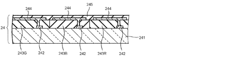
- FIG. 2 is a schematic cross-sectional view of an example of the COA substrate 24 in FIG.
- the COA substrate 24 shown in FIG. 2 includes a light-transmissive insulating substrate 241 such as a glass substrate, and a switching element 242 disposed for each pixel in a region corresponding to an active area on the insulating substrate 241.
- the color filter layers 243R, 243G, and 243B are provided.
- the color filter layers 243R, 243G, and 243B include a plurality of colored layers that are colored red (R), green (G), and blue (B), respectively, and emit light of each color component of red, green, and blue, respectively.
- R red
- G green
- B blue
- the COA substrate further includes a pixel electrode 244 made of a light-transmitting metal material such as ITO connected to the switching element 242. Further, the surfaces of these members are covered with an insulating layer 245 having a high dielectric constant and are flattened.
- an insulating layer 245 having a high dielectric constant and are flattened.
- JP-A 2007-240544, JP-A 2004-163979, JP-A 2008-15375 and the like can be referred to in addition to the above-mentioned Patent Documents 6 and 7.
- the position of the black matrix in the COA liquid crystal display device is preferably located on the COA substrate from the viewpoint of improving the degree of crosslinking of the polymer network. However, since the influence of the black matrix is small, it is disposed on the opposite glass substrate. It may be arranged at any position in the liquid crystal cell.
- FIG. 3 shows a schematic cross-sectional view of an example of the counter substrate 22 in FIG.
- the counter substrate 22 shown in FIG. 3 is made of an insulating substrate having a light transmission property such as a glass substrate, and there is no member that blocks light transmission, such as a color filter layer or an array member. Therefore, if ultraviolet rays are irradiated from the counter substrate 22 side during the formation of the polymer network, the crosslinking reaction can be sufficiently advanced, and the polymer network can be stably formed.
- the counter substrate 22 is not limited to the configuration shown in FIG. 3 and may have any configuration as long as the color filter layer and the array member are not disposed.
- the color filter needs to be arranged on the array substrate.
- the color filter that can be used in the present invention is a plurality of different colors (for example, three primary colors of red, green, and blue light, transparent, yellow, cyan, etc.) in the pixel portion of the substrate, as in the color filter of a normal liquid crystal display device. )
- a coloring material organic pigment, dye, carbon black, etc.
- a colored photosensitive composition which may be colorless
- a layer is formed by coating on a substrate, and a pattern is formed by photolithography.
- the spin coater method is employed in the initial stage, and the slit & spin type coater method is employed from the viewpoint of liquid saving.
- the slit coater method is generally adopted.
- Other methods include roll coating, bar coating, and die coating.
- a pixel color is also formed by an inkjet method.
- methods using a combination of a colored non-photosensitive composition and a photosensitive positive resist, a printing method, an electrodeposition method, and a film transfer method are known.
- the color filter used in the present invention may be produced by any method.
- the material for forming the color filter there are no particular restrictions on the material for forming the color filter.
- the coloring material any of dyes, organic pigments, inorganic pigments and the like can be used. Dyes have been studied due to the demand for higher CR, but in recent years, organic pigment dispersion technology has advanced, and breakdown pigments that have been finely crushed by the salt milling method, etc., and finer pigments by the build-up method have been high. Used for CR conversion. Any coloring material may be used in the present invention. As described above, the color sequential filter is not required in the field sequential drive mode.
- a transparent substrate is preferable, and glass, plastic film, optical crystal, or the like can be used.
- the distance between the pair of substrates is usually about 2 to 100 ⁇ m.
- the applied electric field is usually about 1000 to 100,000 V / cm.
- the electric field may be substantially parallel to the substrate (or perpendicular to the display direction).
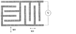
- There is no particular limitation on the method of applying the electric field but a structure in which two comb-shaped electrodes are mutually incorporated on one substrate surface is simple.
- the number of comb teeth per comb-shaped electrode is preferably about 2 to 100, the length is about 1 to 10,000 ⁇ m, the width is about 1 to 50 ⁇ m, and the distance between comb teeth is about 1 to 100 ⁇ m.
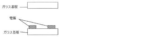
- two comb-shaped electrodes are attached to the substrate so as to be mutually incorporated in the same plane, and by applying a voltage to them, an electric field is applied perpendicular to the comb teeth and parallel to the substrate surface.
- the other substrate is a glass plate without electrodes, and is placed opposite to each other through a spacer such as a thin film.
- a gap with a spacer thickness is formed between the pair of substrates, and the liquid crystal display element LC can be manufactured by injecting a liquid crystal material into the gap.
- the liquid crystal cell LC is arranged between two polarizing plates PL1 and PL2, the absorption axes 10a and 12a of the polarizing plates PL1 and PL2 are orthogonal to each other (so-called crossed Nicols state), and the electric field direction is relative to each absorption axis. If the angle is 45 °, the transmittance is zero when the electric field is zero (because the retardation is zero), and the light is transmitted when the electric field is applied (because the cell in which retardation occurs acts like a wave plate). Therefore, a bright-dark CR can be applied with the voltage ON-OFF. When the retardation of the liquid crystal display element is half of the wavelength of transmitted light, the transmittance is maximized.
- the direction of the long side of the comb electrode of the liquid crystal display element LC is 45 degrees with the absorption axes 10a and 12a of the polarizing plates PL1 and PL2, so that the retardation efficiency is maximized. .
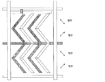
- the configuration of the electrode is two domains in the right half and the left half, and in FIG. 8 described later, two domains can be obtained using a zigzag comb-shaped electrode.
- the electrode structure used in the present invention is not particularly limited as long as it is an electrode structure capable of coplanar switching.
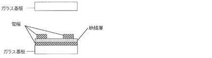
- the electrode structure is such that the common electrode and the pixel electrode are both comb-teeth electrodes, the common electrode and the comb of the surface electrode as shown in the cross-sectional view of FIG.
- An electrode structure in which an insulating layer is sandwiched between the pixel electrode of the tooth electrode may be used.
- FIG. 7A is a cross-sectional view schematically showing a schematic configuration of a main part of the display element according to the present embodiment in an electric field non-application state (OFF state), and FIG. It is sectional drawing which shows typically schematic structure of the principal part of the display element concerning this Embodiment in an ON state.
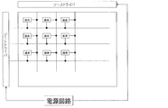
- FIG. 7 is a block diagram showing an example of a schematic configuration of a main part of the display device using the display element according to the present embodiment.
- the display element according to this embodiment is used in a display device together with a drive circuit.
- FIG. 8 includes a display element in which pixels are arranged in a matrix, a source driver and a gate driver as drive circuits, a power supply circuit, and the like.
- the display element is provided with a plurality of data signal lines and a plurality of scanning signal lines intersecting with the data signal lines, and the pixel is provided for each combination of the data signal lines and the scanning signal lines. It has been.
- the power supply circuit supplies a voltage for performing display on the display element to the source driver and the gate driver, whereby the source driver drives a data signal line of the display element, and the gate driver The scanning signal line of the display element is driven.
- a switching element (not shown) is provided.
- the switching element for example, an FET (field effect transistor) or a TFT (thin film transistor) is used, and the gate electrode of the switching element is a scanning signal line, the source electrode is a data signal line, and the drain electrode is It is connected to a pixel electrode (not shown).
- the switching element is turned on, and the signal voltage determined based on the display data signal input from the controller (not shown) is applied to the data signal line by the source driver.
- the display element ideally continues to hold the voltage at the time of interruption while the selection period of the scanning signal line ends and the switching element is interrupted.
- the display element is optically isotropic (macroscopic, specifically, a visible light wavelength region, that is, a wavelength of visible light) when an electric field (voltage) is applied or no electric field (voltage) is applied.
- Display is performed using a medium (a liquid crystalline medium (liquid crystal material), a dielectric substance) indicating a scale or a larger scale.
- the display element shown in FIGS. 7A and 7B includes a pair of substrates disposed as opposed to each other as medium holding means (optical modulation layer holding means), and an optical modulation layer between the pair of substrates. And a medium layer composed of a medium that is optically modulated by application of an electric field (hereinafter referred to as medium A) is sandwiched between the outside of the pair of substrates, that is, the surface opposite to the opposing surfaces of the two substrates.
- the polarizing plate is provided with a polarizing plate.
- At least one substrate has a light-transmitting property, for example, a transparent substrate such as a glass substrate.
- a transparent substrate such as a glass substrate.
- a comb-like comb-like electrode which is an electric field applying means (electric field applying member) for applying an electric field (lateral electric field) substantially parallel to the substrate 1 to the medium layer.
- the comb-tooth portions (comb-tooth electrodes) of the comb-tooth electrodes are disposed so as to face each other.
- zigzag comb electrodes are arranged to face each other.
- the comb electrode is made of an electrode material such as a transparent electrode material such as ITO (indium tin oxide), and is set to have a line width of 5 ⁇ m, a distance between electrodes (electrode interval) of 5 ⁇ m, and a thickness of 0.3 ⁇ m.
- ITO indium tin oxide
- the electrode material, the line width, the distance between the electrodes, and the thickness are merely examples, and are not limited thereto.
- the liquid crystal layer is formed by bonding the substrate provided with the comb electrodes with a sealing agent (not shown) through a spacer such as a plastic bead or a glass fiber spacer (not shown) as necessary. .
- the liquid crystal used in this embodiment is a medium whose degree of optical anisotropy changes when an electric field is applied.
- E j an electric field
- the conventional liquid crystal display element performs display using only the change in the alignment direction due to the rotation of the liquid crystal molecules accompanying the application of an electric field, and the liquid crystal molecules are aligned in a certain direction. Therefore, the inherent viscosity of the liquid crystal greatly affects the response speed.
- the liquid crystal display device of the present embodiment performs display using a change in the degree of optical anisotropy in the medium. Therefore, unlike the conventional liquid crystal display element, there is no problem that the inherent viscosity of the liquid crystal greatly affects the response speed, so that a high-speed response can be realized. Moreover, since it is a high-speed response, it is also preferable to use a field sequential color drive system.
- the field sequential drive method is described in detail in JP-A-2005-181667, JP-A-2009-42446, JP-A-2007-322988, and JP-A-3996178, and can be referred to. .
- a backlight unit that sequentially emits independent three primary color lights is used.
- a backlight unit including an LED as the light source is preferable.
- a backlight unit including an LED element that emits three colors of red, green, and blue as the light source is preferably used.
- the 1st and 2nd transparent films (in FIG. 1, the transparent film 16 and the transparent film 14) used for the liquid crystal display device of this invention are demonstrated.
- the first and second transparent films preferably function as a protective film for the polarizing plate from the viewpoint of thinning the liquid crystal display device. Therefore, polymer films made of various materials used as protective films for polarizing plates can be used.
- the cellulose acylate film has good suitability for polarizing plate processing and is suitable for use as the first and second transparent films. Further, by adding a retardation reducing agent to be described later, a cellulose acylate film satisfying the characteristics required for the first transparent film, that is, low Re and low Rth can be produced. Further, by adding a wavelength dispersion adjusting agent, Re and Rth have appropriate wavelength dispersion characteristics, specifically,
- cellulose as a cellulose acylate raw material examples include cotton linter and wood pulp (hardwood pulp, softwood pulp), and any cellulose acylate obtained from any raw material cellulose may be used. .
- Detailed descriptions of these raw material celluloses can be found, for example, in the course of plastic materials (17) Fibrous resin (by Marusawa and Uda, published by Nikkan Kogyo Shimbun, 1970) and JIII Journal of Technical Disclosure 2001-1745 (page 7). To page 8) can be used, but is not limited thereto.
- Cellulose acylate is an acylated hydroxyl group of cellulose.
- the acyl group may be any acyl group having 2 to 22 carbon atoms.
- the degree of substitution with a hydroxyl group in cellulose is not particularly limited, but the degree of substitution can be obtained by measuring the degree of binding of acetic acid and / or a fatty acid having 3 to 22 carbon atoms to substitute for the hydroxyl group of cellulose. As a measuring method, it can be carried out according to ASTM D-817-91.
- the degree of substitution of the cellulose with a hydroxyl group is not particularly limited, but the degree of acyl substitution with the hydroxyl group of cellulose is preferably 2.00 to 3.00. Furthermore, the substitution degree is more preferably 2.75 to 3.00, and further preferably 2.85 to 3.00.
- the acyl group having 2 to 22 carbon atoms may be an aliphatic group or an allyl group, and may be a single type or a mixture of two or more types. Good. Examples thereof include cellulose alkylcarbonyl ester, alkenylcarbonyl ester, aromatic carbonyl ester and aromatic alkylcarbonyl ester. Each of these may further have a substituted group.
- acyl groups acetyl group, propionyl group, butanoyl group, heptanoyl group, hexanoyl group, octanoyl group, decanoyl group, dodecanoyl group, tridecanoyl group, tetradecanoyl group, hexadecanoyl group, octadecanoyl group And iso-butanoyl group, tert-butanoyl group, cyclohexanecarbonyl group, oleoyl group, benzoyl group, naphthylcarbonyl group, cinnamoyl group and the like.
- acetyl group, propionyl group, butanoyl group, dodecanoyl group, octadecanoyl group, tert-butanoyl group, oleoyl group, benzoyl group, naphthylcarbonyl group, cinnamoyl group and the like are preferable, and acetyl group, propionyl group, butanoyl group are preferable. Groups are more preferred.
- the total substitution degree is 2.50 to 3.00
- the optical anisotropy of the cellulose acylate film can be reduced. Therefore, for the production of the cellulose acylate film used as the first transparent film, it is preferable to use cellulose acylate having an acyl substitution degree of 2.60 to 3.00 as a raw material, and an acyl substitution degree of 2.65 to More preferably, 3.00 cellulose acylate is used.
- the type of the substituent that the cellulose acylate used as the raw material of the cellulose acylate film used as the second transparent film has and the degree of substitution will be determined according to the required optical properties.
- cellulose acylate containing an aromatic group such as a phenyl group can be used.
- the degree of polymerization of cellulose acylate is preferably 180 to 700 in terms of viscosity average degree of polymerization, more preferably 180 to 550, more preferably 180 to 400, and particularly preferably 180 to 350 for cellulose acetate.
- the degree of polymerization can be measured, for example, by the intrinsic viscosity method of Uda et al.
- Mw is a mass average molecular weight
- Mn is a number average molecular weight
- the specific value of Mw / Mn is preferably 1.0 to 3.0, more preferably 1.0 to 2.0, and more preferably 1.0 to 1.6. Further preferred.
- the average molecular weight (polymerization degree) increases, but the viscosity is lower than that of normal cellulose acylate, which is useful.
- Cellulose acylate having a small amount of low molecular components can be obtained by removing low molecular components from cellulose acylate synthesized by a usual method. The removal of the low molecular component can be carried out by washing the cellulose acylate with an appropriate organic solvent.
- the amount of sulfuric acid catalyst in the acetylation reaction is preferably adjusted to 0.5 to 25 parts by mass with respect to 100 parts by mass of cellulose.
- cellulose acylate that is preferable in terms of molecular weight distribution (uniform molecular weight distribution) can be synthesized.
- the water content is preferably 2% by mass or less, more preferably 1% by mass or less, and particularly 0.7% by mass. It is a cellulose acylate having a moisture content of not more than%.
- cellulose acylate contains water and is known to be 2.5 to 5% by mass. In order to make the moisture content of a cellulose acylate into the said range, it is necessary to dry, and the method will not be specifically limited if it becomes the target moisture content.
- Cellulose acylate is described in detail on pages 7 to 12 of the raw material cotton and the synthesis method in the Japan Society for Invention and Technology (Publication No. 2001-1745, published on March 15, 2001, Japan Society for Invention). .
- a single or a mixture of two or more different cellulose acylates can be used.
- cellulose acylate film select from various additives (for example, compounds that reduce optical anisotropy, wavelength dispersion adjusters, UV inhibitors, plasticizers, deterioration inhibitors, fine particles, optical property adjusters, etc.) At least one of the above can be added.
- compounds that reduce optical anisotropy include compounds that satisfy the following formula.
- Rth (A) represents Rth (nm) of a film containing A% of a compound that decreases optical anisotropy
- Rth (0) is the film, and decreases optical anisotropy.
- Rth (nm) of a film not containing a compound is represented, and A represents the mass (%) of a compound that reduces optical anisotropy when the mass of the film raw material polymer is 100.
- the compound that reduces the optical anisotropy more preferably satisfies the following formula. (Rth (A) ⁇ Rth (0) ) /A ⁇ 2.0 0.1 ⁇ A ⁇ 20
- the compound that lowers the optical anisotropy is preferably selected from compounds that are sufficiently compatible with cellulose acylate and do not have a rod-like structure or planar structure. Specifically, when having a plurality of planar functional groups such as aromatic groups, a compound having a structure in which these functional groups are not on the same plane but on a non-planar surface is preferable.
- the optical anisotropy is reduced by suppressing the cellulose acylate in the film from being oriented in the plane and in the film thickness direction as described above.
- compounds having an octanol-water partition coefficient (log P value) of 0 to 7 are preferably used.
- a compound having a log P value of 7 or less compatibility with cellulose acylate is improved, and the cloudiness and powder blowing of the film can be more effectively prevented.
- the hydrophilicity is high by adopting a compound having a log P value of 0 or more, it is possible to more effectively prevent the water resistance of the cellulose acetate film from deteriorating.
- a more preferable range of the logP value is 1 to 6, and a particularly preferable range is 1.5 to 5.
- the octanol-water partition coefficient (log P value) can be measured by a flask immersion method described in JIS Japanese Industrial Standard Z7260-107 (2000).
- the octanol-water partition coefficient (log P value) can be estimated by a computational chemical method or an empirical method instead of the actual measurement.
- Crippen's fragmentation method J. Chem. Inf. Comput. Sci., 27, 21 (1987).
- Viswanadhan's fragmentation method J. Chem. Inf. Comput. Sci., 29, 163 (1989).
- Broto's fragmentation method Eur. J. Med. Chem.-Chim. Theor., 19, 71 (1984).
- Crippen's fragmentation method J. Chem. Inf. Comput. Sci., 27 , 21 (1987).
- the log P value of a certain compound varies depending on the measurement method or calculation method, it is preferable to determine whether or not the compound is within the scope of the present invention by the Crippen's fragmentation method.
- the compound that reduces optical anisotropy may or may not contain an aromatic group.
- the compound that reduces optical anisotropy preferably has a molecular weight of 150 to 3000, more preferably 170 to 2000, and even more preferably 200 to 1000. As long as these molecular weights are within the range, a specific monomer structure may be used, or an oligomer structure or a polymer structure in which a plurality of the monomer units are bonded may be used.
- the compound that reduces optical anisotropy is preferably a liquid at a temperature of 25 ° C. or a solid having a melting point of 25 to 250 ° C., more preferably a liquid at a temperature of 25 ° C. or a melting point of 25 to 25 ° C.
- the compound which reduces optical anisotropy does not volatilize in the process of dope casting for cellulose acylate film production and drying.
- the amount of the compound that decreases the optical anisotropy is preferably 0.01 to 30% by mass, more preferably 1 to 25% by mass, and more preferably 5 to 20% by mass of the cellulose acylate. Is particularly preferred.
- the compound that decreases the optical anisotropy may be used alone, or two or more compounds may be mixed and used in an arbitrary ratio.
- the timing for adding the compound for reducing the optical anisotropy may be any time during the dope preparation process, or may be performed at the end of the dope preparation process.
- the compound that reduces the optical anisotropy is such that the average content of the compound in the portion from the surface on at least one side to 10% of the total film thickness is the average content of the compound in the central portion of the cellulose acylate film. 80-99% of The amount of the compound that reduces the optical anisotropy can be determined by measuring the amount of the compound at the surface and in the central portion, for example, by a method using an infrared absorption spectrum described in JP-A-8-57879.
- a first example of a compound that reduces optical anisotropy is a compound represented by the following general formula (13).
- R 11 represents an alkyl group or an aryl group
- R 12 and R 13 each independently represent a hydrogen atom, an alkyl group, or an aryl group. Further, it is particularly preferable that the total number of carbon atoms of R 11 , R 12 and R 13 is 10 or more.
- R 11 , R 12 and R 13 may have a substituent, and the substituent is preferably a fluorine atom, an alkyl group, an aryl group, an alkoxy group, a sulfone group or a sulfonamide group, an alkyl group, an aryl group, Alkoxy groups, sulfone groups and sulfonamido groups are particularly preferred.
- the alkyl group may be linear, branched or cyclic, and preferably has 1 to 25 carbon atoms, more preferably 6 to 25, and more preferably 6 to 20 (For example, methyl, ethyl, propyl, isopropyl, butyl, isobutyl, t-butyl, amyl, isoamyl, t-amyl, hexyl, cyclohexyl, heptyl, octyl, bicyclo Octyl, nonyl, adamantyl, decyl, t-octyl, undecyl, dodecyl, tridecyl, tetradecyl, pentadecyl, hexadecyl, heptadecyl, octadecyl, nonadecyl, didecyl) are particularly preferred .
- aryl group those having 6 to 30 carbon atoms are preferable, and those having 6 to 24 carbon atoms (for example, phenyl group, biphenyl group, terphenyl group, naphthyl group, binaphthyl group, triphenylphenyl group) are particularly preferable.
- phenyl group, biphenyl group, terphenyl group, naphthyl group, binaphthyl group, triphenylphenyl group are particularly preferable.
- Pr i means an isopropyl group (hereinafter the same).
- Examples of the compound that reduces the optical anisotropy include a compound represented by the following general formula (18).
- R 14 represents an alkyl group or an aryl group
- R 15 and R 16 each independently represent a hydrogen atom, an alkyl group, or an aryl group.
- R 14 is preferably a phenyl group or a cyclic alkyl group.
- R 15 and R 16 are each preferably a phenyl group or an alkyl group.
- As the alkyl group both a cyclic alkyl group and a linear alkyl group are preferable.
- These groups may have a substituent, and the substituent is preferably a fluorine atom, an alkyl group, an aryl group, an alkoxy group, a sulfone group, or a sulfonamide group, and an alkyl group, an aryl group, an alkoxy group, a sulfone group.
- Groups and sulfonamido groups are particularly preferred.
- the compound represented by the general formula (18) is more preferably a compound represented by the general formula (19).
- R 114 , R 115 and R 116 each independently represents an alkyl group or an aryl group.
- the alkyl group is preferably a cyclic alkyl group or a linear alkyl group
- the aryl group is preferably a phenyl group.
- Bu i means an isobutyl group.
- wavelength dispersion adjusting agent a compound that lowers the wavelength dispersion of retardation
- ⁇ Rth
- ⁇ Rth (B) means ⁇ Rth of the film containing B mass% of the wavelength dispersion adjusting agent
- ⁇ Rth (0) is the wavelength dispersion adjustment. It means ⁇ Rth of the same film containing no agent.
- the wavelength dispersion adjusting agent satisfies the following formula. ( ⁇ Rth (B) ⁇ Rth (0)) / B ⁇ ⁇ 3.0 0.05 ⁇ B ⁇ 25 Further, it is more preferable that the wavelength dispersion adjusting agent satisfies the following formula. ( ⁇ Rth (B) ⁇ Rth (0)) / B ⁇ ⁇ 4.0 0.1 ⁇ B ⁇ 20
- the above-mentioned wavelength dispersion adjusting agent is a compound having absorption in the ultraviolet region of 200 to 400 nm and capable of reducing
- the Re and Rth values of the cellulose acylate film generally have wavelength dispersion characteristics that are larger on the long wavelength side than on the short wavelength side. Accordingly, it is required to make the wavelength dispersion smooth by increasing Re and Rth on the relatively small short wavelength side.
- a compound having absorption in the ultraviolet region with a wavelength of 200 to 400 nm has a wavelength dispersion characteristic that the absorbance on the long wavelength side is larger than that on the short wavelength side. If this compound itself is isotropically present inside the cellulose acylate film, it is assumed that the birefringence of the compound itself, and thus the wavelength dispersion of Re and Rth, is large on the short wavelength side as well as the wavelength dispersion of absorbance.
- Re and Rth of the cellulose acylate film are used.
- the compound used as the wavelength dispersion adjusting agent is required to be sufficiently uniformly compatible with cellulose acylate.
- the absorption band range in the ultraviolet region of such a compound is preferably 200 to 400 nm, more preferably 220 to 395 nm, and further preferably 240 to 390 nm.
- the compound used as the wavelength dispersion adjusting agent is required not to increase the spectral transmittance of the cellulose acylate film.
- the cellulose acylate film used as a transparent film in the present invention preferably has a spectral transmittance of 45% to 95% at a wavelength of 380 nm, and preferably has a spectral transmittance of 10% or less at a wavelength of 350 nm.
- the chromatic dispersion adjusting agent is preferably not volatilized in the dope casting and drying processes.
- the wavelength dispersion adjusting agent preferably has a molecular weight of 250 to 1000, more preferably 260 to 800, still more preferably 270 to 800, and particularly preferably 300 to 800.
- a specific monomer structure may be used as long as these molecular weights are within the range, and an oligomer structure or a polymer structure in which a plurality of the monomer units are bonded may be used.
- the addition amount of the wavelength dispersion adjusting agent is preferably 0.01 to 30% by mass, more preferably 0.1 to 20% by mass, and more preferably 0.2 to 10% by mass with respect to cellulose acylate. % Is particularly preferred.
- These wavelength dispersion adjusting agents may be used alone or in combination of two or more compounds at an arbitrary ratio.
- the timing for adding these wavelength dispersion adjusting agents may be any time during the dope production process, or at the end of the dope preparation process. Good.
- wavelength dispersion adjusting agent examples include, but are not limited to, benzotriazole compounds, benzophenone compounds, compounds containing a cyano group, oxybenzophenone compounds, salicylic acid ester compounds, nickel complex compounds, and the like. It is not something.
- Q 11 represents a nitrogen-containing aromatic heterocycle, preferably a 5- to 7-membered nitrogen-containing aromatic heterocycle, more preferably a 5- or 6-membered nitrogen-containing aromatic heterocycle, , Imidazole ring, pyrazole ring, triazole ring, tetrazole ring, thiazole ring, oxazole ring, selenazole ring, benzotriazole ring, benzothiazole ring, benzoxazole ring, benzoselenazole ring, thiadiazole ring, oxadiazole ring, naphthothiazole ring Naphthoxazole ring, azabenzimidazole ring, purine ring, pyridine ring, pyrazine ring, pyrimidine ring, pyridazine ring, triazine ring, triazaindene ring, tetrazaindene ring, and the like, more preferably a
- Nitrogen-containing aromatic heterocycle specifically imidazole ring, pyrazo Le ring, triazole ring, tetrazole ring, thiazole ring, oxazole ring, benzotriazole ring, benzothiazole ring, benzoxazole ring, thiadiazole ring, oxadiazole ring are preferred, particularly preferably a benzotriazole ring.
- the aromatic ring represented by Q 12 may be an aromatic hydrocarbon ring or an aromatic heterocycle. These may be monocyclic or may form a condensed ring with another ring.
- the aromatic hydrocarbon ring is preferably a monocyclic or bicyclic aromatic hydrocarbon ring having 6 to 30 carbon atoms, more preferably a monocyclic or bicyclic aromatic hydrocarbon ring having 6 to 20 carbon atoms. More preferably a monocyclic or bicyclic aromatic hydrocarbon ring having 6 to 12 carbon atoms, and most preferably a benzene ring.
- the aromatic heterocycle is preferably an aromatic heterocycle containing a nitrogen atom or a sulfur atom.
- hetero ring examples include, for example, thiophene ring, imidazole ring, pyrazole ring, pyridine ring, pyrazine ring, pyridazine ring, triazole ring, triazine ring, indole ring, indazole ring, purine ring, thiazoline ring, thiazole ring, thiadiazole.
- the aromatic hetero ring is preferably a pyridine ring, a triazine ring or a quinoline ring.
- the aromatic ring represented by Q 12 is preferably an aromatic hydrocarbon ring, more preferably a naphthalene ring or a benzene ring, and particularly preferably a benzene ring.
- Q 11 and Q 12 may each have a substituent, and the substituent T described below is preferable as the substituent.
- the substituent T include an alkyl group (preferably having 1 to 20 carbon atoms, more preferably 1 to 12 carbon atoms, and particularly preferably 1 to 8 carbon atoms.
- a group (preferably having 6 to 30 carbon atoms, more preferably 6 to 20 carbon atoms, particularly preferably 6 to 12 carbon atoms, and examples thereof include a phenyl group, a p-methylphenyl group, and a naphthyl group), Or an unsubstituted amino group (preferably having 0 to 20 carbon atoms, more preferably 0 to 10 carbon atoms, particularly preferably 0 to 6 carbon atoms, such as an amino group, a methylamino group, a dimethylamino group, a diethylamino group, Dibenzylamino group, etc.), alkoxy groups (preferably having 1 to 20 carbon atoms, more preferably 1 to 12 carbon atoms, particularly preferably 1 to 8 carbon atoms, such as methoxy group, ethoxy group, butoxy group) Groups), aryloxy groups (preferably having 6 to 20 carbon atoms, more preferably 6 to 16 carbon atoms, and particularly preferably 6 to 12 carbon atoms
- a phenyloxy group, a 2-naphthyloxy group, etc. an acyl group (preferably having 1 to 20 carbon atoms, more preferably 1 to 16 carbon atoms, particularly preferably 1 to 12 carbon atoms, Acetyl group, benzoyl group, formyl group, pivaloyl group, etc.), alkoxycarbonyl group (preferably having 2 to 20 carbon atoms, more preferably 2 to 16 carbon atoms, particularly preferably 2 to 12 carbon atoms)
- an aryloxycarbonyl group preferably having a carbon number of 7 to 20, more preferably a carbon number of 7 to 16, particularly preferably a carbon number of 7 to 10, such as phenyl Oxycarbonyl group, etc.
- acyloxy group preferably having 2 to 20 carbon atoms, more preferably carbon It has a prime number of 2 to 16, particularly preferably 2 to 10 carbon
- An acylamino group (preferably having 2 to 20 carbon atoms, more preferably 2 to 16 carbon atoms, particularly preferably 2 to 10 carbon atoms, such as acetylamino group and benzoylamino group), alkoxycarbonyl
- An amino group (preferably having 2 to 20 carbon atoms, more preferably 2 to 16 carbon atoms, particularly preferably 2 to 12 carbon atoms, such as a methoxycarbonylamino group), an aryloxycarbonylamino group (preferably Has 7 to 20 carbon atoms, more preferably 7 to 16 carbon atoms, particularly preferably 7 to 12 carbon atoms, such as a phenyloxycarbonylamino group, and a sulfonylamino group (preferably 1 to 1 carbon atom).
- sulfamoyl group (preferably having 0 to 20 carbon atoms, more preferably 0 to 16 carbon atoms, particularly preferably 0 to 12 carbon atoms, such as sulfamoyl group, methyl A sulfamoyl group, a dimethylsulfamoyl group, a phenylsulfamoyl group, etc.), a carbamoyl group (preferably having 1 to 20 carbon atoms, more preferably 1 to 16 carbon atoms, and particularly preferably 1 to carbon atoms).
- Examples thereof include a carbamoyl group, a methylcarbamoyl group, a diethylcarbamoyl group, a phenylcarbamoyl group, etc.), an alkylthio group (preferably having 1 to 20 carbon atoms, more preferably 1 to 16 carbon atoms, and particularly preferably carbon atoms). And examples thereof include a methylthio group and an ethylthio group.
- An arylthio group (preferably having 6 to 20 carbon atoms, more preferably 6 to 16 carbon atoms, particularly preferably 6 to 12 carbon atoms, such as a phenylthio group), a sulfonyl group (preferably 1 to 20 carbon atoms, more preferably 1 to 16 carbon atoms, particularly preferably 1 to 12 carbon atoms, such as mesyl group and tosyl group), sulfinyl group (preferably 1 to 20 carbon atoms, More preferably, it has 1 to 16 carbon atoms, particularly preferably 1 to 12 carbon atoms, such as methanesulfinyl group, benzenesulfinyl group, etc.), ureido group (preferably 1 to 20 carbon atoms, more preferably carbon The number is 1 to 16, particularly preferably 1 to 12, and examples thereof include a ureido group, a methylureido group, and a phenylureido group.
- Phosphoric acid amide groups preferably having 1 to 20 carbon atoms, more preferably 1 to 16 carbon atoms, particularly preferably 1 to 12 carbon atoms, and examples thereof include diethyl phosphoric acid amide and phenyl phosphoric acid amide.
- halogen atom eg fluorine atom, chlorine atom, bromine atom, iodine atom
- cyano group eg fluorine
- a silyl group (preferably having 3 to 40 carbon atoms, more preferably 3 to 30 carbon atoms, particularly preferably 3 to 24 carbon atoms, and examples thereof include a trimethylsilyl group and a triphenylsilyl group. ) And the like. These substituents may be further substituted. Moreover, when there are two or more substituents, they may be the same or different. If possible, they may be linked together to form a ring.
- the compounds represented by the general formula (101) are preferable.
- R 1 , R 2 , R 3 , R 4 , R 5 , R 6 , R 7 and R 8 each independently represents a hydrogen atom or a substituent.
- R 1 , R 2 , R 3 , R 4 , R 5 , R 6 , R 7 , R 8 , and R 9 each independently represent a hydrogen atom or a substituent, and the above-mentioned substituent T is applied as the substituent. it can. These substituents may be further substituted with another substituent, and the substituents may be condensed to form a ring structure.
- R 1 and R 3 are each preferably a hydrogen atom, an alkyl group, an alkenyl group, an alkynyl group, an aryl group, an amino group, an alkoxy group, an aryloxy group, a hydroxy group, or a halogen atom, more preferably a hydrogen atom.
- An alkyl group, an aryl group, an alkyloxy group, an aryloxy group and a halogen atom more preferably a hydrogen atom and an alkyl group having 1 to 12 carbon atoms, particularly preferably an alkyl group having 1 to 12 carbon atoms (preferably a carbon atom). 4 to 12).
- R 2 and R 4 are each preferably a hydrogen atom, an alkyl group, an alkenyl group, an alkynyl group, an aryl group, an amino group, an alkoxy group, an aryloxy group, a hydroxy group, or a halogen atom, more preferably a hydrogen atom.
- An alkyl group, an aryl group, an alkyloxy group, an aryloxy group, and a halogen atom more preferably a hydrogen atom and an alkyl group having 1 to 12 carbon atoms, particularly preferably a hydrogen atom and a methyl group, and most preferably a hydrogen atom. Is an atom.
- R 5 and R 8 are each preferably a hydrogen atom, an alkyl group, an alkenyl group, an alkynyl group, an aryl group, an amino group, an alkoxy group, an aryloxy group, a hydroxy group, or a halogen atom, more preferably a hydrogen atom.
- An alkyl group, an aryl group, an alkyloxy group, an aryloxy group, and a halogen atom more preferably a hydrogen atom and an alkyl group having 1 to 12 carbon atoms, particularly preferably a hydrogen atom and a methyl group, and most preferably a hydrogen atom. Is an atom.
- R 6 and R 7 are each preferably a hydrogen atom, an alkyl group, an alkenyl group, an alkynyl group, an aryl group, an amino group, an alkoxy group, an aryloxy group, a hydroxy group, or a halogen atom, more preferably a hydrogen atom.
- An alkyl group, an aryl group, an alkyloxy group, an aryloxy group and a halogen atom more preferably a hydrogen atom and a halogen atom, and particularly preferably a hydrogen atom and a chlorine atom.
- the compounds represented by the general formula (101) are preferable.
- R 1 , R 3 , R 6 and R 7 have the same meanings as those in formula (101-A), respectively, and the preferred ranges are also the same.
- examples of the benzophenone-based compound that can be used as the wavelength dispersion adjusting agent include a compound represented by the general formula (102).
- Q 1 and Q 2 each represent an aromatic ring.
- X represents NR (R represents a hydrogen atom or a substituent), an oxygen atom, or a sulfur atom.
- the aromatic ring represented by Q 1 or Q 2 may be an aromatic hydrocarbon ring or an aromatic heterocycle. These may be monocyclic or may form a condensed ring with another ring.
- the aromatic hydrocarbon ring represented by Q 1 and Q 2 is preferably (preferably a monocyclic or bicyclic aromatic hydrocarbon ring having 6 to 30 carbon atoms (for example, a benzene ring, a naphthalene ring, etc.). More preferably, it is an aromatic hydrocarbon ring having 6 to 20 carbon atoms, and further preferably an aromatic hydrocarbon ring having 6 to 12 carbon atoms.) More preferably, it is a benzene ring.
- the aromatic heterocycle represented by Q 1 and Q 2 is preferably an aromatic heterocycle containing at least one of an oxygen atom, a nitrogen atom or a sulfur atom.
- the heterocyclic ring include, for example, furan ring, pyrrole ring, thiophene ring, imidazole ring, pyrazole ring, pyridine ring, pyrazine ring, pyridazine ring, triazole ring, triazine ring, indole ring, indazole ring, purine ring, thiazoline.
- the aromatic hetero ring is preferably a pyridine ring, a triazine ring or a quinoline ring.
- the aromatic ring represented by Q 1 or Q 2 is preferably an aromatic hydrocarbon ring, more preferably an aromatic hydrocarbon ring having 6 to 10 carbon atoms, and further preferably a substituted or unsubstituted benzene. It is a ring.
- Q 1 or Q 2 may further have a substituent, and the above-described substituent T is preferable, but the substituent does not contain a carboxylic acid, a sulfonic acid, or a quaternary ammonium salt. Further, if possible, substituents may be linked to form a ring structure.
- X represents NR (R represents a hydrogen atom or a substituent.
- substituent the above-mentioned substituent T can be applied
- an oxygen atom or a sulfur atom X is preferably NR (R is preferably an acyl group) , A sulfonyl group, and these substituents may be further substituted.)
- an oxygen atom particularly preferably an oxygen atom.
- R 21 , R 22 , R 23 , R 24 , R 25 , R 26 , R 27 , R 28 , and R 29 each independently represent a hydrogen atom or a substituent.
- R 21 , R 23 , R 24 , R 25 , R 26 , R 28 , and R 29 each independently represent a hydrogen atom or a substituent, and the substituent T described above can be applied as the substituent. These substituents may be further substituted with another substituent, and the substituents may be condensed to form a ring structure.
- R 21 , R 23 , R 24 , R 25 , R 26 , R 28 , and R 29 are preferably a hydrogen atom, alkyl group, alkenyl group, alkynyl group, aryl group, amino group, alkoxy group, aryloxy group , A hydroxy group, and a halogen atom, more preferably a hydrogen atom, an alkyl group, an aryl group, an alkyloxy group, an aryloxy group, and a halogen atom, still more preferably a hydrogen atom and a carbon 1-12 alkyl group, Preferred are a hydrogen atom and a methyl group, and most preferred is a hydrogen atom.
- R 22 is preferably a hydrogen atom, an alkyl group, an alkenyl group, an alkynyl group, an aryl group, an amino group, an alkoxy group, an aryloxy group, a hydroxy group, or a halogen atom, more preferably a hydrogen atom or a carbon number of 1 to 20
- R 27 is preferably a hydrogen atom, an alkyl group, an alkenyl group, an alkynyl group, an aryl group, an amino group, an alkoxy group, an aryloxy group, a hydroxy group, a halogen atom, more preferably a hydrogen atom or an alkyl group having 1 to 20 carbon atoms.
- R 10 represents a hydrogen atom, an alkyl group, an alkenyl group, an alkynyl group, or an aryl group.
- R 10 represents a hydrogen atom, an alkyl group, an alkenyl group, an alkynyl group, or an aryl group, and these may have a substituent.
- substituent the above-described substituent T can be applied.
- R 10 is preferably an alkyl group, more preferably an alkyl group having 5 to 20 carbon atoms, and still more preferably an alkyl group having 5 to 12 carbon atoms (n-hexyl group, 2-ethylhexyl group, n-octyl group).
- n-decyl group, n-dodecyl group, benzyl group, etc. particularly preferably a substituted or unsubstituted alkyl group having 6 to 12 carbon atoms (2-ethylhexyl group, n-octyl group). N-decyl group, n-dodecyl group, benzyl group).
- the compound represented by the general formula (102) can be synthesized by a known method described in JP-A-11-12219. Specific examples of the compound represented by the general formula (102) are given below, but the present invention is not limited to the following specific examples.
- examples of the compound containing a cyano group that can be used as the wavelength dispersion adjusting agent used in the present invention include a compound represented by the general formula (103).
- Q 31 and Q 32 each independently represents an aromatic ring.
- X 31 and X 32 each represent a hydrogen atom or a substituent, and at least one of them represents a cyano group, a carbonyl group, a sulfonyl group, or an aromatic heterocycle.
- the aromatic ring represented by Q 31 and Q 32 may be an aromatic hydrocarbon ring or an aromatic heterocycle. These may be monocyclic or may form a condensed ring with another ring.
- the aromatic hydrocarbon ring is preferably a monocyclic or bicyclic aromatic hydrocarbon ring having 6 to 30 carbon atoms (for example, benzene ring, naphthalene ring, etc.), more preferably 6 to 20 carbon atoms.
- the aromatic heterocycle is preferably an aromatic heterocycle containing a nitrogen atom or a sulfur atom.
- the hetero ring include, for example, thiophene ring, imidazole ring, pyrazole ring, pyridine ring, pyrazine ring, pyridazine ring, triazole ring, triazine ring, indole ring, indazole ring, purine ring, thiazoline ring, thiazole ring, thiadiazole.
- the aromatic hetero ring is preferably a pyridine ring, a triazine ring or a quinoline ring.
- the aromatic ring represented by Q 31 and Q 32 is preferably an aromatic hydrocarbon ring, more preferably a benzene ring.
- Q 31 and Q 32 may further have a substituent, and the above-described substituent T is preferable.
- X 31 and X 32 each represent a hydrogen atom or a substituent, and at least one of them represents a cyano group, a carbonyl group, a sulfonyl group, or an aromatic heterocycle.
- the substituent T described above can be applied to the substituents represented by X 31 and X 32 .
- the substituent represented by X 31 and X 32 may be further substituted with another substituent, and X 31 and X 32 may each be condensed to form a ring structure.
- X 31 and X 32 are preferably a hydrogen atom, an alkyl group, an aryl group, a cyano group, a nitro group, a carbonyl group, a sulfonyl group, or an aromatic heterocycle, and more preferably a cyano group, a carbonyl group, a sulfonyl group, An aromatic heterocycle, more preferably a cyano group or a carbonyl group, and particularly preferably a cyano group or an alkoxycarbonyl group (—C ( ⁇ O) OR (R is an alkyl group having 1 to 20 carbon atoms, 6 carbon atoms). To 12 aryl groups and combinations thereof).
- the compounds represented by the general formula (103) are preferable.
- R 31 , R 32 , R 33 , R 34 , R 35 , R 36 , R 37 , R 38 , R 39 and R 30 each independently represent a hydrogen atom or a substituent.
- X 31 and X 32 have the same meanings as those in formula (103), and preferred ranges are also the same.
- R 31 , R 32 , R 34 , R 35 , R 36 , R 37 , R 39 and R 30 each independently represent a hydrogen atom or a substituent, and the substituent T described above can be applied as the substituent. These substituents may be further substituted with another substituent, and the substituents may be condensed to form a ring structure.
- R 31 , R 32 , R 34 , R 35 , R 36 , R 37 , R 39 and R 30 are preferably a hydrogen atom, an alkyl group, an alkenyl group, an alkynyl group, an aryl group, an amino group, an alkoxy group, an aryloxy group Group, hydroxy group and halogen atom, more preferably hydrogen atom, alkyl group, aryl group, alkyloxy group, aryloxy group and halogen atom, still more preferably hydrogen atom and carbon 1-12 alkyl group, Particularly preferred are a hydrogen atom and a methyl group, and most preferred is a hydrogen atom.
- R 33 and R 38 are preferably a hydrogen atom, an alkyl group, an alkenyl group, an alkynyl group, an aryl group, an amino group, an alkoxy group, an aryloxy group, a hydroxy group, or a halogen atom, more preferably a hydrogen atom or a carbon number.
- the general formula (103) is more preferably a compound represented by the following general formula (103-B).
- R 33 and R 38 have the same meanings as those in the general formula (103-A), and preferred ranges are also the same.
- X 33 represents a hydrogen atom or a substituent.
- X 33 represents a hydrogen atom or a substituent.
- the substituent the above-described substituent T can be applied, and if possible, the substituent may be further substituted with a substituent.
- X 33 is preferably a hydrogen atom, an alkyl group, an aryl group, a cyano group, a nitro group, a carbonyl group, a sulfonyl group or an aromatic heterocycle, more preferably a cyano group, a carbonyl group, a sulfonyl group or an aromatic heterocycle.
- a ring more preferably a cyano group or a carbonyl group, and particularly preferably a cyano group or an alkoxycarbonyl group (—C ( ⁇ O) OR 301 (R 301 is an alkyl group having 1 to 20 carbon atoms, 6 to 6 carbon atoms). 12 aryl groups and combinations thereof)).
- More preferred as the general formula (103) is a compound represented by the general formula (103-C).
- R 33 and R 38 have the same meanings as those in general formula (103-A), and preferred ranges thereof are also the same.
- R 302 represents an alkyl group having 1 to 20 carbon atoms.
- R 302 is preferably an alkyl group having 2 to 12 carbon atoms, more preferably an alkyl group having 4 to 12 carbon atoms, and more preferably when both R 33 and R 38 are hydrogen atoms, An alkyl group having 6 to 12 carbon atoms, particularly preferably an n-octyl group, a tert-octyl group, a 2-ethylhexyl group, an n-decyl group or an n-dodecyl group, most preferably 2-ethyl Hexyl group.
- R 302 is preferably an alkyl group having a molecular weight of 300 or more and a carbon number of 20 or less and a compound represented by the general formula (103-C) when R 33 and R 38 are other than hydrogen. Is preferred.
- the compound represented by the general formula (103) can be synthesized by the method described in Journal of American Chemical Society 63, page 3452 (1941).
- Examples of the cellulose acylate film for the second transparent film include an optically biaxial or uniaxial film as described above.
- a retardation increasing agent As an additive having an action of increasing the retardation of a cellulose acylate film (retardation developing agent), rod-like aromatic compounds described on pages 11 to 14 of JP-A-2004-50516 can be preferably used.
- Examples of compounds that can be used as a retardation increasing agent for cellulose acylate films include the compounds described in JP-A-2002-277632, [0016] to [0024].
- Examples of compounds that can be used as a retardation increasing agent for cellulose acylate films include the compounds described in JP-A-2002-182215, [0033] to [0041].
- the retardation increasing agent can be used alone or in combination of two or more.
- the addition amount of the retardation enhancer is preferably 0.1 to 20% by mass, more preferably 0.5 to 10% by mass with respect to 100% by weight of cellulose acylate.
- Fine particles usable in the present invention include silicon dioxide (silica), titanium dioxide, aluminum oxide, zirconium oxide, calcium carbonate, calcium carbonate, talc, clay, calcined kaolin, calcined calcium silicate, hydrated calcium silicate, silicic acid. Mention may be made of aluminum, magnesium silicate and calcium phosphate. Among these fine particles, those containing silicon are preferable in terms of low turbidity, and silicon dioxide is more preferable.
- the fine particles of silicon dioxide preferably have a primary average particle size of 1 nm to 20 nm and an apparent specific gravity of 70 g / liter or more.
- a primary particle having an average diameter of 5 to 25 nm is more preferred because it can reduce the haze of the film.
- the apparent specific gravity is preferably 90 to 200 g / liter or more, and more preferably 100 to 200 g / liter or more. A larger apparent specific gravity is preferable because a high-concentration dispersion can be produced, and haze and aggregates are improved.
- These fine particles usually form secondary particles having an average particle size of 0.05 to 2.0 ⁇ m, and these fine particles are present in the film as aggregates of primary particles, and 0.05 ⁇ m on the film surface. Irregularities of up to 2.0 ⁇ m are formed.
- the secondary average particle size is preferably 0.05 ⁇ m to 1.0 ⁇ m, more preferably 0.1 ⁇ m to 0.7 ⁇ m, and even more preferably 0.1 ⁇ m to 0.4 ⁇ m.
- the primary or secondary particle size was determined by observing the particles in the film with a scanning electron microscope and determining the diameter of a circle circumscribing the particles as the particle size. Also, 200 particles are observed at different locations, and the average value is taken as the average particle size.
- silicon dioxide fine particles for example, commercially available products such as Aerosil R972, R972V, R974, R812, 200, 200V, 300, R202, OX50, TT600 (manufactured by Nippon Aerosil Co., Ltd.) can be used.
- Zirconium oxide fine particles are commercially available, for example, under the trade names Aerosil R976 and R811 (manufactured by Nippon Aerosil Co., Ltd.), and can be used.
- Aerosil 200V and Aerosil R972V are fine particles of silicon dioxide having a primary average particle size of 20 nm or less and an apparent specific gravity of 70 g / liter or more, and the coefficient of friction is maintained while keeping the haze of the optical film low. It is particularly preferable because it has a great effect of reducing the effect.
- the mixing method of the matting agent is not particularly limited, but it is preferable to use an in-line mixer for mixing the matting agent dispersant and the additive solution and mixing the cellulose acylate liquid and the like.
- concentration of silicon dioxide when the silicon dioxide fine particles are mixed with a solvent and dispersed is preferably 5 to 30% by mass, more preferably 10 to 25% by mass, and even more preferably 15 to 20% by mass. A higher dispersion concentration is preferable because the turbidity with respect to the same amount of addition becomes low, and haze and aggregates are improved.
- the addition amount of the matting agent in the final cellulose acylate dope solution is preferably 0.001 to 1.0% by mass, more preferably 0.005 to 0.5% by mass, and 0.01 to 0.1%. More preferred is mass%.
- the film can be produced by various film forming methods, and for example, any of a solution casting method and a melt casting method can be used. A solution casting method is preferred.
- an acrylic polymer film that can be used as the first and second transparent films will be described.
- An acrylic polymer film containing an acrylic polymer as a main component is known to have high light transmittance and low birefringence. Therefore, low Re and low Rth required for the first transparent film can be achieved.
- the acrylic polymer film exhibits low wavelength dispersibility, and accordingly, suitable wavelength dispersion characteristics as the first transparent film, specifically,
- the acrylic polymer film is a film mainly composed of an acrylic polymer having a repeating unit derived from at least one of (meth) acrylic acid esters.
- a preferable example of the acrylic polymer film is an acrylic polymer containing at least one unit selected from a lactone ring unit, a maleic anhydride unit, and a glutaric anhydride unit together with a repeating unit derived from a (meth) acrylic ester. Based polymer.
- the acrylic polymer is described in detail in Japanese Patent Application Laid-Open No. 2008-9378 and can be referred to.
- a polymer film containing a material having both a positive intrinsic retardation and a negative intrinsic retardation component can be used as the transparent film.
- Modified polycarbonate films such as “Pure Ace” manufactured by Teijin Ltd., norbornene polymer films disclosed in JP-A Nos. 2003-292639 and 2003-321535 are also preferable.
- Cyclic olefin polymer films such as norbornene polymer films have low moisture permeability and high permeability.
- the cyclic olefin-based polymer film can exhibit low Re and low Rth, or uniaxial and biaxial optical characteristics by adjusting production conditions (film formation conditions, stretching conditions) and the like. It can be used as a transparent film.
- two transparent films having Nz of around 0.5 may be used. It is desirable that the retardation of both of the two transparent films is about a quarter of the wavelength. Alternatively, the two transparent films may have different optical characteristics, but it is desirable that the sum of the retardations is about one half of the wavelength. In this way, since the retardation per transparent film can be reduced, there is an advantage that the appropriate manufacturing range of the transparent film is widened, and defects such as surface unevenness are less likely to occur. Further, since the thickness of the film can be reduced, a transparent film can be produced at a low cost.
- the retardation of the two transparent films is about one half of the wavelength, and that one transparent film has Nz of about 0.25 and the other transparent film has Nz of about 0.75. . If it does in this way, the light leakage which arises due to the wavelength dispersion of a film can be compensated, and the light leakage of a black state is suppressed in the wide range in visible light.
- the transparent film (especially the second transparent film) may be an optically anisotropic film made of a liquid crystal composition, or may be a laminate of the film and a polymer film.
- the optically anisotropic film one kind or two or more kinds selected from various liquid crystal materials such as a rod-like liquid crystal and a disk-like liquid crystal can be used.
- an optical anisotropic film formed by fixing a curable liquid crystal containing a rod-like liquid crystal in a vertically aligned state can be used.
- the transparent film (particularly the second transparent film) used in the present invention may be a stretched film.
- a desired retardation can be imparted to the film by stretching.
- the stretching direction of the transparent film is preferably the width direction (lateral stretching).
- By stretching in the width direction it is possible to produce a polarizing plate in which the transmission axis of the polarizer and the slow axis of the transparent film are parallel by roll-to-roll.
- Methods for stretching in the width direction are described in, for example, JP-A-62-115035, JP-A-4-152125, JP-A-4284221, JP-A-4-298310, and JP-A-11-48271. Yes.
- the film is stretched at room temperature or under heating conditions.
- the film can be stretched by a treatment during drying, and is particularly effective when the solvent remains. Stretching in the width direction can be performed by conveying the film while holding the film with a tenter and gradually widening the width of the tenter. After the film is dried, it can be stretched using a stretching machine (preferably uniaxial stretching using a long stretching machine).
- the stretch ratio of the film is preferably 1% to 200%, more preferably 5% to 150%.
- a film manufactured by a method including a shrinking step of shrinking while gripping the film in the width direction can also be used.
- the manufacturing method including a stretching process for stretching in the film width direction and a shrinking process for contracting in the film transport direction the film is held by a pantograph or linear motor type tenter and is stretched in the film width direction while being stretched in the film width direction.
- the film can be shrunk by gradually reducing the interval between the clips.
- Ichikin Kogyo Co., Ltd. is a stretching apparatus that specifically performs a stretching process that stretches either the longitudinal direction or the width direction of the film as described above, simultaneously shrinks the other, and simultaneously increases the film thickness of the film.
- a company-made FITZ machine or the like can be desirably used. This apparatus is described in (Japanese Patent Laid-Open No. 2001-38802).
- the stretching ratio in the stretching process and the shrinking ratio in the shrinking process can be arbitrarily selected depending on the values of the desired front retardation Re and retardation Rth in the film thickness direction.
- the rate is preferably 10% or more, and the shrinkage rate in the shrinking step is preferably 5% or more.
- the shrinkage rate as used in the field of this invention means the ratio of the contracted length of the film after contraction with respect to the length of the film before contraction in the contraction direction.
- the shrinkage is preferably 5 to 40%, particularly preferably 10 to 30%.
- the thickness of the transparent film used for this invention is preferably 10 ⁇ m to 200 ⁇ m, more preferably 20 ⁇ m to 150 ⁇ m, and even more preferably 30 ⁇ m to 100 ⁇ m.
- the transparent film (especially transparent cellulose acylate film) used in the present invention may be subjected to an alkali saponification treatment.
- saponification treatment adhesion to a polarizer material such as polyvinyl alcohol is imparted, and it can be preferably used as a protective film for a polarizing plate.
- the alkali saponification treatment is preferably performed in a cycle in which the film surface is immersed in an alkali solution, neutralized with an acidic solution, washed with water and dried.
- the alkaline solution include a potassium hydroxide solution and a sodium hydroxide solution, and the concentration of hydroxide ions is preferably in the range of 0.1 to 5.0 mol / L, and preferably 0.5 to 4.0 mol / L. More preferably, it is in the range of L.
- the alkaline solution temperature is preferably in the range of room temperature to 90 ° C, and more preferably in the range of 40 to 70 ° C.
- Monofunctional 2-ethylhexyl acrylate (EHA) (Aldrich) and bifunctional RM257 (Merck) were mixed at a ratio of 7 to 3 as a photopolymerizable monomer for forming a polymer network in the mixed solution. added. The ratio was 6.5 (mol%). Furthermore, 2,2-dimethylphenylacetophenone (DMPAP) (Aldrich) was added as a photopolymerization initiator. The ratio was 0.33 (mol%).
- EHA 2-ethylhexyl acrylate
- DMPAP 2,2-dimethylphenylacetophenone
- a TFT element was produced on a glass substrate according to Example 20 described in JP-A-2009-141341, and a protective film was further formed on the TFT element. Subsequently, on the protective film, a colored photosensitive composition was prepared by the method described in Examples 3, 8 and 10 in JP-A-2009-144126, and each composition was used.
- a color filter on array (COA) substrate was prepared according to the process described in Example 9a described in [0099] to [0103] of JP-T-2008-516262.
- the concentration of the pigment in the colored photosensitive resin composition of each pixel is halved and the coating amount is adjusted so that the black pixel is 4.2 ⁇ m and the red, green, and blue pixels are all 3.5 ⁇ m. did.
- an ITO (Indium Tin Oxide) transparent pixel electrode electrically connected to the TFT element shown in FIG. 4 was formed on the color filter.
- a comb-teeth ITO electrode (ITO electrode resistance value: 100 ⁇ ) with an electrode spacing of 50 ⁇ m was used.
- a spacer was formed in a portion corresponding to the upper part of the partition wall (black matrix) on the ITO film. Then, a UV curable resin sealant was applied by a dispenser method to a position corresponding to the outer periphery of the black matrix provided around the RGB pixel group of the color filter, and bonded to the counter substrate, and then bonded. After the substrate was irradiated with UV, the sealing agent was cured by heat treatment. A glass substrate and the COA substrate produced above were combined to produce a COA type glass cell. The cell thickness was 25 ⁇ m. On the other hand, a TFT substrate (array substrate) and a color filter substrate were respectively produced by the same production method as described above, and bonded to produce a non-COA type glass cell.
- a polymer stabilized blue phase was prepared by photopolymerization.
- Ultraviolet light was irradiated on the 2K high temperature side from the blue phase / N * phase transition temperature observed by polarizing microscope observation.
- the glass substrate that is, the counter substrate of the COA substrate
- the non-COA type glass cell ultraviolet rays were irradiated from the TFT substrate (ie, array substrate) side.
- the irradiation mode is that the temperature of the glass cell is kept constant in the temperature range where the composite system develops the blue phase I, and the polymer-stabilized blue phase is irradiated by irradiating ultraviolet light with an irradiation intensity of 1.5 mWcm -2 (365 nm) was prepared.
- a polarization microscope observation image of the prepared polymer-stabilized blue phase before and after the application of an electric field was observed. Observation was performed at 293K.
- a sinusoidal AC electric field having a frequency of 100 kHz and 4.9 V ⁇ m ⁇ 1 was used as an applied electric field in the white state.
- a polymer-stabilized blue phase liquid crystal display element for field sequential drive was fabricated. Specifically, the array substrate used for the non-COA type glass cell and the transparent substrate having no color filter layer were combined as a pair of substrates to produce a glass cell, except that this was used. In the same manner as described above, a polymer-stabilized blue phase liquid crystal display device was produced. When forming the polymer network, ultraviolet irradiation was performed from the counter substrate side.
- the electrode structure utilized for the following Example is an electrode structure shown in FIG. 4, even if the electrode structure shown in FIG. 5 was utilized, the optical switching was confirmed similarly. Furthermore, in the example using the electrode structure shown in FIG. 6 and the electrode structure shown in FIG.
- Transparent Film 1 A commercially available cellulose acetate film (Fujitac TD80UF, manufactured by Fuji Film Co., Ltd., hereinafter referred to as “TAC film”) was used as the transparent film 1.
- 0.8 nm and
- 20 nm.
- silica particles having an average particle size of 16 nm 20 parts by mass of silica particles having an average particle size of 16 nm (AEROSILR972, manufactured by Nippon Aerosil Co., Ltd.) and 80 parts by mass of methanol were mixed well for 30 minutes to obtain a silica particle dispersion. This dispersion was put into a disperser together with the following composition, and further stirred for 30 minutes or more to dissolve each component to prepare a matting agent solution.
- Matting agent solution composition Silica particle dispersion with an average particle size of 16 nm 10.0 parts by weight Methylene chloride (first solvent) 76.3 parts by weight Methanol (second solvent) 3.4 parts by weight Cellulose acetate solution D 10.3 parts by weight
- composition of additive solution Compound A-19 (retardation reducing agent) 49.3 parts by mass UV-102 (wavelength dispersion adjusting agent) 7.6 parts by mass Methylene chloride (first solvent) 58.4 parts by mass Methanol (second solvent) 8.7 parts by mass Cellulose acetate solution D 12.8 parts by mass
- cellulose acetate film sample 2 94.6 parts by mass of the cellulose acetate solution D, 1.3 parts by mass of the matting agent solution, and 4.1 parts by mass of the additive solution were mixed after filtration, and cast using a band casting machine.
- the total amount of the additive compounds (Compound A-19 and UV-102) was 13.6% by mass relative to the amount of cellulose acetate.
- the film was peeled from the band with a residual solvent amount of 30% and dried at 140 ° C. for 40 minutes to produce a cellulose acetate film sample 2.
- the cellulose acetate film sample 2 obtained had a residual solvent amount of 0.2% and a film thickness of 40 ⁇ m.
- 1.2 nm and
- 7.5 nm Met.
- This cellulose acylate film was used as the transparent film 2.
- the transparent film 2 is a film that satisfies the characteristics as the first transparent film.
- the acrylic polymer MA-2 thus prepared was dried with a vacuum dryer at 90 ° C. so that the water content was 0.03% or less, and then a stabilizer (Irganox 1010 (manufactured by Ciba Gaigi Co., Ltd.)) 0.3% by weight
- the mixture was added and extruded at 230 ° C. in a nitrogen stream using a twin-screw kneading extruder with a vent to form an extruded strand in water, and then cut to obtain a pellet having a diameter of 3 mm and a length of 5 mm. These pellets were dried with a 90 ° C.
- next cast roll was a first roll at -5 ° C
- the next cast roll was a first roll at -10 ° C.
- thicknessing with a width of 10 mm and a height of 20 ⁇ m was applied to both ends.
- the film-forming width was 1.5 m
- the film was wound up 3000 m at a film-forming speed of 30 m / min.
- the thickness of the unstretched film after film formation was 60 ⁇ m.
- the touch roll was brought into contact with the most upstream cast roll at the surface pressure described in the following conditions.
- Screw temperature difference (outlet-inlet): 30 ° C Discharge rate: 200kg / hr
- 0.11 nm and
- 1.1 nm Met.
- This film was used as the transparent film 3.
- the transparent film 3 is a film that satisfies the characteristics as the first transparent film.
- Cellulose acylate A A cellulose acetate powder having a substitution degree of 2.94 was used. Cellulose acylate A had a viscosity average degree of polymerization of 300 and a 6-position acetyl group substitution degree of 0.94. 2) Solvent The following solvent A was used. The water content of the solvent A was 0.2% by mass or less.
- a dissolver type eccentric stirring shaft that stirs at a peripheral speed of 15 m / sec (shear stress 5 ⁇ 10 4 kgf / m / sec 2 [4.9 ⁇ 10 5 N / m / sec 2 ]).
- a stirring shaft having an anchor blade on the central shaft and stirring at a peripheral speed of 1 m / sec (shear stress 1 ⁇ 10 4 kgf / m / sec 2 [9.8 ⁇ 10 4 N / m / sec 2 ]) is used. It was. Swelling was carried out with the high speed stirring shaft stopped and the peripheral speed of the stirring shaft having anchor blades set at 0.5 m / sec. The swollen solution was heated from a tank to 50 ° C.
- the cellulose acylate solution was heated to 30 ° C. and cast on a mirror surface stainless steel support having a band length of 60 m set at 15 ° C. through a casting Giesser (described in JP-A-11-314233).
- the casting speed was 50 m / min and the coating width was 200 cm.
- the space temperature of the entire casting part was set to 15 ° C.
- the cellulose acylate film that had been cast and rotated 50 cm before the end point of the casting part was peeled off from the band, and 45 ° C. dry air was blown.
- the film was dried at 110 ° C. for 5 minutes and further at 140 ° C. for 10 minutes to obtain a transparent film of cellulose acylate having a film thickness of 65 ⁇ m.
- the cellulose acylate film thus formed was subjected to longitudinal uniaxial stretching using a roll stretching machine.
- the roll of the roll drawing machine was an induction heating jacket roll having a mirror-finished surface, and the temperature of each roll could be adjusted individually.
- the stretching zone was covered with a casing and the stretching temperature was 160 ° C.
- the roll before the stretching section was set so that it could be gradually heated to a stretching temperature of 160 ° C.
- the draw ratio was 40% and was controlled by adjusting the peripheral speed of the nip roll.
- the aspect ratio (distance between nip rolls / base inlet width) was adjusted to 0.5, and the stretching speed was 10% / min with respect to the distance between stretching.
- the pre-stretch ratio of the film was determined from the following formula by placing marked lines at regular intervals in a direction orthogonal to the film transport direction, measuring the intervals before and after heat treatment.
- Pre-stretch ratio (%) of film 100 ⁇ (interval between marked lines after heat treatment ⁇ interval between marked lines before heat treatment) / interval between marked lines before heat treatment
- the autoclave was charged with 4,000 parts of the ring-opening polymer solution thus obtained, and 0.48 part of RuHCl (CO) [P (C 6 H 5 ) 3 ] 3 was added to the ring-opening polymer solution. Then, the hydrogenation reaction was performed by heating and stirring for 3 hours under the conditions of a hydrogen gas pressure of 100 kg / cm 2 and a reaction temperature of 165 ° C.
- reaction A1 a hydrogenated polymer (hereinafter referred to as “resin A1”).
- resin film (a1-1) Resin A1 is dissolved in toluene to a concentration of 30% (solution viscosity at room temperature is 30,000 mPa ⁇ s), and pentaerythrityl tetrakis [3- (3,5-di-t-butyl) is used as an antioxidant. -4-hydroxyphenyl) propionate] is added in an amount of 0.1 part by weight based on 100 parts by weight of the polymer, and a differential pressure is kept within 0.4 MPa using a metal fiber sintered filter having a pore diameter of 5 ⁇ m made by Nippon Pole. The solution was filtered while controlling the flow rate of the solution.
- the obtained polymer solution was treated with an acrylic acid-based INVEX lab coater installed in a Class 1000 clean room and made hydrophilic with an acrylic acid (surface-adhesive) surface-treated PET film having a thickness of 100 ⁇ m (Toray Industries, Inc.)
- the film thickness after drying was applied to 200 ⁇ m on Lumirror U94 manufactured by Co., Ltd., and this was subjected to primary drying at 50 ° C. and then secondary drying at 90 ° C.
- the resin film peeled off from the PET film was designated as (a1-1).
- the residual solvent amount of the obtained film was 0.5%, and the total light transmittance was 93%.
- a polyester film having a stretching temperature of 180 ° C. (Tg + 10 ° C.) and a shrinkage of 30% is attached to the surface of the resin film (a1-1) with an adhesive so that the shrinking direction is perpendicular to the stretching direction.
- the film was stretched 2.0 times at a stretching speed of 300% / min. Next, it was cooled while maintaining this state for 1 minute in an atmosphere of 150 ° C. (Tg ⁇ 20 ° C.), further cooled to room temperature, taken out, and the polyester film was peeled off to obtain a transparent film 5.
- the chill roll is a 2000 mm wide and 400 mm diameter HCr plated metal roll
- the touch roll is 1700 mm wide and 350 mm in diameter as described in Example 1 of JP-A-11-235747 (double What has been described as a restraining roll, except that the thickness of the thin metal outer cylinder was 2 mm).
- the temperatures of the touch roll and chill roll were both set to Tg-5 ° C.
- the film forming atmosphere was 25 ° C. and 60%.
- thicknessing with a width of 10 mm and a height of 20 ⁇ m was applied to both ends.
- the film forming width was 1540 mm and the film was wound up by 450 m.
- 0.5 nm and
- 1 nm Met.
- This film was a film satisfying the characteristics as the first transparent film. This film was used as transparent film 5 ′.
- a coating solution containing a rod-like liquid crystal compound having the following composition was continuously applied onto the prepared alignment film with a # 46 wire bar.
- the conveyance speed of the film was 20 m / min.
- the solvent was dried in a step of continuously heating from room temperature to 90 ° C., and then heated in a 90 ° C. drying zone for 90 seconds to align the rod-like liquid crystal compound.
- the temperature of the film was maintained at 60 ° C., and the orientation of the liquid crystal compound was fixed by UV irradiation to form an optically anisotropic layer.
- the saponification process of the cellulose acetate film surface on the opposite side to the surface in which optically anisotropic layer B1 was formed was continuously performed, and the transparent film 6 was produced.
- composition of coating liquid (S1) containing rod-shaped liquid crystal compound ⁇ The following rod-like liquid crystalline compound (I) 100 parts by mass Photopolymerization initiator (Irgacure 907, manufactured by Ciba Japan) 3 parts by mass Sensitizer (Kayacure DETX, manufactured by Nippon Kayaku Co., Ltd.) 1 part by mass Fluoropolymer 0.4 parts by mass
- the following pyridinium salts 1 part by weight Methyl ethyl ketone 172 parts by mass ⁇ ⁇
- Transparent Film 7 The following composition was put into a mixing tank and stirred while heating to dissolve each component to prepare a cellulose acetate solution. The solution was filtered using a filter paper (No. 63, manufactured by Advantech) having a retained particle diameter of 4 ⁇ m and a drainage time of 35 seconds at 5 kg / cm 2 or less.
- a filter paper No. 63, manufactured by Advantech
- the obtained dope was cast using a band casting machine.
- a film having a residual solvent amount of 15% by mass was stretched transversely at a stretch ratio of 20% using a tenter under the conditions of 130 ° C., held at 50 ° C. for 30 seconds with the stretched width, and then clipped to remove cellulose.
- An acetate film was prepared.
- the residual solvent amount at the end of stretching was 5% by mass, and further dried to produce a transparent film 7 with the residual solvent amount being less than 0.1% by mass.
- the thickness of the film 7 thus obtained was 80 ⁇ m.
- Re was 70 nm and Rth was 175 nm by measuring the light incident angle dependency of Re using an automatic birefringence meter (KOBRA-21ADH, manufactured by Oji Scientific Instruments). From this, it was found that Nz was 3.0.
- a commercially available vertical alignment film (JALS-204R, manufactured by Nippon Synthetic Rubber Co., Ltd.) was diluted 1: 1 with methyl ethyl ketone, and then a wire bar coater. Then, 2.4 mL / m 2 was applied. Immediately, it was dried with warm air of 120 ° C. for 120 seconds.
- polarizing plates A to L Production of polarizing plates A to L ⁇ Production of polarizing plate A> A polarizing film is produced by adsorbing iodine to a stretched polyvinyl alcohol film, saponifying the commercially available transparent film 1, and a polarizing plate A is formed on both surfaces of the polarizing film using a polyvinyl alcohol adhesive. did.
- ⁇ Preparation of polarizing plate C> A polarizing film was produced in the same manner, the saponification treatment was performed on the transparent film 1, and the film was attached to one side of the polarizing film using a polyvinyl alcohol-based adhesive. Further, the transparent film 3 produced in the same manner was attached to the other side of the polarizing film to form a polarizing plate C.
- ⁇ Preparation of polarizing plate D> A polarizing film was produced in the same manner, the saponification treatment was performed on the transparent film 1, and the film was attached to one side of the polarizing film using a polyvinyl alcohol-based adhesive. Further, the transparent film 4 produced in the same manner was attached to the other side of the polarizing film to form a polarizing plate D.
- ⁇ Preparation of polarizing plate E> A polarizing film was produced in the same manner, the saponification treatment was performed on the transparent film 1, and the film was attached to one side of the polarizing film using a polyvinyl alcohol-based adhesive. Further, similarly, the transparent film 4 ′ produced above was attached to the other surface of the polarizing film to form a polarizing plate E.
- ⁇ Preparation of polarizing plate F> A polarizing film was produced in the same manner, the saponification treatment was performed on the transparent film 1, and the film was attached to one side of the polarizing film using a polyvinyl alcohol-based adhesive. Further, similarly, the transparent film 5 produced as described above was attached to the other surface of the polarizing film to form a polarizing plate F.
- ⁇ Preparation of polarizing plate G> A polarizing film was produced in the same manner, the saponification treatment was performed on the transparent film 1, and the film was attached to one side of the polarizing film using a polyvinyl alcohol-based adhesive. Further, the transparent film 6 produced in the same manner was attached to the other side of the polarizing film to form a polarizing plate G.
- ⁇ Preparation of polarizing plate H> A polarizing film was produced in the same manner, the saponification treatment was performed on the transparent film 1, and the film was attached to one side of the polarizing film using a polyvinyl alcohol-based adhesive. Further, the transparent film 7 produced in the same manner was attached to the other side of the polarizing film to form a polarizing plate H.
- polarizing plate I In preparation of the polarizing plate G, the polarizing plate I was formed by the same structure except having stuck the transparent film 1 between the transparent film 6 and the polarizing film.
- ⁇ Preparation of Polarizing Plate L> In the same manner, a polarizing film was prepared, the transparent film 1 was saponified, and attached to one side of the polarizing film using a polyvinyl alcohol-based adhesive. Further, similarly, a transparent film 5 ′ was attached to the other surface of the polarizing film to form a polarizing plate L.
- the configuration of polarizing plates A to L is summarized below.
- the outer protective film is a transparent film disposed on the outer side when a liquid crystal display device described later is manufactured
- the inner protective film is a transparent film disposed on the inner side, that is, on the liquid crystal cell side.
- liquid crystal display device A polarizing plate on the rear side is placed on one of the polymer-stabilized blue phase liquid crystal display elements, and the absorption axis of the polarizing film and the long side direction of the comb electrodes in the liquid crystal display element are 45 degrees. Pasted. Subsequently, another polarizing plate was attached to the other front side of the liquid crystal display element so as to have a crossed Nicols arrangement with respect to the polarizing plate, and a liquid crystal display device was produced. Combinations of polarizing plates are as shown in the following table. Moreover, the direction of bonding of the polarizing plates is as shown in the above table. In the table below, “COA” in the column of “liquid crystal cell” means a liquid crystal cell having a COA structure, and “non-COA” means a liquid crystal cell having a non-COA structure. These manufacturing methods are as described above.
- the liquid crystal display device according to the embodiment of the COA structure using the COA substrate and having no color filter on the counter substrate is a comparative example of the normal cell structure using the color filter substrate for the array substrate and the counter substrate.
- the transmittance during black display is low and the front CR is high. This is considered to be due to the fact that in the liquid crystal cell having the COA structure, when the polymer network was formed, the crosslinking reaction sufficiently proceeded and a stable polymer network was formed by irradiating ultraviolet rays from the counter substrate side.
- CCFL was used as a light source, but liquid crystal display devices were similarly prepared and evaluated in the same manner except that the light source was changed to a white LED direct type.
- a liquid crystal display device was manufactured by combining the field sequential driving liquid crystal cell (not equipped with a color filter) manufactured by the above method and any of the polarizing plates A to L as shown in the following table.
- the direction of bonding of the polarizing plates is as shown in Table 1 above.
- As the backlight a backlight that sequentially emits three primary color lights for field sequential use was used.
- the front CR and the amount of change in blackness were evaluated in the same manner as described above. The results are shown in the table below.
- the results of the comparative examples in Table 4 are also shown. That is, these comparative examples are examples of a liquid crystal display device in which a non-COA type liquid crystal cell (with a color filter) and a backlight of an LED light source are combined. This is an example of forming a network.
Landscapes
- Physics & Mathematics (AREA)
- Nonlinear Science (AREA)
- General Physics & Mathematics (AREA)
- Optics & Photonics (AREA)
- Chemical & Material Sciences (AREA)
- Crystallography & Structural Chemistry (AREA)
- Mathematical Physics (AREA)
- Geometry (AREA)
- Liquid Crystal (AREA)
- Dispersion Chemistry (AREA)
- Polarising Elements (AREA)
- Optical Filters (AREA)
Priority Applications (2)
| Application Number | Priority Date | Filing Date | Title |
|---|---|---|---|
| US13/497,510 US20120249928A1 (en) | 2009-09-24 | 2010-09-22 | Liquid crystal display device |
| CN2010800424672A CN102511017A (zh) | 2009-09-24 | 2010-09-22 | 液晶显示装置 |
Applications Claiming Priority (2)
| Application Number | Priority Date | Filing Date | Title |
|---|---|---|---|
| JP2009219643A JP2011069922A (ja) | 2009-09-24 | 2009-09-24 | 液晶表示装置 |
| JP2009-219643 | 2009-09-24 |
Publications (1)
| Publication Number | Publication Date |
|---|---|
| WO2011037119A1 true WO2011037119A1 (ja) | 2011-03-31 |
Family
ID=43795866
Family Applications (1)
| Application Number | Title | Priority Date | Filing Date |
|---|---|---|---|
| PCT/JP2010/066348 Ceased WO2011037119A1 (ja) | 2009-09-24 | 2010-09-22 | 液晶表示装置 |
Country Status (5)
| Country | Link |
|---|---|
| US (1) | US20120249928A1 (enExample) |
| JP (1) | JP2011069922A (enExample) |
| KR (1) | KR20120093231A (enExample) |
| CN (1) | CN102511017A (enExample) |
| WO (1) | WO2011037119A1 (enExample) |
Cited By (2)
| Publication number | Priority date | Publication date | Assignee | Title |
|---|---|---|---|---|
| CN103160287A (zh) * | 2011-12-08 | 2013-06-19 | 捷恩智株式会社 | 单体与液晶的混合物、高分子与液晶的复合材料及液晶元件 |
| TWI703353B (zh) * | 2015-06-03 | 2020-09-01 | 南韓商東友精細化工有限公司 | 撓性濾色器及其製造方法 |
Families Citing this family (26)
| Publication number | Priority date | Publication date | Assignee | Title |
|---|---|---|---|---|
| JP5896692B2 (ja) * | 2011-11-16 | 2016-03-30 | 日東電工株式会社 | 入力表示装置 |
| US9036114B2 (en) * | 2012-06-01 | 2015-05-19 | Semiconductor Energy Laboratory Co., Ltd. | Polymer/liquid crystal composite and liquid crystal display device including the same |
| CN102890372B (zh) * | 2012-09-29 | 2015-05-20 | 京东方科技集团股份有限公司 | 一种液晶光栅、其制备方法及3d显示装置 |
| EP2933676B1 (en) | 2012-12-14 | 2019-02-20 | LG Chem, Ltd. | Liquid crystal element |
| US9273248B2 (en) * | 2013-03-28 | 2016-03-01 | Boe Technology Group Co., Ltd. | Blue phase liquid crystal composite material and liquid crystal display containing the same |
| JP2014209228A (ja) * | 2013-03-29 | 2014-11-06 | 株式会社ジャパンディスプレイ | 液晶表示装置及び電子機器 |
| TWI501013B (zh) * | 2013-04-01 | 2015-09-21 | Au Optronics Corp | 三態液晶顯示面板 |
| WO2014196527A1 (ja) * | 2013-06-06 | 2014-12-11 | Dic株式会社 | 液晶表示装置 |
| JP5765508B2 (ja) | 2013-06-18 | 2015-08-19 | Dic株式会社 | 液晶表示装置 |
| US10031364B2 (en) | 2013-06-25 | 2018-07-24 | Kent State University | Polymer-dispersed blue-phase liquid crystal films |
| WO2014210165A2 (en) * | 2013-06-25 | 2014-12-31 | Kent State University | Polymer-dispersed blue-phase liquid crystal films |
| CN105452913B (zh) * | 2013-07-30 | 2017-10-27 | 富士胶片株式会社 | 光学膜、使用该光学膜的偏振片及液晶显示装置 |
| CN104280934B (zh) * | 2014-10-27 | 2017-06-27 | 深圳市华星光电技术有限公司 | 液晶面板及其制作方法 |
| CN104460079A (zh) | 2014-11-12 | 2015-03-25 | 深圳市华星光电技术有限公司 | 柔性液晶面板制作方法及柔性液晶面板 |
| JP6333754B2 (ja) * | 2015-02-20 | 2018-05-30 | 富士フイルム株式会社 | 液晶表示装置およびその製造方法 |
| US10247982B2 (en) * | 2015-06-03 | 2019-04-02 | Apple Inc. | Electronic device display with switchable film structures |
| US20170097530A1 (en) * | 2015-10-01 | 2017-04-06 | Au Optronics Corporation | Photo-conversion means for liquid crystal displays |
| CN105301845A (zh) * | 2015-11-24 | 2016-02-03 | 深圳市华星光电技术有限公司 | 液晶面板 |
| CN108700694B (zh) * | 2016-02-22 | 2021-04-27 | 富士胶片株式会社 | 光学膜、光学膜的制造方法及显示装置 |
| CN105589251B (zh) * | 2016-02-29 | 2020-03-10 | 京东方科技集团股份有限公司 | 彩膜基板及其制作方法、显示装置 |
| CN106054441B (zh) * | 2016-08-12 | 2022-06-14 | 京东方科技集团股份有限公司 | 一种偏光装置及其驱动方法、显示装置 |
| KR102598480B1 (ko) * | 2016-10-27 | 2023-11-03 | 엘지디스플레이 주식회사 | 액정캡슐을 포함하는 액정표시장치 및 그 제조방법 |
| JP7388424B2 (ja) * | 2019-02-26 | 2023-11-29 | ソニーグループ株式会社 | 3dプリンタ装置、並びに三次元構造物の製造方法及び三次元構造物 |
| JP2023003918A (ja) * | 2021-06-25 | 2023-01-17 | 日東電工株式会社 | 位相差フィルム、偏光板および画像表示装置 |
| JP2023003920A (ja) * | 2021-06-25 | 2023-01-17 | 日東電工株式会社 | 位相差フィルム、偏光板および画像表示装置 |
| JP2023018435A (ja) * | 2021-07-27 | 2023-02-08 | 株式会社ジャパンディスプレイ | 表示装置 |
Citations (2)
| Publication number | Priority date | Publication date | Assignee | Title |
|---|---|---|---|---|
| JP2005202383A (ja) * | 2003-12-19 | 2005-07-28 | Sharp Corp | 表示素子および表示装置 |
| JP2006099039A (ja) * | 2004-01-15 | 2006-04-13 | Sharp Corp | 表示素子および表示装置、ならびに表示素子の製造方法 |
Family Cites Families (10)
| Publication number | Priority date | Publication date | Assignee | Title |
|---|---|---|---|---|
| KR20030079705A (ko) * | 2002-04-01 | 2003-10-10 | 닛토덴코 가부시키가이샤 | 광학 필름 및 화상 표시 시스템 |
| KR100687681B1 (ko) * | 2003-12-18 | 2007-03-02 | 샤프 가부시키가이샤 | 표시 소자 및 표시 장치, 표시 소자의 구동 방법, 및프로그램 |
| JP4383903B2 (ja) * | 2004-01-23 | 2009-12-16 | 株式会社 日立ディスプレイズ | 偏光板及びそれを用いた液晶表示装置 |
| JP4476137B2 (ja) * | 2005-02-28 | 2010-06-09 | セイコーエプソン株式会社 | 液晶装置および電子機器 |
| US8867005B2 (en) * | 2005-06-10 | 2014-10-21 | Sharp Kabushiki Kaisha | Display element and display device |
| US7940355B2 (en) * | 2005-06-24 | 2011-05-10 | Fujifilm Corporation | Cellulose acylate film, and polarizing plate and liquid crystal display device using the same |
| TWI363219B (en) * | 2005-09-05 | 2012-05-01 | Hon Hai Prec Ind Co Ltd | Direct type backlight module |
| JP4878306B2 (ja) * | 2007-02-09 | 2012-02-15 | 株式会社 日立ディスプレイズ | 液晶表示装置 |
| JP2009098605A (ja) * | 2007-09-27 | 2009-05-07 | Fujifilm Corp | 液晶表示装置 |
| KR20090092939A (ko) * | 2008-02-28 | 2009-09-02 | 삼성전자주식회사 | 표시 장치 및 그 제조 방법 |
-
2009
- 2009-09-24 JP JP2009219643A patent/JP2011069922A/ja active Pending
-
2010
- 2010-09-22 CN CN2010800424672A patent/CN102511017A/zh active Pending
- 2010-09-22 KR KR1020127010535A patent/KR20120093231A/ko not_active Withdrawn
- 2010-09-22 WO PCT/JP2010/066348 patent/WO2011037119A1/ja not_active Ceased
- 2010-09-22 US US13/497,510 patent/US20120249928A1/en not_active Abandoned
Patent Citations (2)
| Publication number | Priority date | Publication date | Assignee | Title |
|---|---|---|---|---|
| JP2005202383A (ja) * | 2003-12-19 | 2005-07-28 | Sharp Corp | 表示素子および表示装置 |
| JP2006099039A (ja) * | 2004-01-15 | 2006-04-13 | Sharp Corp | 表示素子および表示装置、ならびに表示素子の製造方法 |
Cited By (3)
| Publication number | Priority date | Publication date | Assignee | Title |
|---|---|---|---|---|
| CN103160287A (zh) * | 2011-12-08 | 2013-06-19 | 捷恩智株式会社 | 单体与液晶的混合物、高分子与液晶的复合材料及液晶元件 |
| CN103160287B (zh) * | 2011-12-08 | 2016-12-21 | 捷恩智株式会社 | 单体与液晶的混合物、高分子与液晶的复合材料及液晶元件 |
| TWI703353B (zh) * | 2015-06-03 | 2020-09-01 | 南韓商東友精細化工有限公司 | 撓性濾色器及其製造方法 |
Also Published As
| Publication number | Publication date |
|---|---|
| JP2011069922A (ja) | 2011-04-07 |
| US20120249928A1 (en) | 2012-10-04 |
| KR20120093231A (ko) | 2012-08-22 |
| CN102511017A (zh) | 2012-06-20 |
Similar Documents
| Publication | Publication Date | Title |
|---|---|---|
| JP5420989B2 (ja) | 液晶表示装置 | |
| WO2011037119A1 (ja) | 液晶表示装置 | |
| CN101063769B (zh) | 液晶显示装置 | |
| WO2012111703A1 (ja) | バリア素子及び3d表示装置 | |
| KR20120107482A (ko) | 액정 표시 장치 | |
| JP5297360B2 (ja) | Va型液晶表示装置 | |
| KR101189855B1 (ko) | 광학 필름, 광학 필름의 제조 방법, 광학 보상 필름, 광학보상 필름의 제조 방법, 편광판 및 액정 표시 장치 | |
| WO2010123090A1 (ja) | 液晶表示装置及び液晶セル | |
| CN101131437A (zh) | 光学薄膜、偏振片和液晶显示装置 | |
| JP5632605B2 (ja) | 液晶表示装置 | |
| JP4860333B2 (ja) | 液晶表示装置 | |
| JP5611575B2 (ja) | Va型液晶表示装置 | |
| JP5538853B2 (ja) | 液晶表示装置 | |
| JP2011095694A (ja) | Va型液晶表示装置 | |
| JP2005272800A (ja) | セルロースアシレートフィルム、偏光板及び液晶表示装置 | |
| JP4530144B2 (ja) | セルロースアセテートフィルム、偏光板及び液晶表示装置 | |
| JP2008064941A (ja) | 偏光板保護フィルム、偏光板保護フィルムの製造方法、それを用いた偏光板及び液晶表示装置 | |
| JP5202490B2 (ja) | Va型液晶表示装置 | |
| JP5114591B2 (ja) | 光学ポリマーフィルム、並びにそれを用いた偏光板及び液晶表示装置 | |
| JP5587391B2 (ja) | 液晶表示装置 | |
| JP2011085885A (ja) | Va液晶表示装置 | |
| JP5114012B2 (ja) | 光学ポリマーフィルム、並びにそれを用いた偏光板及び液晶表示装置 | |
| KR101175575B1 (ko) | 액정 표시 장치 | |
| WO2024135354A1 (ja) | 積層体、液晶表示装置、車載ディスプレイ | |
| WO2008075538A1 (ja) | ツイステッドネマチック方式液晶表示装置 |
Legal Events
| Date | Code | Title | Description |
|---|---|---|---|
| WWE | Wipo information: entry into national phase |
Ref document number: 201080042467.2 Country of ref document: CN |
|
| 121 | Ep: the epo has been informed by wipo that ep was designated in this application |
Ref document number: 10818792 Country of ref document: EP Kind code of ref document: A1 |
|
| WWE | Wipo information: entry into national phase |
Ref document number: 13497510 Country of ref document: US |
|
| NENP | Non-entry into the national phase |
Ref country code: DE |
|
| ENP | Entry into the national phase |
Ref document number: 20127010535 Country of ref document: KR Kind code of ref document: A |
|
| 122 | Ep: pct application non-entry in european phase |
Ref document number: 10818792 Country of ref document: EP Kind code of ref document: A1 |