WO2011034086A1 - 電子銃、真空処理装置 - Google Patents
電子銃、真空処理装置 Download PDFInfo
- Publication number
- WO2011034086A1 WO2011034086A1 PCT/JP2010/065931 JP2010065931W WO2011034086A1 WO 2011034086 A1 WO2011034086 A1 WO 2011034086A1 JP 2010065931 W JP2010065931 W JP 2010065931W WO 2011034086 A1 WO2011034086 A1 WO 2011034086A1
- Authority
- WO
- WIPO (PCT)
- Prior art keywords
- electrode
- repeller
- electron gun
- electron beam
- anode
- Prior art date
- Legal status (The legal status is an assumption and is not a legal conclusion. Google has not performed a legal analysis and makes no representation as to the accuracy of the status listed.)
- Ceased
Links
Images


Classifications
-
- C—CHEMISTRY; METALLURGY
- C23—COATING METALLIC MATERIAL; COATING MATERIAL WITH METALLIC MATERIAL; CHEMICAL SURFACE TREATMENT; DIFFUSION TREATMENT OF METALLIC MATERIAL; COATING BY VACUUM EVAPORATION, BY SPUTTERING, BY ION IMPLANTATION OR BY CHEMICAL VAPOUR DEPOSITION, IN GENERAL; INHIBITING CORROSION OF METALLIC MATERIAL OR INCRUSTATION IN GENERAL
- C23C—COATING METALLIC MATERIAL; COATING MATERIAL WITH METALLIC MATERIAL; SURFACE TREATMENT OF METALLIC MATERIAL BY DIFFUSION INTO THE SURFACE, BY CHEMICAL CONVERSION OR SUBSTITUTION; COATING BY VACUUM EVAPORATION, BY SPUTTERING, BY ION IMPLANTATION OR BY CHEMICAL VAPOUR DEPOSITION, IN GENERAL
- C23C14/00—Coating by vacuum evaporation, by sputtering or by ion implantation of the coating forming material
- C23C14/22—Coating by vacuum evaporation, by sputtering or by ion implantation of the coating forming material characterised by the process of coating
- C23C14/24—Vacuum evaporation
- C23C14/28—Vacuum evaporation by wave energy or particle radiation
- C23C14/30—Vacuum evaporation by wave energy or particle radiation by electron bombardment
-
- H—ELECTRICITY
- H01—ELECTRIC ELEMENTS
- H01J—ELECTRIC DISCHARGE TUBES OR DISCHARGE LAMPS
- H01J37/00—Discharge tubes with provision for introducing objects or material to be exposed to the discharge, e.g. for the purpose of examination or processing thereof
- H01J37/02—Details
- H01J37/04—Arrangements of electrodes and associated parts for generating or controlling the discharge, e.g. electron-optical arrangement or ion-optical arrangement
- H01J37/06—Electron sources; Electron guns
- H01J37/063—Geometrical arrangement of electrodes for beam-forming
-
- H—ELECTRICITY
- H01—ELECTRIC ELEMENTS
- H01J—ELECTRIC DISCHARGE TUBES OR DISCHARGE LAMPS
- H01J2237/00—Discharge tubes exposing object to beam, e.g. for analysis treatment, etching, imaging
- H01J2237/02—Details
- H01J2237/0203—Protection arrangements
- H01J2237/0213—Avoiding deleterious effects due to interactions between particles and tube elements
-
- H—ELECTRICITY
- H01—ELECTRIC ELEMENTS
- H01J—ELECTRIC DISCHARGE TUBES OR DISCHARGE LAMPS
- H01J2237/00—Discharge tubes exposing object to beam, e.g. for analysis treatment, etching, imaging
- H01J2237/06—Sources
- H01J2237/063—Electron sources
- H01J2237/06308—Thermionic sources
-
- H—ELECTRICITY
- H01—ELECTRIC ELEMENTS
- H01J—ELECTRIC DISCHARGE TUBES OR DISCHARGE LAMPS
- H01J2237/00—Discharge tubes exposing object to beam, e.g. for analysis treatment, etching, imaging
- H01J2237/30—Electron or ion beam tubes for processing objects
- H01J2237/31—Processing objects on a macro-scale
- H01J2237/3132—Evaporating
Definitions
- the present invention relates to an electron gun.
- An electron gun is a device that accelerates emitted electrons and converges them into a beam, and irradiates an object with an electron beam placed in a vacuum chamber.
- the object is irradiated with an electron beam and heated to form a vacuum atmosphere.
- it is used for a film forming apparatus for forming a film on a substrate.
- an electron beam travels inside the electron gun or inside the vacuum chamber, it collides with the residual gas and generates positively charged ions.
- the positive ions are attracted to the space charge of the electron beam, gather on the central axis of the electron beam, and further travel back along the central axis toward the cathode electrode having a lower potential.
- the positive ions generated in the vacuum chamber or in the vicinity of the electron emission port are finally attracted to the cathode electrode and accelerated to collide with the cathode electrode.
- the cathode electrode is damaged by the ion bombardment due to the collision, and the electron emission surface is retreated, deformed, or severely perforated at the center, which is a major cause of shortening the life of the cathode electrode.
- the cathode electrode is sputtered by the collision of ions, and the scattered cathode electrode material mainly adheres to the anode electrode, and this causes peeling due to a temperature change of the anode electrode, etc., which causes abnormal discharge.
- Japanese Patent Publication No. 07-007648 Japanese Patent Publication No. 07-007648
- the repeller electrode is an electron gun whose inner peripheral surface is positioned on the same cylindrical side surface.
- the present invention includes a vacuum chamber and any one of the above electron guns, wherein the inside of the vacuum chamber and the inside of the electron gun are connected, and the electron beam emitted from the emission port into the vacuum chamber is
- This is a vacuum processing apparatus in which an irradiation object to be irradiated is arranged.
- the present invention is configured as described above, and the repeller electrode has an axially symmetric cylindrical shape or ring shape through which the electron beam passes on the central axis, and is disposed downstream of the anode electrode from the anode electrode. Has been. A positive voltage is applied to the repeller electrode with respect to the anode electrode, and positive ions flying from the discharge port side toward the repeller electrode are pushed back to the discharge port side.
- the figure for demonstrating the electron gun of this invention Diagram for explaining the behavior of positive ions inside the electron gun when the repeller electrode is removed
- the figure for demonstrating the behavior of the positive ion inside the electron gun of an example of this invention The figure for demonstrating the external shape of the electron beam of the electron gun of an example of this invention (a): A diagram for explaining an example of the vacuum processing apparatus of the present invention (b): A diagram for explaining a repeller electrode formed of a conductive net
- Vacuum processing apparatus 3 Substrate 4: Vapor deposition material 5: Substrate holder 6: Vacuum pump 10: Electron gun 11: Housing 12: Bottom surface 13: Emission port 16, 17: Vacuum pump 18: Vacuum chamber 21: Cathode Electrode 22: Wehnelt electrode 23: Anode electrode 24: Repeller electrode 25: Wehnelt hole 26: Anode hole 28: Center axis 31: First focusing coil 32: Second focusing coil 33: Swing coil 34: First vacuum exhaust port 35: Second vacuum exhaust port
- FIG. 5A shows an example of the vacuum processing apparatus 2 according to the present invention, in which the vapor deposition material 4 is disposed inside the vacuum chamber 18 and the substrate holder 5 is disposed above the vapor deposition material 4.
- a vacuum tank vacuum pump 6 is connected to the vacuum chamber 18, and the vacuum chamber 18 is evacuated by the vacuum chamber vacuum pump 6, and the substrate 3 is carried into the vacuum chamber 18 while maintaining a vacuum atmosphere. And held on the substrate holder 5.
- the electron gun 10 of the present invention is attached to the wall surface or ceiling of the vacuum chamber 18, and the inside of the electron gun 10 is directly evacuated, and the electron gun 10 is placed in a higher vacuum atmosphere than the inside of the vacuum chamber 18.
- the vapor deposition material 4 evaporates in a vacuum atmosphere, and the vapor reaches the substrate 3, and a thin film of the vapor deposition material 4 is formed on the surface of the substrate 3. Is formed.
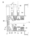
- FIG. 1 shows a schematic diagram of the inside of an electron gun 10 according to the present invention.
- the electron gun 10 has a cylindrical casing 11, and a discharge port 13 is formed at one end of the casing 11.
- a cathode electrode 21 is disposed on the bottom surface 12 opposite to the discharge port 13.
- the Wehnelt electrode 22 is disposed at a position close to and separated from the cathode electrode 21.
- the Wehnelt electrode 22 has a ring shape having a Wehnelt hole 25 that is a through hole in the center, has the same central axis 28 as the cathode electrode 21, and is arranged so that the inner surface of the Wehnelt hole 25 and the cathode side face are adjacent to each other.
- An anode electrode 23 and a repeller electrode 24 are arranged in this order from the Wehnelt electrode 22 side to the emission port 13 side of the cathode electrode 21 and the Wehnelt electrode 22.
- the anode electrode 23 has a ring shape having an anode hole 26 as a through hole in the center
- the repeller electrode 24 has a cylindrical shape with one end facing the cathode electrode 21 and the other end facing the discharge port 13.
- the central axis 28 of the electrode 24 passes through the center of the cathode electrode 21, and coincides with the central axis of the Wehnelt electrode 22 and the central axis of the anode electrode 23.
- the repeller electrode 24 has a cylindrical shape so that the electric field inside the repeller electrode 24 is axisymmetric.
- the vacuum tank vacuum pump 6 and the vacuum pumps 16 and 17 connected to the first and second vacuum exhaust ports 34 and 35 are operated to And the inside of the housing 11 are evacuated.
- a heating device 38 is disposed on the back surface of the cathode electrode 21. While the heating device 38 generates heat and the cathode electrode 21 is heated, a negative voltage with respect to the ground potential is applied to the cathode electrode 21 by the power supply device 30. The same voltage as that of the cathode electrode 21 is applied to the Wehnelt electrode 22. A positive voltage with respect to the cathode electrode 21 is applied to the anode electrode 23. Here, the anode electrode 23 is connected to the ground potential.
- a negative high voltage (for example, ⁇ 40 kV) is applied to the cathode electrode 21, and the thermoelectrons emitted from the cathode electrode 21 are focused into a beam by the Wehnelt electrode 22 and the anode electrode 23, and the anode electrode 23 , Passes through the Wehnelt hole 25 and the anode hole 26, travels along the central axis 28 of the repeller electrode 24, and passes through the repeller electrode 24.
- Reference numerals 31, 32, and 33 denote a first focusing coil, a second focusing coil, and an oscillating coil, respectively.
- the first focusing coil 31 is located outside a part of the anode electrode 23 and is a part of the anode electrode 23. Is placed around.
- the second focusing coil 32 and the oscillating coil 33 are arranged on the downstream side of the electron beam with respect to the first focusing coil 31 and in this order from the first focusing coil 31 side so as to surround the trajectory of the electron beam. Yes.
- the repeller electrode 24 is located between the first focusing coil 31 and the second focusing coil 32.
- the electron beam is focused by the first and second focusing coils 31 and 32, emitted from the emission port 13, and irradiated on the object in the vacuum chamber 18.
- the first vacuum exhaust port 34 described above is connected to an electron gun chamber that is a portion between the anode electrode 23 and the cathode electrode 21 in the space inside the housing 11, and evacuates the gas located in the electron gun chamber. Is configured to do.
- the second vacuum exhaust port 35 is a portion between the anode electrode 23 and the discharge port 13 in the space inside the housing 11 and is a portion closer to the cathode electrode 21 than the second focusing coil 32. It is connected to the chamber and is configured to evacuate the gas located in the intermediate chamber.
- the conductive plate having a large number of pores may be formed into a disc shape to form the repeller electrode 24.
- a part of the metal hollow cylinder may be slit or notched, for example, processed into a crown shape, or a repeller electrode 24 processed into a spiral shape.
- gas can pass through the pores, slits, or notches, and the passed gas is evacuated from the second vacuum exhaust port 35.
- the slit, notch, pore, or other gas passing means intersects the repeller electrode 24 perpendicularly to the central axis of the electron beam so as not to affect the trajectory of the electron beam. It is desirable to provide the gas passing means so as to be rotationally symmetric about the central axis of the electron beam when it is cut along a plane.
- the interior of the vacuum chamber 18 and the portion closer to the vacuum chamber 18 than the intermediate chamber inside the housing 11 are high-pressure spaces, and an electron beam collides with a large amount of residual gas, ionizing the residual gas and generating positive ions. .
- the generated positive ions gather on the central axis of the electron beam having a low potential, and travel toward the cathode electrode 21 having a higher negative potential.
- a positive voltage is applied to the repeller electrode 24 with respect to the anode electrode 23, and the potential of the central axis 28 of the repeller electrode 24 is higher than when there is no repeller electrode 24 to which a positive voltage is applied. Has also been raised.
- the potential on the central axis 28 of the repeller electrode 24 is maximum in the repeller electrode 24. Is applied to the repeller electrode 24.
- an electric field having a higher potential on the side of the repeller electrode 24 than the potential on the side of the discharge port 13 is formed between the discharge port 13 and the repeller electrode 24, and is closer to the discharge port 13 than in the vacuum chamber 18 or the repeller electrode 24.
- the positive ions generated in the space are pushed back by the electric field and do not enter the cathode electrode 21 side beyond the electric field formed by the repeller electrode 24.
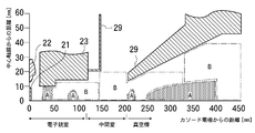
- FIG. 3 is a result of simulating the behavior of positive ions located inside the electron gun 10 when the electron beam is irradiated from the cathode electrode 21 of the electron gun having the structure of FIG.
- a range in which positive ions incident on the electrode 21 are located is indicated by being surrounded by an alternate long and short dash line with a symbol A.
- the range in which positive ions that did not reach the cathode electrode 21 even when the electron beam was irradiated was surrounded by an alternate long and short dash line with a symbol B.
- the electron gun chamber and the intermediate chamber are directly evacuated from the first and second vacuum exhaust ports 34 and 35, respectively.
- the electron gun chamber is 1 ⁇ 10 ⁇ 4 Pa or less, and the intermediate chamber is 1 ⁇ 10 ⁇ 3 Pa. In actuality, almost no positive ions are generated, and the amount of positive ions incident on the cathode electrode 21 is very small.
- the simulation conditions are: the potential of the repeller electrode 24 is +300 V, the potential of the Wehnelt electrode 22 is ⁇ 40 kV, the potential of the cathode electrode 21 is ⁇ 40 kV, the anode electrode 23 is 0 V (ground potential), and the electron beam current is 6 A.
- the initial ion velocity a random heat velocity of 1000 K was given.
- positive ions located on the emission port 13 side of the repeller electrode 24 do not move to the cathode electrode 21 side, and are generated in a large amount in the vacuum chamber 18 or in a space close to the vacuum chamber 18. Was not incident on the cathode electrode 21.
- FIG. 2 is a simulation result of the electron gun in which the repeller electrode 24 is removed from the electron gun 10 having the structure shown in FIG. 1.
- the structure is the same as that of the electron gun 10 shown in FIG. 1 except that there is no repeller electrode 24 to which a positive voltage is applied.
- It is a simulation result of the electron gun. Positive ions (range A) at a position closer to the discharge port 13 than the portion where the repeller electrode 24 is located are incident on the cathode electrode 21, and the residual gas pressure at this position is high. It was found that the cathode electrode 21 was damaged early because positive ions were incident.
- the said Example demonstrated the case where the vacuum processing apparatus of this invention was a vapor deposition apparatus, it is not limited to a vapor deposition apparatus, Other vacuum processing apparatuses are also included.
- the repeller electrode 24 has a cylindrical shape on both the inner periphery and the outer periphery. However, if the inner peripheral surface is cylindrical, the outer peripheral surface may not be cylindrical.
- the cross-sectional shape of the repeller electrode is preferably a circular shape that does not affect the trajectory of the electron beam as in the above-described embodiment. ) Or a combination of a polygon and an arc.
- a spiral repeller electrode whose inner peripheral surface can be in close contact with a cylindrical side surface is included, and a plurality of circular rings electrically connected to each other are parallel to each other and the centers are located on the same central axis.
- a repeller electrode may be configured.
- a repeller electrode may be configured by providing rod-shaped electrodes electrically connected to each other on the circumference of one circle in parallel to each other and at right angles to the cylinder.
- the repeller electrode 24 of the above-described embodiment is an example of a repeller electrode whose inner peripheral surface is positioned on the same cylindrical side surface.
- the inner peripheral surface may be a frustoconical repeller electrode in which one opening is wider than the other opening.
Landscapes
- Chemical & Material Sciences (AREA)
- Materials Engineering (AREA)
- Health & Medical Sciences (AREA)
- Toxicology (AREA)
- Chemical Kinetics & Catalysis (AREA)
- Engineering & Computer Science (AREA)
- Analytical Chemistry (AREA)
- Mechanical Engineering (AREA)
- Metallurgy (AREA)
- Organic Chemistry (AREA)
- Electron Sources, Ion Sources (AREA)
- Physical Vapour Deposition (AREA)
- Physical Or Chemical Processes And Apparatus (AREA)
Abstract
Description
このような電子ビームが電子銃の内部や真空槽の内部を進行する際に、残留ガスと衝突し、正に帯電したイオンを発生させる。
その正イオンは、電子ビームの空間電荷に引き寄せられ、電子ビームの中心軸線上に集まり、さらに電位の低いカソード電極に向かって中心軸線に沿って逆進する。
真空槽内や電子放出口付近で発生した正イオンは最終的にカソード電極に引き付けられて加速され、カソード電極に衝突してしまう。
この衝突によるイオン衝撃によってカソード電極は損傷を蒙り、電子放出面の後退、変形、甚だしい場合には中心部に穿孔が生じ、カソード電極の寿命を縮める主要な原因となっている。また、イオンの衝突によってカソード電極がスパッタされ、飛散したカソード電極材料は主にアノード電極に付着して、これがアノード電極の温度変化などにより剥がれるなどして異常放電の原因にもなっている。
本発明は、前記カソード電極と前記ウェーネルト電極と前記アノード電極と前記リペラー電極が配置された筺体を有し、前記筺体には、前記筺体内の空間のうち、前記アノード電極と前記カソード電極との間の部分を真空排気する第一の真空排気口と、前記アノード電極と前記放出口の間の部分を真空排気する第二の真空排気口とが設けられた電子銃である。
本発明は、前記リペラー電極には細孔が形成され、前記リペラー電極で囲まれた空間に位置するガスは、前記細孔を通過して前記第二の真空排気口から真空排気される電子銃である。
本発明は、前記リペラー電極は網状の導電材料によって円筒形形状に成形された電子銃である。
本発明は、前記リペラー電極は、内周面が同一の筒形状の側面に位置するようにされた電子銃である。
本発明は、真空槽と、上記いずれかの電子銃とを有し、前記真空槽の内部と前記電子銃の内部が接続され、前記真空槽内に前記放出口から放出された前記電子ビームが照射される照射対象物が配置された真空処理装置である。
リペラー電極には、アノード電極に対して正電圧が印加され、放出口側からリペラー電極に向かって飛来する正イオンを放出口側に押し戻すように構成されている。
また、リペラー電極には細孔を形成し、細孔を介してリペラー電極で取り囲んだ空間を真空排気できるようにしたから、リペラー電極を設けても中間室の排気を妨げない。
3:基板
4:蒸着材料
5:基板ホルダ
6:真空槽用真空ポンプ
10:電子銃
11:筺体
12:底面
13:放出口
16、17:真空ポンプ
18:真空槽
21:カソード電極
22:ウェーネルト電極
23:アノード電極
24:リペラー電極
25:ウェーネルト孔
26:アノード孔
28:中心軸線
31:第一集束コイル
32:第二集束コイル
33:揺動コイル
34:第一の真空排気口
35:第二の真空排気口
真空槽18には、真空槽用真空ポンプ6が接続されており、この真空槽用真空ポンプ6によって真空槽18内部を真空排気し、真空雰囲気を維持しながら真空槽18内に基板3を搬入し、基板ホルダ5に保持させる。
真空槽18の壁面や天井に、本発明の電子銃10が取り付けられており、電子銃10内を直接真空排気して、電子銃10内を真空槽18内よりも高真空雰囲気にしながら、電子銃10から電子ビームを真空槽18内に放出させ、蒸着材料4に照射すると、真空雰囲気中で蒸着材料4が蒸発し、その蒸気が基板3に到達して基板3表面に蒸着材料4の薄膜が形成される。
この電子銃10は、筒状の筺体11を有しており、筺体11の一端部には放出口13が形成されている。放出口13とは反対側の底面12の上には、カソード電極21が配置されている。また、カソード電極21と近接して離間した位置にウェーネルト電極22が配置されている。
ウェーネルト電極22は、中央に貫通孔であるウェーネルト孔25を有するリング形状であり、カソード電極21と同じ中心軸線28を持ち、ウェーネルト孔25の内面とカソード側面が隣合うように配置する。
カソード電極21とウェーネルト電極22よりも放出口13側には、ウェーネルト電極22側からアノード電極23とリペラー電極24とがこの順序で配置されている。
アノード電極23は、中央に、貫通孔であるアノード孔26を有するリング形状であり、リペラー電極24は、一端をカソード電極21側と他端を放出口13側に向けた筒形状であり、リペラー電極24の中心軸線28は、カソード電極21の中心を通っており、また、ウェーネルト電極22の中心軸線とアノード電極23の中心軸線と一致するようにされている。ここでは、リペラー電極24は、リペラー電極24内部の電界が軸対称になるように、円筒形状である。
筺体11及び真空槽18の外部には電源装置30が配置されており、各電極21~24は電源装置30に接続されている。
筺体11には、第一、第二の真空排気口34、35が設けられており、第一、第二の真空排気口34、35は、真空ポンプ16、17に接続されている。ここでは、第一、第二の真空排気口34、35は、それぞれ別の真空ポンプ16、17に接続されている。
カソード電極21の裏面には、加熱装置38が配置されており、加熱装置38を発熱させ、カソード電極21を加熱しながら、電源装置30によって、カソード電極21には接地電位に対する負電圧を印加し、ウェーネルト電極22にはカソード電極21と同電圧を印加する。アノード電極23にはカソード電極21に対する正電圧を印加する。ここではアノード電極23は接地電位に接続されている。
電源装置30により、リペラー電極24にはアノード電極23に対する正電圧が印加されているが、ビームの中心軸はリペラー電極24の中心軸線28と一致しているのでビームの軸対称性が崩れることはない。
各電極21~24の電位を比較すると、ウェーネルト電極=カソード電極<アノード電極<リペラー電極 の順にされており、ここではアノード電極23は接地電位に接続されている。
第二集束コイル32と揺動コイル33は、第一集束コイル31よりも電子ビームの下流側であって、第一集束コイル31側からこの順序で、電子ビームの軌道を取り囲むように配置されている。リペラー電極24は、第一集束コイル31と第二集束コイル32の間に位置している。
電子ビームは第一、第二集束コイル31、32によって集束されて放出口13から放出され、真空槽18内の対象物に照射される。
この図4及び後述する図2、3は、電子銃10及びリペラー電極24の中心軸線28の排気口が位置する片側だけが示されている。
なお、揺動コイル33を動作させると放出口13から放出される電子ビームは進行方向が揺動され、対象物には、電子ビームの断面積よりも大きい範囲に照射することができる。
また、第二の真空排気口35は、筺体11内部の空間のうち、アノード電極23と放出口13の間の部分であって、第二集束コイル32よりもカソード電極21に近い部分である中間室に接続され、中間室内に位置するガスを真空排気するように構成されている。
リペラー電極24は、図5(b)に示すように、金属製の網41から構成されており、中間室に位置するガスは、網41の目42を通過して、第二の真空排気口35から真空排気される。
なお、上述した実施例では、金属製の網としたが、複数本の金属製の細い棒で同じ円筒の側面に位置するように、電子ビームの進行方向と平行に等間隔に配置して、筒状形状のリペラー電極24を構成してもよい。また、細孔が多数形成された導電性の板を円板状に成形してリペラー電極24にしてもよい。また、金属製の中空円筒の一部をスリット加工や切り欠き加工、例えば、王冠形状に加工し、または、螺旋形状に加工したリペラー電極24にしてもよい。
これらリペラー電極24では、細孔、スリット、又は切り欠きをガスが通過でき、通過したガスが第二の真空排気口35から真空排気される。
いずれのリペラー電極4の場合でも、スリット、切り欠き、細孔、又はその他のガス通過手段では、電子ビームの軌道に影響を及ぼさないように、リペラー電極24を電子ビームの中心軸線と垂直に交わる平面で截断したときに、ガス通過手段は電子ビームの中心軸線を中心として回転対称となるように設けることが望ましい。
電子銃10の筺体11の内部では、第一、第二の真空排気口34、35からの真空排気によって、電子銃室の圧力が中間室の圧力よりも低くなっており、中間室の圧力は、中間室よりも真空槽18に近い部分の圧力よりも低くなっている。
真空槽18の内部や、筺体11内部の中間室よりも真空槽18に近い部分は圧力の高い空間であり、多い残留気体に電子ビームが衝突し、残留気体が電離して正イオンが発生する。
発生した正イオンは、電位が低い電子ビームの中心軸線に集まり、更に負電位が大きいカソード電極21側に向かって進行する。
特に、本発明では、カソード電極21から放出された電子ビームがリペラー電極24の中心軸線28上を進行しているときでも、リペラー電極24の中心軸線28上の電位が、リペラー電極24内部で最大になる電圧がリペラー電極24に印加されている。
また、電子ビームを照射してもカソード電極21に到達しなかった正イオンが位置していた範囲を、符号Bを付した一点鎖線で囲んで示した。
電子銃室と中間室は、第一、第二の真空排気口34、35からそれぞれ直接真空排気されており、電子銃室は1×10⁻⁴Pa以下、中間室は1×10⁻³Pa以下の圧力にされており、実際には正イオンはほとんど発生せず、カソード電極21に入射する正イオンは微少である。
その条件では、リペラー電極24よりも放出口13側に位置していた正イオンは、カソード電極21側に移動せず、真空槽18内や、真空槽18に近い空間で多量に発生した正イオンは、カソード電極21には入射しないことが分かった。
リペラー電極24が位置する部分よりも放出口13に近い位置の正イオン(符号Aの範囲)がカソード電極21に入射しており、この位置の残留ガスの圧力は高いために、大量に発生した正イオンが入射するから、カソード電極21が早く損傷することが分かった。
なお、上記実施例では、本発明の真空処理装置が蒸着装置の場合を説明したが、蒸着装置に限定されるものではなく、他の真空処理装置も含まれる。
また、上記実施例では、リペラー電極24は内周も外周も円筒状であったが、内周面が円筒状であれば、外周面が円筒でなくてもよい。
リペラー電極の断面形状は、上記実施例のように、電子ビームの軌道に影響を及ぼさない円形が望ましいが、装置構成上の制約や製造コストの都合により、ルーローの三角形やペリトロコイド曲線(繭型)といった多角形と円弧を組み合わせた形状でも良い。
また、内周面が円筒形状の側面と密着できる螺旋形状のリペラー電極も含まれるし、互いに電気的に接続された複数の円形リングを、互いに平行に、中心が同一の中心軸線上に位置するようにしてリペラー電極を構成してもよい。
また、互いに電気的に接続された棒状の電極を、一つの円の円周上に、互いに平行に、円柱とは直角に、設けてリペラー電極を構成してもよい。
要するに、上記実施例のリペラー電極24は、内周面が同一の筒形状の側面に位置するようにされたリペラー電極の一例である。
また、円筒に限らず、内周面が一方の開口が他方の開口よりも広がった円錐台形状のリペラー電極であってもよい。
Claims (6)
- 加熱されて熱電子を放出するカソード電極と、
前記カソード電極から放出された電子ビームを集束するウェーネルト電極と、
アノード孔を有し、前記カソード電極に対して正電圧が印加され、前記熱電子が電子ビームとして前記アノード孔を通過するアノード電極と、
前記アノード電極に対して正電圧が印加され、
前記アノード電極と前記電子ビームが放出される放出口の間に設けられ、前記電子ビームを中心軸線に沿って通過させるリペラー電極と、
前記リペラー電極を通過した前記電子ビームが放出される放出口とを有する電子銃。 - 前記カソード電極と前記ウェーネルト電極と前記アノード電極と前記リペラー電極が配置された筺体を有し、
前記筺体には、前記筺体内の空間のうち、前記アノード電極と前記カソード電極との間の部分を真空排気する第一の真空排気口と、前記アノード電極と前記放出口の間の部分を真空排気する第二の真空排気口とが設けられた請求項1記載の電子銃。 - 前記リペラー電極には細孔が形成され、
前記リペラー電極で囲まれた空間に位置するガスは、前記細孔を通過して前記第二の真空排気口から真空排気される請求項1又は請求項2のいずれか1項記載の電子銃。 - 前記リペラー電極は網状の導電材料によって円筒形形状に成形された請求項3記載の電子銃。
- 前記リペラー電極は、内周面が同一の筒形状の側面に位置するようにされた請求項3記載の電子銃。
- 真空槽と、
請求項1乃至請求項5のいずれか1項記載の電子銃とを有し、
前記真空槽の内部と前記電子銃の内部が接続され、
前記真空槽内に前記放出口から放出された前記電子ビームが照射される照射対象物が配置された真空処理装置。
Priority Applications (2)
| Application Number | Priority Date | Filing Date | Title |
|---|---|---|---|
| CN201080041421.9A CN102484024B (zh) | 2009-09-18 | 2010-09-15 | 电子枪、真空处理装置 |
| JP2011531943A JP5186599B2 (ja) | 2009-09-18 | 2010-09-15 | 電子銃、真空処理装置 |
Applications Claiming Priority (2)
| Application Number | Priority Date | Filing Date | Title |
|---|---|---|---|
| JP2009216506 | 2009-09-18 | ||
| JP2009-216506 | 2009-09-18 |
Publications (1)
| Publication Number | Publication Date |
|---|---|
| WO2011034086A1 true WO2011034086A1 (ja) | 2011-03-24 |
Family
ID=43758687
Family Applications (1)
| Application Number | Title | Priority Date | Filing Date |
|---|---|---|---|
| PCT/JP2010/065931 Ceased WO2011034086A1 (ja) | 2009-09-18 | 2010-09-15 | 電子銃、真空処理装置 |
Country Status (4)
| Country | Link |
|---|---|
| JP (1) | JP5186599B2 (ja) |
| CN (1) | CN102484024B (ja) |
| TW (1) | TWI476805B (ja) |
| WO (1) | WO2011034086A1 (ja) |
Cited By (4)
| Publication number | Priority date | Publication date | Assignee | Title |
|---|---|---|---|---|
| JP2019050141A (ja) * | 2017-09-11 | 2019-03-28 | 株式会社ニューフレアテクノロジー | 荷電粒子装置、荷電粒子描画装置および荷電粒子ビーム制御方法 |
| WO2020079929A1 (ja) | 2018-10-16 | 2020-04-23 | 株式会社Photo electron Soul | 電子銃、電子線適用装置、電子銃による電子射出方法、および、電子ビームの焦点位置調整方法 |
| EP3806130A2 (en) | 2019-10-07 | 2021-04-14 | Jeol Ltd. | Electron gun and method of adjusting current of electron gun |
| CN115335948A (zh) * | 2020-04-13 | 2022-11-11 | 浜松光子学株式会社 | 电子束产生器及x射线产生装置 |
Families Citing this family (4)
| Publication number | Priority date | Publication date | Assignee | Title |
|---|---|---|---|---|
| CN110196362B (zh) * | 2019-05-05 | 2022-10-04 | 中国科学院电子学研究所 | 电子枪发射性能的测试系统及方法 |
| JP7269107B2 (ja) * | 2019-06-12 | 2023-05-08 | 日清紡マイクロデバイス株式会社 | 電子銃 |
| JP6762635B1 (ja) * | 2020-04-16 | 2020-09-30 | 株式会社Photo electron Soul | 電子銃、電子線適用装置、および、電子ビームの射出方法 |
| JP7573457B2 (ja) * | 2021-02-25 | 2024-10-25 | 株式会社ニューフレアテクノロジー | 電子銃の陰極機構、電子銃、及び電子ビーム描画装置 |
Citations (4)
| Publication number | Priority date | Publication date | Assignee | Title |
|---|---|---|---|---|
| JPS5784655U (ja) * | 1980-11-14 | 1982-05-25 | ||
| JPS6386339A (ja) * | 1986-09-29 | 1988-04-16 | イメイトロン インコ−ポレ−テツド | イオン除去電極 |
| JPH077648B2 (ja) * | 1986-11-22 | 1995-01-30 | 日本真空技術株式会社 | 空間電荷中和型電子銃 |
| JPH07249391A (ja) * | 1994-03-09 | 1995-09-26 | Fujitsu Ltd | 電子ビーム装置 |
Family Cites Families (5)
| Publication number | Priority date | Publication date | Assignee | Title |
|---|---|---|---|---|
| CN1021390C (zh) * | 1985-04-01 | 1993-06-23 | 株式会社岛津制作所 | 分析用辉光放电管 |
| JPH07249383A (ja) * | 1994-03-08 | 1995-09-26 | Hitachi Ltd | 電子銃とその組立て方法 |
| EP0782174A1 (en) * | 1995-12-26 | 1997-07-02 | Nihon Shinku Gijutsu Kabushiki Kaisha | Sputter ion pump |
| JP2001176422A (ja) * | 1999-12-17 | 2001-06-29 | Hitachi Ltd | カラ−陰極線管 |
| JP2007066694A (ja) * | 2005-08-31 | 2007-03-15 | Hamamatsu Photonics Kk | X線管 |
-
2010
- 2010-09-15 CN CN201080041421.9A patent/CN102484024B/zh active Active
- 2010-09-15 WO PCT/JP2010/065931 patent/WO2011034086A1/ja not_active Ceased
- 2010-09-15 JP JP2011531943A patent/JP5186599B2/ja active Active
- 2010-09-16 TW TW099131461A patent/TWI476805B/zh active
Patent Citations (4)
| Publication number | Priority date | Publication date | Assignee | Title |
|---|---|---|---|---|
| JPS5784655U (ja) * | 1980-11-14 | 1982-05-25 | ||
| JPS6386339A (ja) * | 1986-09-29 | 1988-04-16 | イメイトロン インコ−ポレ−テツド | イオン除去電極 |
| JPH077648B2 (ja) * | 1986-11-22 | 1995-01-30 | 日本真空技術株式会社 | 空間電荷中和型電子銃 |
| JPH07249391A (ja) * | 1994-03-09 | 1995-09-26 | Fujitsu Ltd | 電子ビーム装置 |
Cited By (5)
| Publication number | Priority date | Publication date | Assignee | Title |
|---|---|---|---|---|
| JP2019050141A (ja) * | 2017-09-11 | 2019-03-28 | 株式会社ニューフレアテクノロジー | 荷電粒子装置、荷電粒子描画装置および荷電粒子ビーム制御方法 |
| WO2020079929A1 (ja) | 2018-10-16 | 2020-04-23 | 株式会社Photo electron Soul | 電子銃、電子線適用装置、電子銃による電子射出方法、および、電子ビームの焦点位置調整方法 |
| KR20200130420A (ko) | 2018-10-16 | 2020-11-18 | 가부시키가이샤 포토 일렉트론 소울 | 전자 총, 전자선 적용 장치, 전자 총에 의한 전자 사출 방법, 및, 전자 빔의 초점 위치 조정 방법 |
| EP3806130A2 (en) | 2019-10-07 | 2021-04-14 | Jeol Ltd. | Electron gun and method of adjusting current of electron gun |
| CN115335948A (zh) * | 2020-04-13 | 2022-11-11 | 浜松光子学株式会社 | 电子束产生器及x射线产生装置 |
Also Published As
| Publication number | Publication date |
|---|---|
| JPWO2011034086A1 (ja) | 2013-02-14 |
| TWI476805B (zh) | 2015-03-11 |
| TW201130008A (en) | 2011-09-01 |
| CN102484024B (zh) | 2015-08-12 |
| JP5186599B2 (ja) | 2013-04-17 |
| CN102484024A (zh) | 2012-05-30 |
Similar Documents
| Publication | Publication Date | Title |
|---|---|---|
| JP5186599B2 (ja) | 電子銃、真空処理装置 | |
| CN101156505B (zh) | 用于生成、加速和传播电子束和等离子体束的设备和方法 | |
| JP5822767B2 (ja) | イオン源装置及びイオンビーム生成方法 | |
| EP2492949B1 (en) | Stable cold field emission electron source | |
| JP2008518407A5 (ja) | ||
| RU2014109915A (ru) | Осаждение из паровой фазы для нанесения покрытия с погружением в дуговую плазму низкого давления и ионная обработка | |
| AU2003235984A1 (en) | Gas discharge tube | |
| JP5370967B2 (ja) | X線管 | |
| US3517240A (en) | Method and apparatus for forming a focused monoenergetic ion beam | |
| TWI730553B (zh) | 電子槍、x射線產生裝置及x射線攝像裝置 | |
| US4004172A (en) | Gas discharge electron gun for generating an electron beam by means of a glow discharge | |
| JP6194178B2 (ja) | 電子銃及び電子ビームの放出方法 | |
| RU107657U1 (ru) | Форвакуумный плазменный электронный источник | |
| RU2654494C1 (ru) | Вакуумный искровой разрядник | |
| RU209138U1 (ru) | Форвакуумный плазменный источник импульсного электронного пучка на основе контрагированного дугового разряда | |
| JPH11232995A (ja) | 電子管の動作方法 | |
| US2956192A (en) | Gettering electron gun | |
| JP2010248574A (ja) | 蒸着装置及び蒸着方法。 | |
| RU2313848C1 (ru) | Сильноточная электронная пушка | |
| US3328628A (en) | Electron tube employing a relatively long electron beam and getter material disposedat the collector | |
| RU2306683C1 (ru) | Плазменный электронный источник | |
| JPH07254388A (ja) | スパッタイオンポンプ | |
| Denbnovetsky et al. | High voltage glow discharge electron sources and possibilities of its technological application | |
| US20250188592A1 (en) | High-efficiency target for an ion source | |
| RU2654493C1 (ru) | Вакуумный разрядник |
Legal Events
| Date | Code | Title | Description |
|---|---|---|---|
| WWE | Wipo information: entry into national phase |
Ref document number: 201080041421.9 Country of ref document: CN |
|
| 121 | Ep: the epo has been informed by wipo that ep was designated in this application |
Ref document number: 10817199 Country of ref document: EP Kind code of ref document: A1 |
|
| WWE | Wipo information: entry into national phase |
Ref document number: 2011531943 Country of ref document: JP |
|
| NENP | Non-entry into the national phase |
Ref country code: DE |
|
| 122 | Ep: pct application non-entry in european phase |
Ref document number: 10817199 Country of ref document: EP Kind code of ref document: A1 |