WO2011033941A1 - 微細パターン形成方法 - Google Patents
微細パターン形成方法 Download PDFInfo
- Publication number
- WO2011033941A1 WO2011033941A1 PCT/JP2010/065036 JP2010065036W WO2011033941A1 WO 2011033941 A1 WO2011033941 A1 WO 2011033941A1 JP 2010065036 W JP2010065036 W JP 2010065036W WO 2011033941 A1 WO2011033941 A1 WO 2011033941A1
- Authority
- WO
- WIPO (PCT)
- Prior art keywords
- mold
- film
- fine pattern
- glass substrate
- forming
- Prior art date
- Legal status (The legal status is an assumption and is not a legal conclusion. Google has not performed a legal analysis and makes no representation as to the accuracy of the status listed.)
- Ceased
Links
Images



Classifications
-
- C—CHEMISTRY; METALLURGY
- C03—GLASS; MINERAL OR SLAG WOOL
- C03C—CHEMICAL COMPOSITION OF GLASSES, GLAZES OR VITREOUS ENAMELS; SURFACE TREATMENT OF GLASS; SURFACE TREATMENT OF FIBRES OR FILAMENTS MADE FROM GLASS, MINERALS OR SLAGS; JOINING GLASS TO GLASS OR OTHER MATERIALS
- C03C17/00—Surface treatment of glass, not in the form of fibres or filaments, by coating
- C03C17/34—Surface treatment of glass, not in the form of fibres or filaments, by coating with at least two coatings having different compositions
- C03C17/36—Surface treatment of glass, not in the form of fibres or filaments, by coating with at least two coatings having different compositions at least one coating being a metal
- C03C17/40—Surface treatment of glass, not in the form of fibres or filaments, by coating with at least two coatings having different compositions at least one coating being a metal all coatings being metal coatings
-
- C—CHEMISTRY; METALLURGY
- C03—GLASS; MINERAL OR SLAG WOOL
- C03C—CHEMICAL COMPOSITION OF GLASSES, GLAZES OR VITREOUS ENAMELS; SURFACE TREATMENT OF GLASS; SURFACE TREATMENT OF FIBRES OR FILAMENTS MADE FROM GLASS, MINERALS OR SLAGS; JOINING GLASS TO GLASS OR OTHER MATERIALS
- C03C2217/00—Coatings on glass
- C03C2217/70—Properties of coatings
- C03C2217/77—Coatings having a rough surface
Definitions
- the present invention relates to a method for producing a nanometer-sized fine film pattern on a large-area substrate at low cost.
- a photolithography method has been widely used as a fine pattern forming method.
- expensive exposure equipment and peripheral equipment are required, and their application is highly functional from the viewpoint of processing costs.
- high value-added products such as semiconductors.
- the nanoimprint method has attracted attention as a method for producing a nanometer-sized fine pattern with a simple apparatus.
- the nanoimprint method is a method of transferring the shape of a mold serving as an original plate to a resin or the like using heating and pressing.
- the nanoimprint method has an advantage that a fine shape can be produced in a single process, and can produce nanostructures at low cost (see Patent Documents 1 to 3 and Non-Patent Documents 1 and 2).
- a nano-transfer method is known as a technique for forming a fine film material pattern using a mold (see Patent Document 3, Non-Patent Documents 1 and 2).
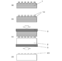
- a film material 10 is formed on the surface of the mold 1 as shown in FIGS. 2A to 2D, and this and the substrate 2 are mechanically pressurized under heating (see heater 3).
- the film material of the mold convex part is bonded on the substrate. Thereafter, the film material is peeled from the mold to form a fine film pattern 20 on the substrate 2.
- the nanotransfer method it is possible to form a fine film pattern by a simple process, but since it is necessary to perform bonding by heating and pressurization, a resin or glass substrate that softens by heating is used, It is necessary to coat an adhesive layer for improving the bonding property on the substrate.
- a resin or glass substrate When a resin or glass substrate is used, the substrate itself may be deformed in the heating and pressing process for bonding, so the heating temperature and pressure are limited, affecting the bonding strength between the substrate and the membrane material. To do.
- the fine pattern forming method of the present invention comprises a step of forming a film material on the surface of a mold having irregularities on the surface, and a mold on which the film material is formed and glass are brought into contact with each other under heating. And applying a voltage to generate a uniform electrostatic attraction between the mold surface and the glass substrate surface, and bonding the film material formed on the mold convex portion on the glass substrate as a film pattern; After the application is completed, the method includes a step of peeling the mold and the glass substrate and transferring the film pattern onto the glass substrate.
- the fine pattern forming method of the present invention is further characterized in that the glass substrate is a glass material containing an alkali metal.
- the fine pattern forming method of the present invention is further characterized in that the film material is a multilayer film composed of two or more layers.
- the fine pattern forming method of the present invention is further characterized in that the lowermost layer of the multilayer film is gold.
- the fine pattern forming method of the present invention is further characterized in that the uppermost layer of the multilayer film is aluminum or silicon.
- the fine pattern forming method of the present invention is further characterized in that the mold is made of a conductive material.
- the fine pattern forming method of the present invention is further characterized in that the mold is made of silicon.
- the fine pattern forming method of the present invention is further characterized in that a silicon oxide film is formed on the surface of the silicon mold.
- the fine pattern forming method of the present invention is further characterized in that the applied voltage is a DC voltage with the mold being positive and the glass substrate being negative.
- the fine pattern forming method of the present invention is further characterized in that the applied voltage varies in polarity between positive and negative with respect to time.
- the fine pattern forming method of the present invention is further characterized in that when the polarity of the applied voltage is time-averaged, the time for making the mold positive is longer than the time for making the mold negative.
- the fine pattern forming method of the present invention is further characterized in that the applied voltage when the mold is positive is higher than the applied voltage when the mold is negative.
- the fine pattern forming method of the present invention is further characterized in that the step of applying a voltage under heating is performed in a vacuum or in a nitrogen gas atmosphere or an argon gas atmosphere.
- the fine pattern forming method of the present invention is further characterized in that at least one of the film materials is formed by a vacuum deposition method.
- a film material is formed on the surface of a mold having irregularities on the surface, a voltage is applied under heating by bringing the mold into contact with the glass substrate, and the thin film formed on the convex portion of the mold is bonded to the glass substrate.
- the cations 31 in the glass substrate 30 move as shown in FIG. 3, and negative charges 32 accumulate on the glass surface. Due to the mirror image force with respect to the negative charge, the positive charge 33 is accumulated on the surface of the mold or the film material. Therefore, the mold and the glass substrate 30 are brought into close contact with each other by the electrostatic attractive force acting between these positive and negative charges.
- the film pattern can be firmly bonded to the glass substrate surface at a temperature lower than the softening temperature of the glass, so that the substrate is hardly deformed.
- glass and a film material can be directly bonded without using an intermediate material such as a resin, a product excellent in heat resistance and chemical stability can be manufactured.
- a large force due to electrostatic force can be uniformly applied between the mold and the glass substrate by applying a voltage.
- the manufacturing apparatus can be simplified.
- the mechanical load increases in proportion to the substrate area, but the electrostatic force due to voltage application is proportional only to the voltage regardless of the area, so that a film pattern having a large area can be formed with the same voltage.
- the electrostatic force acts uniformly over the entire contact surface between the mold and the glass substrate, a uniform film pattern can be formed even in a large area.
- the pattern size that can be formed depends only on the pattern of the mold, the pattern size is not limited in principle, and a very fine film pattern on the nanometer scale can be created. Is possible.
- the mold after transferring the film can be easily reused by washing with an acid or the like. From this, it can be said that it is very advantageous for forming a fine pattern as compared with the conventional photolithography method in which the pattern size is limited by the wavelength of light.
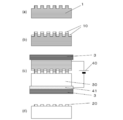
- FIGS. 1A to 1D are process diagrams showing the fine pattern forming method of the present invention.
- a mold 1 having an uneven surface as shown in FIG. 1A is used, and a film material 10 is formed on the surface of the mold 1 (see FIG. 1B).
- the film material 10 is formed in the convex portion and the concave portion, and hardly formed in the rising portion of the concave and convex portions.
- a voltage is applied between the mold 1 and the substrate glass 30 from the power source 40 via the glass substrate side electrode 41 under heating by bringing the mold 1 and the glass substrate 30 into contact with each other, and a film material formed on the convex portion of the mold is obtained.
- the film pattern 20 is bonded to a glass substrate (see FIG. 1C).
- the heater 3 is used as a heating means, other heating means, such as a heating medium, can also be used.
- the cations (M + ) 31 in the glass move as shown in FIG. 3, and negative charges ( ⁇ ) 32 accumulate on the glass substrate surface.
- the glass substrate is preferably a glass material containing an alkali metal. Since the alkali metal easily moves in the glass by an electric field, more electric charges are accumulated on the glass surface, a large electrostatic attraction is obtained, and the bonding strength of the film pattern is improved.
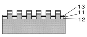
- the film material formed on the surface of the mold 1 is preferably a multilayer film composed of two or more layers.
- FIG. 4 shows an example in which the film material is composed of three layers.
- the lowermost layer 12 can be made of a material that can be easily peeled off from the mold after bonding, and the uppermost layer 13 is made of a material that forms a strong bond with the glass substrate.
- the film pattern can be firmly fixed to the substrate.
- various functional materials in the intermediate layer it becomes possible to produce fine patterns having various functions.
- the lowermost layer of the multilayer film is preferably gold.
- the uppermost layer of the multilayer film is preferably aluminum or silicon. Since aluminum and silicon are firmly bonded to the glass substrate by applying a voltage under heating, the bonding strength of the film pattern to the substrate can be improved. Further, it is desirable that at least one of the layers forming the film material is formed by a vacuum deposition method. In the vacuum deposition method, since there is less reaction with the base material than in other film forming methods, the mold and the film material after bonding can be easily separated.
- the mold is preferably made of a conductive material.
- the conductive material constituting the mold is preferably made of silicon. Silicon has developed many microfabrication methods necessary for mold production, and it is easy to form a fine pattern as compared with other materials, and mold production at a low cost is possible. It is desirable that a silicon oxide film be formed on the surface of the silicon mold. The silicon oxide film is chemically stable and can suppress the deterioration of the shape of the mold associated with the application of voltage under heating. Further, the reaction between the film material and silicon is suppressed, and the film pattern can be easily peeled off from the mold after bonding to the glass substrate.
- the voltage applied between the mold and the glass substrate is preferably a DC voltage with the mold being positive and the glass substrate being negative.
- the voltage applied between the mold and the glass substrate is set to this polarity, the charge accumulation at the contact portion is maximized, and the maximum electrostatic attraction is obtained.
- the polarity of the applied voltage is time-averaged, it is desirable that the time for making the mold positive is longer than the time for making the mold negative.
- the electric charge accumulate
- the positive and negative polarities change with respect to time when the voltage applied between the mold and the glass substrate changes, the applied voltage when the mold is positive is higher than the applied voltage when the mold is negative Is desirable.
- the electric charge accumulate
- the step of applying a voltage under heating is preferably performed in a vacuum or in a nitrogen gas atmosphere or an argon gas atmosphere. Thereby, the oxidation of the film material during heating is suppressed, and a stronger bond is formed during voltage application.
- FIG. 5 shows a first embodiment of the present invention.
- a fine pattern having a height of 1 ⁇ m is formed on the surface of a silicon wafer having a diameter of 100 mm by a photolithography method.
- a silicon oxide film having a thickness of 0.1 ⁇ m was formed on the surface of the silicon mold 5 by a thermal oxidation method.
- a gold film 15 having a thickness of 0.1 ⁇ m was formed on the surface of the silicon mold by a vacuum vapor deposition method, and then an uppermost layer film 13 having a thickness of 0.1 to 0.2 ⁇ m was formed.
- the silicon mold 5 on which the gold film and the uppermost layer film were formed was overlaid on the silicon wafer electrode 42 and the glass substrate 30 and fixed by applying a load of about 1 N.
- a positive electrode was connected to the silicon mold 5 and a negative electrode was connected to the silicon wafer electrode 42, and a DC voltage was applied under heating in a nitrogen gas atmosphere (see FIG. 5A).
- the mold and the glass substrate were peeled off to form a multilayer film pattern 21 on the glass substrate (see FIG. 5B).
- Pyrex glass manufactured by Asahi Techno Glass
- aluminum is used for the uppermost film 13 of the multilayer film
- the heating temperature is 280 ° C.
- FIG. 6 is a photograph (before transfer (a), after transfer (b)) of a 4-inch Pyrex glass wafer 35 as a glass substrate before and after transfer of the film pattern, and on the entire surface of the 4-inch Pyrex glass wafer 35 according to the present invention, Transfer of the two-layer film pattern 22 of gold and aluminum was possible.
- FIG. 7 shows the transferred two-layer film pattern 22 of gold and aluminum observed with a scanning electron microscope.
- a fine pattern of 0.5 ⁇ m or less is transferred.
- the silicon mold 5 was cleaned by ultrasonic cleaning and a mixed solution of sulfuric acid and hydrogen peroxide after peeling. As a result, the multilayer film remaining in the recesses was removed and could be used repeatedly as a mold.
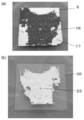
- FIG. 8 is a photograph of the mold 6 (see FIG.
- reference numeral 16 denotes a portion after the multilayer film is normally transferred to the Pyrex glass side as a film pattern
- reference numeral 17 denotes a mold 6 in which the multilayer film cannot be normally transferred to the Pyrex glass side as a film pattern
- the reference numeral 23 in FIG. 8B is a portion of a two-layer film pattern of gold and aluminum that is normally transferred as a film pattern on the Pyrex glass piece 36.
- Example 1 in which a silicon wafer having a diameter of 100 mm is used as it is as mold 5
- Comparative Example 1 a small area of 20 ⁇ 20 mm 2 was cut out from a silicon wafer having a diameter of 100 mm and used as mold 6.
- a film pattern can be formed on glass at a lower temperature than in the conventional nanotransfer method.
- crown glass (B270 manufactured by Schott Co.) is used as the glass substrate 30, gold is formed as the lowermost layer film, and aluminum is formed as the uppermost layer film in the same manner as in the first embodiment.
- the film pattern was transferred to the surface. With crown glass, film transfer was possible at 240 ° C. or higher and 400 ° C. or lower.
- Example 3 In the third embodiment of the present invention, Pyrex glass was used as the glass substrate 30, gold was formed on the mold surface as a lowermost layer film by a vacuum deposition method, and silicon was formed as an uppermost layer film by a sputtering method. The film pattern was transferred in the same manner as in Example 1. When the uppermost layer was silicon, the film could be transferred at a heating temperature of 320 ° C. or higher and 450 ° C. or lower.
- the process conditions necessary for the film pattern transfer differ depending on the glass substrate and the uppermost film material.
- the present invention is characterized in that a voltage is applied during transfer of the film, and the heating temperature, applied voltage, application time, applied pressure during transfer, and the like used in the above embodiments are examples thereof. It does not limit the conditions.
- a nanometer-sized fine pattern can be formed on a large-area substrate at low cost.
- These fine patterns are applied as manufacturing of microelectronic devices using glass substrates such as semiconductors, MEMS, display devices, and wiring boards, and in the field of their integrated mounting, to reduce manufacturing costs and increase functionality.
- a substrate other than a glass substrate can be used as long as it is made of a material that generates an electrostatic attractive force between the substrate surface and the mold surface by applying a voltage to the substrate and the mold.
- Type 1 2 substrate 3 heater 5 of silicon type 6 was cut out from the wafer 20 ⁇ 20 mm 2 silicon-type 10 film material 11 multilayer film 12 multilayer lowermost 13 uppermost 15 gold film 16 multilayer film of the multilayer film of the glass Transferred portion 17 Non-transferred multilayer film 20 Film pattern 21 Transferred multilayer film pattern 22 Double-layer film pattern 23 of gold and aluminum transferred to Pyrex glass wafer Two of gold and aluminum transferred to Pyrex glass piece Layer film pattern 30 Glass substrate 31 Cation 32 Negative charge 33 Positive charge 35 Pyrex glass wafer 36 Pyrex glass piece 40 Power supply 41 Electrode 42 Silicon wafer electrode
Landscapes
- Chemical & Material Sciences (AREA)
- Life Sciences & Earth Sciences (AREA)
- Engineering & Computer Science (AREA)
- Chemical Kinetics & Catalysis (AREA)
- General Chemical & Material Sciences (AREA)
- Geochemistry & Mineralogy (AREA)
- Materials Engineering (AREA)
- Organic Chemistry (AREA)
- Shaping Of Tube Ends By Bending Or Straightening (AREA)
- Joining Of Glass To Other Materials (AREA)
- Exposure Of Semiconductors, Excluding Electron Or Ion Beam Exposure (AREA)
Abstract
接合のための加熱加圧工程における機械的加圧力の不均一性や基板自体の変形などを防止し、大面積であっても均一な膜パターンの形成を可能とする。 表面に凹凸を有する型(1)の表面に膜材料(10)を形成する工程と、前記膜材料(10)が形成された型(1)とガラス基板(30)を接触させ加熱下で電圧を印加することにより、型表面とガラス基板表面間に均一な静電引力を発生させ、型(1)の凸部に形成された膜材料をガラス基板(30)上に膜パターン(20)として接合させる工程と、電圧の印加終了後、型(1)とガラス基板(30)を剥離してガラス基板上に前記膜パターン(20)を転写する工程と、を有することを特徴とする微細パターンの形成方法。
Description
半導体やディスプレー、MEMSなど様々な先端技術分野においては、さらなるパターンの微細化と、大面積での一括形成の要求が強まってきている。本発明はナノメートルサイズの微細な膜パターンを、大面積基板に低コストで作製する方法に関するものである。
従来、微細パターン形成法としてはフォトリソグラフィー法が広く使用されている。しかしながら、ナノメートルサイズの微細パターンや、メートル級の大面積パターンの形成に対応するためには、高価な露光装置や周辺機器などが必要であり、加工コストの面などから、その適用は高機能半導体などの高付加価値製品に限定されてしまっている。
これに対し、近年、ナノメートルサイズの微細パターンを簡易な装置で製造する方法として、ナノインプリント法が注目を浴びている。ナノインプリント法は、原版となる型の形状を、加熱と加圧を用いて樹脂などに転写する手法である。ナノインプリント法は、微細な形状を単一工程で作製出来るという利点を有し、低コストでのナノ構造の製造が可能である(特許文献1~3、非特許文献1、2参照)。
これに対し、近年、ナノメートルサイズの微細パターンを簡易な装置で製造する方法として、ナノインプリント法が注目を浴びている。ナノインプリント法は、原版となる型の形状を、加熱と加圧を用いて樹脂などに転写する手法である。ナノインプリント法は、微細な形状を単一工程で作製出来るという利点を有し、低コストでのナノ構造の製造が可能である(特許文献1~3、非特許文献1、2参照)。
例えば、特許文献1のようなナノインプリント法では、加熱下で大きな荷重を付加して材料を変形させる必要があり、そのための加熱および加圧機構が必要である。特に、高温でのプロセスが必要となるガラスの成形では、断熱機構と加圧機構のために装置が大型化することが、大きな問題となっていた。このような加圧の問題を解決する手法として、ガラスと金型の間に電圧を印加し静電気力により成形を行う方法が開発されている(特許文献2参照)。この方法によれば、機械的な荷重をほとんど必要とせずにガラスの成形が可能であり、大面積の微細パターン形成が可能になるものと期待されている。
一方、配線パターンのような膜材料のパターンを形成するには、ナノインプリント法により樹脂を成形した後で、フォトリソグラフィーと同様にエッチング等の複数のプロセスが必要である。そのためナノインプリント法では、膜パターンの形成は成形に比べ複雑でコストのかかるプロセスとなっている。これに対し、同様に型を利用して、微細な膜材料のパターンを形成する手法として、ナノ転写法が知られている(特許文献3、非特許文献1、2参照)。ナノ転写法では、図2(a)~(d)に示すように型1の表面に膜材料10を形成し、これと基板2を加熱(ヒータ3参照)下で機械的に加圧することにより、金型凸部の膜材料を基板上に接合する。その後金型から膜材料を剥離することにより、基板2上に微細な膜パターン20を形成する。
一方、配線パターンのような膜材料のパターンを形成するには、ナノインプリント法により樹脂を成形した後で、フォトリソグラフィーと同様にエッチング等の複数のプロセスが必要である。そのためナノインプリント法では、膜パターンの形成は成形に比べ複雑でコストのかかるプロセスとなっている。これに対し、同様に型を利用して、微細な膜材料のパターンを形成する手法として、ナノ転写法が知られている(特許文献3、非特許文献1、2参照)。ナノ転写法では、図2(a)~(d)に示すように型1の表面に膜材料10を形成し、これと基板2を加熱(ヒータ3参照)下で機械的に加圧することにより、金型凸部の膜材料を基板上に接合する。その後金型から膜材料を剥離することにより、基板2上に微細な膜パターン20を形成する。
S.-H.Hur,D.-Y.Khang,C.Kocabs,J.A.Rogers,"NanoTransfer printing by use ofnoncovalent surface forces: Applications to thin-film transistors that use single-walled carbon nanotube networks and semiconducting polymers"、Appl. Phys. Lett., Vol.85(2004),pp.5730-5732
Z.Wang,J.Yuan,J.Zhang,R.Xing,D.Yan,and Y.Han,"Metal Transfer Printing and Its Application in Organic Field-Effect Transistor Fabrication",Adv.Mater.,Vol.15(2003),pp.1009-1012.
このように、ナノ転写法では簡易な工程により微細な膜パターンを形成可能であるが、加熱と加圧により接合を行う必要があるために、加熱により軟化する樹脂やガラスの基板を用いるか、基板上に接合性を向上するための接着層をコーティングする必要がある。樹脂やガラスの基板を用いた場合、接合のための加熱加圧工程において基板自体が変形してしまう可能性があるため、加熱温度や加圧力が制限され、基板と膜材料の接合強度に影響する。一方、基板上に接合強度を向上させるための薄い接着層を形成する手法では、このような接着層は基板材料や膜材料に比べ熱的・化学的安定性に劣るため、結果として製品の熱的・化学的特性が低下してしまう。
また、従来のナノ転写法のプロセスでは加圧力が膜パターンと基板との接合強度、ひいては転写の均一性に大きく影響するため、接合部の荷重分布には非常に高い均一性が必要となる。転写時に必要な荷重は転写面積に比例するため、大面積転写では全体の荷重が膨大なものとなり、また上記の均一性に関する高い要求と相まって、大面積転写の実現は困難であった。
また、従来のナノ転写法のプロセスでは加圧力が膜パターンと基板との接合強度、ひいては転写の均一性に大きく影響するため、接合部の荷重分布には非常に高い均一性が必要となる。転写時に必要な荷重は転写面積に比例するため、大面積転写では全体の荷重が膨大なものとなり、また上記の均一性に関する高い要求と相まって、大面積転写の実現は困難であった。
このような問題を解決するため、本発明の微細パターン形成方法は、表面に凹凸を有する型の表面に膜材料を形成する工程と、前記膜材料が形成された型とガラスを接触させ加熱下で電圧を印加することにより、型表面とガラス基板表面間に均一な静電引力を発生させ、型の凸部に形成された膜材料をガラス基板上に膜パターンとして接合させる工程と、電圧の印加終了後、型とガラス基板を剥離してガラス基板上に前記膜パターンを転写する工程とを有することを特徴としている。
また、本発明の微細パターン形成方法は、さらに、上記ガラス基板はアルカリ金属を含むガラス材料であることを特徴としている。
また、本発明の微細パターン形成方法は、さらに、上記膜材料は2層以上の材料からなる多層膜であることを特徴としている。
また、本発明の微細パターン形成方法は、さらに、上記多層膜の最下層は金であることを特徴としている。
また、本発明の微細パターン形成方法は、さらに、上記多層膜の最上層はアルミニウム又はシリコンであることを特徴としている。
また、本発明の微細パターン形成方法は、さらに、上記型は導電性材料で作製されていることを特徴としている。
また、本発明の微細パターン形成方法は、さらに、上記型はシリコン製であることを特徴としている。
また、本発明の微細パターン形成方法は、さらに、上記シリコン製の型の表面に、シリコンの酸化膜が形成されていることを特徴としている。
また、本発明の微細パターン形成方法は、さらに、印加される電圧は、型を正、ガラス基板を負とする直流電圧であることを特徴としている。
また、本発明の微細パターン形成方法は、さらに、印加される電圧は、時間に対して正負の極性が変化することを特徴としている。
また、本発明の微細パターン形成方法は、さらに、印加される電圧の極性を時間平均したとき、型を正とする時間が、型を負とする時間より長いことを特徴としている。
また、本発明の微細パターン形成方法は、さらに、型を正とするときの印加電圧が、型を負とする時の印加電圧よりより高いことを特徴としている。
また、本発明の微細パターン形成方法は、さらに、上記加熱下で電圧を印加する工程は、真空中または窒素ガス雰囲気もしくはアルゴンガス雰囲気にて行われることを特徴としている。
また、本発明の微細パターン形成方法は、さらに、上記膜材料のうち少なくとも1つは、真空蒸着法により形成されることを特徴としている。
また、本発明の微細パターン形成方法は、さらに、上記ガラス基板はアルカリ金属を含むガラス材料であることを特徴としている。
また、本発明の微細パターン形成方法は、さらに、上記膜材料は2層以上の材料からなる多層膜であることを特徴としている。
また、本発明の微細パターン形成方法は、さらに、上記多層膜の最下層は金であることを特徴としている。
また、本発明の微細パターン形成方法は、さらに、上記多層膜の最上層はアルミニウム又はシリコンであることを特徴としている。
また、本発明の微細パターン形成方法は、さらに、上記型は導電性材料で作製されていることを特徴としている。
また、本発明の微細パターン形成方法は、さらに、上記型はシリコン製であることを特徴としている。
また、本発明の微細パターン形成方法は、さらに、上記シリコン製の型の表面に、シリコンの酸化膜が形成されていることを特徴としている。
また、本発明の微細パターン形成方法は、さらに、印加される電圧は、型を正、ガラス基板を負とする直流電圧であることを特徴としている。
また、本発明の微細パターン形成方法は、さらに、印加される電圧は、時間に対して正負の極性が変化することを特徴としている。
また、本発明の微細パターン形成方法は、さらに、印加される電圧の極性を時間平均したとき、型を正とする時間が、型を負とする時間より長いことを特徴としている。
また、本発明の微細パターン形成方法は、さらに、型を正とするときの印加電圧が、型を負とする時の印加電圧よりより高いことを特徴としている。
また、本発明の微細パターン形成方法は、さらに、上記加熱下で電圧を印加する工程は、真空中または窒素ガス雰囲気もしくはアルゴンガス雰囲気にて行われることを特徴としている。
また、本発明の微細パターン形成方法は、さらに、上記膜材料のうち少なくとも1つは、真空蒸着法により形成されることを特徴としている。
以上のように、表面に凹凸を有する型の表面に膜材料を形成し、型とガラス基板を接触させ加熱下で電圧を印加し、型の凸部に形成された薄膜をガラス基板に接合させることにより、ガラス基板上に膜材料の微細パターンを形成することが可能となる。
基板をガラス材料とし加熱下で電圧を印加することで、図3に示すようにガラス基板30中の陽イオン31が移動し、ガラス表面に負電荷32が蓄積する。この負電荷に対する鏡像力により、型または膜材料の表面には正電荷33が蓄積されるので、これらの正負の電荷の間に働く静電引力により型とガラス基板30は密着する。このとき静電引力は非常に大きく、且つ接触面内で均一に働くため、基板30と膜パターンは非常に強固に接合される。
本発明の微細パターン形成方法によれば、ガラスの軟化温度よりも低い温度でガラス基板表面に膜パターンを強固に接合することが可能となるため、基板はほとんど変形しない。また、樹脂などの中間材を利用せずにガラスと膜材料を直接結合出来るため、耐熱性や化学的安定性に優れた製品を作製できる。
さらに、本発明の微細パターン形成方法によれば、電圧の印加により型とガラス基板の間に静電気力による大きな力を均一に付加することが出来る。これにより、外部から荷重を付加する必要がなくなるため、製造装置を簡易化することが出来る。また、機械的な荷重は基板面積に比例して増大するが、電圧印加による静電気力は面積に関わりなく電圧のみに比例するため、同じ電圧で大面積の膜パターン形成が可能である。さらに、静電気力は型とガラス基板の接触面全面にわたり均一に作用するため、大面積であっても均一な膜パターン形成が可能である。
さらに、本発明の微細パターン形成方法によれば、形成できるパターンサイズは型のパターンのみに依存するため、原理的にパターンサイズに制限はなく、ナノメートルスケールの非常に微細な膜パターンの作成が可能である。また、膜を転写したあとの型は、酸などにより洗浄することで簡単に再利用が可能である。このことから、光の波長によりパターンサイズが制限されていた従来のフォトリソグラフィー法などに比べ、微細パターンの成形に非常に有利であるといえる。
基板をガラス材料とし加熱下で電圧を印加することで、図3に示すようにガラス基板30中の陽イオン31が移動し、ガラス表面に負電荷32が蓄積する。この負電荷に対する鏡像力により、型または膜材料の表面には正電荷33が蓄積されるので、これらの正負の電荷の間に働く静電引力により型とガラス基板30は密着する。このとき静電引力は非常に大きく、且つ接触面内で均一に働くため、基板30と膜パターンは非常に強固に接合される。
本発明の微細パターン形成方法によれば、ガラスの軟化温度よりも低い温度でガラス基板表面に膜パターンを強固に接合することが可能となるため、基板はほとんど変形しない。また、樹脂などの中間材を利用せずにガラスと膜材料を直接結合出来るため、耐熱性や化学的安定性に優れた製品を作製できる。
さらに、本発明の微細パターン形成方法によれば、電圧の印加により型とガラス基板の間に静電気力による大きな力を均一に付加することが出来る。これにより、外部から荷重を付加する必要がなくなるため、製造装置を簡易化することが出来る。また、機械的な荷重は基板面積に比例して増大するが、電圧印加による静電気力は面積に関わりなく電圧のみに比例するため、同じ電圧で大面積の膜パターン形成が可能である。さらに、静電気力は型とガラス基板の接触面全面にわたり均一に作用するため、大面積であっても均一な膜パターン形成が可能である。
さらに、本発明の微細パターン形成方法によれば、形成できるパターンサイズは型のパターンのみに依存するため、原理的にパターンサイズに制限はなく、ナノメートルスケールの非常に微細な膜パターンの作成が可能である。また、膜を転写したあとの型は、酸などにより洗浄することで簡単に再利用が可能である。このことから、光の波長によりパターンサイズが制限されていた従来のフォトリソグラフィー法などに比べ、微細パターンの成形に非常に有利であるといえる。
以下、本発明の微細パターン形成方法の実施の形態について図面を参照しながら詳細に説明する。
図1の(a)~(d)は、本発明の微細パターン形成方法を示した工程図である。本発明では図1(a)に示すような表面に凹凸を有する型1を用い、型1の表面に膜材料10を形成する(図1(b)参照)。このとき膜材料10は、図1(b)に示すように、凸部と凹部に形成され、凹凸の立ち上がり部分にはほとんど形成されない。次に、型1とガラス基板30を接触させ加熱下で電源40よりガラス基板側電極41を介して型1と基板ガラス30間に電圧を印加し、型の凸部に形成された膜材料を膜パターン20としてガラス基板に接合させる(図1(c)参照)。なお、図1(c)ではヒータ3を加熱手段として用いているが、加熱媒体など他の加熱手段を用いることもできる。
基板をガラス材料とし加熱下で電圧を印加することで、図3に示すようにガラス中の陽イオン(M+)31が移動し、ガラス基板表面に負電荷(-)32が蓄積する。この負電荷(-)32に対する鏡像力により、型または膜材料の表面には正電荷(+)33が蓄積されるので、これらの正負の電荷の間に働く静電引力により型1とガラス基板30は密着する。このとき静電引力は非常に大きく、且つ接触面内で均一に働くため、ガラス基板30と膜パターン20は非常に強固に接合される。
電圧の印加終了後、型1とガラス基板30を剥離してガラス基板上に前記膜パターン20を転写する(図1(d)参照)。
図1の(a)~(d)は、本発明の微細パターン形成方法を示した工程図である。本発明では図1(a)に示すような表面に凹凸を有する型1を用い、型1の表面に膜材料10を形成する(図1(b)参照)。このとき膜材料10は、図1(b)に示すように、凸部と凹部に形成され、凹凸の立ち上がり部分にはほとんど形成されない。次に、型1とガラス基板30を接触させ加熱下で電源40よりガラス基板側電極41を介して型1と基板ガラス30間に電圧を印加し、型の凸部に形成された膜材料を膜パターン20としてガラス基板に接合させる(図1(c)参照)。なお、図1(c)ではヒータ3を加熱手段として用いているが、加熱媒体など他の加熱手段を用いることもできる。
基板をガラス材料とし加熱下で電圧を印加することで、図3に示すようにガラス中の陽イオン(M+)31が移動し、ガラス基板表面に負電荷(-)32が蓄積する。この負電荷(-)32に対する鏡像力により、型または膜材料の表面には正電荷(+)33が蓄積されるので、これらの正負の電荷の間に働く静電引力により型1とガラス基板30は密着する。このとき静電引力は非常に大きく、且つ接触面内で均一に働くため、ガラス基板30と膜パターン20は非常に強固に接合される。
電圧の印加終了後、型1とガラス基板30を剥離してガラス基板上に前記膜パターン20を転写する(図1(d)参照)。
上記本発明の微細パターン形成法において、上記ガラス基板はアルカリ金属を含むガラス材料であることが望ましい。アルカリ金属は電界によりガラス内を容易に移動するため、より多くの電荷がガラス表面に蓄積し、大きな静電引力が得られると共に、膜パターンの接合強度が向上する。
上記型1の表面に形成する膜材料は、2層以上の材料からなる多層膜であることが望ましい。多層膜の一例として、膜材料を3層にした例を図4に示す。このような多層膜11とすることにより、最下層12は接合後に型から容易に剥離できる材料とすることが可能であり、また、最上層13をガラス基板と強固な接合を形成する材料とすることにより、膜パターンを基板に強固に固定することが可能となる。また、中間層に各種の機能性材料を形成することにより、様々な機能を有する微細パターンを作製することが可能となる。
上記多層膜の最下層は金であることが望ましい。金は非常に反応性が低い金属であるため酸化物や有機物で覆われた型表面への付着力が小さく、接合後に膜パターンを剥離することが容易となる。
さらに、上記多層膜の最上層はアルミニウム又はシリコンであることが望ましい。アルミニウムおよびシリコンは、加熱下での電圧の印加によりガラス基板に強固に接合するため、膜パターンの基板への接合強度を向上させることが出来る。
また、上記膜材料を形成する各層のうち少なくとも1つは、真空蒸着法により形成されることが望ましい。真空蒸着法では、他の製膜法に比べて下地材料との反応が少ないため、接合後の型と膜材料の剥離が容易となる。
上記多層膜の最下層は金であることが望ましい。金は非常に反応性が低い金属であるため酸化物や有機物で覆われた型表面への付着力が小さく、接合後に膜パターンを剥離することが容易となる。
さらに、上記多層膜の最上層はアルミニウム又はシリコンであることが望ましい。アルミニウムおよびシリコンは、加熱下での電圧の印加によりガラス基板に強固に接合するため、膜パターンの基板への接合強度を向上させることが出来る。
また、上記膜材料を形成する各層のうち少なくとも1つは、真空蒸着法により形成されることが望ましい。真空蒸着法では、他の製膜法に比べて下地材料との反応が少ないため、接合後の型と膜材料の剥離が容易となる。
上記型は導電性材料で作製されていることが望ましい。型を導電性材料とすることで電荷を型とガラス基板の接触部近傍に集中し、より効果的に大きな静電力を発生させることが出来る。
上記の型を構成する導電性材料はシリコン製であることが望ましい。シリコンは型の作製に必要な微細加工法が数多く開発されており、他の材料に比べ微細なパターンの形成が容易であり、低コストでの型作製が可能である。
上記シリコン製の型の表面に、シリコンの酸化膜が形成されていることが望ましい。シリコンの酸化膜は化学的に安定であり、加熱下での電圧印加に伴う型の形状劣化を抑制することが出来る。また、膜材料とシリコンとの反応を抑制し、ガラス基板への接合後に容易に膜パターンを型から剥離することが可能となる。
上記の型を構成する導電性材料はシリコン製であることが望ましい。シリコンは型の作製に必要な微細加工法が数多く開発されており、他の材料に比べ微細なパターンの形成が容易であり、低コストでの型作製が可能である。
上記シリコン製の型の表面に、シリコンの酸化膜が形成されていることが望ましい。シリコンの酸化膜は化学的に安定であり、加熱下での電圧印加に伴う型の形状劣化を抑制することが出来る。また、膜材料とシリコンとの反応を抑制し、ガラス基板への接合後に容易に膜パターンを型から剥離することが可能となる。
これらの微細パターン形成方法において、型とガラス基板のあいだに印加される電圧は、型を正、ガラス基板を負とする直流電圧であることが望ましい。型とガラス基板の間に印可される電圧をこの極性にした場合に接触部での電荷の蓄積が最大となり、最大の静電引力が得られる。
これらの微細パターン形成方法において、型とガラス基板のあいだに印加される電圧は、時間に対して正負の極性が変化することが望ましい。極性を時間的に切り替えることで、ガラス内での陽イオンの偏りを押さえることが出来るため、ガラス基板へのダメージを低減することが出来る。
上記において、印加される電圧の極性を時間平均したとき、型を正とする時間が、型を負とする時間より長いことが望ましい。このようにすることで、型とガラス基板の接触部に蓄積される電荷と静電引力が増大し、ガラス基板へのダメージを抑えながら、膜パターンの接合強度が向上する。
型とガラス基板のあいだに印加される電圧が、時間に対して正負の極性が変化する場合において、型を正とするときの印加電圧が、型を負とする時の印加電圧よりより高いことが望ましい。このようにすることで、型とガラス基板の接触部に蓄積される電荷と静電引力が増大し、ガラス基板へのダメージを抑えながら、膜パターンの接合強度が向上する。
これらの微細パターン形成方法において、型とガラス基板のあいだに印加される電圧は、時間に対して正負の極性が変化することが望ましい。極性を時間的に切り替えることで、ガラス内での陽イオンの偏りを押さえることが出来るため、ガラス基板へのダメージを低減することが出来る。
上記において、印加される電圧の極性を時間平均したとき、型を正とする時間が、型を負とする時間より長いことが望ましい。このようにすることで、型とガラス基板の接触部に蓄積される電荷と静電引力が増大し、ガラス基板へのダメージを抑えながら、膜パターンの接合強度が向上する。
型とガラス基板のあいだに印加される電圧が、時間に対して正負の極性が変化する場合において、型を正とするときの印加電圧が、型を負とする時の印加電圧よりより高いことが望ましい。このようにすることで、型とガラス基板の接触部に蓄積される電荷と静電引力が増大し、ガラス基板へのダメージを抑えながら、膜パターンの接合強度が向上する。
これら微細パターン形成方法において、上記加熱下で電圧を印加する工程は、真空中または窒素ガス雰囲気もしくはアルゴンガス雰囲気にて行われることが望ましい。これにより加熱時の膜材料の酸化が抑制され、電圧印加時により強固な接合が形成される。
以下に具体例に従い本発明をさらに詳述する。ただし、これらの実施例に本発明が必ずしも限定されるものではない。
(実施例1)
図5は本発明の第1の実施例を示している。シリコン製型5は、直径100mmのシリコンウェハ表面に、フォトリソグラフィー法により高さ1μmの微細パターンを形成している。シリコン製型5の表面には、厚さ0.1μmのシリコン酸化膜を熱酸化法により形成した。このシリコン製型の表面に、真空蒸着法により厚さ0.1μmの金膜15を製膜し、続いて厚さ0.1~0.2μmの最上層膜13を製膜した。
次に、シリコンウェハ電極42とガラス基板30の上に、金膜および最上層膜を形成したシリコン製型5を重ね合わせ、1 N程度の荷重を付加して固定した。シリコン製型5に正極、シリコンウェハ電極42に負極を接続し、窒素ガス雰囲気中の加熱下にて直流電圧を印加した(図5(a)参照)。電圧の印加終了後、型とガラス基板を剥離することで、ガラス基板上に多層膜パターン21を形成した(図5(b)参照)。
ガラス基板30としてパイレックスガラス(旭テクノガラス社製)、多層膜の最上層の膜13にアルミニウムを使用した場合、印加電圧600V、印加時間120秒の条件で、加熱温度280℃以上450℃以下において膜の転写が可能であった。加熱温度260℃以下では、膜の一部が転写されず、膜の付着強度も不十分であった。図6は、膜パターン転写前後のガラス基板としての4インチパイレックスガラスウェハ35の写真(転写前(a)、転写後(b))であり、本発明により4インチパイレックスガラスウェハ35の全面で、金とアルミニウムの二層膜パターン22の転写が可能であった。図7は、転写された金とアルミニウムの二層膜パターン22を走査型電子顕微鏡により観察したもので、0.5μm以下の微細パターンが転写されている。
シリコン製型5は、剥離後に超音波洗浄および硫酸と過酸化水素水の混合液により洗浄した。これにより、凹部に残留している多層膜は除去され型として繰り返し使用することが可能であった。
図5は本発明の第1の実施例を示している。シリコン製型5は、直径100mmのシリコンウェハ表面に、フォトリソグラフィー法により高さ1μmの微細パターンを形成している。シリコン製型5の表面には、厚さ0.1μmのシリコン酸化膜を熱酸化法により形成した。このシリコン製型の表面に、真空蒸着法により厚さ0.1μmの金膜15を製膜し、続いて厚さ0.1~0.2μmの最上層膜13を製膜した。
次に、シリコンウェハ電極42とガラス基板30の上に、金膜および最上層膜を形成したシリコン製型5を重ね合わせ、1 N程度の荷重を付加して固定した。シリコン製型5に正極、シリコンウェハ電極42に負極を接続し、窒素ガス雰囲気中の加熱下にて直流電圧を印加した(図5(a)参照)。電圧の印加終了後、型とガラス基板を剥離することで、ガラス基板上に多層膜パターン21を形成した(図5(b)参照)。
ガラス基板30としてパイレックスガラス(旭テクノガラス社製)、多層膜の最上層の膜13にアルミニウムを使用した場合、印加電圧600V、印加時間120秒の条件で、加熱温度280℃以上450℃以下において膜の転写が可能であった。加熱温度260℃以下では、膜の一部が転写されず、膜の付着強度も不十分であった。図6は、膜パターン転写前後のガラス基板としての4インチパイレックスガラスウェハ35の写真(転写前(a)、転写後(b))であり、本発明により4インチパイレックスガラスウェハ35の全面で、金とアルミニウムの二層膜パターン22の転写が可能であった。図7は、転写された金とアルミニウムの二層膜パターン22を走査型電子顕微鏡により観察したもので、0.5μm以下の微細パターンが転写されている。
シリコン製型5は、剥離後に超音波洗浄および硫酸と過酸化水素水の混合液により洗浄した。これにより、凹部に残留している多層膜は除去され型として繰り返し使用することが可能であった。
(比較例1)
上記実施例1のシリコン製型5と同じパターンを表面に形成したシリコンウェハから、20×20mm2の大きさに切り出したシリコン製型6と、同じくパイレックスガラスウェハから切り出した25×25mm2のパイレックスガラス片36を用いて、従来の機械的加圧による膜パターンの転写を行った。型6の表面には実施例1と同様に、金膜およびアルミニウムの最上層膜を形成した。これらを図2に示す従来のナノ転写法により機械的加圧による膜パターンの転写を行った。転写時の荷重400N、保持時間300秒の条件では、膜パターンの転写には400℃以上が必要であった。図8は、400℃で転写を行った後の型6(図8(a)参照)とパイレックスガラス片36(図8(b)参照)の写真である。図8(a)において、符号16は多層膜が膜パターンとしてパイレックスガラス片側へ正常に転写された後の部分、符号17は多層膜が膜パターンとしてパイレックスガラス片側に正常に転写できずに型6に残った部分であり、図8(b)における符号23が、パイレックスガラス片36上に膜パターンとして正常に転写された金とアルミニウムの二層膜パターンの部分である。
このように、直径100mmのシリコンウェハをそのまま型5とした実施例1に比べて、比較例1では、直径100mmのシリコンウェハから20×20mm2の小さな面積を切り出して型6としたにもかかわらず、機械的加圧による転写時の荷重の不均一により転写できていない部分が生じている。実施例1と比較例1を比べれば明らかなように、本発明を用いることにより、従来のナノ転写法と比べて低い温度で、ガラス上に膜パターンの形成が可能である。さらに、従来法に比べ、低温、低荷重の条件で大面積に欠陥なく膜パターンを形成することが可能である。
上記実施例1のシリコン製型5と同じパターンを表面に形成したシリコンウェハから、20×20mm2の大きさに切り出したシリコン製型6と、同じくパイレックスガラスウェハから切り出した25×25mm2のパイレックスガラス片36を用いて、従来の機械的加圧による膜パターンの転写を行った。型6の表面には実施例1と同様に、金膜およびアルミニウムの最上層膜を形成した。これらを図2に示す従来のナノ転写法により機械的加圧による膜パターンの転写を行った。転写時の荷重400N、保持時間300秒の条件では、膜パターンの転写には400℃以上が必要であった。図8は、400℃で転写を行った後の型6(図8(a)参照)とパイレックスガラス片36(図8(b)参照)の写真である。図8(a)において、符号16は多層膜が膜パターンとしてパイレックスガラス片側へ正常に転写された後の部分、符号17は多層膜が膜パターンとしてパイレックスガラス片側に正常に転写できずに型6に残った部分であり、図8(b)における符号23が、パイレックスガラス片36上に膜パターンとして正常に転写された金とアルミニウムの二層膜パターンの部分である。
このように、直径100mmのシリコンウェハをそのまま型5とした実施例1に比べて、比較例1では、直径100mmのシリコンウェハから20×20mm2の小さな面積を切り出して型6としたにもかかわらず、機械的加圧による転写時の荷重の不均一により転写できていない部分が生じている。実施例1と比較例1を比べれば明らかなように、本発明を用いることにより、従来のナノ転写法と比べて低い温度で、ガラス上に膜パターンの形成が可能である。さらに、従来法に比べ、低温、低荷重の条件で大面積に欠陥なく膜パターンを形成することが可能である。
(実施例2)
本発明の第2の実施例では、ガラス基板30としてクラウンガラス(Schott社製 B270)を使用し、型表面に最下層膜として金、最上層膜としてアルミニウムを形成して、実施例1と同様に膜パターンの転写をおこなった。クラウンガラスでは、240℃以上400℃以下において、膜の転写が可能であった。
本発明の第2の実施例では、ガラス基板30としてクラウンガラス(Schott社製 B270)を使用し、型表面に最下層膜として金、最上層膜としてアルミニウムを形成して、実施例1と同様に膜パターンの転写をおこなった。クラウンガラスでは、240℃以上400℃以下において、膜の転写が可能であった。
(実施例3)
本発明の第3の実施例では、ガラス基板30としてパイレックスガラスを使用し、型表面に最下層膜として金を真空蒸着法により形成し、最上層膜としてシリコンをスパッタリング法により形成した。これを実施例1と同様に膜パターンの転写を行った。最上層がシリコンの場合には、加熱温度320℃以上450℃以下において膜の転写が可能であった。
本発明の第3の実施例では、ガラス基板30としてパイレックスガラスを使用し、型表面に最下層膜として金を真空蒸着法により形成し、最上層膜としてシリコンをスパッタリング法により形成した。これを実施例1と同様に膜パターンの転写を行った。最上層がシリコンの場合には、加熱温度320℃以上450℃以下において膜の転写が可能であった。
以上のように、本発明においては、ガラス基板および最上層の膜材料により、膜パターン転写に必要なプロセス条件が異なる。本発明は、膜の転写時に電圧を印加することを特徴としており、上記の実施例に用いた加熱温度、印加電圧、印加時間、転写時の加圧力などはその一例であり、本発明の実施条件を制限するものではない。
本発明の微細パターン形成方法によれば、ナノメートルサイズの微細パターンを、大面積の基板に低コストで作成することが出来る。これらの微細パターンは、半導体、MEMS、ディスプレイデバイス、配線基板などガラス基板を用いたマイクロエレクトロニクスデバイスの作製、およびそれらの集積化実装分野において、製造コストの低減と高機能化を実現するものとして適用可能であり、また、ガラス基板以外の基板であっても基板と型への電圧の印加により基板表面と型表面間に静電引力を発生する材質の基板であれば適用可能である。
1 型
2 基板
3 ヒータ
5 シリコン製型
6 ウェハから切り出した20×20mm2のシリコン製型
10 膜材料
11 多層膜
12 多層膜の最下層
13 多層膜の最上層
15 金膜
16 多層膜がガラスへ転写された部分
17 転写されなかった多層膜
20 膜パターン
21 転写された多層膜パターン
22 パイレックスガラスウェハに転写された金とアルミニウムの二層膜パターン
23 パイレックスガラス片に転写された金とアルミニウムの二層膜パターン
30 ガラス基板
31 陽イオン
32 負電荷
33 正電荷
35 パイレックスガラスウェハ
36 パイレックスガラス片
40 電源
41 電極
42 シリコンウェハ電極
2 基板
3 ヒータ
5 シリコン製型
6 ウェハから切り出した20×20mm2のシリコン製型
10 膜材料
11 多層膜
12 多層膜の最下層
13 多層膜の最上層
15 金膜
16 多層膜がガラスへ転写された部分
17 転写されなかった多層膜
20 膜パターン
21 転写された多層膜パターン
22 パイレックスガラスウェハに転写された金とアルミニウムの二層膜パターン
23 パイレックスガラス片に転写された金とアルミニウムの二層膜パターン
30 ガラス基板
31 陽イオン
32 負電荷
33 正電荷
35 パイレックスガラスウェハ
36 パイレックスガラス片
40 電源
41 電極
42 シリコンウェハ電極
Claims (14)
- 表面に凹凸を有する型の表面に膜材料を形成する工程と、
前記膜材料が形成された型とガラス基板を接触させ加熱下で電圧を印加することにより、型表面とガラス基板表面間に均一な静電引力を発生させ、型の凸部に形成された膜材料をガラス基板上に膜パターンとして接合させる工程と、
電圧の印加終了後、型とガラス基板を剥離してガラス基板上に前記膜パターンを転写する工程と、
を有することを特徴とする微細パターン形成方法。 - 上記ガラス基板はアルカリ金属を含むガラス材料であることを特徴とする、請求項1記載の微細パターン形成方法。
- 上記膜材料は2層以上の材料からなる多層膜であることを特徴とする、請求項1又は2記載の微細パターン形成方法。
- 上記多層膜の最下層は金であることを特徴とする、請求項3記載の微細パターン形成方法。
- 上記多層膜の最上層はアルミニウム又はシリコンであることを特徴とする、請求項3記載の微細パターン形成方法。
- 上記型は導電性材料で作製されていることを特徴とする、請求項1乃至5のいずれか1項に記載の微細パターン形成方法。
- 上記型はシリコン製であることを特徴とする、請求項6記載の微細パターン形成方法。
- 上記シリコン製の型の表面に、シリコンの酸化膜が形成されていることを特徴とする、請求項7記載の微細パターン形成方法。
- 印加される電圧は、型を正、ガラス基板を負とする直流電圧であることを特徴とする、請求項1乃至8のいずれか1項に記載の微細パターン形成方法。
- 印加される電圧は、時間に対して正負の極性が変化することを特徴とする、請求項1乃至8のいずれか1項に記載の微細パターン形成方法。
- 印加される電圧の極性を時間平均したとき、型を正とする時間が、型を負とする時間より長いことを特徴とする、請求項10記載の微細パターン形成方法。
- 型を正とするときの印加電圧が、型を負とする時の印加電圧よりより高いことを特徴とする、請求項10記載の微細パターン形成方法。
- 上記加熱下で電圧を印加する工程は、真空中または窒素ガス雰囲気もしくはアルゴンガス雰囲気にて行われることを特徴とする、請求項1乃至12のいずれか1項に記載の微細パターン形成方法。
- 上記膜材料のうち少なくとも1つは、真空蒸着法により形成されることを特徴とする、請求項1乃至13のいずれか1項に記載の微細パターン形成方法。
Applications Claiming Priority (2)
| Application Number | Priority Date | Filing Date | Title |
|---|---|---|---|
| JP2009215423A JP4780424B2 (ja) | 2009-09-17 | 2009-09-17 | 微細パターン形成方法 |
| JP2009-215423 | 2009-09-17 |
Publications (1)
| Publication Number | Publication Date |
|---|---|
| WO2011033941A1 true WO2011033941A1 (ja) | 2011-03-24 |
Family
ID=43758549
Family Applications (1)
| Application Number | Title | Priority Date | Filing Date |
|---|---|---|---|
| PCT/JP2010/065036 Ceased WO2011033941A1 (ja) | 2009-09-17 | 2010-09-02 | 微細パターン形成方法 |
Country Status (2)
| Country | Link |
|---|---|
| JP (1) | JP4780424B2 (ja) |
| WO (1) | WO2011033941A1 (ja) |
Cited By (1)
| Publication number | Priority date | Publication date | Assignee | Title |
|---|---|---|---|---|
| EP3170798A4 (en) * | 2014-07-18 | 2018-04-04 | Asahi Glass Company, Limited | Method for molding glass substrate |
Families Citing this family (2)
| Publication number | Priority date | Publication date | Assignee | Title |
|---|---|---|---|---|
| JP2013136181A (ja) * | 2011-12-28 | 2013-07-11 | Hoya Corp | インプリント用モールドブランクおよびインプリント用モールド |
| US9272945B2 (en) | 2012-10-25 | 2016-03-01 | Corning Incorporated | Thermo-electric method for texturing of glass surfaces |
Citations (4)
| Publication number | Priority date | Publication date | Assignee | Title |
|---|---|---|---|---|
| JP2004119708A (ja) * | 2002-09-26 | 2004-04-15 | Nec Corp | 微細パターン形成法 |
| WO2007100007A1 (ja) * | 2006-03-02 | 2007-09-07 | Kabushiki Kaisha Toshiba | パターン形成装置、パターン形成方法 |
| JP2008266123A (ja) * | 2007-03-29 | 2008-11-06 | National Institute Of Advanced Industrial & Technology | ガラス部材の成形法、成形装置およびガラス材料の成形体 |
| JP2009505845A (ja) * | 2005-08-10 | 2009-02-12 | プレジデント・アンド・フエローズ・オブ・ハーバード・カレツジ | 導電性コーディングされた側壁を有するナノ転写印刷スタンプを使用する方法 |
-
2009
- 2009-09-17 JP JP2009215423A patent/JP4780424B2/ja not_active Expired - Fee Related
-
2010
- 2010-09-02 WO PCT/JP2010/065036 patent/WO2011033941A1/ja not_active Ceased
Patent Citations (4)
| Publication number | Priority date | Publication date | Assignee | Title |
|---|---|---|---|---|
| JP2004119708A (ja) * | 2002-09-26 | 2004-04-15 | Nec Corp | 微細パターン形成法 |
| JP2009505845A (ja) * | 2005-08-10 | 2009-02-12 | プレジデント・アンド・フエローズ・オブ・ハーバード・カレツジ | 導電性コーディングされた側壁を有するナノ転写印刷スタンプを使用する方法 |
| WO2007100007A1 (ja) * | 2006-03-02 | 2007-09-07 | Kabushiki Kaisha Toshiba | パターン形成装置、パターン形成方法 |
| JP2008266123A (ja) * | 2007-03-29 | 2008-11-06 | National Institute Of Advanced Industrial & Technology | ガラス部材の成形法、成形装置およびガラス材料の成形体 |
Non-Patent Citations (1)
| Title |
|---|
| HUR SEUNG-HYUN: "Nanotransfer printing by use of noncovalent surface forces: Applications to thin-film transistors that use single-walled carbon nanotube networks and semiconducting polymers", APPLIED PHYSICS LETTERS, vol. 85, no. 23, 6 December 2004 (2004-12-06), pages 5730 - 5732 * |
Cited By (1)
| Publication number | Priority date | Publication date | Assignee | Title |
|---|---|---|---|---|
| EP3170798A4 (en) * | 2014-07-18 | 2018-04-04 | Asahi Glass Company, Limited | Method for molding glass substrate |
Also Published As
| Publication number | Publication date |
|---|---|
| JP4780424B2 (ja) | 2011-09-28 |
| JP2011063476A (ja) | 2011-03-31 |
Similar Documents
| Publication | Publication Date | Title |
|---|---|---|
| Chen et al. | Advances in transferring chemical vapour deposition graphene: a review | |
| JP5207357B2 (ja) | ガラス部材の成形法および成形装置 | |
| Kim et al. | A review on transfer process of two-dimensional materials | |
| US6946332B2 (en) | Forming nanoscale patterned thin film metal layers | |
| TW201502710A (zh) | 採用具有金屬或氧化物塗層之可重複使用聚合物模板的奈米壓印技術 | |
| Roos et al. | Nanoimprint lithography with a commercial 4 inch bond system for hot embossing | |
| JP5633744B2 (ja) | 基材作製方法、ナノインプリントリソグラフィ方法及び型複製方法 | |
| JP2016502227A (ja) | 熱融着転写を用いた柔軟埋込型電極フィルムの製造方法 | |
| KR20220061255A (ko) | 그래핀의 제조 및 전사 방법 | |
| KR100663858B1 (ko) | 나노 스티커의 제조방법 | |
| CN104701146B (zh) | 石墨烯纳米电子器件及其制备方法 | |
| CN112305859B (zh) | 一种纳米压印模板及其制备方法和应用 | |
| Kim et al. | Formation of Au nano-patterns on various substrates using simplified nano-transfer printing method | |
| JP2013008911A (ja) | クリーニング方法、それを用いたインプリント装置および物品の製造方法 | |
| JP4780424B2 (ja) | 微細パターン形成方法 | |
| WO2005057634A1 (ja) | ナノインプリントを利用するパターン形成方法および該方法を実行する装置 | |
| TW201038394A (en) | Patterning method, patterning apparatus, and method for manufacturing semiconductor device | |
| TW202017854A (zh) | 場發射體的製備方法 | |
| Nguyen et al. | Deterministic assembly of arrays of lithographically defined WS2 and MoS2 monolayer features directly from multilayer sources into van der Waals heterostructures | |
| CN101837951B (zh) | 图型化电极诱导和微波固化制作纳米结构的装置和方法 | |
| JP2018511185A (ja) | 静電チャック用薄膜電極 | |
| CN102713752A (zh) | 大面积纳米图案的金属冲压复制方法与工艺 | |
| CN102436140B (zh) | 一种纳米压印模板的制备方法 | |
| JP2007073712A (ja) | ナノインプリント方法 | |
| TWI654134B (zh) | 用於凸印一奈米結構之方法及裝置 |
Legal Events
| Date | Code | Title | Description |
|---|---|---|---|
| 121 | Ep: the epo has been informed by wipo that ep was designated in this application |
Ref document number: 10817054 Country of ref document: EP Kind code of ref document: A1 |
|
| NENP | Non-entry into the national phase |
Ref country code: DE |
|
| 122 | Ep: pct application non-entry in european phase |
Ref document number: 10817054 Country of ref document: EP Kind code of ref document: A1 |