WO2011004423A1 - ポリフェーズフィルタ及びそれを有するシングルサイドバンドミキサ - Google Patents
ポリフェーズフィルタ及びそれを有するシングルサイドバンドミキサ Download PDFInfo
- Publication number
- WO2011004423A1 WO2011004423A1 PCT/JP2009/003131 JP2009003131W WO2011004423A1 WO 2011004423 A1 WO2011004423 A1 WO 2011004423A1 JP 2009003131 W JP2009003131 W JP 2009003131W WO 2011004423 A1 WO2011004423 A1 WO 2011004423A1
- Authority
- WO
- WIPO (PCT)
- Prior art keywords
- input
- resistor
- signal
- output
- capacitor
- Prior art date
- Legal status (The legal status is an assumption and is not a legal conclusion. Google has not performed a legal analysis and makes no representation as to the accuracy of the status listed.)
- Ceased
Links
- 0 CCCC1N(C*C)C1 Chemical compound CCCC1N(C*C)C1 0.000 description 2
Images









Classifications
-
- H—ELECTRICITY
- H03—ELECTRONIC CIRCUITRY
- H03H—IMPEDANCE NETWORKS, e.g. RESONANT CIRCUITS; RESONATORS
- H03H7/00—Multiple-port networks comprising only passive electrical elements as network components
- H03H7/18—Networks for phase shifting
- H03H7/21—Networks for phase shifting providing two or more phase shifted output signals, e.g. n-phase output
-
- C—CHEMISTRY; METALLURGY
- C07—ORGANIC CHEMISTRY
- C07D—HETEROCYCLIC COMPOUNDS
- C07D213/00—Heterocyclic compounds containing six-membered rings, not condensed with other rings, with one nitrogen atom as the only ring hetero atom and three or more double bonds between ring members or between ring members and non-ring members
- C07D213/02—Heterocyclic compounds containing six-membered rings, not condensed with other rings, with one nitrogen atom as the only ring hetero atom and three or more double bonds between ring members or between ring members and non-ring members having three double bonds between ring members or between ring members and non-ring members
- C07D213/04—Heterocyclic compounds containing six-membered rings, not condensed with other rings, with one nitrogen atom as the only ring hetero atom and three or more double bonds between ring members or between ring members and non-ring members having three double bonds between ring members or between ring members and non-ring members having no bond between the ring nitrogen atom and a non-ring member or having only hydrogen or carbon atoms directly attached to the ring nitrogen atom
- C07D213/24—Heterocyclic compounds containing six-membered rings, not condensed with other rings, with one nitrogen atom as the only ring hetero atom and three or more double bonds between ring members or between ring members and non-ring members having three double bonds between ring members or between ring members and non-ring members having no bond between the ring nitrogen atom and a non-ring member or having only hydrogen or carbon atoms directly attached to the ring nitrogen atom with substituted hydrocarbon radicals attached to ring carbon atoms
- C07D213/36—Radicals substituted by singly-bound nitrogen atoms
- C07D213/42—Radicals substituted by singly-bound nitrogen atoms having hetero atoms attached to the substituent nitrogen atom
-
- C—CHEMISTRY; METALLURGY
- C07—ORGANIC CHEMISTRY
- C07D—HETEROCYCLIC COMPOUNDS
- C07D213/00—Heterocyclic compounds containing six-membered rings, not condensed with other rings, with one nitrogen atom as the only ring hetero atom and three or more double bonds between ring members or between ring members and non-ring members
- C07D213/02—Heterocyclic compounds containing six-membered rings, not condensed with other rings, with one nitrogen atom as the only ring hetero atom and three or more double bonds between ring members or between ring members and non-ring members having three double bonds between ring members or between ring members and non-ring members
- C07D213/04—Heterocyclic compounds containing six-membered rings, not condensed with other rings, with one nitrogen atom as the only ring hetero atom and three or more double bonds between ring members or between ring members and non-ring members having three double bonds between ring members or between ring members and non-ring members having no bond between the ring nitrogen atom and a non-ring member or having only hydrogen or carbon atoms directly attached to the ring nitrogen atom
- C07D213/24—Heterocyclic compounds containing six-membered rings, not condensed with other rings, with one nitrogen atom as the only ring hetero atom and three or more double bonds between ring members or between ring members and non-ring members having three double bonds between ring members or between ring members and non-ring members having no bond between the ring nitrogen atom and a non-ring member or having only hydrogen or carbon atoms directly attached to the ring nitrogen atom with substituted hydrocarbon radicals attached to ring carbon atoms
- C07D213/44—Radicals substituted by doubly-bound oxygen, sulfur, or nitrogen atoms, or by two such atoms singly-bound to the same carbon atom
- C07D213/46—Oxygen atoms
- C07D213/48—Aldehydo radicals
Definitions
- the present invention relates to a polyphase filter and a single sideband mixer having the same.
- a receiving device of a communication system has a receiving circuit that down-converts and demodulates a high-frequency signal received by an antenna.
- a transmission device of a communication system has a transmission circuit that modulates transmission data and up-converts it into a high-frequency signal.
- the reception circuit includes a down-conversion mixer that down-converts a received high-frequency signal at a first local frequency, and an orthogonal demodulation mixer that orthogonally demodulates the down-converted signal at a second local frequency that is different in phase from each other.
- the transmission circuit includes an orthogonal modulation mixer that orthogonally modulates transmission data with a third local frequency having different phases, and an upconversion mixer that upconverts the orthogonally modulated signal with a fourth local frequency.
- the single sideband mixer uses four-phase local signals whose phases are different from each other by 90 ° as local frequency signals of the above-described up-conversion mixer and down-conversion mixer. Then, the receiving circuit using the same can remove the received high-frequency signal and the unwanted wave signal on the opposite side of the first local frequency, while the transmitting circuit can transmit the high-frequency signal to be transmitted and the fourth frequency signal. Unwanted wave signals generated on the opposite side of the local frequency can be removed.
- a single sideband mixer is used as a mixer for removing such an unnecessary wave signal.
- a polyphase filter can be used as a local signal generation circuit for generating the four-phase local signals.
- the polyphase filter is described in Patent Document 1 and Non-Patent Document 1, for example.
- the polyphase filter generates a four-phase high-frequency output signal having a phase difference of 90 ° from the high-frequency input signal.
- the phase accuracy of the high-frequency output signal is limited to the cutoff frequency band of the filter.
- an object of the present invention is to provide a polyphase filter that generates a polyphase output signal in a wide frequency band and a single sideband mixer having the polyphase filter.
- a polyphase filter that inputs an input signal and outputs first to fourth output signals of four phases, First to fourth resistors each having an input end and an output end; A first main capacitor provided between an output terminal of the first resistor and an input terminal of the fourth resistor; A second main capacitor provided between the output terminal of the second resistor and the input terminal of the first resistor; A third main capacitor provided between the output terminal of the third resistor and the input terminal of the second resistor; A fourth main capacitor provided between the output terminal of the fourth resistor and the input terminal of the third resistor; An input buffer for inputting the input signal and outputting it to the input terminals of the first to fourth resistors, The first sub-capacitor connected in parallel to the first main capacitor and the input signal input to the input terminal of the fourth resistor are input to the output terminal of the first resistor and the first resistor A first switch buffer that outputs to the sub-capacitor; The second sub-capacitor connected in parallel with the second main capacitor and the
- a single sideband mixer having the polyphase filter described above.
- FIG. 14 is a diagram when the polyphase filter of FIG. 13 is used in a high frequency mode and a low frequency mode. It is a figure which shows the frequency characteristic of the polyphase filter of FIG. It is a figure which shows the simulation result of this Embodiment by the present inventors. It is a circuit diagram of another polyphase filter in the present embodiment. It is a circuit diagram of another polyphase filter in the present embodiment. It is a figure which shows the frequency characteristic of the polyphase filter of FIG. It is a figure of the receiving circuit of the single sideband mixer in this Embodiment. It is a figure of the transmission circuit of the single sideband mixer in this Embodiment.
- FIG. 1 is a configuration diagram of a receiving circuit of a communication system.
- the receiving circuit includes an antenna AT for receiving a radio frequency input signal RF transmitted wirelessly, a low noise amplifier LNA for amplifying the received radio frequency signal RF, and a first local frequency signal LO (DMIX) to the amplified radio frequency signal.
- LNA low noise amplifier
- DMIX first local frequency signal LO
- a quadrature demodulation circuit QDEM having two mixers each multiplying the output of the down-conversion mixer DMIX by a second local frequency signal LO (QDEM) whose phase is shifted by ⁇ / 2, It has a low-pass filter LPF that removes the high-frequency components of the outputs of the two mixers, and a variable amplifier VGA that amplifies the output, and the variable amplifier VGA outputs baseband I and Q signals.
- the first local frequency signal LO (DMIX) is a two-phase local signal
- the second local frequency signal LO (QDEM) is a four-phase local signal.
- FIG. 2 is a diagram showing the frequency of the signal of the receiving circuit of FIG.
- the received high-frequency signal RF is down-converted by the down-conversion mixer DMIX into an intermediate frequency signal having an intermediate frequency IF corresponding to the frequency difference between the high-frequency signal RF and the first local frequency signal LO (DMIX).
- the signal is down-converted to a baseband BB signal by QDEM.
- the unnecessary wave signal UD on the opposite side of the high frequency signal RF centered on the first local frequency signal LO is similarly down-converted to the intermediate frequency IF and further down-converted to a baseband BB signal. Is done. For this reason, the I and Q baseband signals include the component of the unwanted wave signal UD and degrade the reception quality.
- FIG. 3 is a block diagram of a receiving circuit using a single sideband mixer.
- the downmixer DMIX receives the first local frequency signal LO (DMIX) generated by the oscillator 10 and generates a local signal of four phases (four phases whose phases are shifted from each other by ⁇ / 2). It has a polyphase filter PPF and two mixers M1 and M2 that multiply the received high-frequency signal by a first local frequency signal whose phase generated by the polyphase filter PPF is shifted by ⁇ / 2.
- the quadrature demodulation circuit QDEM includes a frequency divider DIV that divides the second frequency signal generated by the oscillator 11 by 2, and a four-phase second frequency signal LO (DEM) generated by the frequency divider DIV. , Four mixers M3 to M6 for multiplying the intermediate frequency signals output from the mixers M1 and M2, respectively, an adder 12, and a subtractor 13.
- the output of the adder 12 becomes an I signal via the low-pass filter LPF and the variable amplifier VGA, while the output of the subtractor 13 becomes a Q signal via the low-pass filter LPF and the variable amplifier VGA.
- FIG. 3 shows a cosine wave signal (cos signal) and a sine wave signal (sin signal) as multiplication signals to each mixer.
- cos signal cos signal
- sin signal sine wave signal
- FIG. 4 is a diagram showing the frequency of the signal of the receiving circuit of FIG. Similarly to FIG. 2, the down-convert mixer DMIX down-converts the unnecessary wave signal UD together with the received high-frequency signal RF to the intermediate frequency IF.
- the quadrature demodulation circuit QDEM the component of the unnecessary wave signal UD is removed, and only the component of the high frequency signal RF is frequency converted to the baseband BB. That is, only the single-side signal RF having the first local frequency LO (QDEM) can be down-converted. The reason for this will be briefly described as follows.
- FIG. 5 is a diagram showing a configuration of a single sideband mixer and a local frequency signal input to each mixer.
- FIG. 5 shows mixers M1 to M6, an adder 12, and a subtractor 13 as in FIG. However, only the positive phase side of the differential circuit is shown. Therefore, it has the same circuit configuration on the opposite phase side.
- each mixer M1 to M6 has cos (wlo1t), sin (wlo1t) , Cos (wlo2t), sin (wlo2t) are supplied as shown and multiplied by the received signal RF.
- FIG. 6 is a diagram for explaining the multiplication operation of the mixer of the single side mixer of FIG.
- the input high frequency signal RF is multiplied by the mixer M1 with the first local frequency signal cos (wlo1t), and the mixer M3 is multiplied with the second local frequency signal cos (wlo2t). Therefore, the signals cos (wlo1t) ⁇ cos (wlo2t) to be multiplied are as shown in Expression (1) in FIG.
- the angular frequency wlo1t is the frequency of the first local frequency signal LO (DMIX)
- the angular frequency wlo2t is the frequency of the second local frequency LO (QDEM)
- QDEM the frequency difference between RF and LO
- the angular frequency (wlo1t + wlo2t) in the above equation corresponds to the frequency of the high-frequency signal RF. Therefore, in FIG. 4, when the input high-frequency signal RF is multiplied by cos (wlo1t + wlo2t), only the input high-frequency signal RF is down-converted to the baseband BB, and the unnecessary wave signal UD is not down-converted to the baseband BB. That is, the unnecessary wave signal UD is removed.
- the single sideband mixer can remove the unnecessary wave signal UD, which is an image signal for the high-frequency signal RF to be received, in the receiving circuit. Further, if it is employed in the transmission circuit, the unnecessary wave signal UD can be removed, and only a high frequency signal can be generated as an output signal.
- the first local frequency signal LO (DMIX) has a higher frequency than the second local frequency signal LO (QDEM), it is not a frequency divider to generate a four-phase signal.
- a polyphase filter PPF is used.
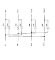
- FIG. 7 is a circuit diagram of the polyphase filter.
- the polyphase filter is provided with four sets of RC filters composed of resistors R10 to R40 and capacitors C10 to C40 in parallel, and four-phase input signals Iin, Qin are applied to the input side terminals (left side terminals) of the resistors R10 to R40.
- Iin_b, Qin_b are input, and the four-phase output signal Iout, Qout, Iout_b and Qout_b are output.
- Iin_b is a negative phase signal of Iin (the phase is different by ⁇ )
- Qin_b is a negative phase signal of Qin.
- Iin and Qin have a phase difference of ⁇ / 2. The same applies to the output signal.
- capacitors C10 to C40 are connected to the input sides of the resistors R40, R10, R20, and R30, respectively, and four sets of filters are connected clockwise (or counterclockwise).
- the resistors R10 to R40 have the same resistance value, and the capacitors C10 to C40 have the same capacitance value.
- the phase relationship of the four-phase input signal is low in accuracy, and when passing through the polyphase filter, the phase relationship of the four-phase output signal becomes high accuracy.
- the principle is described in Non-Patent Document 1 described above, but the RC filter can be regarded as a low-pass filter or a high-pass filter. Since such a filter has a phase shift of 90 ° ( ⁇ / 2) in the cutoff frequency band, by connecting four sets of RC filters clockwise, the right terminal of the resistor R, which is the output of the RC filter, A four-phase output signal with a phase shifted by 90 ° ( ⁇ / 2) with high accuracy is generated.
- the polyphase filter PPF can generate the four-phase first local frequency signal LO (DMIX) only in the vicinity of the cutoff frequency Fc of the four sets of filters constituting the polyphase filter.
- the input signal is not necessarily a four-phase input signal
- the two-phase input signals Iin and Iin_b may be input to the resistors R10 and R20 and the resistors R30 and R40, respectively.
- a single-phase input signal may be input to all the resistors R10 to R40.
- the phase relationship of the four output signals is formed with high accuracy in a relationship that gradually shifts by 90 °.
- the signal is attenuated by passing through the number of stages, a large number of stages is not preferable.
- FIG. 8 is a block diagram of a two-stage (secondary) polyphase filter.
- This example includes a first-stage polyphase filter PPF1 and a second-stage polyphase filter PPF2.
- the first-stage polyphase filter PPF1 receives the two-phase input signals LOin and LOin_b, and the four outputs of the first stage are connected to the four inputs of the second stage, and 4 from the four output terminals of the second stage.
- Phase output signals LOout (0) to LOout (3 ⁇ / 2) are output.
- a filter is composed of a resistor R1 and a capacitor C1
- a filter is composed of a resistor R2 and a capacitor C2.
- the cutoff frequency Fc1 due to the first-stage resistor R1 and the capacitance C1 is set to 2.5 GHz
- the cutoff frequency Fc2 due to the second-stage resistor R2 and the capacitance C2 is set to 3.5 GHz.
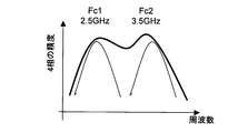
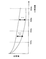
- FIG. 9 is a diagram showing the frequency characteristics of FIG.
- the horizontal axis corresponds to the frequency
- the vertical axis corresponds to the accuracy of the four-phase output.
- the polyphase filter having a two-stage configuration generates a high-precision four-phase signal with the cut-off frequencies Fc1 and Fc2 of each stage, so that the frequency band can be widened to Fc1 to Fc2. it can.
- the amount of signal attenuation increases as the number of stages increases in the polyphase filter, it is not practical to increase the number of stages, so there is a limit to widening the frequency band simply by increasing the number of stages.
- the receiving circuit using the single sideband mixer shown in FIG. 3 processes the received signal RF in a wide frequency band.
- the polyphase filter generates a highly accurate four-phase first local frequency signal LO (DMIX) only in the cut-off frequency band. Therefore, if the frequency band of the polyphase filter can be widened, the frequency band of the single band mixer using the polyphase filter can be widened.
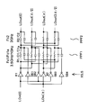
- FIG. 10 is a circuit diagram of the polyphase filter in the present embodiment.
- This example is a single-stage filter that receives two-phase input signals LOi and LOi_b and outputs four-phase output signals LOout (0) to LOout (3 ⁇ / 2).
- the four sets of filters have resistors R10 to R40 having the same resistance value and main capacitors C10 to C40 having the same capacitance value. The configuration so far is the same as FIG.
- the four sets of filters further have sub-capacitances C10a to C40a in parallel with the main capacities C10 to C40.
- the two-phase input signals LOin (0) and LOin ( ⁇ ) are supplied to the input terminals (left terminals) of the resistors R10 and R20 via the buffers B1 and B2.
- one terminal of the sub capacitor C10a is connected to the output terminal (right terminal) of the resistor R10, and the other terminal is supplied with the input signal LOi_b via the switch buffer SB1.
- one terminal of the sub capacitor C20a is connected to the output terminal (right terminal) of the resistor R20, and the other terminal is supplied with the input signal LOi via the switch buffer SB2.
- One terminal of the sub capacitor C30a is connected to the output terminal (right terminal) of the resistor R30, and the other terminal is supplied with the input signal LOi via the switch buffer SB3.
- the sub-capacitor C40a has one terminal connected to the output terminal (right terminal) of the resistor R40 and the other terminal supplied with the input signal LOi_b via the switch buffer SB4.
- FIG. 11 is a circuit diagram of the input buffer and the switch buffer of the polyphase filter in the present embodiment.
- the switch buffer SB includes an inverter circuit including a P-channel transistor P1 and an N-channel transistor N1, and a P-channel transistor P3 and an N-channel transistor N4 that are controlled by opposite-phase switch signals XS and S, respectively. Therefore, when the switch signals XS and S become H level and L level, respectively, the switch buffer SB turns off the transistors P3 and N4 and enters an output high impedance state (off state). Further, when the switch signals XS and S become L level and H level, respectively, the transistors P3 and N4 are turned on, and a normal inverter circuit is formed (ON state).
- the input buffer B is an inverter circuit composed of transistors P1 and N2.
- the input buffer B may have the same circuit configuration as the switch buffer SB, and the switch signals XS and S may be constantly maintained at the L level and the H level to be used as an inverter circuit. In that case, the operations of the buffer B and the switch buffer SB are equivalent, and a balance is rather preferable.
- the input signal LOi_b is input to the main capacitor C10 and the sub capacitor C10a through the input buffer B3 and the switch buffer SB1. Therefore, when the switch buffer SB1 is in the on state (non-high impedance state), the left terminal of the sub capacitor C10a and the left terminal of the main capacitor C10 are in the same signal state and are substantially short-circuited. As a result, the main capacity C10 and the sub capacity C10a are substantially the same as the configuration connected in parallel. On the other hand, when the switch buffer SB1 is in the off state (high impedance state), it is substantially the same as when the sub capacitor C10a does not exist.
- the cutoff frequency of the polyphase filter of FIG. 10 can be set to two desired frequencies. As a result, it is possible to substantially widen the operating frequency band by controlling the operating frequency band of the single-phase polyphase filter of FIG. 10 to the high band and the low band by switching the switch signals XS and S. it can.
- FIG. 12 is another circuit diagram of the polyphase filter of the present embodiment.
- four-phase input signals LOin (0), LOin ( ⁇ / 2), LOin ( ⁇ ), and LOin (3 ⁇ / 2) are input, and each input signal is input to input buffers B1 to B4.
- input signals LOin (3 ⁇ / 2), LOin (0), LOin ( ⁇ / 2), and LOin ( ⁇ ) are supplied to the sub capacitors C10a to C40a via the switch buffers SB1 to SB4, respectively.
- the operating principle is the same as in FIG.
- the polyphase filter can also be applied to a case where a single input signal is supplied to the input terminals of the resistors R10 to R40 via one input buffer B, respectively.
- a single input signal may be supplied to the four sub capacitors C10a to C40a via the four switch buffers SB1 to SB4.
- the switch buffers SB1 to SB4 and the second switch buffers SB1b to SB4b may be controlled by different switch signals.
- the filter is composed of the third cutoff frequency when the filter is composed of only the main capacitor and the second sub capacitors C10b to C40b, and the main capacitor and the first and second sub capacitors C10a to C40a and C10b to C40b. It is possible to switch to the fourth cut-off frequency. As a result, a wider frequency band can be realized.
- FIG. 13 is a circuit diagram of the polyphase filter in the present embodiment.
- a main capacitor C1 and a sub-capacitor C1a are provided in parallel in the first stage of a two-stage filter. That is, the configuration of the first-stage polyphase filter PPF1 is the same as that in FIG. 10, and the configuration of the second-stage polyphase filter PPF2 is the same as that in FIG.
- the first set of four RC filters to which the two-phase input signals LOin (0) and LOin ( ⁇ ) are input are provided with a resistor R1, a main capacitor C1, and a sub capacitor C1a.
- the filter is provided with a resistor R2 and a capacitor C2.
- Switch signals XS and S are supplied to the switch buffers SB1 to SB4.
- the cut-off frequency of the first-stage polyphase filter PPF1 is high because the switch buffers SB1 to SB4 are in a high impedance state when the switch signals XS and S are at the H and L levels.
- the switch buffers SB1 to SB4 are in a non-high impedance state (conducting state) when the switch signals XS and S are at the L and H levels.
- the cutoff frequency Fc2 of the second-stage polyphase filter PPF2 is a frequency due to the resistor R2 and the capacitor C2.
- Fc2 1 / 2 ⁇ R2C2 become.
- Fc2 2GHz is shown as an example.
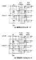
- FIG. 14 is a diagram when the polyphase filter of FIG. 13 is used in a high frequency mode and a low frequency mode.
- the switch signals XS and S are at the H and L levels, and the switch buffers SB1 to SB4 are in a high impedance state.
- the input signal LOin (0), LOin ( ⁇ ) is not supplied to the sub capacitor C1a. Therefore, the first stage has a high cutoff frequency Fc1.
- the switch signals XS and S are at the L and H levels, and the switch buffers SB1 to SB4 are in the non-high impedance state (conducting state).
- the input signal LOin (0), LOin ( ⁇ ) is supplied to the sub capacitor C1a. Therefore, the first stage has a low cutoff frequency Fc1a.
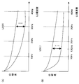
- FIG. 15 is a diagram showing the frequency characteristics of the polyphase filter of FIG.
- the frequency band of the polyphase filter can be switched between the high frequency band LO (H) and the low frequency band LO (L). Therefore, if the switch signal is controlled according to the frequency band of the input signal RF processed by the single sideband mixer, the input signal RF in a substantially wide frequency band can be processed.
- FIG. 16 is a diagram showing a simulation result of the present embodiment by the present inventors.
- the present inventors performed a simulation on the polyphase filter of FIG. 13 and investigated the phase relationship between output signals in the case of the high frequency band LO (H) and the case of the low frequency band LO (L).
- the horizontal axis corresponds to the output frequency
- the vertical axis corresponds to the phase
- the relationship between the two frequencies versus phase is shown.
- the switch signals XS and S are set to the H and L levels and the switch buffers SB1 to SB4 are set in the high impedance state
- the phase difference between the two output signals is 90 ° with high accuracy in a band centering on the frequency of 3 GHz.
- FIG. 17 is a diagram showing a simulation result of the polyphase filter of FIG. 8 by the present inventors.
- the phase difference between the two output signals is 90 ° with high accuracy in the band centered at the frequency of 3 GHz, but the phase difference is smaller than 90 ° in the vicinity of 1.5 GHz. Therefore, it is not preferable to use this polyphase filter in the 1.5 GHz band, and the frequency band is narrow.
- FIG. 18 is a circuit diagram of another polyphase filter in the present embodiment.
- This polyphase filter has a second-stage filter PPF2 to an N-th stage filter PPFn in addition to the first-stage filter PPF1, and has an N-stage (N-order) configuration as a whole.
- the first stage filter PPF1 has the same configuration as the first stage filter PPF1 in FIG. 13, and the second to Nth stage filters PPF2 to PPFn have the same configuration as the second stage filter PPF2 in FIG. Value and capacity value are different.
- Only the first-stage polyphase filter PPF1 has a main capacitor C1 and a subcapacitor C1a together with a resistor R1, and can be switched between a high cutoff frequency Fc1 and a low cutoff frequency Fc1a by switch signals XS, S. .
- the second to Nth stage filters PPF2 to PPFn have different resistance values or capacitance values, and have cutoff frequencies Fc2 to Fcn that are slightly shifted from each other. Then, as in FIG. 13, a two-phase input signal is input, and a four-phase output signal is generated.
- FIG. 19 is a diagram showing frequency characteristics of the polyphase filter of FIG.
- the two cutoff frequencies Fc1 and Fc1a of the first-stage filter PPF1 become the maximum frequency and the minimum frequency, respectively, and the cutoff frequencies Fc2 to Fcn of the second-stage to N-th stage filters PPF2 to PPFn are distributed in the frequency domain between them.
- the resistance value and the capacitance value of each filter are set.
- the operating frequency band of the polyphase filter can be switched between a high frequency band indicated by a solid line and a low frequency band indicated by a broken line in FIG.
- Fc1-Fo2 Fo2-Fc1a
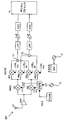
- FIG. 20 is a diagram of a receiving circuit of the single sideband mixer in the present embodiment.
- This receiving circuit amplifies the received signal RF received by the antenna AT by the low noise amplifier LNA, and the amplified signal is multiplied by the first local frequency signals LOI and LOQ by the two mixers M1 and M2 of the down-conversion mixer DMIX. Is done.
- the first local frequency signals LOI and LOQ are a cosine wave and a sine wave whose phases are shifted by 90 °.
- the down-converting mixer DMIX has two mixers M1 and M2 on the positive phase side and two mixers M1 and M2 on the negative phase side (negative phase side). Then, the first local frequency signals LOI, LOQ on the positive phase side and the first local frequency signals -LOI, -LOQ on the negative phase side are respectively supplied to the corresponding two mixers M1, M2.
- the polyphase filter PPF has the same configuration as that of the above-described embodiment, receives a signal (for example, a single-phase, two-phase, or four-phase signal) generated by the oscillator 10 and inputs the first local signal of the four phases. Frequency signals LOI, LOQ, -LOI, -LOQ are generated. Then, the frequency control circuit FCON supplies the switch signals XS, S to the polyphase filter PPF and switches the switch signals XS, S to switch the frequency band between the high frequency side and the low frequency side.
- a signal for example, a single-phase, two-phase, or four-phase signal
- Frequency signals LOI, LOQ, -LOI, -LOQ are generated. Then, the frequency control circuit FCON supplies the switch signals XS, S to the polyphase filter PPF and switches the switch signals XS, S to switch the frequency band between the high frequency side and the low frequency side.
- the quadrature demodulation circuit QDEM subsequent to the down-conversion mixer DMIX has four mixers M3, M4, M5, M6, an adder 12 and a subtractor 13.
- the mixers M3 and M6 are supplied with the second local frequency signal LOBI, and the mixers M4 and M5 are supplied with the second local frequency signal LOBQ.
- These signals LOBI and LOBQ are a cosine wave and a sine wave whose phases are different from each other by 90 °.
- the quadrature demodulation circuit QDEM has a differential configuration, four mixers M3 to M6 are provided on the positive phase side and the negative phase side, respectively, and the second local frequency signals LOBI and LOBQ are supplied to the positive phase side mixer.
- the second local frequency signals -LOBI and -LOBQ having opposite phases are supplied to the mixer on the opposite phase side.
- These four-phase second local frequency signals are generated by the divider DIV. Further, the signal generated by the oscillator 11 is supplied to the frequency divider DIV, and the frequency divider generates a four-phase signal.
- the frequency control circuit FCON switches the switch signals XS and S corresponding to the frequency band of the reception signal RF, and switches the frequency band between the high frequency side and the low frequency side.
- the output of the adder 12 and the output of the subtractor 13 are supplied to the digital processor 14 via a low-pass filter LPF, a variable amplifier, and an AD converter ADC.
- the digital processor 14 performs a decoding process necessary for the receiving circuit.
- the above adder 12 may be a subtracter.
- the subtracter 13 is an adder.
- FIG. 21 is a diagram of a transmission circuit of a single sideband mixer in the present embodiment.
- the I signal component and the Q signal component are supplied to the quadrature modulation circuit QMOD via the variable amplifier VGA and the low pass filter LPF.
- the quadrature modulation circuit QMOD has four mixers M13 to M16, and two local frequency signals LO (QMOD) (cosine wave and sine wave) generated by the frequency divider DIV are shifted by 90 ° as shown in the figure. Supplied.
- An adder 22 that adds the outputs of the mixers M13 and M15 and a subtractor 23 that subtracts the outputs of the mixers M14 and M16 are provided.
- the quadrature modulation circuit QMOD When the quadrature modulation circuit QMOD has a differential configuration, four mixers M13 to M16 are provided on the positive phase side and the negative phase side, respectively, and two local frequency signals LO (QMOD) for the positive phase and the negative phase are supplied.
- the adder 22 may be a subtracter, in which case the subtracter 23 is an adder.
- the up-conversion mixer MIX has two mixers M11 and M12, and is supplied with two local frequency signals whose phases generated by the polyphase filter PPF are shifted by 90 °.
- two mixers M11 and M12 are provided on the positive phase side and the negative phase side, respectively, and a four-phase local frequency signal is supplied from the polyphase filter PPF to the corresponding mixer.
- the adder 24 may be a subtracter.
- the frequency control circuit FCON switches the switch signals XS and S corresponding to the frequency band of the transmission signal RF, and switches the frequency band between the high frequency side and the low frequency side.
- the polyphase filter PPF according to the present embodiment can generate a four-phase signal having a phase difference of 90 ° with high accuracy in a wide frequency band.
- a single sideband mixer using the polyphase filter PPF as a means for generating a local frequency signal can receive a reception signal in a wide frequency band or transmit a transmission signal.
- the single sideband mixer having the polyphase filter PPF can be used for a communication device, for example.
- LOin (0), LOin ( ⁇ ) Input signal LOout (0), LOout ( ⁇ / 2), LOout ( ⁇ ) LOout (3 ⁇ / 2): 4 phase output signal
- R10 to R40 Resistance C10 to C40: Main capacity C10a to C40a: Sub capacity B1, B3: Input buffer SB1 to SB4: First to fourth switch buffers (tri-state buffers) XS, S: Switch signal
Landscapes
- Chemical & Material Sciences (AREA)
- Organic Chemistry (AREA)
- Superheterodyne Receivers (AREA)
- Filters And Equalizers (AREA)
- Transmitters (AREA)
- Networks Using Active Elements (AREA)
Abstract
Description
入力端と出力端とをそれぞれ有する第1~第4の抵抗と,
前記第1の抵抗の出力端と前記第4の抵抗の入力端との間に設けられた第1の主容量と,
前記第2の抵抗の出力端と前記第1の抵抗の入力端との間に設けられた第2の主容量と,
前記第3の抵抗の出力端と前記第2の抵抗の入力端との間に設けられた第3の主容量と,
前記第4の抵抗の出力端と前記第3の抵抗の入力端との間に設けられた第4の主容量と,
前記入力信号を入力し前記第1~第4の抵抗の入力端にそれぞれ出力する入力バッファと,
前記第1の抵抗の出力端に前記第1の主容量と並列に接続された第1の副容量と,前記第4の抵抗の入力端に入力される前記入力信号を入力し前記第1の副容量に出力する第1のスイッチバッファと,
前記第2の抵抗の出力端に前記第2の主容量と並列に接続された第2の副容量と,前記第1の抵抗の入力端に入力される前記入力信号を入力し前記第2の副容量に出力する第2のスイッチバッファと,
前記第3の抵抗の出力端に前記第3の主容量と並列に接続された第3の副容量と,前記第2の抵抗の入力端に入力される前記入力信号を入力し前記第3の副容量に出力する第3のスイッチバッファと,
前記第4の抵抗の出力端に前記第4の主容量と並列に接続された第4の副容量と,前記第3の抵抗の入力端に入力される前記入力信号を入力し前記第4の副容量に出力する第4のスイッチバッファと,
を有し,
前記第1~第4の抵抗の出力端からそれぞれ前記第1~第4の出力信号が出力され,
前記第1~第4のスイッチバッファはスイッチ信号に応答して出力ハイインピーダンス状態か否かに制御される。
I=RF・cos(wlo1t+wlo2t)
になる。
Q=RF・sin(wlo1t+wlo2t)
になる。よって,Q信号側も入力高周波信号RFのみがベースバンドBBにダウンコンバートされ,不要波信号UDはベースバンドBBにダウンコンバートされず,不要波信号UDは除去される。
Qout, Iout_b, Qout_bを出力する。Iin_bはIinの逆相信号(位相がπ異なる)であり,Qin_bはQinの逆相信号である。また,IinとQinとは位相がπ/2異なる。出力信号も同様である。さらに,各容量C10~C40がそれぞれ抵抗R40,R10,R20,R30の入力側に接続され,4組のフィルタが時計回り(または反時計回り)に接続される。抵抗R10~R40は等しい抵抗値を有し,容量C10~C40も等しい容量値を有する。
Fc=1/(2πRC)
である。
Fc=1/(2πR10・(C10+C10a))
になるのに対して,スイッチバッファSB1がオフ状態(ハイインピーダンス状態)の場合は,カットオフ周波数Fcは,
Fc=1/(2πR10・C10)
になる。
Fc1=1/2πR1C1
Fc1a=1/2πR1(C1+C1a)
となる。図中のFc1=3.5GHz,Fc1a=1GHzは,一例である。
Fc2=1/2πR2C2
になる。図中では,Fc2=2GHzが一例として示されている。
LOin(π)は,副容量C1aには供給されない。よって,初段は高いカットオフ周波数Fc1になっている。
LOin(π)は,副容量C1aに供給される。よって,初段は低いカットオフ周波数Fc1aになっている。
Fc1=1/2πR1C1
Fc1a=1/2πR1(C1+C1a)
Fc2=1/2πR2C2
を,次の関係,
Fc2-Fc1a
= Fc1-Fc2
になるように抵抗R1,R2や容量C1,C1a,C2を設定することが好ましい。このよう設定することで,図15の周波数特性は,高い周波数帯域LO(H)の場合の特性と,低い周波数帯域LO(L)の場合の特性とを,周波数Fc2を中心として左右対称にすることができる。それにより,ポリフェーズフィルタが,高い周波数帯域モードと低い周波数帯域モードとで,同等の特性を持つことができる。
Fc1=1/2πR1C1
Fc1a=1/2πR1(C1+C1a)
となる。さらに,2段目~N段目のフィルタPPF2~PPFnのカットオフ周波数Fc2~Fcn の平均周波数は,
Fo2=(1/(2πR2C2)+・・・+1/(2πRnCn))/(n-1)
となる。
Fc1-Fo2 = Fo2-Fc1a
の関係が満たされるように,各フィルタ段での抵抗値,容量値が設定されることが望ましい。そのように設定することで,ポリフェーズフィルタが,高い周波数帯域モードと低い周波数帯域モードとで,同等の特性を持つことができる。
LOout(0),
LOout(π/2), LOout(π) LOout(3π/2):4相の出力信号
R10~R40:抵抗
C10~C40:主容量
C10a~C40a:副容量
B1,B3:入力バッファ
SB1~SB4:第1~第4のスイッチバッファ(トライステートバッファ)
XS,S:スイッチ信号
Claims (13)
- 入力信号を入力し,4相の第1~第4の出力信号を出力するポリフェーズフィルタであって,
入力端と出力端とをそれぞれ有する第1~第4の抵抗と,
前記第1の抵抗の出力端と前記第4の抵抗の入力端との間に設けられた第1の主容量と,
前記第2の抵抗の出力端と前記第1の抵抗の入力端との間に設けられた第2の主容量と,
前記第3の抵抗の出力端と前記第2の抵抗の入力端との間に設けられた第3の主容量と,
前記第4の抵抗の出力端と前記第3の抵抗の入力端との間に設けられた第4の主容量と,
前記入力信号を入力し前記第1~第4の抵抗の入力端にそれぞれ出力する入力バッファと,
前記第1の抵抗の出力端に前記第1の主容量と並列に接続された第1の副容量と,前記第4の抵抗の入力端に入力される前記入力信号を入力し前記第1の副容量に出力する第1のスイッチバッファと,
前記第2の抵抗の出力端に前記第2の主容量と並列に接続された第2の副容量と,前記第1の抵抗の入力端に入力される前記入力信号を入力し前記第2の副容量に出力する第2のスイッチバッファと,
前記第3の抵抗の出力端に前記第3の主容量と並列に接続された第3の副容量と,前記第2の抵抗の入力端に入力される前記入力信号を入力し前記第3の副容量に出力する第3のスイッチバッファと,
前記第4の抵抗の出力端に前記第4の主容量と並列に接続された第4の副容量と,前記第3の抵抗の入力端に入力される前記入力信号を入力し前記第4の副容量に出力する第4のスイッチバッファと,
を有し,
前記第1~第4の抵抗の出力端からそれぞれ前記第1~第4の出力信号が出力され,
前記第1~第4のスイッチバッファはスイッチ信号に応答して出力ハイインピーダンス状態か否かに制御されるポリフェーズフィルタ。 - 入力信号を入力し,4相の第1~第4の出力信号を出力するポリフェーズフィルタであって,
前記入力信号を入力し4相の信号を出力する第1段のフィルタ単位回路と,
前記第1段のフィルタ単位回路が出力する4相の信号を入力する第2段のフィルタ単位回路とを有し,
前記第1段,第2段のフィルタ単位回路は,それぞれ,
入力端と出力端とをそれぞれ有する第1~第4の抵抗と,
前記第1の抵抗の出力端と前記第4の抵抗の入力端との間に設けられた第1の主容量と,
前記第2の抵抗の出力端と前記第1の抵抗の入力端との間に設けられた第2の主容量と,
前記第3の抵抗の出力端と前記第2の抵抗の入力端との間に設けられた第3の主容量と,
前記第4の抵抗の出力端と前記第3の抵抗の入力端との間に設けられた第4の主容量とを有し,
前記第1段のフィルタ単位回路において,
前記入力信号を入力し前記第1~第4の抵抗の入力端にそれぞれ出力する入力バッファと,
前記第1の抵抗の出力端に前記第1の主容量と並列に接続された第1の副容量と,前記第4の抵抗の入力端に入力される前記入力信号を入力し前記第1の副容量に出力する第1のスイッチバッファと,
前記第2の抵抗の出力端に前記第2の主容量と並列に接続された第2の副容量と,前記第1の抵抗の入力端に入力される前記入力信号を入力し前記第2の副容量に出力する第2のスイッチバッファと,
前記第3の抵抗の出力端に前記第3の主容量と並列に接続された第3の副容量と,前記第2の抵抗の入力端に入力される前記入力信号を入力し前記第3の副容量に出力する第3のスイッチバッファと,
前記第4の抵抗の出力端に前記第4の主容量と並列に接続された第4の副容量と,前記第3の抵抗の入力端に入力される前記入力信号を入力し前記第4の副容量に出力する第4のスイッチバッファと,
を有し,
前記第2段の単位フィルタ回路の前記第1~第4の抵抗の出力端からそれぞれ前記第1~第4の出力信号が出力され,
前記第1~第4のスイッチバッファはスイッチ信号に応答して出力ハイインピーダンス状態か否かに制御されるポリフェーズフィルタ。 - 請求項1または2において,
前記入力信号は,互いに位相が異なる第1,第2の入力信号を有し,
前記入力バッファは,前記第1の入力信号を入力し前記第1及び第2の抵抗の入力端子に出力する第1の入力バッファと,前記第2の入力信号を入力し前記第3及び第4の抵抗の入力端子に出力する第2の入力バッファとを有するポリフェーズフィルタ。 - 請求項1または2において,
前記入力信号は,互いに位相が異なる第1~第4の入力信号を有し,
前記入力バッファは,
前記第1~第4の入力信号をそれぞれ入力し,前記第1~第4の抵抗の入力端子にそれぞれ出力する第1~第4の入力バッファを有するポリフェーズフィルタ。 - 請求項2において,
前記第1段の単位フィルタ回路の前記抵抗と主容量とに対応する第1の周波数と,前記第2段の単位フィルタ回路の前記抵抗と主容量とに対応する第2の周波数との差が,前記第1段の単位フィルタ回路の前記抵抗と主容量及び副容量とに対応する第3の周波数と,前記第2の周波数との差と等しくなるように,前記第1段の単位フィルタ回路の前記主容量と副容量の容量が設定されているポリフェーズフィルタ。 - 請求項2において,
さらに,前記第2段の単位フィルタ回路の出力に接続された第3段~第N段の単位フィルタ回路を有し,
前記第1~第4の出力信号が,前記第N段の単位フィルタ回路の前記第1~第4の抵抗の出力端からそれぞれ出力され,
前記第1段の単位フィルタ回路の前記抵抗と主容量とに対応する第1の周波数と,前記第2段~第N段の単位フィルタ回路の前記抵抗と主容量とに対応する第2~第Nの周波数の平均周波数との差が,前記第1段の単位フィルタ回路の前記抵抗と主容量及び副容量とに対応する第3の周波数と,前記平均周波数との差と等しくなるように,前記第1段の単位フィルタ回路の前記主容量と副容量の容量が設定されているポリフェーズフィルタ。 - 請求項1または2において,
前記入力バッファの駆動能力と前記第1~第4のスイッチバッファの駆動能力との比が,前記主容量と前記副容量との容量比に等しいポリフェーズフィルタ。 - 互いに位相が異なる第1,第2の入力信号を入力し,4相の第1~第4の出力信号を出力するポリフェーズフィルタにおいて,
入力端と出力端とをそれぞれ有する第1~第4の抵抗と,
前記第1の抵抗の出力端と前記第4の抵抗の入力端との間に設けられた第1の主容量と,
前記第2の抵抗の出力端と前記第1の抵抗の入力端との間に設けられた第2の主容量と,
前記第3の抵抗の出力端と前記第2の抵抗の入力端との間に設けられた第3の主容量と,
前記第4の抵抗の出力端と前記第3の抵抗の入力端との間に設けられた第4の主容量と,
前記第1の入力信号を入力し前記第1及び第2の抵抗の入力端に出力する第1のバッファと,
前記第2の入力信号を入力し前記第3及び第4の抵抗の入力端に出力する第2のバッファと,
前記第1の抵抗の出力端に前記第1の主容量と並列に接続された第1の副容量と,前記第2の入力信号を入力し前記第1の副容量に出力する第1のスイッチバッファと,
前記第2の抵抗の出力端に前記第2の主容量と並列に接続された第2の副容量と,前記第1の入力信号を入力し前記第2の副容量に出力する第2のスイッチバッファと,
前記第3の抵抗の出力端に前記第3の主容量と並列に接続された第3の副容量と,前記第1の入力信号を入力し前記第3の副容量に出力する第3のスイッチバッファと,
前記第4の抵抗の出力端に前記第4の主容量と並列に接続された第4の副容量と,前記第2の入力信号を入力し前記第4の副容量に出力する第4のスイッチバッファと,
を有し,
前記第1~第4の抵抗の出力端からそれぞれ前記第1~第4の出力信号が出力され,
前記第1~第4のスイッチバッファはスイッチ信号に応答して出力ハイインピーダンス状態か否かに制御されるポリフェーズフィルタ。 - 互いに位相が異なる第1~第4の入力信号を入力し,4相の第1~第4の出力信号を出力するポリフェーズフィルタにおいて,
入力端と出力端とをそれぞれ有する第1~第4の抵抗と,
前記第1の抵抗の出力端と前記第4の抵抗の入力端との間に設けられた第1の主容量と,
前記第2の抵抗の出力端と前記第1の抵抗の入力端との間に設けられた第2の主容量と,
前記第3の抵抗の出力端と前記第2の抵抗の入力端との間に設けられた第3の主容量と,
前記第4の抵抗の出力端と前記第3の抵抗の入力端との間に設けられた第4の主容量と,
前記第1~第4の入力信号をそれぞれ入力し前記第1~第4の抵抗の入力端にそれぞれ出力する第1~第4のバッファと,
前記第1の抵抗の出力端に前記第1の主容量と並列に接続された第1の副容量と,前記第4の入力信号を入力し前記第1の副容量に出力する第1のスイッチバッファと,
前記第2の抵抗の出力端に前記第2の主容量と並列に接続された第2の副容量と,前記第1の入力信号を入力し前記第2の副容量に出力する第2のスイッチバッファと,
前記第3の抵抗の出力端に前記第3の主容量と並列に接続された第3の副容量と,前記第2の入力信号を入力し前記第3の副容量に出力する第3のスイッチバッファと,
前記第4の抵抗の出力端に前記第4の主容量と並列に接続された第4の副容量と,前記第3の入力信号を入力し前記第4の副容量に出力する第4のスイッチバッファと,
を有し,
前記第1~第4の抵抗の出力端からそれぞれ前記第1~第4の出力信号が出力され,
前記第1~第4のスイッチバッファはスイッチ信号に応答して出力ハイインピーダンス状態か否かに制御されるポリフェーズフィルタ。 - 請求項1,2,5,6,8,9のいずれかに記載のポリフェーズフィルタであって,前記入力信号として第1のローカル周波数信号が入力されるポリフェーズフィルタと,
高周波入力信号と前記ポリフェーズフィルタの第1または第3,または第1及び第3の出力信号とを乗算する第1のミキサと,前記高周波入力信号と前記ポリフェーズフィルタの第2または第4,または第2及び第4の出力信号とを乗算する第2のミキサとを有するダウンコンバートミキサと,
前記第1,第2のミキサの出力と第2のローカル周波数信号とをそれぞれ乗算する第3,第4のミキサと,当該第3,第4のミキサの出力を加算または減算してI信号を出力する第1の加減算器と,前記第1,第2のミキサの出力と前記第2のローカル周波数信号とをそれぞれ乗算する第5,第6のミキサと,当該第5,第6のミキサの出力を減算または加算してQ信号を出力する第2の加算減器とを有する直交復調回路とを有する受信側シングルバンドミキサ。 - 請求項10において,さらに,
受信周波数帯域に応じて,前記スイッチ信号を前記第1~第4のスイッチバッファに供給し,前記ハイインピーダンス状態か否かに制御する周波数帯域制御ユニットを有する受信側シングルバンドミキサ。 - I信号と第2のローカル周波数信号とをそれぞれ乗算する第3,第4のミキサと,Q信号と前記第2のローカル周波数信号とをそれぞれ乗算する第5,第6のミキサと,前記第3と第5のミキサの出力を加算または減算する第1の加減算器と,前記第4と第6のミキサの出力を減算または加算する第2の加減算器とを有する直交変調回路と,
請求項1,2,5,6,8,9のいずれかに記載のポリフェーズフィルタであって,前記入力信号として第1のローカル周波数信号が入力されるポリフェーズフィルタと,
前記第1の加減算器の出力信号と前記ポリフェーズフィルタの第1または第3,または第1及び第3の出力信号とを乗算する第1のミキサと,前記第2の加減算器の出力信号と前記ポリフェーズフィルタの第2または第4,または第2及び第4の出力信号とを乗算する第2のミキサとを有するアップコンバートミキサとを有する送信側シングルバンドミキサ。 - 請求項12において,さらに,
送信周波数帯域に応じて,前記スイッチ信号を前記第1~第4のスイッチバッファに供給し,前記ハイインピーダンス状態か否かに制御する周波数帯域制御ユニットを有する送信側シングルバンドミキサ。
Priority Applications (4)
| Application Number | Priority Date | Filing Date | Title |
|---|---|---|---|
| CN2009801603323A CN102474236A (zh) | 2009-07-06 | 2009-07-06 | 多相滤波器以及具有该多相滤波器的单边带混频器 |
| PCT/JP2009/003131 WO2011004423A1 (ja) | 2009-07-06 | 2009-07-06 | ポリフェーズフィルタ及びそれを有するシングルサイドバンドミキサ |
| JP2011521699A JP5360210B2 (ja) | 2009-07-06 | 2009-07-06 | ポリフェーズフィルタ及びそれを有するシングルサイドバンドミキサ |
| US13/333,471 US8797111B2 (en) | 2009-06-26 | 2011-12-21 | Poly-phase filter, and a single-side band mixer including the same |
Applications Claiming Priority (1)
| Application Number | Priority Date | Filing Date | Title |
|---|---|---|---|
| PCT/JP2009/003131 WO2011004423A1 (ja) | 2009-07-06 | 2009-07-06 | ポリフェーズフィルタ及びそれを有するシングルサイドバンドミキサ |
Related Child Applications (1)
| Application Number | Title | Priority Date | Filing Date |
|---|---|---|---|
| US13/333,471 Continuation US8797111B2 (en) | 2009-06-26 | 2011-12-21 | Poly-phase filter, and a single-side band mixer including the same |
Publications (1)
| Publication Number | Publication Date |
|---|---|
| WO2011004423A1 true WO2011004423A1 (ja) | 2011-01-13 |
Family
ID=43428865
Family Applications (1)
| Application Number | Title | Priority Date | Filing Date |
|---|---|---|---|
| PCT/JP2009/003131 Ceased WO2011004423A1 (ja) | 2009-06-26 | 2009-07-06 | ポリフェーズフィルタ及びそれを有するシングルサイドバンドミキサ |
Country Status (4)
| Country | Link |
|---|---|
| US (1) | US8797111B2 (ja) |
| JP (1) | JP5360210B2 (ja) |
| CN (1) | CN102474236A (ja) |
| WO (1) | WO2011004423A1 (ja) |
Cited By (1)
| Publication number | Priority date | Publication date | Assignee | Title |
|---|---|---|---|---|
| JP2015201679A (ja) * | 2014-04-04 | 2015-11-12 | 三菱電機株式会社 | 複数チャンネル同時受信装置 |
Families Citing this family (9)
| Publication number | Priority date | Publication date | Assignee | Title |
|---|---|---|---|---|
| US9252743B2 (en) * | 2012-09-28 | 2016-02-02 | Intel Corporation | Distributed polyphase filter |
| CN104113299B (zh) * | 2013-04-17 | 2017-04-12 | 凌力尔特公司 | 具有相位调谐的多相位滤波器 |
| US9762284B2 (en) * | 2015-04-06 | 2017-09-12 | Analog Devices, Inc. | Circuits and systems for transmitter calibration |
| WO2017141367A1 (ja) * | 2016-02-17 | 2017-08-24 | 三菱電機株式会社 | ポリフェーズフィルタおよびフィルタ回路 |
| US10044321B2 (en) * | 2016-08-02 | 2018-08-07 | Samsung Electronics Co., Ltd | System and method for linearizing a transmitter by rejecting harmonics at mixer output |
| CN108900202B (zh) * | 2018-06-13 | 2020-10-27 | 华南理工大学 | 一种并行的频点灵活可调的∑-δ调制器及其工作方法 |
| CN111131964A (zh) * | 2019-11-18 | 2020-05-08 | 中山市天键通讯技术有限公司 | 通过开关调整的rc调音分频电路 |
| US11271710B1 (en) * | 2020-11-30 | 2022-03-08 | Renesas Electronics Corporation | Wideband quadrature phase generation using tunable polyphase filter |
| US11811413B2 (en) * | 2021-10-13 | 2023-11-07 | Mediatek Inc. | Poly phase filter with phase error enhance technique |
Citations (4)
| Publication number | Priority date | Publication date | Assignee | Title |
|---|---|---|---|---|
| JP2001045080A (ja) * | 1999-07-26 | 2001-02-16 | Nippon Telegr & Teleph Corp <Ntt> | 振幅整合型ポリフェーズフィルタおよび位相振幅整合型ポリフェーズフィルタならびにイメージ抑圧型受信機 |
| US20040116096A1 (en) * | 2002-12-10 | 2004-06-17 | Irf Semiconductor, Inc. | Radio frequency receiver architecture with tracking image-reject polyphase filtering |
| JP2006121665A (ja) * | 2004-09-24 | 2006-05-11 | Matsushita Electric Ind Co Ltd | イメージリジェクションミキサと能動帯域フィルタを有する受信if回路 |
| WO2008126360A1 (ja) * | 2007-03-29 | 2008-10-23 | Panasonic Corporation | 受信装置とこれを用いた電子機器 |
Family Cites Families (9)
| Publication number | Priority date | Publication date | Assignee | Title |
|---|---|---|---|---|
| JP3125369B2 (ja) | 1991-10-24 | 2001-01-15 | ソニー株式会社 | アクティブハイパスフィルタ及びアクティブローパスフィルタ |
| CA2415917A1 (en) | 2003-01-08 | 2004-07-08 | Sirific Wireless Corporation | Regenerative divider used for up-conversion and down conversion |
| KR101085693B1 (ko) | 2004-03-24 | 2011-11-22 | 조지아 테크 리서치 코오포레이션 | 개선된 광대역 i/q 신호 발생 장치 |
| CN100527598C (zh) * | 2004-03-24 | 2009-08-12 | 三星电子株式会社 | 改进的宽带同相位信号和正交相位信号生成装置 |
| US20060068740A1 (en) * | 2004-09-24 | 2006-03-30 | Matsushita Electric Industrial Co., Ltd. | Receiver if circuit including image rejection mixer and active bandpass filter |
| US20070155350A1 (en) * | 2005-12-29 | 2007-07-05 | Wionics Research | Method of frequency planning in an ultra wide band system |
| US20080132189A1 (en) * | 2006-11-30 | 2008-06-05 | Silicon Laboratories, Inc. | Mixing dac and polyphase filter architectures for a radio frequency receiver |
| CN101197531B (zh) * | 2007-10-30 | 2011-09-14 | 电子科技大学 | 容控数字频率调制电路 |
| JP5360056B2 (ja) * | 2008-05-19 | 2013-12-04 | 日本電気株式会社 | ポリフェーズフィルタの帯域調整装置及びポリフェーズフィルタの帯域調整方法 |
-
2009
- 2009-07-06 WO PCT/JP2009/003131 patent/WO2011004423A1/ja not_active Ceased
- 2009-07-06 JP JP2011521699A patent/JP5360210B2/ja not_active Expired - Fee Related
- 2009-07-06 CN CN2009801603323A patent/CN102474236A/zh active Pending
-
2011
- 2011-12-21 US US13/333,471 patent/US8797111B2/en not_active Expired - Fee Related
Patent Citations (4)
| Publication number | Priority date | Publication date | Assignee | Title |
|---|---|---|---|---|
| JP2001045080A (ja) * | 1999-07-26 | 2001-02-16 | Nippon Telegr & Teleph Corp <Ntt> | 振幅整合型ポリフェーズフィルタおよび位相振幅整合型ポリフェーズフィルタならびにイメージ抑圧型受信機 |
| US20040116096A1 (en) * | 2002-12-10 | 2004-06-17 | Irf Semiconductor, Inc. | Radio frequency receiver architecture with tracking image-reject polyphase filtering |
| JP2006121665A (ja) * | 2004-09-24 | 2006-05-11 | Matsushita Electric Ind Co Ltd | イメージリジェクションミキサと能動帯域フィルタを有する受信if回路 |
| WO2008126360A1 (ja) * | 2007-03-29 | 2008-10-23 | Panasonic Corporation | 受信装置とこれを用いた電子機器 |
Cited By (1)
| Publication number | Priority date | Publication date | Assignee | Title |
|---|---|---|---|---|
| JP2015201679A (ja) * | 2014-04-04 | 2015-11-12 | 三菱電機株式会社 | 複数チャンネル同時受信装置 |
Also Published As
| Publication number | Publication date |
|---|---|
| JPWO2011004423A1 (ja) | 2012-12-13 |
| US8797111B2 (en) | 2014-08-05 |
| JP5360210B2 (ja) | 2013-12-04 |
| US20120092085A1 (en) | 2012-04-19 |
| CN102474236A (zh) | 2012-05-23 |
Similar Documents
| Publication | Publication Date | Title |
|---|---|---|
| JP5360210B2 (ja) | ポリフェーズフィルタ及びそれを有するシングルサイドバンドミキサ | |
| JP4708076B2 (ja) | ダウンコンバータ及びアップコンバータ | |
| KR100444286B1 (ko) | 주파수 변환기 및 이를 이용한 무선통신장치 | |
| WO2009158272A2 (en) | Systems and methods for implementing a harmonic rejection mixer | |
| US8938204B2 (en) | Signal generator circuit and radio transmission and reception device including the same | |
| CN105409118B (zh) | 对在tx驱动放大器中生成的杂散谐波的抑制 | |
| US8521221B2 (en) | Dual mode RF transceiver and receiving method of the same | |
| CN104242823A (zh) | 混频开关电路及混频器 | |
| CN104467686A (zh) | 一种低功耗、低噪声的混频器 | |
| JP2009284059A (ja) | フィルタ回路、無線送信機および無線受信機 | |
| US7085548B1 (en) | Harmonic mixer | |
| US9112482B2 (en) | Receiver | |
| WO2020068340A1 (en) | Capacitor compensated dual of polyphase filter | |
| US7302011B1 (en) | Quadrature frequency doubling system | |
| JP3993573B2 (ja) | 複数の無線システムに対応可能な無線通信装置 | |
| US20050157826A1 (en) | Filtering signals | |
| JP5034126B2 (ja) | 周波数変換装置 | |
| CN115765772A (zh) | 低功耗混频优先型宽带接收机前端模块 | |
| JP5001186B2 (ja) | 乗算回路及び通信装置 | |
| JP4255875B2 (ja) | 広帯域45度移相器 | |
| CN119111039B (zh) | 接收机、射频收发器和终端 | |
| JP6921358B2 (ja) | ミクサ | |
| JP5862658B2 (ja) | 受信回路およびそのフィルタリング方法 | |
| JP2009182928A (ja) | チューナ |
Legal Events
| Date | Code | Title | Description |
|---|---|---|---|
| WWE | Wipo information: entry into national phase |
Ref document number: 200980160332.3 Country of ref document: CN |
|
| 121 | Ep: the epo has been informed by wipo that ep was designated in this application |
Ref document number: 09847028 Country of ref document: EP Kind code of ref document: A1 |
|
| WWE | Wipo information: entry into national phase |
Ref document number: 2011521699 Country of ref document: JP |
|
| NENP | Non-entry into the national phase |
Ref country code: DE |
|
| 122 | Ep: pct application non-entry in european phase |
Ref document number: 09847028 Country of ref document: EP Kind code of ref document: A1 |