WO2011001779A1 - シリコン構造体の製造方法及びその製造装置並びにその製造プログラム - Google Patents
シリコン構造体の製造方法及びその製造装置並びにその製造プログラム Download PDFInfo
- Publication number
- WO2011001779A1 WO2011001779A1 PCT/JP2010/059344 JP2010059344W WO2011001779A1 WO 2011001779 A1 WO2011001779 A1 WO 2011001779A1 JP 2010059344 W JP2010059344 W JP 2010059344W WO 2011001779 A1 WO2011001779 A1 WO 2011001779A1
- Authority
- WO
- WIPO (PCT)
- Prior art keywords
- frequency power
- etching
- manufacturing
- silicon
- plasma
- Prior art date
- Legal status (The legal status is an assumption and is not a legal conclusion. Google has not performed a legal analysis and makes no representation as to the accuracy of the status listed.)
- Ceased
Links
Images



Classifications
-
- H—ELECTRICITY
- H10—SEMICONDUCTOR DEVICES; ELECTRIC SOLID-STATE DEVICES NOT OTHERWISE PROVIDED FOR
- H10P—GENERIC PROCESSES OR APPARATUS FOR THE MANUFACTURE OR TREATMENT OF DEVICES COVERED BY CLASS H10
- H10P50/00—Etching of wafers, substrates or parts of devices
- H10P50/20—Dry etching; Plasma etching; Reactive-ion etching
- H10P50/24—Dry etching; Plasma etching; Reactive-ion etching of semiconductor materials
- H10P50/242—Dry etching; Plasma etching; Reactive-ion etching of semiconductor materials of Group IV materials
- H10P50/244—Dry etching; Plasma etching; Reactive-ion etching of semiconductor materials of Group IV materials comprising alternated and repeated etching and passivation steps
-
- B—PERFORMING OPERATIONS; TRANSPORTING
- B81—MICROSTRUCTURAL TECHNOLOGY
- B81C—PROCESSES OR APPARATUS SPECIALLY ADAPTED FOR THE MANUFACTURE OR TREATMENT OF MICROSTRUCTURAL DEVICES OR SYSTEMS
- B81C1/00—Manufacture or treatment of devices or systems in or on a substrate
- B81C1/00436—Shaping materials, i.e. techniques for structuring the substrate or the layers on the substrate
- B81C1/00523—Etching material
- B81C1/00531—Dry etching
-
- B—PERFORMING OPERATIONS; TRANSPORTING
- B81—MICROSTRUCTURAL TECHNOLOGY
- B81C—PROCESSES OR APPARATUS SPECIALLY ADAPTED FOR THE MANUFACTURE OR TREATMENT OF MICROSTRUCTURAL DEVICES OR SYSTEMS
- B81C2201/00—Manufacture or treatment of microstructural devices or systems
- B81C2201/01—Manufacture or treatment of microstructural devices or systems in or on a substrate
- B81C2201/0101—Shaping material; Structuring the bulk substrate or layers on the substrate; Film patterning
- B81C2201/0111—Bulk micromachining
- B81C2201/0112—Bosch process
Definitions
- the present invention relates to a method of manufacturing a silicon structure, a manufacturing apparatus thereof, and a manufacturing program thereof.
- MEMS Micro Electro Mechanical Systems
- etching process for example, Patent Document 1
- SF 6 sulfur hexafluoride
- protective film forming step of this process carbon fluoride (especially C 4 F 8 ) that forms an organic deposition film has been used as the protective film forming gas.
- the present invention is directed to the development of anisotropic dry etching technology for silicon that achieves high verticality and good sidewall shape by using a gas with a low global warming potential instead of sulfur hexafluoride (SF 6 ) or fluorocarbon. It contributes greatly.
- SF 6 sulfur hexafluoride
- fluorocarbon fluorocarbon
- the object to be processed for example, a silicon substrate
- the object to be processed is set by setting the power applied in the plasma to a specific range. It was confirmed that some deposits were likely to be formed on the surface. Accordingly, the inventors actively utilize the above-described change in the form of the deposit due to the difference in applied power, thereby protecting not only sulfur hexafluoride (SF 6 ) but also a high global warming potential (GWP). It has been found that anisotropic etching of silicon can be performed without using a fluorocarbon gas for film formation. The present invention was created from the above viewpoint.
- One method of manufacturing a silicon structure according to the present invention includes a first step of converting a first iodine fluoride into an etching gas by applying a first high-frequency power, and the above-described first high-frequency power.
- a second step of converting the second iodine fluoride into a plasma using a protective film forming gas by applying a low second high frequency power the silicon region in the object to be processed including the silicon region An etching step.
- the first iodine fluoride is used in place of sulfur hexafluoride (SF 6 ) but also C 4 F 8 that has been used as a protective film forming gas in the past.
- a representative fluorocarbon gas is also not used.
- the etching process in which the first iodine fluoride is turned into plasma and the protective film forming process in which the second iodine fluoride is turned into plasma are alternately repeated, thereby achieving high verticality and good sidewall shape.
- the first high-frequency power is applied to an induction coil (hereinafter also simply referred to as a coil) using a dielectric coupled plasma etching apparatus.
- An etching step is performed by alternately performing the second step of converting to plasma as described above, and applying high frequency power to the stage electrode on which the object to be processed including the silicon region is placed during the first step described above.
- the first iodine fluoride is used in place of sulfur hexafluoride (SF 6 ) but also C 4 F 8 that has been used as a protective film forming gas in the past.
- a representative fluorocarbon gas is also not used.
- the manufacturing program of one silicon structure of the present invention includes a first step of converting the first iodine fluoride into plasma by applying the first high-frequency power, and the first high-frequency power described above.
- a second step of converting the second iodine fluoride into a plasma as a protective film forming gas by applying a lower second high frequency power, the silicon in the workpiece including the silicon region is obtained. Etching the region.
- the first iodine fluoride is used in place of sulfur hexafluoride (SF 6 ) but also C 4 F 8 that has been used as a protective film forming gas.
- a representative fluorocarbon gas is also not used.
- the etching step in which the first iodine fluoride is turned into plasma and the protective film forming step in which the second iodine fluoride is turned into plasma are alternately repeated, thereby achieving high verticality and good sidewall shape.
- another silicon structure manufacturing program of the present invention uses a dielectric coupled plasma etching apparatus to apply a first high-frequency power to an induction coil, thereby converting the first iodine fluoride into an etching gas into a plasma. And a second step of applying a second high-frequency power lower than the first high-frequency power to the induction coil to convert the second iodine fluoride into a plasma as a protective film forming gas.
- the silicon region is etched by applying high-frequency power to the stage electrode on which the workpiece including the silicon region is placed.
- the first iodine fluoride is used in place of sulfur hexafluoride (SF 6 ) but also C 4 F 8 that has been used as a protective film forming gas.
- a representative fluorocarbon gas is also not used.
- an etching step in which the first iodine fluoride is turned into plasma by the dielectric coupling type plasma etching apparatus and a protective film forming step in which the second iodine fluoride is turned into plasma by the apparatus are alternately repeated.
- a silicon structure having high verticality and good sidewall shape can be obtained.
- a silicon structure manufacturing apparatus includes a control unit that is controlled by any one of the silicon structure manufacturing programs described above or a recording medium that records any one of the silicon structure manufacturing programs. ing.
- the etching process in which the first iodine fluoride is turned into plasma and the protective film forming process in which the second iodine fluoride is turned into plasma are alternately repeated.
- a silicon structure having high verticality and good sidewall shape can be obtained.
- iodine fluoride is almost negligible compared to sulfur hexafluoride (SF 6 ) and fluorocarbon gas (typically C 4 F 8 ), which have a high global warming potential (GWP). Since it is gas (substantially GWP is 0 (zero)), it can greatly contribute to the suppression of global warming.
- FIG. 1 It is sectional drawing which shows the structure of the manufacturing apparatus of the silicon structure in one embodiment of this invention. It is a schematic diagram which shows a part of final silicon structure in one embodiment of this invention. Is a graph showing a temporal change in the flow rate of iodine pentafluoride (IF 5) Gas in iodine pentafluoride (IF 5) gas flow rate and the etching step in the protective film formation step in one embodiment of the present invention. It is a figure which shows the time change of the induction coil application electric power in the protective film formation process in one Embodiment of this invention, and the induction coil application electric power in an etching process.
- IF 5 iodine pentafluoride
- IF 5 Gas in iodine pentafluoride
- FIG. 1 is a cross-sectional view showing an example of the apparatus configuration of a silicon structure manufacturing apparatus 100 (hereinafter also simply referred to as a manufacturing apparatus 100) according to this embodiment.
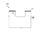
- FIG. 2 is a schematic view showing a part of the final silicon structure of the present embodiment.
- the silicon substrate W that is an object to be processed is a single crystal silicon substrate, but is not limited to this.
- the present embodiment can be applied even to a polycrystalline silicon substrate or an amorphous silicon substrate.
- the present embodiment can be applied to an object to be processed (for example, a substrate) having a polycrystalline silicon layer or an amorphous silicon layer in part.
- a silicon substrate W to be etched (hereinafter also simply referred to as a substrate W) is placed on a stage 21 provided on the lower side of the chamber 20.
- a gas selected from a first iodine fluoride gas that is an etching gas and a second iodine fluoride gas that is a protective film forming gas is supplied from each cylinder 22a and 22b, respectively. It is supplied through the regulators 23a and 23b. These gases are turned into plasma by the induction coil 24 to which high frequency power is applied by the first high frequency power source 25.
- high-frequency power is applied to the stage 21 using the second high-frequency power source 26, so that the generated plasma is drawn into the silicon substrate W.
- the power is applied to the stage 21 in a pulse form, in other words, in a state where the ON state and the OFF state of the application repeatedly appear at predetermined intervals.
- a vacuum pump 27 is connected to the chamber 20 via an exhaust flow rate regulator 28 in order to decompress the inside of the chamber 20 and exhaust a gas generated after the process. Note that the exhaust flow rate from the chamber 20 is changed by an exhaust flow rate regulator 28.
- the above-described gas flow rate regulators 23a and 23b, the first high frequency power source 25, the second high frequency power source 26 capable of applying pulses, and the exhaust flow rate regulator 28 are controlled by a control unit 29.
- a known pressure gauge for measuring the pressure in the chamber 20 is not shown.
- the manufacturing process of the silicon structure 10 of this embodiment will be described.
- the final silicon structure 10 of this embodiment has a trench structure having a width of about 50 ⁇ m and a depth of about 25 ⁇ m.
- Figure 3A is a diagram showing a time change of the flow rate of the embodiment of iodine pentafluoride in the protective film forming step pentafluoride in (IF 5) gas flow rate and the etching step (IF 5) gas.
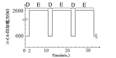
- FIG. 3B is a figure which shows the time change of the induction coil application electric power in the protective film formation process of this embodiment, and the induction coil application electric power in an etching process.
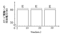
- FIG. 3C is a diagram showing temporal changes in power applied to the stage electrode (also referred to as substrate applied power) in the protective film forming step of the present embodiment and power applied to the stage electrode in the etching step.
- FIG. 3A is a diagram showing a time change of the flow rate of the embodiment of iodine pentafluoride in the protective film forming step pentafluoride in (IF 5) gas flow rate and the etching step (IF 5) gas.
- FIG. 3B is a figure which shows the time change of the induction
- 3D is a diagram illustrating a change over time in the chamber internal pressure in the protective film forming step and the chamber internal pressure in the etching step of the present embodiment.
- “D” representing the protective film forming step period
- “E” representing the etching step period are shown.
- 3A to 3D show only a part of the time zone of the repeated protective film forming process or etching process.
- the anisotropic dry etching of silicon includes a protective film forming step in which a second iodine fluoride gas that is a protective film forming gas is introduced, and a first iodine fluoride gas that is an etching gas.
- a method of sequentially repeating the introduced etching process is adopted.
- the protective film forming gas that is the first iodine fluoride gas and the etching gas that is the second iodine fluoride gas in this embodiment are both iodine pentafluoride (IF 5 ).
- a silicon substrate W on which a resist film is patterned as the etching mask 12 using a known photolithography technique is used.
- the protective film forming gas is 200 sccm (also referred to as 200 mL / min.) For 2 seconds which is one unit processing time.
- the pressure in the chamber 20 is controlled to 8 Pa.
- high frequency power of 13.56 MHz is applied to the induction coil 24 by 600 W (second high frequency power)
- no power is applied to the stage 21.
- the etching gas is supplied at 200 sccm for 9 seconds, which is a unit processing time, and the pressure in the chamber 20 is controlled to 15 Pa.
- a high frequency power of 13.56 MHz (first high frequency power) is applied to the induction coil 24, and a high frequency power of 13.56 MHz is 80 W to the stage 21 (a third high frequency power may be used for convenience).
- a third high frequency power may be used for convenience.
- the above-described protective film forming step and etching step are continuously repeated for a predetermined time (about 10 minutes in the present embodiment), whereby the silicon structure 10 shown in FIG. Is formed.
- the etching rate under the anisotropic dry etching conditions of this embodiment is about 2.5 ⁇ m / min. (Micrometers / minute).
- iodine pentafluoride IF 5
- GWP global warming potential
- the power to be applied to the induction coil 24 is set to a specific range, thereby to-be-processed object (for example, silicon substrate)
- the inventors' investigation confirmed that some deposits were formed on the surface of W). That is, by actively utilizing the above-described change in the form of the deposit due to the difference in applied power, as described above, even when only iodine pentafluoride (IF 5 ) gas is used, the protective film It is possible to create both a formation process and an etching process. Specifically, the applied power to the induction coil 24 in the protective film forming process is set lower than the applied power to the induction coil 24 in the etching process.
- a preferable coil applied power is 1000 W or more and 5000 W or less. If the coil applied power is less than 1000 W, the etching is hindered by the above-described deposits, so that there is a high possibility that a residue will form on the bottom surface of the etched structure such as a trench. On the other hand, when the coil applied power exceeds 5000 W, the manufacturing cost of the silicon structure increases including the cost required for the etching apparatus. Further, iodine pentafluoride case of plasma in the protective film forming step (IF 5) Gas, preferably coil applied power is less than 300 W 1000W.
- any of the above-mentioned deposits may be any substance containing I (iodine).
- the control unit 29 provided in the above-described manufacturing apparatus 100 is connected to the computer 60.
- the computer 60 monitors or comprehensively controls the above process by a manufacturing program of the silicon structure 10 for executing the above anisotropic dry etching process.
- a manufacturing program for the silicon structure 10 will be described with reference to a specific manufacturing flowchart.
- the above-described manufacturing program is stored in a known recording medium such as an optical disk inserted into a hard disk drive in the computer 60 or an optical disk drive provided in the computer 60.
- the storage destination of is not limited to this.
- the manufacturing program can also monitor or control each of the processes described above via a known technique such as a local area network or an Internet line.
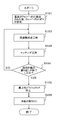
- FIG. 4 is a manufacturing flowchart of the silicon structure 10 of the present embodiment.
- step S101 after the silicon substrate W is transferred into the chamber 20, the gas in the chamber 20 is exhausted.
- steps S102 to S104 the silicon substrate W is subjected to anisotropic dry etching in the chamber 20 under the above-described conditions.
- step S102 a step of performing the protective film forming process of the present embodiment is executed.
- step S103 a step of performing the etching process of the present embodiment is executed.
- step S104 the program according to the present embodiment has the number of times that the respective steps of the step of performing the protective film forming step (step S102) and the step of performing the etching step (step S103) were initially set. It is determined whether or not it has been repeatedly executed. As a result, when the initially set number of times is repeatedly executed, the program of the present embodiment stops the anisotropic dry etching (step S105). On the other hand, when the initially set number of times is not repeatedly executed, a step of performing the protective film forming step and the etching step again is executed (steps S102 and S103).
- Step S106 the program of the present embodiment is brought into a state in which the silicon substrate W is taken out as shown in Step S105 (Step S106), and then the program of the present embodiment is finished.
- the substrate W may be directly taken out from the chamber after the chamber 20 is restored to the atmospheric pressure, but the substrate W is connected via a loader / unloader (not shown) device that can be connected to the chamber 20. May be removed.
- the manufacturing program for the silicon structure 10 of the present embodiment integrally controls each condition in the etching process and the protective film forming process as described above. As a result of executing the manufacturing program of the present embodiment, a silicon structure having a high sidewall and a good sidewall shape is formed.
- iodine pentafluoride IF 5
- the etching gas first iodine fluoride gas
- the protective film forming gas second iodine fluoride gas
- the present invention is not limited to this.
- iodine pentafluoride (IF 5 ) iodine trifluoride (IF 3 ) and iodine heptafluoride (IF 7 ) can also be applied to the above-described embodiments.
- the etching gas and the protective film forming gas need not be the same gas.
- the etching gas is iodine pentafluoride (IF 5 ) and the protective film forming gas is iodine trifluoride (IF 3 ), at least some of the effects of the above-described embodiment are achieved.
- an etching gas in which a plurality of types of iodine fluoride gas is mixed and a protective film forming gas in which a plurality of types of iodine fluoride gas are mixed can also be employed.
- the etching gas and the protective film forming gas are preferably the same.
- the object to be etched is a trench, but the present invention is not limited to this. Even if the object is a hole, substantially the same effect as the present invention can be obtained.
- the opening width is one type (50 ⁇ m), but the present invention is not limited to this. Even if there are two or more opening widths, the present invention can be applied.
- the protective film forming step is first performed, and then the etching step is performed.
- the order is not limited. For example, even if the etching process is performed first and then the protective film forming process is performed, the same effects as those of the above-described embodiment can be obtained.
- the protective film formation step first the protective film is deposited on the etching mask before being exposed to the plasma of the etching gas, which can contribute to improvement of the mask selectivity.
- the process immediately before stopping the anisotropic etching of the present embodiment is not limited to the etching process. Even if the protective film forming step is executed immediately before the anisotropic etching is stopped, the same effect as that of the present embodiment can be obtained.
- step S105 the program in which anisotropic etching is stopped (step S105) after step S102 is executed as a final process after steps S102 and S103 are repeated is also implemented. It can be applied as one variant of form.
- high-frequency power is applied to the stage electrode only in the etching process, but the present invention is not limited to this.
- high-frequency power can be applied to the stage electrode also in the protective film forming process. Since high-frequency power is applied in the protective film forming step, formation of the protective film on the bottom surface of the etched region may be suppressed, which may rather contribute to an improvement in the etching rate.
- ICP Inductively Coupled Plasma
- CCP Capacitive-Coupled Plasma
- ECR Electro-Cyclotron Resonance Plasma
Landscapes
- Engineering & Computer Science (AREA)
- Manufacturing & Machinery (AREA)
- Microelectronics & Electronic Packaging (AREA)
- Drying Of Semiconductors (AREA)
- Micromachines (AREA)
Abstract
本発明の1つのシリコン構造体の製造方法は、第1の高周波電力を印加することにより第1のフッ化ヨウ素をエッチングガスとしてプラズマ化する第1工程と、前述の第1の高周波電力よりも低い第2の高周波電力を印加することにより第2のフッ化ヨウ素を保護膜形成ガスとしてプラズマ化する第2工程とを交互に繰り返し行うことによって、シリコン領域を含む被処理物におけるそのシリコン領域をエッチングする工程とを有している。その結果、地球温暖化への影響を軽減したシリコンの異方性ドライエッチングによる、高い垂直性とともに良好な側壁形状を有するシリコン構造体が得られる。
Description
本発明は、シリコン構造体の製造方法及びその製造装置並びにその製造プログラムに関するものである。
シリコンを用いたMEMS(Micro Electro Mechanical Systems)デバイスが適用される技術分野は日進月歩で拡大しており、近年では、その技術がマイクロタービンやセンサーのみならず情報通信分野や医療分野へも適用されている。このMEMS技術を支える主要な要素技術の一つがシリコンの異方性ドライエッチングであり、この要素技術の発展がMEMS技術の発展を支えているといえる。
従来、幾つか存在するシリコンの異方性ドライエッチングプロセスの中で、本願出願人を含む複数の企業がこれまで提案してきた代表的なプロセスは、エッチング工程と保護膜形成工程とが繰り返し行われるプロセスである(例えば、特許文献1)。このプロセスのエッチング工程では、エッチングガスとして、主として六フッ化硫黄(SF6)が用いられてきた。また、このプロセスの保護膜形成工程では、保護膜形成ガスとして、有機系の堆積膜を形成する、主としてフッ化炭素(特に、C4F8)が用いられてきた。
近年、シリコンの異方性ドライエッチングの技術は飛躍的に進歩してきたが、その一方で、これまでそのプロセスを実施するために産業界で使用されてきた温室効果ガスの影響が懸念され始めている。例えば、上述の六フッ化硫黄(SF6)やC4F8に代表されるフッ化炭素は、いわゆる地球温暖化係数(GWP)が非常に高いため、このガスに代替するガスを見出し、市場に送り出すことは、地球環境を考える上でも急務であるといえる。しかしながら、六フッ化硫黄(SF6)やフッ化炭素は、これまでシリコンの異方性ドライエッチング技術を支える基幹ガスとして用いられてきたため、市場の要求に耐えうる代替ガスを見出すことは容易ではない。
本発明は、六フッ化硫黄(SF6)やフッ化炭素に代わる温暖化係数の低いガスを用いて高い垂直性と良好な側壁形状を達成する、シリコンの異方性ドライエッチング技術の発展に大いに貢献するものである。
発明者らは、六フッ化硫黄(SF6)及びフッ化炭素の代替ガスを選定するにあたり、六フッ化硫黄(SF6)のプラズマ化によるシリコンのエッチング特性及びフッ化炭素のプラズマ化によるシリコン上に形成される保護膜の特性の調査分析を行った。加えて、発明者らは、特に各種デバイスの性能に直接影響する、シリコン構造体の異方性及び側壁の形状に着目し、数多くの代替ガスの候補について鋭意研究を行った。その結果、発明者らは、地球温暖化係数(GWP)が殆ど無視できるほどに小さいガスが、条件によってはそのガス単体であっても、上述のエッチング工程と保護膜形成工程とが繰り返し行われるプロセスに適用し得ることを見出した。
具体的には、未だ詳しいメカニズムは判明していないが、上述のガスを採用した場合、プラズマ化させる際に印加する電力を特定の範囲に設定することによって、被処理物(例えば、シリコン基板)の表面上に何らかの堆積物が形成され易いことが確認された。そこで発明者らは、上述の印加電力の差による堆積物の態様の変化を積極的に利用することにより、六フッ化硫黄(SF6)のみならず、地球温暖化係数(GWP)の高い保護膜形成のためのフッ化炭素ガスを使用することなく、シリコンの異方性エッチングが可能となることを見出した。本発明は上述の視点により創出された。
本発明の1つのシリコン構造体の製造方法は、第1の高周波電力を印加することにより第1のフッ化ヨウ素をエッチングガスとしてプラズマ化する第1工程と、前述の第1の高周波電力よりも低い第2の高周波電力を印加することにより第2のフッ化ヨウ素を保護膜形成ガスとしてプラズマ化する第2工程とを交互に繰り返し行うことによって、シリコン領域を含む被処理物におけるそのシリコン領域をエッチングする工程を有している。
このシリコン構造体の製造方法によれば、第1のフッ化ヨウ素が六フッ化硫黄(SF6)に代わって用いられるだけでなく、従来保護膜形成ガスとして用いられてきたC4F8に代表されるフッ化炭素ガスも使用されない。その結果、第1のフッ化ヨウ素がプラズマ化されるエッチング工程と第2のフッ化ヨウ素がプラズマ化される保護膜形成工程とが交互に繰り返し行われるプロセスにより、高い垂直性と良好な側壁形状を有するシリコン構造体が得られる。
また、本発明のもう1つのシリコン構造体の製造方法は、誘電結合型プラズマエッチング装置を用いて誘導コイル(以下、単にコイルとも言う。)に第1の高周波電力を印加することにより第1のフッ化ヨウ素をエッチングガスとしてプラズマ化する第1工程と、その誘導コイルに前述の第1の高周波電力よりも低い第2の高周波電力を印加することにより第2のフッ化ヨウ素を保護膜形成ガスとしてプラズマ化する第2工程とを交互に繰り返し行うとともに、前述の第1工程の間、シリコン領域を含む被処理物が載置されるステージ電極に高周波電力を印加することによって、そのシリコン領域をエッチングする工程を有している。
このシリコン構造体の製造方法によれば、第1のフッ化ヨウ素が六フッ化硫黄(SF6)に代わって用いられるだけでなく、従来保護膜形成ガスとして用いられてきたC4F8に代表されるフッ化炭素ガスも使用されない。その結果、第1のフッ化ヨウ素が誘電結合型プラズマエッチング装置によってプラズマ化されるエッチング工程とその装置によって第2のフッ化ヨウ素がプラズマ化される保護膜形成工程とが交互に繰り返し行われるプロセスにより、高い垂直性と良好な側壁形状を有するシリコン構造体が得られる。
また、本発明の1つのシリコン構造体の製造プログラムは、第1の高周波電力を印加することにより第1のフッ化ヨウ素をエッチングガスとしてプラズマ化する第1ステップと、前述の第1の高周波電力よりも低い第2の高周波電力を印加することにより第2のフッ化ヨウ素を保護膜形成ガスとしてプラズマ化する第2ステップとを交互に繰り返し行うことによって、シリコン領域を含む被処理物におけるそのシリコン領域をエッチングするステップを有している。
このシリコン構造体の製造プログラムによれば、第1のフッ化ヨウ素が六フッ化硫黄(SF6)に代わって用いられるだけでなく、従来保護膜形成ガスとして用いられてきたC4F8に代表されるフッ化炭素ガスも使用されない。その結果、第1のフッ化ヨウ素がプラズマ化されるエッチングステップと第2のフッ化ヨウ素がプラズマ化される保護膜形成ステップとが交互に繰り返し行われることにより、高い垂直性と良好な側壁形状を有するシリコン構造体が得られる。
また、本発明のもう1つのシリコン構造体の製造プログラムは、誘電結合型プラズマエッチング装置を用いて誘導コイルに第1の高周波電力を印加することにより第1のフッ化ヨウ素をエッチングガスとしてプラズマ化する第1ステップと、その誘導コイルに前述の第1の高周波電力よりも低い第2の高周波電力を印加することにより第2のフッ化ヨウ素を保護膜形成ガスとしてプラズマ化する第2ステップとを交互に繰り返し行うとともに、前述の第1ステップの間、シリコン領域を含む被処理物が載置されるステージ電極に高周波電力を印加することによって、そのシリコン領域をエッチングするステップを有している。
このシリコン構造体の製造プログラムによれば、第1のフッ化ヨウ素が六フッ化硫黄(SF6)に代わって用いられるだけでなく、従来保護膜形成ガスとして用いられてきたC4F8に代表されるフッ化炭素ガスも使用されない。その結果、第1のフッ化ヨウ素が誘電結合型プラズマエッチング装置によってプラズマ化されるエッチングステップとその装置によって第2のフッ化ヨウ素がプラズマ化される保護膜形成ステップとが交互に繰り返し行われることにより、高い垂直性と良好な側壁形状を有するシリコン構造体が得られる。
また、本発明の1つのシリコン構造体の製造装置は、上述のいずれかのシリコン構造体の製造プログラム又はそのいずれかのシリコン構造体の製造プログラムを記録した記録媒体によって制御される制御部を備えている。
本発明の製造方法、製造装置、又は製造プログラムによれば、第1のフッ化ヨウ素がプラズマ化されるエッチング工程と第2のフッ化ヨウ素がプラズマ化される保護膜形成工程とが交互に繰り返し行われることにより、高い垂直性と良好な側壁形状を有するシリコン構造体が得られる。また、フッ化ヨウ素は、地球温暖化係数(GWP)が高い六フッ化硫黄(SF6)やフッ化炭素ガス(代表的には、C4F8)と比較して殆ど無視できるほどに小さいガス(実質的に、GWPが0(ゼロ))であることから、地球温暖化抑制にも大きく貢献し得る。
10 シリコン構造体
12 エッチングマスク
14 側壁
20 チャンバー
21 ステージ
22a,22b ガスボンベ
23a,23b ガス流量調整器
24 誘導コイル
25 第1高周波電源
26 第2高周波電源
27 真空ポンプ
28 排気流量調整器
29 制御部
60 コンピュータ
100 シリコン構造体の製造装置
12 エッチングマスク
14 側壁
20 チャンバー
21 ステージ
22a,22b ガスボンベ
23a,23b ガス流量調整器
24 誘導コイル
25 第1高周波電源
26 第2高周波電源
27 真空ポンプ
28 排気流量調整器
29 制御部
60 コンピュータ
100 シリコン構造体の製造装置
つぎに、本発明の実施形態を、添付する図面に基づいて詳細に述べる。尚、この説明に際し、全図にわたり、特に言及がない限り、共通する部分には共通する参照符号が付されている。また、図中、本実施形態の要素は必ずしもスケール通りに示されていない。また、各図面を見やすくするために、一部の符号が省略され得る。また、特に言及がない限り、以下の各種ガスの流量は、標準状態の流量を示す。
図1は、本実施形態のシリコン構造体の製造装置100(以下、単に製造装置100ともいう)の装置構成の一例を示す断面図である。また、図2は、本実施形態の最終的なシリコン構造体の一部を示す模式図である。なお、本実施形態において、被処理物であるシリコン基板Wは単結晶シリコン基板であるが、これに限定されない。例えば、多結晶シリコン基板やアモルファスシリコン基板であっても本実施形態は適用され得る。同様に、多結晶シリコン層やアモルファスシリコン層を一部に有する被処理物(例えば、基板)に対しても本実施形態は適用され得る。
まず、図1に示すシリコン構造体の製造装置100の構成について説明する。エッチング対象となるシリコン基板W(以下、単に基板Wともいう。)は、チャンバー20の下部側に設けられたステージ21に載置される。チャンバー20には、エッチングガスである第1のフッ化ヨウ素ガス、及び保護膜形成ガスである第2のフッ化ヨウ素ガスから選ばれる少なくとも一種類のガスが、各ボンベ22a,22bからそれぞれガス流量調整器23a,23bを通して供給される。これらのガスは、第1高周波電源25により高周波電力を印加された誘導コイル24によりプラズマ化される。その後、第2高周波電源26を用いてステージ21に高周波電力が印加されることにより、これらの生成されたプラズマはシリコン基板Wに引き込まれる。ここで、本実施形態では、ステージ21に対してパルス状、換言すれば、印加のオン状態とオフ状態が所定間隔で繰り返し現れる状況で電力が印加される。また、このチャンバー20内を減圧し、かつプロセス後に生成されるガスを排気するため、チャンバー20には真空ポンプ27が排気流量調整器28を介して接続されている。なお、このチャンバー20からの排気流量は排気流量調整器28により変更される。上述のガス流量調整器23a,23b、第1高周波電源25、パルス状の印加が可能な第2高周波電源26、及び排気流量調整器28は、制御部29により制御される。また、チャンバー20内の圧力を計測する公知の圧力計は図示されていない。
次に、本実施形態のシリコン構造体10の製造工程について説明する。なお、本実施形態の最終的なシリコン構造体10は、幅が約50μmであって深さが約25μmのトレンチ構造を備えている。
図3Aは、本実施形態の保護膜形成工程における五フッ化ヨウ素(IF5)ガスの流量及びエッチング工程における五フッ化ヨウ素(IF5)ガスの流量の時間変化を示す図である。また、図3Bは、本実施形態の保護膜形成工程における誘導コイル印加電力及びエッチング工程における誘導コイル印加電力の時間変化を示す図である。また、図3Cは、本実施形態の保護膜形成工程におけるステージ電極への印加電力(基板印加電力とも言う)及びエッチング工程におけるステージ電極への印加電力の時間変化を示す図である。加えて、図3Dは、本実施形態の保護膜形成工程におけるチャンバー内圧力及びエッチング工程におけるチャンバー内圧力の時間変化を示す図である。なお、各図中における保護膜形成工程とエッチング工程とを判別し易くするために、保護膜形成工程期間を表す「D」と、エッチング工程期間を表す「E」が示されている。また、図3A乃至図3Dは、言うまでもなく、繰り返される保護膜形成工程又はエッチング工程の一部の時間帯のみを示している。
ここで、本実施形態のシリコンの異方性ドライエッチングは、保護膜形成ガスである第2のフッ化ヨウ素ガスが導入される保護膜形成工程とエッチングガスである第1のフッ化ヨウ素ガスが導入されるエッチング工程とを順次繰り返す方法を採用する。本実施形態の第1のフッ化ヨウ素ガスである保護膜形成ガスと第2のフッ化ヨウ素ガスであるエッチングガスは、ともに五フッ化ヨウ素(IF5)である。なお、本実施形態では、公知のフォトリソグラフィー技術を用いてエッチングマスク12としてのレジスト膜のパターニングがなされたシリコン基板Wが用いられる。
本実施形態のシリコン構造体10の製造工程では、最初に、保護膜形成工程において、一単位処理時間である2秒間に、保護膜形成ガスが200sccm(200mL/min.ともいう。以下の各流量において同じ。)で供給され、チャンバー20内の圧力は8Paに制御される。誘導コイル24には、13.56MHzの高周波電力が600W(第2の高周波電力)印加されるが、ステージ21には電力が印加されない。一方、つづくエッチング工程では、一単位処理時間である9秒間に、エッチングガスが200sccmで供給され、チャンバー20内の圧力は15Paに制御される。誘導コイル24には13.56MHzの高周波電力が2600W(第1の高周波電力)印加されるとともに、ステージ21には13.56MHzの高周波電力が80W(便宜上、第3の高周波電力としても良い。)印加される。図3A乃至図3Dに示すように、上述の保護膜形成工程及びエッチング工程が、所定の時間(本実施形態では約10分間)、継続して繰り返されることにより、図2に示すシリコン構造体10が形成される。
なお、本実施形態の異方性ドライエッチング条件によるエッチング速度は、約2.5μm/min.(マイクロメートル/分)である。
上述のとおり、本実施形態では、保護膜形成工程及びエッチング工程において、地球温暖化係数(GWP)が殆ど無視できるほどに小さい五フッ化ヨウ素(IF5)が用いられている。従って、上述のとおり、図2に示すトレンチ構造を有するシリコン構造体10の形成のために排出される温室効果ガスの総量は顕著に抑制される。
未だ詳しいメカニズムは判明していないが、上述の五フッ化ヨウ素(IF5)を採用した場合、誘導コイル24への印加電力を特定の範囲に設定することによって、被処理物(例えば、シリコン基板W)の表面上に何らかの堆積物が形成されることが発明者らの調査によって確認された。すなわち、上述の印加電力の差による堆積物の態様の変化を積極的に利用することにより、上述のように、五フッ化ヨウ素(IF5)ガスのみを用いた場合であっても、保護膜形成工程とエッチング工程の両方を創り出すことが可能となる。具体的には、エッチング工程における誘導コイル24への印加電力よりも、保護膜形成工程における誘導コイル24への印加電力が低く設定される。
ここで、五フッ化ヨウ素(IF5)ガスをエッチング工程でプラズマ化する場合、好ましいコイル印加電力は、1000W以上5000W以下である。このコイル印加電力が、1000W未満になれば、上述の堆積物によってエッチングが阻害されることにより、エッチングされたトレンチ等の構造の底面に残渣が生じる可能性が高くなる。一方、このコイル印加電力が、5000Wを超えると、エッチング装置に要する費用を含めてシリコン構造体の製造コストが上昇するためである。また、五フッ化ヨウ素(IF5)ガスを保護膜形成工程においてプラズマ化する場合、好ましいコイル印加電力は、300W以上1000W未満である。このコイル印加電力が300W未満になれば、五フッ化ヨウ素(IF5)ガスのプラズマ化が達成されない可能性が高まる。一方、このコイル印加電力が1000W以上になると、堆積物の生成よりもシリコンのエッチングに寄与してしまうためである。なお、発明者らによる分析の結果、現段階では、上述の何らかの堆積物は、I(ヨウ素)を含んだ何らかの物質であろうと考えられる。
ところで、上述の製造装置100に備えられている制御部29は、コンピュータ60に接続されている。コンピュータ60は、上述の異方性ドライエッチングプロセスを実行するためのシリコン構造体10の製造プログラムにより、上述のプロセスを監視し、又は統合的に制御する。以下に、具体的な製造フローチャートを示しながら、シリコン構造体10の製造プログラムを説明する。尚、本実施形態では、上述の製造プログラムがコンピュータ60内のハードディスクドライブ、又はコンピュータ60に設けられた光ディスクドライブ等に挿入される光ディスク等の公知の記録媒体に保存されているが、この製造プログラムの保存先はこれに限定されない。また、この製造プログラムは、ローカルエリアネットワークやインターネット回線等の公知の技術を介して上述の各プロセスを監視し、又は制御することもできる。
図4は、本実施形態のシリコン構造体10の製造フローチャートである。
図4に示すとおり、本実施形態のシリコン構造体10の製造プログラムが実行されると、まず、ステップS101において、シリコン基板Wがチャンバー20内に搬送された後、チャンバー20内のガスが排気される。その後、ステップS102~ステップS104において、チャンバー20内でシリコン基板Wが既述の条件により異方性ドライエッチングが行われる。
具体的には、まず、ステップS102において、本実施形態の保護膜形成工程を行うステップが実行される。次に、本実施形態のエッチング工程を行うステップが実行される(ステップS103)。
その後、本実施形態のプログラムは、ステップS104に示すように、上述の保護膜形成工程を行うステップ(ステップS102)とエッチング工程を行うステップ(ステップS103)の各工程を当初設定されていた回数が繰り返して実行されたか否かを判断する。その結果、当初設定されていた回数が繰り返して実行された場合は、本実施形態のプログラムは異方性ドライエッチングを停止する(ステップS105)。他方、当初設定されていた回数が繰り返して実行されていない場合は、保護膜形成工程及びエッチング工程を再度行うステップが実行される(ステップS102,ステップS103)。
異方性ドライエッチングが停止した後、本実施形態のプログラムは、ステップS105に示すように、シリコン基板Wが取り出される状態にし(ステップS106)、その後、本実施形態のプログラムが終了する。なお、このとき、チャンバー20が大気圧に回復した後にチャンバー内から直接基板Wが取り出されても良いが、チャンバー20に接続し得るローダー/アンローダー(図示されていない)装置を介して基板Wが取り出されてもよい。
本実施形態のシリコン構造体10の製造プログラムは、上述のとおり、エッチング工程及び保護膜形成工程における各条件等を統合的に制御する。本実施形態の製造プログラムが実行される結果、高い垂直性とともに良好な側壁形状を有するシリコン構造体が形成される。
ところで、上述の実施形態では、エッチングガス(第1のフッ化ヨウ素ガス)及び保護膜形成ガス(第2のフッ化ヨウ素ガス)のいずれも五フッ化ヨウ素(IF5)が用いられているが、これに限定されない。五フッ化ヨウ素(IF5)の代わりに三フッ化ヨウ素(IF3)や七フッ化ヨウ素(IF7)も上述の実施形態に適用され得る。また、エッチングガスと保護膜形成ガスとが同一のガスである必要はない。例えば、エッチングガスが五フッ化ヨウ素(IF5)であって、保護膜形成ガスが三フッ化ヨウ素(IF3)であっても、上述の実施形態の少なくとも一部の効果が奏される。加えて、複数種のフッ化ヨウ素ガスが混合されたエッチングガスや、複数種のフッ化ヨウ素ガスが混合された保護膜形成ガスも採用され得る。但し、プロセスの管理ないし排気ガスの管理の容易性の観点から言えば、エッチングガスと保護膜形成ガスとが同じであることが好ましい。
また、上述の実施形態では、エッチングされる対象がトレンチであったが、これに限定されない。その対象がホールであっても、本発明と実質的に同様の効果が奏される。さらに、上述の実施形態では、開口幅が1種類(50μm)であったが、これに限定されない。仮に、開口幅が2種類以上であっても本発明を適用することができる。
また、上述の実施形態では、まず保護膜形成工程が行われ、その後にエッチング工程が行われたが、この順序に限定されない。例えば、最初にエッチング工程が行われ、その後に保護膜形成工程が行われても上述の実施形態とほぼ同様の効果が奏される。但し、保護膜形成工程を最初に行うことにより、エッチングガスのプラズマに曝露される前にエッチングマスク上に保護膜が堆積することになるため、マスク選択比の向上に寄与しうる。また、本実施形態の異方性エッチングを停止する直前の工程がエッチング工程に限定されることもない。保護膜形成工程が異方性エッチングを停止する直前に実行されても本実施形態の効果と同様の効果が奏される。すなわち、図4で示すフローチャートに基づけば、ステップS102とステップS103とが繰り返された上で、最終工程としてステップS102が実行された後に、異方性エッチングが停止(ステップS105)するプログラムも本実施形態の1つの変形例として適用され得る。
また、上述の実施形態では、エッチング工程においてのみ、ステージ電極へ高周波電力が印加されているが、これに限定されない。例えば、エッチング工程に加えて、保護膜形成工程においてもステージ電極に対して高周波電力が印加され得る。保護膜形成工程において高周波電力が印加されることにより、エッチングされた領域の底面の保護膜の形成を抑制する場合があるため、むしろエッチング速度の向上に寄与し得る。
さらに、プラズマ生成手段として上述の実施形態ではICP(Inductively Coupled Plasma)を用いたが、本発明はこれに限定されない。他の高密度プラズマ、例えば、CCP(Capacitive-Coupled Plasma)やECR(Electron-Cyclotron Resonance Plasma)を用いても上述の実施形態の効果と同様の効果が奏され得る。以上、述べたとおり、本発明の範囲内に存在する変形例もまた、特許請求の範囲に含まれるものである。
Claims (11)
- 第1の高周波電力を印加することにより第1のフッ化ヨウ素をエッチングガスとしてプラズマ化する第1工程と、前記第1の高周波電力よりも低い第2の高周波電力を印加することにより第2のフッ化ヨウ素を保護膜形成ガスとしてプラズマ化する第2工程とを交互に繰り返し行うことによって、シリコン領域を含む被処理物の前記シリコン領域をエッチングする工程を有する
シリコン構造体の製造方法。 - 誘電結合型プラズマエッチング装置を用いて誘導コイルに第1の高周波電力を印加することにより第1のフッ化ヨウ素をエッチングガスとしてプラズマ化する第1工程と、前記誘導コイルに前記第1の高周波電力よりも低い第2の高周波電力を印加することにより第2のフッ化ヨウ素を保護膜形成ガスとしてプラズマ化する第2工程とを交互に繰り返し行うとともに、前記第1工程の間、シリコン領域を含む被処理物が載置されるステージ電極に高周波電力を印加することによって、前記シリコン領域をエッチングする工程を有する
シリコン構造体の製造方法。 - 前記第1のフッ化ヨウ素及び前記第2のフッ化ヨウ素が、五フッ化ヨウ素(IF5)である
請求項1又は請求項2に記載のシリコン構造体の製造方法。 - 前記第1の高周波電力は、1000W以上5000W以下であり、前記第2の高周波電力は、300W以上1000W未満である
請求項1又は請求項2に記載のシリコン構造体の製造方法。 - 第1の高周波電力を印加することにより第1のフッ化ヨウ素をエッチングガスとしてプラズマ化する第1ステップと、前記第1の高周波電力よりも低い第2の高周波電力を印加することにより第2のフッ化ヨウ素を保護膜形成ガスとしてプラズマ化する第2ステップとを交互に繰り返し行うことによって、シリコン領域を含む被処理物の前記シリコン領域をエッチングするステップを有する
シリコン構造体の製造プログラム。 - 誘電結合型プラズマエッチング装置を用いて誘導コイルに第1の高周波電力を印加することにより第1のフッ化ヨウ素をエッチングガスとしてプラズマ化する第1ステップと、前記誘導コイルに前記第1の高周波電力よりも低い第2の高周波電力を印加することにより第2のフッ化ヨウ素を保護膜形成ガスとしてプラズマ化する第2ステップとを交互に繰り返し行うとともに、前記第1ステップの間、シリコン領域を含む被処理物が載置されるステージ電極に高周波電力を印加することによって、前記シリコン領域をエッチングするステップを有する
シリコン構造体の製造プログラム。 - 前記第1のフッ化ヨウ素及び前記第2のフッ化ヨウ素が、五フッ化ヨウ素(IF5)である
請求項5又は請求項6に記載のシリコン構造体の製造プログラム。 - 前記第1の高周波電力は、1000W以上5000W以下であり、前記第2の高周波電力は、300W以上1000W未満である
請求項5又は請求項6に記載のシリコン構造体の製造プログラム。 - 請求項5又は請求項6に記載の製造プログラムを記録した記録媒体。
- 請求項5又は請求項6に記載の製造プログラムにより制御される制御部を備えた
シリコン構造体の製造装置。 - 請求項9に記載の記録媒体により制御される制御部を備えた
シリコン構造体の製造装置。
Priority Applications (1)
| Application Number | Priority Date | Filing Date | Title |
|---|---|---|---|
| JP2011520843A JP5749166B2 (ja) | 2009-07-01 | 2010-06-02 | シリコン構造体の製造方法及びその製造装置並びにその製造プログラム |
Applications Claiming Priority (2)
| Application Number | Priority Date | Filing Date | Title |
|---|---|---|---|
| JP2009-157061 | 2009-07-01 | ||
| JP2009157061 | 2009-07-01 |
Publications (1)
| Publication Number | Publication Date |
|---|---|
| WO2011001779A1 true WO2011001779A1 (ja) | 2011-01-06 |
Family
ID=43410859
Family Applications (1)
| Application Number | Title | Priority Date | Filing Date |
|---|---|---|---|
| PCT/JP2010/059344 Ceased WO2011001779A1 (ja) | 2009-07-01 | 2010-06-02 | シリコン構造体の製造方法及びその製造装置並びにその製造プログラム |
Country Status (3)
| Country | Link |
|---|---|
| JP (1) | JP5749166B2 (ja) |
| TW (1) | TW201103088A (ja) |
| WO (1) | WO2011001779A1 (ja) |
Cited By (1)
| Publication number | Priority date | Publication date | Assignee | Title |
|---|---|---|---|---|
| JP2014007350A (ja) * | 2012-06-27 | 2014-01-16 | Nippon Dempa Kogyo Co Ltd | エッチング方法及びmemsデバイス |
Families Citing this family (2)
| Publication number | Priority date | Publication date | Assignee | Title |
|---|---|---|---|---|
| CN102737983B (zh) * | 2012-07-05 | 2015-06-17 | 中微半导体设备(上海)有限公司 | 半导体结构的形成方法 |
| CN102737984B (zh) * | 2012-07-06 | 2015-08-05 | 中微半导体设备(上海)有限公司 | 半导体结构的形成方法 |
Citations (1)
| Publication number | Priority date | Publication date | Assignee | Title |
|---|---|---|---|---|
| JP2008177209A (ja) * | 2007-01-16 | 2008-07-31 | Taiyo Nippon Sanso Corp | プラズマエッチング方法 |
Family Cites Families (1)
| Publication number | Priority date | Publication date | Assignee | Title |
|---|---|---|---|---|
| JP4209774B2 (ja) * | 2001-09-28 | 2009-01-14 | 住友精密工業株式会社 | シリコン基板のエッチング方法およびエッチング装置 |
-
2010
- 2010-06-02 JP JP2011520843A patent/JP5749166B2/ja active Active
- 2010-06-02 WO PCT/JP2010/059344 patent/WO2011001779A1/ja not_active Ceased
- 2010-06-29 TW TW099121307A patent/TW201103088A/zh unknown
Patent Citations (1)
| Publication number | Priority date | Publication date | Assignee | Title |
|---|---|---|---|---|
| JP2008177209A (ja) * | 2007-01-16 | 2008-07-31 | Taiyo Nippon Sanso Corp | プラズマエッチング方法 |
Cited By (1)
| Publication number | Priority date | Publication date | Assignee | Title |
|---|---|---|---|---|
| JP2014007350A (ja) * | 2012-06-27 | 2014-01-16 | Nippon Dempa Kogyo Co Ltd | エッチング方法及びmemsデバイス |
Also Published As
| Publication number | Publication date |
|---|---|
| JP5749166B2 (ja) | 2015-07-15 |
| TW201103088A (en) | 2011-01-16 |
| JPWO2011001779A1 (ja) | 2012-12-13 |
Similar Documents
| Publication | Publication Date | Title |
|---|---|---|
| KR20090091307A (ko) | 높은 아스펙트비의 개구를 갖는 실리콘 구조체, 이의 제조방법, 이의 제조 장치, 및 이의 제조 프로그램, 및 이의 실리콘 구조체용 에칭 마스크의 제조방법 | |
| JP5308080B2 (ja) | シリコン構造体の製造方法及びその製造装置並びにその製造プログラム | |
| WO2018180663A1 (ja) | プラズマ処理方法 | |
| JP2009206401A (ja) | プラズマエッチング方法、プラズマエッチング装置及びコンピュータ記憶媒体 | |
| JP5203340B2 (ja) | 半導体装置の製造方法 | |
| KR102267521B1 (ko) | 에칭 방법 | |
| JP5749166B2 (ja) | シリコン構造体の製造方法及びその製造装置並びにその製造プログラム | |
| Osipov et al. | OES diagnostics as a universal technique to control the Si etching structures profile in ICP | |
| JP6183965B2 (ja) | シリコン酸化膜及びその製造方法、並びにシリコン酸化膜の製造装置 | |
| WO2011001778A1 (ja) | シリコン構造体の製造方法及びその製造装置並びにその製造プログラム | |
| JP5172417B2 (ja) | シリコン構造体の製造方法及びその製造装置並びにその製造プログラム | |
| US7205226B1 (en) | Sacrificial layer for protection during trench etch | |
| JP5065726B2 (ja) | ドライエッチング方法 | |
| US8709952B2 (en) | Etching method, etching apparatus, and computer-readable recording medium | |
| Rui et al. | Applications and mechanisms of anisotropic two-step Si3N4 etching with hydrogen plasma conditioning | |
| JP5074009B2 (ja) | 高アスペクト比の開口を有するシリコン構造体用エッチングマスクの製造方法及びその装置並びにその製造プログラム | |
| JP5443937B2 (ja) | シリコン構造体の製造方法及びその製造装置並びにその製造プログラム | |
| JP5284679B2 (ja) | プラズマエッチング方法 | |
| JP5177997B2 (ja) | 高アスペクト比の開口を有するシリコン構造体、その製造方法、その製造装置、及びその製造プログラム | |
| JP2009147000A (ja) | 半導体装置の製造方法 | |
| JP5416540B2 (ja) | シリコン構造体の製造方法及びその製造装置並びにその製造プログラム | |
| US10937662B2 (en) | Method of isotropic etching of silicon oxide utilizing fluorocarbon chemistry | |
| JP4700922B2 (ja) | 半導体装置の製造方法 | |
| JP6225005B2 (ja) | 積層膜及びその製造方法 | |
| JP4958658B2 (ja) | プラズマ処理方法 |
Legal Events
| Date | Code | Title | Description |
|---|---|---|---|
| 121 | Ep: the epo has been informed by wipo that ep was designated in this application |
Ref document number: 10793950 Country of ref document: EP Kind code of ref document: A1 |
|
| WWE | Wipo information: entry into national phase |
Ref document number: 2011520843 Country of ref document: JP |
|
| NENP | Non-entry into the national phase |
Ref country code: DE |
|
| 122 | Ep: pct application non-entry in european phase |
Ref document number: 10793950 Country of ref document: EP Kind code of ref document: A1 |