WO2010150407A1 - 半導体装置 - Google Patents
半導体装置 Download PDFInfo
- Publication number
- WO2010150407A1 WO2010150407A1 PCT/JP2009/061769 JP2009061769W WO2010150407A1 WO 2010150407 A1 WO2010150407 A1 WO 2010150407A1 JP 2009061769 W JP2009061769 W JP 2009061769W WO 2010150407 A1 WO2010150407 A1 WO 2010150407A1
- Authority
- WO
- WIPO (PCT)
- Prior art keywords
- channel region
- insulating film
- semiconductor device
- regions
- channel
- Prior art date
- Legal status (The legal status is an assumption and is not a legal conclusion. Google has not performed a legal analysis and makes no representation as to the accuracy of the status listed.)
- Ceased
Links
Images









Classifications
-
- H—ELECTRICITY
- H10—SEMICONDUCTOR DEVICES; ELECTRIC SOLID-STATE DEVICES NOT OTHERWISE PROVIDED FOR
- H10D—INORGANIC ELECTRIC SEMICONDUCTOR DEVICES
- H10D86/00—Integrated devices formed in or on insulating or conducting substrates, e.g. formed in silicon-on-insulator [SOI] substrates or on stainless steel or glass substrates
- H10D86/01—Manufacture or treatment
-
- G—PHYSICS
- G11—INFORMATION STORAGE
- G11C—STATIC STORES
- G11C11/00—Digital stores characterised by the use of particular electric or magnetic storage elements; Storage elements therefor
- G11C11/21—Digital stores characterised by the use of particular electric or magnetic storage elements; Storage elements therefor using electric elements
- G11C11/34—Digital stores characterised by the use of particular electric or magnetic storage elements; Storage elements therefor using electric elements using semiconductor devices
- G11C11/39—Digital stores characterised by the use of particular electric or magnetic storage elements; Storage elements therefor using electric elements using semiconductor devices using thyristors or the avalanche or negative resistance type, e.g. PNPN, SCR, SCS, UJT
-
- H—ELECTRICITY
- H10—SEMICONDUCTOR DEVICES; ELECTRIC SOLID-STATE DEVICES NOT OTHERWISE PROVIDED FOR
- H10B—ELECTRONIC MEMORY DEVICES
- H10B10/00—Static random access memory [SRAM] devices
-
- H—ELECTRICITY
- H10—SEMICONDUCTOR DEVICES; ELECTRIC SOLID-STATE DEVICES NOT OTHERWISE PROVIDED FOR
- H10D—INORGANIC ELECTRIC SEMICONDUCTOR DEVICES
- H10D30/00—Field-effect transistors [FET]
-
- H—ELECTRICITY
- H10—SEMICONDUCTOR DEVICES; ELECTRIC SOLID-STATE DEVICES NOT OTHERWISE PROVIDED FOR
- H10D—INORGANIC ELECTRIC SEMICONDUCTOR DEVICES
- H10D30/00—Field-effect transistors [FET]
- H10D30/60—Insulated-gate field-effect transistors [IGFET]
- H10D30/62—Fin field-effect transistors [FinFET]
-
- H—ELECTRICITY
- H10—SEMICONDUCTOR DEVICES; ELECTRIC SOLID-STATE DEVICES NOT OTHERWISE PROVIDED FOR
- H10D—INORGANIC ELECTRIC SEMICONDUCTOR DEVICES
- H10D30/00—Field-effect transistors [FET]
- H10D30/60—Insulated-gate field-effect transistors [IGFET]
- H10D30/67—Thin-film transistors [TFT]
- H10D30/6757—Thin-film transistors [TFT] characterised by the structure of the channel, e.g. transverse or longitudinal shape or doping profile
-
- H—ELECTRICITY
- H10—SEMICONDUCTOR DEVICES; ELECTRIC SOLID-STATE DEVICES NOT OTHERWISE PROVIDED FOR
- H10D—INORGANIC ELECTRIC SEMICONDUCTOR DEVICES
- H10D48/00—Individual devices not covered by groups H10D1/00 - H10D44/00
- H10D48/383—Quantum effect devices, e.g. of devices using quantum reflection, diffraction or interference effects
- H10D48/3835—Semiconductor qubit devices comprising a plurality of quantum mechanically interacting semiconductor quantum dots, e.g. Loss-DiVincenzo spin qubits
-
- H—ELECTRICITY
- H10—SEMICONDUCTOR DEVICES; ELECTRIC SOLID-STATE DEVICES NOT OTHERWISE PROVIDED FOR
- H10D—INORGANIC ELECTRIC SEMICONDUCTOR DEVICES
- H10D8/00—Diodes
- H10D8/70—Tunnel-effect diodes
- H10D8/755—Resonant tunneling diodes [RTD]
-
- H—ELECTRICITY
- H10—SEMICONDUCTOR DEVICES; ELECTRIC SOLID-STATE DEVICES NOT OTHERWISE PROVIDED FOR
- H10D—INORGANIC ELECTRIC SEMICONDUCTOR DEVICES
- H10D86/00—Integrated devices formed in or on insulating or conducting substrates, e.g. formed in silicon-on-insulator [SOI] substrates or on stainless steel or glass substrates
- H10D86/201—Integrated devices formed in or on insulating or conducting substrates, e.g. formed in silicon-on-insulator [SOI] substrates or on stainless steel or glass substrates the substrates comprising an insulating layer on a semiconductor body, e.g. SOI
-
- H—ELECTRICITY
- H10—SEMICONDUCTOR DEVICES; ELECTRIC SOLID-STATE DEVICES NOT OTHERWISE PROVIDED FOR
- H10B—ELECTRONIC MEMORY DEVICES
- H10B12/00—Dynamic random access memory [DRAM] devices
Definitions
- the present invention relates to a semiconductor device using a negative differential resistance characteristic of a semiconductor.
- RT-SRAM Resonant Tunneling SRAM
- DRAM Resonant Tunneling SRAM
- RTD Resonant Tunneling Diode
- RT-SRAM there is a problem of how to mix a DRAM manufactured by a conventional semiconductor process and a negative differential resistance element such as an RTD having excellent negative differential resistance characteristics.
- a negative differential resistance element (a) RTD using a heterostructure of a compound semiconductor mainly composed of a III-V semiconductor (see Patent Document 1) (b) RTD using heterostructure of group IV semiconductor (c) Device utilizing Si-based surface junction tunneling (SJT: Surface Junction Tunneling) (see Patent Document 2) Etc. have been proposed.
- the element (a) is not compatible with the manufacturing process when it is mixed with DRAM.
- (b) As a typical example of, there is a heterostructure of Si and SiGe, but a process that is not in the conventional Si-based manufacturing process of connecting an RTD electrode region to an electrode region of another element or an electronic circuit is necessary, The consistency with the Si-based manufacturing process is not good.
- the element (c) is a three-terminal element and requires one additional connection terminal as compared with the two-terminal element, so that the size of the element increases by the amount of the connection terminal. When the size of the element increases, the number of elements that can be manufactured per unit area decreases, and the memory capacity per unit area decreases.
- An object of the present invention is to provide a semiconductor device that can exhibit negative differential resistance characteristics with a two-terminal element and has good compatibility with a conventional Si-based semiconductor process.
- a semiconductor device is provided over an insulating film, and is provided over each of the first channel region formed of Si and the insulating film with the first channel region interposed therebetween.
- Two second channel regions formed of Si having a thickness smaller than that of the first channel region, the second channel region provided on the insulating film with the first and second channel regions interposed therebetween, and the second channel
- Two electrode regions provided on opposite sides of the first channel region and formed of Si thicker than the first channel region, and between the electrode regions.
- a negative differential resistance characteristic is developed between the electrode regions by applying a voltage of.
- a first negative differential resistance element having negative differential resistance characteristics is connected between a storage node to which a switching transistor and a capacitor are connected and a first potential end.
- a first channel region formed on the insulating film formed on the substrate and formed on the insulating film with the first channel region sandwiched between the first channel region and the first channel region; Are provided on the insulating film with the first and second channel regions sandwiched therebetween, and the second channel region is formed with respect to the second channel region.
- Respectively provided on the opposite side of the channel region characterized by comprising a two electrode regions formed in a thick Si film thickness than the first channel region.
- the present invention it is possible to realize a semiconductor device that can exhibit a negative differential resistance characteristic with a two-terminal element, and that has a manufacturing process with good consistency with a conventional Si-based manufacturing process.
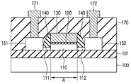
- FIG. 1 is a plan view showing an element structure of a semiconductor device according to a first embodiment.
- FIG. 2 is a cross-sectional view in the direction of arrows II in FIG. 1.
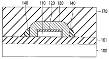
- FIG. 2 is a cross-sectional view in the direction of arrows II-II in FIG.
- Sectional drawing which shows the element structure of the modification of 1st Embodiment.
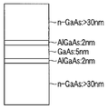
- Sectional drawing which shows an example of RTD using the heterostructure of GaAs and AlGaAs.
- FIG. 3 is a diagram showing a ground level of each region in the semiconductor device of the first embodiment.
- FIG. which shows the relationship between the incident electron energy and the transmission probability (tau) in the element structure of FIG.
- the figure which shows the electric current and voltage characteristic of the element structure shown in FIG. The figure which shows the energy band structure in each voltage application state of the element structure shown in FIG.
- Sectional drawing which shows the manufacturing process of the semiconductor device concerning 1st Embodiment.
- Sectional drawing which shows the manufacturing process of the semiconductor device concerning 1st Embodiment.
- Sectional drawing which shows the manufacturing process of the semiconductor device concerning 1st Embodiment.
- Sectional drawing which shows the manufacturing process of the semiconductor device concerning 1st Embodiment.
- Sectional drawing which shows the manufacturing process of the semiconductor device concerning 1st Embodiment Sectional drawing which shows the manufacturing process of the semiconductor device concerning 1st Embodiment.
- the circuit block diagram which shows the semiconductor device concerning 2nd Embodiment.
- Sectional drawing which shows the element structure of the semiconductor device concerning 3rd Embodiment.
- FIG. 22 is a cross-sectional view in the direction of arrows III-III in FIG. 19.
- FIG. 20 is a cross-sectional view in the direction of arrow IV-IV in FIG.
- FIG. 1 to 3 are diagrams for explaining the element structure of the semiconductor device according to the first embodiment of the present invention.
- FIG. 1 is a plan view
- FIG. 2 is a sectional view taken in the direction of arrows II in FIG. 3 is a cross-sectional view taken along the line II-II in FIG.
- the semiconductor device is a negative differential resistance element using the negative differential resistance characteristics of a semiconductor, and is manufactured on an SOI wafer. That is, a buried insulating film (BOX) 101 is provided on a support substrate (semiconductor substrate) 100, and a first channel region 110 and second channel regions 111 and 112 are provided on the buried insulating film 101. ing.
- the channel regions 110, 111, and 112 are both formed of single crystal silicon (Si), and the channel regions 111 and 112 are provided in contact with the channel region 110 so as to sandwich the channel region 110 from the lateral direction (channel length direction). ing.
- the thickness of Si in the direction perpendicular to the wafer surface in the channel region 110 is thicker than the thickness of Si in the direction perpendicular to the wafer surface in the channel regions 111 and 112. This is because, as will be described later, a negative differential resistance characteristic is exhibited by the difference in Si thickness between the channel region 110 and the channel regions 111 and 112 in the direction perpendicular to the wafer surface.
- the support substrate 100 is made of single crystal Si, and preferably contains the same type of impurities as the channel regions 110, 111, and 112 at the same concentration.
- the channel regions 110, 111, and 112 and the support substrate 100 are generated between the channel regions 110, 111, and 112 and the support substrate 100 in the direction perpendicular to the wafer surface. Eliminate the built-in electric field.
- the wave function of electrons in the channel region 110, 111, 112 in the vertical direction of the wafer surface to spread throughout the channel region 110, 111, 112, a net current path in the vertical direction of the wafer surface can be obtained. It becomes possible to increase. If the net current path in the direction perpendicular to the wafer surface increases, the amount of current per unit area in the wafer surface will increase, and the size of the semiconductor device necessary to obtain the desired amount of current can be reduced. High integration of the semiconductor device can be realized.
- the thickness of the buried insulating film 101 of the SOI wafer is sufficiently thick as 10 nm or more, and the leakage current between the channel regions 110, 111, and 112 and the support substrate 100 is completely suppressed.
- the thickness of the buried insulating film 101 is 10 nm or more, the leakage current due to direct tunneling is completely suppressed, and therefore, a resonant tunneling phenomenon occurs between the channel regions 110, 111, and 112 and the support substrate 100. Can be completely suppressed. Thereby, the design for obtaining a desired negative differential resistance characteristic becomes easy.
- the buried insulating film 101 is preferably made of a material having excellent flatness at the interface with the channel regions 110, 111, and 112, such as silicon dioxide (SiO 2 ). This is because if the flatness of the interface between the buried insulating film 101 and the channel regions 110, 111, and 112 is excellent, scattering of electrons traveling through the channel regions 110, 111, and 112 is suppressed due to the unevenness of the interface, and thus negative This is because the differential resistance characteristic is easily developed.
- a gate insulating film 120 is formed on the channel region 110, and sidewall insulating films 140 are formed on the channel regions 111 and 112, respectively.
- the material of the insulating films 120 and 140 is preferably silicon dioxide (SiO 2) or the like having excellent flatness at the interface with the channel regions 110, 111 and 112. As in the case of the buried insulating film 101, if the flatness of the interface with the channel regions 110, 111, and 112 is excellent, scattering of electrons traveling through the channel regions 110, 111, and 112 due to the unevenness of the interface is caused. This is because the negative differential resistance characteristic is easily exhibited because of being suppressed.
- a gate electrode 130 made of metal or polysilicon is formed immediately above the gate insulating film 120.
- the sidewall insulating film 140 is formed so as to cover the side surface of the gate electrode 130.
- the reason why the gate electrode 130 is necessary and that the sidewall insulating film 140 is formed so as to cover the side surface of the gate electrode 130 is to facilitate the manufacturing process of the semiconductor device, as will be described later. .
- the gate insulating film 120 and the gate electrode 130 do not actually have their original functions, but are formed at the same time as the gate portion of the peripheral transistor as will be described later.
- they are referred to as a gate insulating film and a gate electrode.
- the gate electrode 130 is a gate electrode material film
- the gate insulating film 120 is a gate insulating material film.
- the gate electrode 130 is not always necessary, and even if the film 130 does not exist, the operation of the semiconductor device according to the present embodiment is possible.
- the structure in which the gate electrode 130 does not exist is the design example of the semiconductor device according to the first embodiment. Included in the range.
- the sidewall insulating film 140 is formed so as to cover the side surface of the gate electrode 130 for the purpose of facilitating the manufacturing process.
- the sidewall insulating film 140 is formed immediately above the channel regions 111 and 112. Existence is important for the operation of the semiconductor device according to the present embodiment. Therefore, for example, when the sidewall insulating film 140 is once formed and then peeled, and then the insulating film 160 is formed, as a result, as shown in FIG. It falls within the scope of the design example of the semiconductor device according to the first embodiment.
- the electrode regions 151 and 152 are formed on the buried insulating film 101 so as to be directly bonded to the side of the channel regions 111 and 112. That is, the electrode regions 151 and 152 are formed so as to sandwich the channel regions 110, 111, and 112 from the channel length direction.
- the electrode regions 151 and 152 are made of n-type Si containing impurities such as As (arsenic) and P (phosphorus), for example. Further, the thickness of Si in the direction perpendicular to the wafer surface of the electrode regions 151 and 152 is larger than the thickness of Si in the direction perpendicular to the wafer surface of the channel region 110.
- an interlayer insulating film 170 is formed so as to cover the surface portion of the substrate on which the gate electrode 130, the sidewall insulating film 140, and the electrode regions 151 and 152 are formed.
- the correlation insulating film 170 is formed with plug electrodes 171 and 172 for connection to the electrode regions 151 and 152, respectively. That is, the element of this embodiment is a two-terminal element.
- the channel regions 111 and 112 In order to develop negative differential resistance characteristics in the channel regions 110, 111, and 112, it is necessary to use the channel regions 111 and 112 as an energy barrier against electrons.
- the electrode regions 151 and 152 By making the thickness of Si in the vertical direction of the wafer surface of the electrode regions 151 and 152 thicker than Si in the vertical direction of the wafer surface of the channel region 110, the electrode regions 151 and 152 are compared with the channel regions 111 and 112. As a result, electrons can exist at a low energy position. As a result, the channel regions 111 and 112 can be used as energy barriers against electrons.
- the electrode regions 151 and 152 are used as a source of free electrons.
- the electrode regions 151 and 152 are formed from n-type Si containing impurities such as As and P, for example, it becomes possible to have many free electrons in the electrode regions 151 and 152.
- FIG. 5 shows a structure of an element using gallium arsenide (GaAs) and aluminum gallium arsenide (AlGaAs), which is an example of an RTD using a heterostructure.
- GaAs gallium arsenide
- AlGaAs aluminum gallium arsenide
- FIG. 5 shows a structure of an element using gallium arsenide (GaAs) and aluminum gallium arsenide (AlGaAs), which is an example of an RTD using a heterostructure.
- GaAs gallium arsenide
- AlGaAs aluminum gallium arsenide
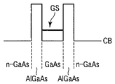
- FIG. 6 shows an energy band structure of the element structure shown in FIG.
- the band gap of AlGaAs is larger than the band gap of GaAs, and when AlGaAs and GaAs are joined, an energy barrier is created against electrons at the interface between the two. Further, when the film thickness of GaAs sandwiched between AlGaAs is about 10 nm or less, the quantization of energy levels in GaAs sandwiched between AlGaAs becomes significant.
- the ground level which is the lowest energy level, exists at a position higher in energy than the lower end of the conduction band.
- the probability that an electron exists in an energy position where there is no energy level between the quantized energy levels is very low.
- a large number of free electrons are present in n-type GaAs containing impurities at a high concentration adjacent to AlGaAs, and acts as a source of free electrons.
- the device When a voltage is applied to the device between the upper and lower n-GaAs layers, the device exhibits a special behavior due to the energy band structure depending on the magnitude of the applied voltage. That is, when the voltage becomes higher than a predetermined value, current starts to flow, the current increases as the voltage increases, and when the applied voltage is further increased, the current hardly flows. That is, it is possible to develop a negative differential resistance characteristic that current decreases as voltage increases.
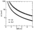
- FIG. 7 shows a calculated value of energy from the lower end of the conduction band of the ground level GS and the first excitation level EL1 among the energy levels quantized by the quantum confinement effect as a function of the thickness of Si.
- Si is thinned in the ⁇ 001> direction and sandwiched between layers that serve as an energy barrier against electrons, such as SiO2.
- the ground level GS is 16 meV when the lower end of the Si conduction band is the origin of energy
- the first excitation level EL1 is 66 meV
- the thickness of Si is 2 nm.
- the ground level GS is 103 meV.
- the channel region 110 when the channel region 110 is 5 nm and the channel regions 111 and 112 are 2 nm, the channel regions 100, 111, 112, and the electrode regions 151, The ground level GS of 152 is shown.
- the electrode region 151 is an electron supply source
- the channel regions 111 and 112 are energy barriers for electrons
- the channel region 110 sandwiched between the energy barriers is a region where energy levels are quantized.
- the energy splitting amount between the ground level GS and the first excitation level EL1 in the channel region 110 is 50 meV, which is sufficiently larger than the thermal energy (25 meV) at room temperature. It is thought that the influence of quantization is retained.
- the Si thickness of the channel regions 110, 111, and 112 is thinner than the Si thickness of the channel region 110. Further, the Si thickness of the channel region 110 is such that the amount of energy splitting between the ground level GS and the first excitation level EL1 in the channel region 110 is larger than the thermal energy (25 meV) at room temperature. It is necessary to. Arbitrary Si thicknesses of the channel regions 110, 111, and 112 satisfying such restrictions are included in the range of the semiconductor device design example according to the present embodiment.
- the effective mass the more significant the energy level quantization.
- the effective mass of electrons is smaller than the effective mass of holes. For this reason, when the carriers traveling in the channel regions 110, 111, and 112 are electrons, the quantization of the energy level becomes more remarkable, and the negative differential resistance characteristics at room temperature can be easily expressed. Therefore, it is desirable that the carrier of the current flowing through the channel regions 110, 111, and 112 when the voltage is applied is carriers.
- an energy barrier for two electrons and an energy level existing between them are provided in the wafer in-plane direction.
- a quantized region is provided. That is, the semiconductor device according to the present embodiment is adjacent to two energy barriers necessary for expressing the negative differential resistance characteristics, a region where the energy level existing between them is quantized, and the energy barrier. It has an electron source.
- the length of the channel region 110 (the length indicated by the arrow A in FIG. 2) is desirably 10 nm or less. In order to exhibit the negative differential resistance characteristic, it is required to suppress the scattering of electrons in the channel region 110 as much as possible.
- the average electron scattering frequency is 1 ⁇ 10 ⁇ 11 [1 / s] and the electron velocity is 1 ⁇ 10 7 [cm / s].
- the distance that the vehicle can travel without being stopped is about 10 nm. For this reason, the length of the channel region 110 is desirably 10 nm or less in the direction in which the current flows.
- the length of the channel region 110 in the direction in which the current flows is determined when the gate electrode 130 is processed by a manufacturing process described later.
- the gate electrode 130 can be processed using the same manufacturing process as that of the conventional MOSFET gate, and the length of the channel region 110 in the direction of current flow is processed as designed with good controllability. It is possible.
- the current is given by an integral obtained by weighting the transmission probability ⁇ with a function of electron energy, and the characteristic of the transmission probability ⁇ greatly affects the current / voltage characteristics.
- Various methods have been proposed for calculating the transmission probability ⁇ (references 1 and 2).
- FIG. 9 shows the relationship between the transmission probability ⁇ and the energy of electrons input from the electrode region 151 in the semiconductor device according to this embodiment, calculated by the method proposed in Reference Document 2, when the applied voltage is small.
- the transmission probability ⁇ increases at first, but decreases at 16 meV. This is because, in the semiconductor device according to the present embodiment, the ground level GS in the channel region 110 is energetically lower than the Fermi energy of the electrode region 151 that is an electron supply source, so that the electron transmission probability ⁇ is It corresponds to the decrease. That is, the negative differential resistance characteristic is manifested in the semiconductor device of this embodiment.
- the energy difference between the quantized ground level GS and the first excitation level EL1 in the channel region 110 is 25 meV or more which is the thermal energy at room temperature. is required.
- the Si thickness of the channel region 110 is 7 nm or less.
- the energy difference between the ground levels of the channel region 110 and the channel regions 111 and 112 needs to be at least 25 meV.
- the Si thicknesses of the channel region 110 and the channel regions 111 and 112 have the following relationship.
- FIG. 10 shows the current / voltage characteristics when a voltage is applied to the element shown in FIG. 8, and FIGS. 11A to 11C show the energy band structure in each voltage application state.
- the ground level in the channel region 110 is representative energy of electrons in the channel region 111 which is an electron supply source. The current starts to flow because it is close in energy to the Fermi energy.
- an energy barrier for two electrons, a region where the energy level existing between them is quantized, and a source of electrons adjacent to the energy barrier is required.
- FIG. 12A to 15A show this embodiment
- FIG. 12B shows a conventional MOSFET.
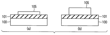
- an SOI substrate is prepared in which a Si layer (SOI layer) 105 is formed on a Si substrate 100 with a buried insulating film 101 interposed therebetween. Then, as shown in FIG. 12A, the SOI layer 105 in the region where the semiconductor device according to this embodiment is manufactured is thinned. At this time, it is possible to reduce the thickness of the SOI layer 105 in the region where the MOSFET is manufactured. However, in this embodiment, a case where the thickness is not reduced as shown in FIG.
- the peripheral region of the SOI layer 105 used in the semiconductor device of this embodiment is removed.
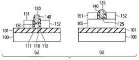
- the gate insulating film 120 and the gate electrode are selectively etched by RIE (Reactive) Ion Etching). 130 is formed.
- the thickness of Si in the channel region 110 located under the gate electrode 130 is set to be larger than the thickness of Si in the SOI layer in which the gate electrode 130 does not exist above.
- an oxide film (not shown) is formed on the surface of the SOI layer where the gate electrode 130 does not exist on the upper portion, and this oxide film is peeled off by wet etching with a chemical solution. The reason why the oxide film is peeled after the oxide film is formed is to planarize the surface of the SOI layer where the gate electrode 130 does not exist on the top.
- a mask or the like is used for the MOSFET in the peripheral region mixedly mounted on the same wafer. Protected by. After the oxide film is peeled off, the semiconductor device of this embodiment is protected with a mask or the like, the gate processing of the MOSFET in the peripheral region, and desired impurity implantation are performed.
- the gate insulating film 125 is formed by processing the insulating film
- the gate electrode 135 is formed by processing the conductive film.
- a source / drain region (not shown) is formed by implanting impurities. Thereafter, the mask or the like protecting the semiconductor device of this embodiment is removed.
- a sidewall insulating film 140 is formed on the side surfaces of the gate electrodes 130 and 135. This process is performed simultaneously in the semiconductor device of this embodiment and the MOSFET in the peripheral region.
- Si is stacked on the SOI region where the side wall insulating film 140 does not exist on the upper portion to form electrode regions 151 and 152. Further, by introducing impurities such as arsenic (As) and phosphorus (P) into the electrode regions 151 and 152 and performing impurity activation annealing, the electrode regions 151 and 152 are made to have high conductivity n-type Si. .
- the electrode regions 151 and 152 of the semiconductor device of this embodiment are formed, the same process is performed for the MOSFET in the peripheral region, but the performance of the MOSFET is not deteriorated. Don't be.
- the gate insulating film 120 and the gate electrode 130 are made of the same material as the gate insulating film 125 and the gate electrode 135 of the MOSFET mixedly mounted on the same wafer, respectively, thereby simplifying the manufacturing process. That is, the manufacturing process of the semiconductor device according to the present embodiment has good consistency with the manufacturing process of the conventional MOSFET, and can be easily mounted on the same wafer as the conventional MOSFET.
- the semiconductor device includes the two electrode regions 151 and 152 manufactured on the SOI wafer, and the SOI layer between the electrode regions 151 and 152 is changed from one electrode region 151 to the other electrode.
- the region 152 is divided into three regions as follows according to the thickness of Si in the direction perpendicular to the wafer surface of the SOI layer toward the region 152.
- the thickness of Si in the direction perpendicular to the wafer surface of the first SOI layer region (second channel region) 111 and the third SOI layer region (second channel region) 112 is determined as the second SOI layer.
- the region (first channel region) 110 is made thinner than the thickness of Si in the direction perpendicular to the wafer surface, the insulating film 120 is formed on the SOI layer region 110, and the insulating film 140 is formed on the SOI layer regions 111 and 112. To do.
- the two electrode regions 151 and 152 are respectively replaced with the source region and the drain region of the conventional MOSFET, the insulating film on the SOI layer region 110 is used as the gate insulating film, and the insulating film on the SOI layer regions 111 and 112 is used as the insulating film. If the side wall formed on the side of the gate is substituted, it is possible to manufacture with good consistency with the Si-based manufacturing process for manufacturing the conventional MOSFET, and it becomes easy to mount the conventional MOSFET on the same wafer.
- an RT-SRAM having a memory operation function is configured by combining the semiconductor device (negative differential resistance element) of the first embodiment with a transistor and a capacitor.
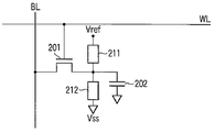
- an RT-SRAM functioning as a memory cell is formed at the intersection of the bit line BL and the word line WL.
- the gate electrode of the MOS transistor 201 is connected to the word line WL, one of the source / drain regions is connected to the bit line, and the other of the source / drain regions is connected to the ground terminal via the capacitor 202.
- negative differential resistance elements 211 and 212 of the first embodiment are provided.
- one electrode region of the first negative differential resistance element 211 is connected to a storage node (SN) that is a connection point between the MOS transistor 201 and the capacitor 202, and the other electrode region of the negative differential resistance element 211 is desired. Is connected to an external electronic circuit so as to maintain the voltage Vref.
- One electrode region of the second negative differential resistance element 212 is connected to SN, and the other electrode region of the negative differential resistance element 212 is connected to an external electronic circuit so as to maintain a desired voltage Vss. .
- Vref is a potential higher than Vss.
- the state where the SN potential is Vref is referred to as “1” state
- the state where the SN potential is Vss is referred to as “0” state.
- a case where “1” is written when the initial state is “0” and “1” is read after a predetermined time will be described as an example.
- reading of the information held in the SN increases the potential of the word line WL, electrically connects the source / drain regions of the MOSFET 201, and charges accumulated in the SN are supplied to the amplifier through the bit line BL. Do this by typing.
- FIG. 17 is a cross-sectional view showing an element structure of a semiconductor device according to the third embodiment of the present invention, and shows a cross section along the channel length direction as in FIG.
- reference numerals 300, 310, 311, 312, 320, 330, 340, 351, 352, 370, 371, and 372 in the figure denote 100, 110, 111, 112, 120, 130, 140, and 151, respectively. 152, 170, 171 and 172, respectively.
- the semiconductor device of the present embodiment is the same as that of the first embodiment except that the shape of the buried insulating film 301 is different, so that the description of the same parts as those of the first embodiment is omitted.
- the buried insulating film 301 exists only under the first channel region 310, the second channel regions 311, 312 and the electrode regions 351, 352.
- the bulk silicon wafer 300 can be used as will be described later. Therefore, it can be mixed with peripheral circuits manufactured on the bulk silicon wafer 300.
- the manufacturing process becomes complicated as will be described later, but the material cost can be reduced.
- an Si region in which a semiconductor device is manufactured is formed on the surface portion of the Si substrate 300 using STI (Shallow Trench Isolation) or LOCOS (Local Oxidation of Silicon).
- An element isolation insulating film 360 for electrically isolating from the Si region is formed.
- the SiGe layer 303 is epitaxially grown, and the Si layer 305 is epitaxially grown thereon.
- the gate insulating film 320 and the gate electrode 330 are formed by selectively etching them. Further, when the gate insulating film 320 and the gate electrode 330 are processed, the Si thickness of the first channel region 310 located under the gate electrode film 330 is the second channel in which the gate electrode film 330 does not exist above. It is made thicker than the thickness of the regions 311 and 312.
- a buried insulating film 301 made of an oxide film is formed in the cavity formed by removing the SiGe layer 303. Even if the SiGe layer 303 is removed, the Si layer 305 (channel regions 310, 311 and 312) is supported by the gate insulating film 320 and the gate electrode film 330, and therefore does not fall down. Further, the removal of the SiGe layer 303 and the formation of the buried insulating film 301 are performed by opening a hole in the direction perpendicular to the wafer surface in a part of the STI or LOCOS that electrically isolates the semiconductor device of this embodiment from the periphery. Do.
- the oxide film is removed by wet etching with a chemical solution.
- the reason why the oxide film is peeled off after the oxide film is formed is to flatten the surface of the Si layer where the gate electrode material film 330 does not exist on the top.
- the structure shown in FIG. 17 is obtained by forming the sidewall insulating film 340 and further forming the electrode regions 351 and 352 and the like.
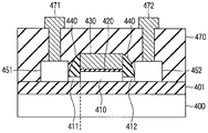
- FIG. 19 to 21 are for explaining the element structure of the semiconductor device according to the fourth embodiment of the present invention.
- FIG. 19 is a plan view
- FIG. 20 is a cross-sectional view taken along the line III-III in FIG. 21 is a cross-sectional view in the direction of arrows IV-IV in FIG.
- reference numerals 400, 410, 411, 412, 420, 430, 440, 451, 452, 470, 471, 472 denote 100, 110, 111, 112, 120, 130, 140, 151, 152, 170, 171 and 172, respectively.
- the basic structure is the same as that of the first embodiment, but in this embodiment, a plurality of current paths including SOI layers existing between the electrode region 451 and the electrode region 452 are provided.
- FIG. 19 shows a case where there are three current paths made of SOI layers as an example.
- the first channel region 410 has a square cross section, but the cross sectional shape is arbitrary and does not necessarily have to be a square.
- the semiconductor device of this embodiment is manufactured on an SOI wafer.
- the first channel region 410 and the second channel regions 411 and 412 are formed of the gate insulating film 420 in all directions perpendicular to the direction of current flowing between the electrode regions 451 and 452. And a buried insulating film 401.
- the gate insulating film 420 is surrounded by the gate electrode film 430.
- the length of the channel region 410 in the direction in the wafer plane and perpendicular to the direction of the current flowing between the electrode region 451 and the electrode region 452 is the length of the channel region 410 in the direction perpendicular to the wafer surface. It is desirable to be about 1.7 times.
- the energy level in the channel region 410 is significantly quantized.
- the semiconductor device of this embodiment since the channel region 410 is surrounded by the gate insulating film 420 and the buried insulating film 401, electrons in the channel region 410 flow between the electrode region 451 and the electrode region 452.
- the quantum confinement effect acts in all directions perpendicular to the current direction. Therefore, the quantization of the energy level in the channel region 410 occurs more significantly than in the first embodiment.
- the semiconductor device of this embodiment is manufactured on a (001) -plane SOI wafer in accordance with a conventional manufacturing process. This is desirable because it can.
- the direction in the wafer plane and the direction perpendicular to the direction of the current flowing between the electrode region 451 and the electrode region 452 is: ⁇ 110> direction.
- ⁇ 110> direction of Si there are two types of effective masses of electrons of 0.315 m 0 and 0.19 m 0 .
- m 0 is the mass of electrons in vacuum.
- ⁇ 110> direction of the larger effective mass 0.315M 0 is a wafer plane straight direction ⁇ 001> directions of the two kinds of 0.91 m 0 and 0.19 m 0 is the effective mass, the larger the effective of The mass is about 1/3 of 0.91 m 0 .
- the strength of the quantum confinement effect is inversely proportional to the effective mass and inversely proportional to the square of the thickness in the confinement direction. Therefore, when the film thickness of Si in the ⁇ 110> direction is about 1.7 times the film thickness of Si in the ⁇ 001> direction, two types of effective masses are present in the ⁇ 110> direction and the ⁇ 001> direction.
- the quantum confinement effect of the same strength works for electrons with a large effective mass.
- the quantum confinement effect in the ⁇ 110> direction is thinner than about 1.7 times the film thickness of Si in the ⁇ 001> direction, the quantum confinement effect in the ⁇ 110> direction is greater than the quantum confinement effect in the ⁇ 001> direction. Becomes a major factor in determining the overall energy level.
- the two types of effective masses in the ⁇ 110> direction are close in value to those in the ⁇ 001> direction. Therefore, if attention is paid to one effective mass, the conduction of quantized energy levels The amount of energy increase from the bottom of the belt is large. However, the amount of energy splitting between quantized energy levels due to different effective masses is small compared to the ⁇ 001> direction. Therefore, when the quantum confinement effect in the ⁇ 110> direction is a main factor for determining the overall energy level, a small amount of energy split between the quantized energy levels in the channel region 410 becomes negative differential resistance. This adversely affects the development of characteristics.
- the length of the channel region 410 in the direction in the wafer plane and perpendicular to the direction of the current flowing between the electrode region 451 and the electrode region 452 is one of the length of the channel region 410 in the direction perpendicular to the wafer surface. It is desirable to be about 7 times.
- the semiconductor device according to this embodiment can be manufactured by the same manufacturing process as that of the first embodiment, the description of the manufacturing process of the semiconductor device of this embodiment is omitted.
- a bulk Si substrate is used in place of the SOI substrate in the configuration of the semiconductor device of the fourth embodiment described above.
- it can be produced by the same method as in the third embodiment except that a plurality of Si layers are formed.
- the shape of the buried insulating film is different, it is the same as the semiconductor device of the fourth embodiment, and the sectional view corresponding to FIG. 19 of the fourth embodiment is the same as FIG.
- Electrons are responsible for the current that flows in the channel region.
- the length of the first channel region in the channel length direction is 10 nm or less.
- the first and second channel regions are surrounded by an insulating film and are perpendicular to the direction of the current flowing between the two electrode regions. With respect to this direction, at least half of the outer periphery of the insulating film surrounding the first and second channel regions is surrounded by the gate electrode material film.
- the insulating film under the Si region where the first and second channel regions are formed exists only under the channel region and the electrode region.
- the characteristic steps as a manufacturing method are as follows.
- a Si layer to be a first channel region, a second channel region sandwiching the channel region from one direction, and an electrode region sandwiching the first and second channel regions from the one direction (2)
- a step of forming a gate electrode through a gate insulating film on the portion to be the first channel region on the Si layer (3)
- a part of the Si layer using the gate electrode as a mask The step of thinning the Si layer of the portion to be the second channel region and the portion to be the electrode region by etching (4)
- the side wall of the gate electrode and the portion to be the second channel region of the Si layer Step of forming sidewall insulating film on top (5)
- a new Si layer is grown on the Si layer not covered with the gate electrode or the sidewall insulating film, thereby reducing the thickness of the Si layer to be the electrode region.
- Si of the portion to be the first channel region Step thicker than the thickness (variation) The present invention is not limited to the above-described embodiments.
- the description of the semiconductor device, the manufacturing process of the semiconductor device, etc., which is not directly necessary for the description of the present invention is omitted, but the required semiconductor device, the manufacturing process of the semiconductor device, etc.
- the elements related to can be appropriately selected and used.
- 100, 300, 400 ... support substrate (semiconductor substrate) 101, 301, 401 ... buried insulating film 105 ... SOI layer 110, 310, 410 ... first channel region 111, 112, 311, 312, 411, 412 ... second channel region 120, 125, 320, 420 ... gate Insulating film 130, 135, 330, 430 ... Gate electrode 140, 340, 440 ... Side wall insulating film 151, 152, 351, 352, 451, 452 ... Electrode region 160 ... Insulating film 170, 370, 470 ... Interlayer insulating film 171, 172, 371, 372, 471, 472 ... plug electrode 201 ... MOS transistor 202 ... capacitor 211 ... first negative differential resistance element 212 ... second negative differential resistance element 303 ... SiGe layer 305 ... Si layer 360 ... element Isolation insulation film
Landscapes
- Engineering & Computer Science (AREA)
- Computer Hardware Design (AREA)
- Metal-Oxide And Bipolar Metal-Oxide Semiconductor Integrated Circuits (AREA)
Abstract
負性微分抵抗特性を有する半導体装置であって、絶縁膜上に設けられ、Siで形成された第1のチャネル領域と、第1のチャネル領域を挟んで前記絶縁膜上にそれぞれ設けられ、第1のチャネル領域よりも膜厚の薄いSiで形成された2つの第2のチャネル領域と、第1及び第2のチャネル領域を挟んで絶縁膜上に設けられ、且つ第2のチャネル領域に対して第1のチャネル領域と反対側にそれぞれ設けられ、第1のチャネル領域よりも膜厚の厚いSiで形成された2つの電極領域とを備え、電極領域間への電圧の印加により電極領域間に負性微分抵抗特性を発現させる。
Description
本発明は、半導体の負性微分抵抗特性を利用した半導体装置に関する。
近年、リフレッシュ動作を不要とするレゾナントトンネリングSRAM(Resonant Tunneling SRAM:以下RT-SRAMと略記する)が提案されている。このRT-SRAMは、情報の書き込みと読み出しにDRAMと同様の機構を用い、情報となる電位を保持するノードに負性微分抵抗特性を有するレゾナントトンネリングダイオード(RTD:Resonant Tunneling Diode)を2つ接続することにより、リフレッシュ動作を不要にしている(特許文献1参照)。
RT-SRAMでは、従来の半導体プロセスで作製されるDRAMと、特性の優れた負性微分抵抗特性を有するRTD等の負性微分抵抗素子を如何に混載するかが課題となっている。従来、負性微分抵抗素子として、
(a) III-V族半導体を主とする化合物半導体のヘテロ構造を利用したRTD(特許文献1参照)
(b) IV族半導体のヘテロ構造を利用したRTD
(c) Siベースのサーフェスジャンクショントンネリング(SJT:Surface Junction Tunneling)を利用した素子(特許文献2参照)
等が提案されている。
(a) III-V族半導体を主とする化合物半導体のヘテロ構造を利用したRTD(特許文献1参照)
(b) IV族半導体のヘテロ構造を利用したRTD
(c) Siベースのサーフェスジャンクショントンネリング(SJT:Surface Junction Tunneling)を利用した素子(特許文献2参照)
等が提案されている。
しかし、(a) の素子は、DRAMと混載する際の製造プロセスとの整合性が良くない。(b) の代表例としてSiとSiGeのヘテロ構造があるが、RTDの電極領域を他素子の電極領域や電子回路に接続するという従来のSiベースの製造プロセスにはないプロセスが必要であり、Siベースの製造プロセスとの整合性が良くない。(c) の素子は、3端子素子であり、2端子素子と比べて1つの接続端子を余計に必要とするため、接続端子分だけ素子の大きさが増大する。素子の大きさが増大すると、単位面積当たりに製造できる素子数が減少するため、単位面積当たりのメモリ容量が減ってしまう。
本発明の目的は、2端子素子で負性微分抵抗特性を発現することができ、且つ従来のSiベースの半導体プロセスとの整合性が良い半導体装置を提供することにある。
本発明の一態様に係わる半導体装置は、絶縁膜上に設けられ、Siで形成された第1のチャネル領域と、前記第1のチャネル領域を挟んで前記絶縁膜上にそれぞれ設けられ、前記第1のチャネル領域よりも膜厚の薄いSiで形成された2つの第2のチャネル領域と、前記第1及び第2のチャネル領域を挟んで前記絶縁膜上に設けられ、且つ前記第2のチャネル領域に対して前記第1のチャネル領域と反対側にそれぞれ設けられ、前記第1のチャネル領域よりも膜厚の厚いSiで形成された2つの電極領域と、を具備し、前記電極領域間への電圧の印加により、前記電極領域間に負性微分抵抗特性を発現させることを特徴とする。
また、本発明の別の一態様は、スイッチング用トランジスタ及びキャパシタが接続されるストレージノードと第1の電位端との間に負性微分抵抗特性を有する第1の負性微分抵抗素子を接続し、且つ前記ストレージノードと第2の電位端との間に負性微分抵抗特性を有する第2の負性微分抵抗素子を接続した半導体装置であって、前記各負性微分抵抗素子はそれぞれ、半導体基板上に形成された絶縁膜上に設けられ、Siで形成された第1のチャネル領域と、前記第1のチャネル領域を挟んで前記絶縁膜上にそれぞれ設けられ、前記第1のチャネル領域よりも膜厚の薄いSiで形成された2つの第2のチャネル領域と、前記第1及び第2のチャネル領域を挟んで前記絶縁膜上に設けられ、且つ前記第2のチャネル領域に対して前記第1のチャネル領域と反対側にそれぞれ設けられ、前記第1のチャネル領域よりも膜厚の厚いSiで形成された2つの電極領域と、を具備したことを特徴とする。
本発明によれば、2端子素子で負性微分抵抗特性を発現することができ、且つ製造プロセスが、従来のSiベースの製造プロセスと整合性が良い半導体装置を実現することができる。
以下、本発明の詳細を図示の実施形態によって説明する。なお、図面は、概念を説明するためのものであり、図面中の素子寸法の大小関係は、実物の素子寸法の大小関係とは、必ずしも一致するものではない。
(第1の実施形態)
図1乃至図3は、本発明の第1の実施形態に係わる半導体装置の素子構造を説明するためのもので、図1は平面図、図2は図1の矢視I-I方向断面図、図3は図1の矢視II-II方向断面図である。
図1乃至図3は、本発明の第1の実施形態に係わる半導体装置の素子構造を説明するためのもので、図1は平面図、図2は図1の矢視I-I方向断面図、図3は図1の矢視II-II方向断面図である。
本実施形態に係わる半導体装置は、半導体の負性微分抵抗特性を利用した負性微分抵抗素子であり、SOIウエハ上に製造される。即ち、支持基板(半導体基板)100上に埋め込み絶縁膜(BOX:Buried Oxide)101が設けられ、この埋め込み絶縁膜101上に第1のチャネル領域110と第2のチャネル領域111,112が設けられている。チャネル領域110,111,112は、共に単結晶シリコン(Si)で形成され、チャネル領域111,112はチャネル領域110を横方向(チャネル長方向)から挟むように、チャネル領域110に接して設けられている。
チャネル領域110のウエハ面垂直方向のSiの厚さは、チャネル領域111,112のウエハ面垂直方向のSiの厚さよりも厚くなっている。これは、後述するように、チャネル領域110とチャネル領域111,112のウエハ面垂直方向のSiの厚さの違いにより、負性微分抵抗特性を発現させるためである。
支持基板100は、単結晶Siで形成されており、チャネル領域110,111,112と同種の不純物を同濃度で含有していることが望ましい。チャネル領域110,111,112と支持基板100が、同種の不純物を同濃度で含有するようにすることで、ウエハ面垂直方向の、チャネル領域110,111,112と支持基板100との間に発生する内蔵電界を無くする。そして、チャネル領域110,111,112内の、ウエハ面垂直方向の電子の波動関数が、チャネル領域110,111,112内全体に広がるようにすることで、ウエハ面垂直方向の正味の電流路を増やすことが可能となる。ウエハ面垂直方向の正味の電流路が増えると、ウエハ面内での単位面積当たりの電流量が増大することになり、所望の電流量を得るために必要な半導体装置の大きさを小さくでき、半導体装置の高集積化が可能となる。
SOIウエハの埋め込み絶縁膜101の厚さは、10nm以上と十分に厚く、チャネル領域110,111,112内と支持基板100との間のリーク電流が完全に抑制されることが望ましい。特に、埋め込み絶縁膜101の厚さが10nm以上であると、直接トンネルによるリーク電流が完全に抑制されるため、チャネル領域110,111,112内と支持基板100との間に共鳴トンネル現象が発生するのを完全に抑制することができる。これにより、所望の負性微分抵抗特性を得るための設計が容易となる。
また、埋め込み絶縁膜101は、二酸化シリコン(SiO2)等、チャネル領域110,111,112との界面の平坦性が優れている材料であることが望ましい。これは、埋め込み絶縁膜101とチャネル領域110,111,112との界面の平坦性が優れていると、界面の凹凸にチャネル領域110,111,112を走行する電子の散乱が抑制され、負性微分抵抗特性が発現しやすくなるからである。
チャネル領域110上にはゲート絶縁膜120が形成され、チャネル領域111,112上にはそれぞれ、側壁絶縁膜140が形成されている。絶縁膜120,140の材料は、チャネル領域110,111,112との界面の平坦性に優れる二酸化シリコン(SiO2)等であることが望ましい。これは、埋め込み絶縁膜101の場合と同様に、チャネル領域110,111,112との界面の平坦性が優れていると、界面の凹凸によるチャネル領域110,111,112を走行する電子の散乱が抑制されるため、負性微分抵抗特性が発現しやすくなるからである。
ゲート絶縁膜120の直上には、金属若しくはポリシリコンから構成されるゲート電極130が形成されている。また、側壁絶縁膜140は、ゲート電極130の側面を覆うように形成されている。ゲート電極130が必要なこと、及び側壁絶縁膜140がゲート電極130の側面を覆うように形成されていることが必要である理由は、後述するように、半導体装置の製造プロセスの容易化である。
なお、本実施形態装置がMOSトランジスタではないために、ゲート絶縁膜120及びゲート電極130は実際には本来の機能を有しないが、後述するようにこれらを周辺トランジスタのゲート部分と同時に形成するために、ここではゲート絶縁膜及びゲート電極と称している。より正確に言うならば、ゲート電極130はゲート電極材料膜であり、ゲート絶縁膜120はゲート絶縁材料膜である。
また、ゲート電極130は必ずしも必要ではなく、この膜130が存在しなくても、本実施形態に係わる半導体装置の動作は可能である。例えば、ゲート電極130が一度形成された後に、剥離されることで、図4に示すように、結果として、ゲート電極130が存在しない構造は、第1の実施形態に係わる半導体装置の設計例の範囲に含まれる。
また、側壁絶縁膜140が、ゲート電極130の側面を覆うように形成されていることは、製造プロセスの容易化を目的としたものであり、チャネル領域111,112の直上に側壁絶縁膜140が存在することが、本実施形態に係わる半導体装置の動作にとって重要である。そのため、例えば、側壁絶縁膜140が一度形成された後に剥離され、その後に絶縁膜160が形成されることで、図4に示すように、結果として、側壁絶縁膜140が存在しない構造は、第1の実施形態に係わる半導体装置の設計例の範囲に含まれる。
チャネル領域111,112の横に直接接合するように、埋め込み絶縁膜101上に電極領域151,152が形成されている。即ち、チャネル領域110,111,112をチャネル長方向から挟むように、電極領域151,152が形成されている。電極領域151,152は、例えばAs(砒素)やP(燐)等の不純物を含有するn型のSiから構成される。また、電極領域151,152のウエハ面垂直方向のSiの厚さは、チャネル領域110のウエハ面垂直方向のSiの厚さよりも厚い。
また、ゲート電極130、側壁絶縁膜140,及び電極領域151,152を形成した基板の表面部を覆うように層間絶縁膜170が形成されている。そして、この相関絶縁膜170には、電極領域151,152に接続するためのプラグ電極171,172がそれぞれ形成されている。つまり、本実施形態の素子は2端子素子となっている。
チャネル領域110,111,112に負性微分抵抗特性を発現させるためには、チャネル領域111,112を、電子に対してエネルギー障壁として利用する必要がある。電極領域151,152のウエハ面垂直方向のSiの厚さを、チャネル領域110のウエハ面垂直方向のSiよりも厚くすることで、電極領域151,152内に、チャネル領域111,112内と比べて、エネルギー的に低い位置に電子が存在できるようになる。これにより、チャネル領域111,112を、電子に対してエネルギー障壁として利用することが可能となる。
また、負性微分抵抗特性を発現するためには、電極領域151,152を、自由電子の供給源として利用することが必要である。電極領域151,152を、例えばAsやP等の不純物を含有するn型のSiにより形成することで、電極領域151,152内に多くの自由電子を存在させることが可能となる。
次に、本実施形態の半導体装置における負性微分抵抗特性の発現機構について説明する。
まず、本実施形態の半導体装置の負性微分抵抗特性の発現機構と類似している、ヘテロ構造を利用したRTDを例にして、負性微分抵抗特性の発現機構と、負性微分抵抗特性を発現するために必要な要素について説明する。
図5に、ヘテロ構造を利用したRTDの一例である、ガリウム砒素(GaAs)とアルミガリウム砒素(AlGaAs)を用いた素子の構造を示す。GaAs層をAlGaAs層で挟んだダブルヘテロ構造を、更にn-GaAsで挟んだ構造となっている。
図6に、図5に示す素子構造のエネルギーバンド構造を示す。AlGaAsのバンドギャップは、GaAsのバンドギャップよりも大きく、AlGaAsとGaAsを接合すると、両者の界面には、電子に対してエネルギー障壁ができる。また、AlGaAsに挟まれたGaAsの膜厚が10nm程度以下になると、AlGaAsに挟まれたGaAs内のエネルギー準位の量子化が顕著になる。
一般に、エネルギー準位が量子化されると、エネルギー的に最も低いエネルギー準位である基底準位は、伝導帯下端よりも、エネルギー的に高い位置に存在するようになる。エネルギー準位が量子化されたGaAs内では、量子化されたエネルギー準位の間の、エネルギー準位が存在しないエネルギー位置に電子が存在する確率は、極めて低い。また、AlGaAsに隣接している高濃度に不純物を含有するn型のGaAs内には、自由電子が多数存在し、自由電子の供給源として作用する。
この素子に対し、上下のn-GaAs層間に電圧を印加すると、印加電圧の大きさによりエネルギーバンド構造に起因した特殊な挙動を示す。即ち、電圧がある所定値よりも高くなると電流が流れ始め、電圧の上昇に伴い電流が増加し、更に印加電圧を上げると逆に電流は流れにくくなる。つまり、電圧を増加すると電流が減少するという負性微分抵抗特性を発現させることができる。
次に、本実施形態の半導体装置における負性微分抵抗特性の発現機構を説明する。図7に、量子閉じ込め効果によって量子化されたエネルギー準位のうち、基底準位GSと第一励起準位EL1の伝導帯下端からのエネルギーの計算値を、Siの厚さの関数として示す。これは、Siを<001>方向に薄膜化し、例えばSiO2 といった電子に対してエネルギー障壁となる層で挟んだ場合である。例えば、Siの厚さが5nmの場合には、基底準位GSは、Si伝導帯下端をエネルギーの原点とすると16meV、第一励起準位EL1は66meVであり、Siの厚さが2nmの場合には、基底準位GSは103meVとなる。
図8に、本実施形態に係わる半導体装置の素子構造において、一例として、チャネル領域110を5nm、チャネル領域111,112を2nmとした場合の、チャネル領域100,111,112、及び電極領域151,152の基底準位GSを示す。図8から明らかなように、電極領域151は電子の供給源として、チャネル領域111,112は電子に対するエネルギー障壁として、更にエネルギー障壁に挟まれたチャネル領域110はエネルギー準位が量子化された領域として作用する。また、チャネル領域110内の、基底準位GSと第一励起準位EL1とのエネルギー分裂量は50meVであり、室温での熱エネルギー(25meV)よりも十分大きいため、室温においてもエネルギー準位の量子化の影響が保持されると考えられる。
上述のように、チャネル領域110,111,112のSiの厚さに関しては、次のことが求められる。即ち、チャネル領域111,112のSiの厚さは、チャネル領域110のSiの厚さよりも薄い。さらに、チャネル領域110のSiの厚さは、チャネル領域110内の基底準位GSと第一励起準位EL1とのエネルギー的な分裂量が、室温での熱エネルギー(25meV)よりも大きくなる値とする必要がある。このような制約を満たす任意の、チャネル領域110,111,112のSiの厚さは、本実施形態に係わる半導体装置の設計例の範囲に含まれる。
有効質量が小さい場合ほど、エネルギー準位の量子化は顕著になる。一般に、電子の有効質量の方が、正孔の有効質量よりも小さい。このため、チャネル領域110,111,112を走行するキャリアが電子となるようにした方が、エネルギー準位の量子化が顕著になり、室温での負性微分抵抗特性の発現が容易となる。従って、電圧印加時に、チャネル領域110,111,112を流れる電流の担い手(キャリア)が、電子であることが望ましい。
上述のように本実施形態では、従来とは異なり、ウエハ面垂直方向の量子閉じ込め効果を利用するために、ウエハ面内方向に、2つの電子に対するエネルギー障壁と、その間に存在するエネルギー準位が量子化された領域を設けている。即ち、本実施形態に係わる半導体装置は、負性微分抵抗特性を発現するために必要な、2つのエネルギー障壁と、その間に存在するエネルギー準位が量子化された領域、更にエネルギー障壁に隣接する電子の供給源を具備している。
また、電流が流れる方向について、チャネル領域110の長さ(図2中に矢印Aで示す長さ)は、10nm以下であることが望ましい。負性微分抵抗特性を発現するためには、チャネル領域110内での電子の散乱を極力抑制することが求められる。不純物濃度の低いSi単結晶での、電子の平均の散乱頻度は1×10-11[1/s]であり、電子の速度は1×107[cm/s]であるので、電子が散乱されずに走行できる距離は10nm程度である。そのため、電流が流れる方向について、チャネル領域110の長さは、10nm以下であることが望ましい。
また、電流が流れる方向のチャネル領域110の長さは、後述する製造プロセスにより、ゲート電極130が加工される際に決定される。ゲート電極130の加工は、従来のMOSFETのゲートの加工と同様の製造プロセスを使うことが可能であり、電流が流れる方向の前記チャネル領域110の長さを、制御性良く設計値通りに加工することは可能である。
一般に、上述したような、2つのエネルギー障壁と、その間に存在するエネルギー準位が量子化された領域を具備する素子構造の電流・電圧特性は、
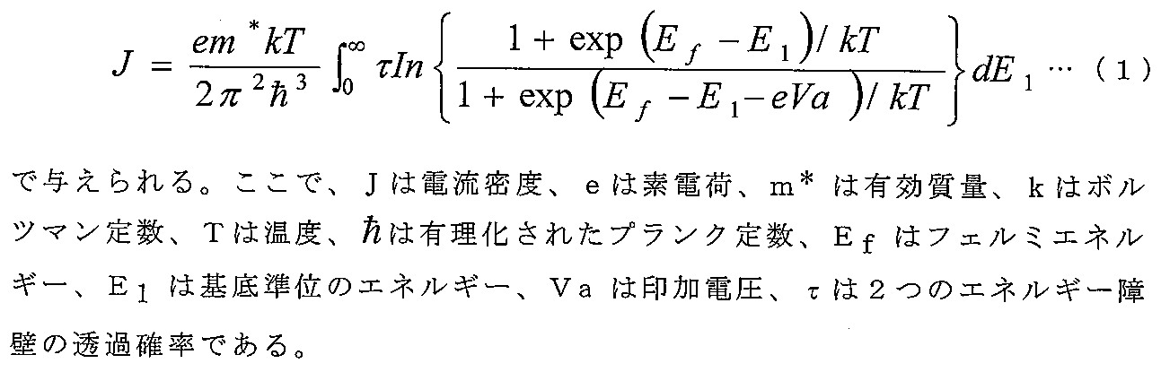
なお、これらの関係は、参考文献1(K. F. Brennan, and C. J. Summers, “Theory of resonant tunneling in a variably spaced multiquantum well structure: An Airy function approach”, Journal of Applied Physics 61 614 (1987).)及び参考文献2(M. O. Vassell, J. Lee, and H. F. Lockwood, “Multibarrier tunneling in Ga1-xAlxAs/GaAs heterostructures”, Journal of Applied Physics 54 5206)に詳しく説明されている。
前記(1)式から分かるよう、電流は、透過確率τを電子のエネルギーの関数で重み付けした積分で与えられ、透過確率τの特性が、電流・電圧特性に大きく影響する。透過確率τの計算については、様々な方法が提案されている(参考文献1,2)。
図9に、参考文献2が提案する方法で計算した、本実施形態に係わる半導体装置における透過確率τと前記電極領域151から入力される電子のエネルギーの関係を、印加電圧が小さい場合について示す。図9で、電子のエネルギーが増加すると、透過確率τが、初めは増加するものの、16meVを境に減少している。これは、本実施形態に係わる半導体装置において、チャネル領域110内の基底準位GSが、電子供給源である電極領域151のフェルミエネルギーよりもエネルギー的に低くなるために、電子の透過確率τが減少することに対応している。即ち、本実施形態の半導体装置において、負性微分抵抗特性が発現する。
ここで、室温動作を可能にするためには、チャネル領域110中での量子化された基底準位GSと第一励起準位EL1のエネルギー差は、室温の熱エネルギーである25meV以上であることが必要である。この25meVのエネルギー差を得るには、チャネル領域110のSiの厚さが、7nm以下であることが必要条件となる。
また、室温動作を可能にするには、チャネル領域110とチャネル領域111,112の基底準位のエネルギー差を、少なくとも25meV以上にする必要がある。このためには、チャネル領域110とチャネル領域111,112のSiの厚さに以下の関係があることが必要となる。

図10に、図8に示す素子に電圧を印加した場合の電流・電圧特性を示し、図11(a)~(c)に、各電圧印加状態でのエネルギーバンド構造を示す。図10のAの電圧が印加された状態では、図11(a)に示すように、チャネル領域110内の基底準位が、電子の供給源であるチャネル領域111内の電子の代表的なエネルギーであるフェルミエネルギーとエネルギー的に近くなるため、電流が流れ始める。
図10のBの電圧が印加された状態では、図11(b)に示すように、より多くの電子が、チャネル領域110に供給されるため、図11(a)の状態と比べて、電流が増加する。さらに印加電圧を上げ、図10のCの電圧が印加された状態では、図11(c)に示すように、チャネル領域110内の基底準位が、チャネル領域111内のフェルミエネルギーよりも、エネルギー的に低くなる。図11(c)の状態では、チャネル領域111から供給される電子を受け入れるエネルギー準位が、チャネル領域110内に存在しないので、電流は流れにくくなる。よって、図11(b)の電圧印加状態と図11(c)の電圧印加状態の間では、電圧を増加すると電流が減少するという負性微分抵抗特性が発現することになる。
上述のように、負性微分抵抗特性を発現するためには、2つの電子に対するエネルギー障壁と、その間に存在するエネルギー準位が量子化された領域、また、エネルギー障壁に隣接する電子の供給源が必要である。
次に、本実施形態に係わる半導体装置の製造プロセスについて、図12(a)(b)~図15(a)(b)を参照して説明する。
ここで、本実施形態の半導体装置の製造プロセスが、従来のMOSFETの製造プロセスと整合性が良く、従来のMOSFETと同一ウエハ内に混載が可能であることを示すため、MOSFETの製造プロセスと対比させて説明する。図12~図15中の(a)は本実施形態、(b)は従来のMOSFETである。
まず、図12(a)(b)に示すように、Si基板100上に埋め込み絶縁膜101を介してSi層(SOI層)105を形成したSOI基板を用意する。そして、図12(a)に示すように、本実施形態に係わる半導体装置が製造される領域のSOI層105を薄膜化する。このとき、MOSFETが製造される領域のSOI層105の薄膜化を行うことも可能であるが、本実施形態では、図12(b)に示すように薄膜化を行わない場合について説明する。
続いて、本実施形態の半導体装置をその周辺に製造される他の半導体装置と電気的に分離するため、本実施形態の半導体装置に使用するSOI層105の周辺領域を除去する。
次いで、図13(a)に示すように、薄い絶縁膜と金属若しくはポリSiからなる導電膜とを堆積した後に、RIE(Reactive Ion Etching)で選択エッチングすることにより、ゲート絶縁膜120及びゲート電極130を形成する。この際、ゲート電極130の下に位置するチャネル領域110のSiの厚さが、上部にゲート電極130が存在しないSOI層のSiの厚さよりも厚くなるようにする。その後、上部にゲート電極130が存在しないSOI層表面に酸化膜(図示せず)を形成し、薬液によるウェトエッチング(Wet Etching)によりこの酸化膜を剥離する。酸化膜を形成した後に剥離するのは、上部にゲート電極130が存在しないSOI層表面を平坦化するためである。
本実施形態の半導体装置のゲート絶縁膜120とゲート電極130の形状加工と、酸化膜の形成及び剥離を行う際には、同一ウエハに混載される周辺領域のMOSFETは、マスク等を使用することで保護される。酸化膜の剥離終了後、本実施形態の半導体装置をマスク等で保護し、周辺領域のMOSFETのゲート加工、及び所望の不純物打ち込みを行う。これにより、図13(b)に示すように周辺領域では、絶縁膜の加工によりゲート絶縁膜125が形成され、導電膜の加工によりゲート電極135が形成される。そして、不純物の打ち込みによりソース/ドレイン領域(図示せず)が形成されることになる。その後、本実施形態の半導体装置を保護しているマスク等を除去する。
次いで、図14(a)(b)に示すように、ゲート電極130,135の側面に、側壁絶縁膜140を形成する。この工程は、本実施形態の半導体装置及び周辺領域のMOSFETで同時に行う。
次いで、図15(a)(b)に示すように、上部に側壁絶縁膜140が存在しないSOI領域上にSiの積み増しを行い、電極領域151,152を形成する。さらに、電極領域151,152に、砒素(As)や燐(P)等の不純物の導入、不純物活性化アニールを行うことで、電極領域151,152を、電気伝導率の高いn型Siとする。本実施形態の半導体装置の電極領域151,152が形成される際には、同様の工程が、周辺領域のMOSFETに対しても行われるが、MOSFETの性能が劣化することはないので、問題とならない。
この後は、周辺領域のMOSFET製造に用いられている配線工程により、本実施形態の半導体装置への外部からの電気的アクセスを可能にする。
本実施形態では、ゲート絶縁膜120及びゲート電極130を、それぞれ、同一ウエハに混載されるMOSFETのゲート絶縁膜125及びゲート電極135と同じ材料にすることで、製造プロセスが簡略化される。つまり、本実施形態に係わる半導体装置の製造プロセスは、従来のMOSFETの製造プロセスとの整合性が良く、従来のMOSFETと同一ウエハに混載することが容易である。
このように本実施形態の半導体装置では、SOIウエハ上に作製された2つの電極領域151,152を有し、電極領域151,152間のSOI層を、片方の電極領域151からもう片方の電極領域152に向かって、SOI層のウエハ面直方向のSiの厚さによって、次のように3つの領域に区分する。1つ目のSOI層領域(第2のチャネル領域)111、及び3つ目のSOI層領域(第2のチャネル領域)112のウエハ面直方向のSiの厚さを、2つ目のSOI層領域(第1のチャネル領域)110のウエハ面直方向のSiの厚さよりも薄くし、且つSOI層領域110上に絶縁膜120を形成し、SOI層領域111,112上に絶縁膜140を形成する。
ここで、2つの電極領域151,152を、それぞれ従来のMOSFETのソース領域とドレイン領域で代用し、SOI層領域110上の絶縁膜をゲート絶縁膜、SOI層領域111,112上の絶縁膜をゲート横に形成する側壁で代用すれば、従来のMOSFETを製造するSiベースの製造プロセスと整合性良く製造することが可能であり、従来のMOSFETを同一ウエハに混載することが容易となる。
(第2の実施形態)
次に、本発明の第2の実施形態に係わる半導体装置について説明する。本実施形態は、第1の実施形態の半導体装置(負性微分抵抗素子)と、トランジスタ及びキャパシタを組み合わせることで、メモリ動作の機能を有するRT-SRAMを構成したものである。
次に、本発明の第2の実施形態に係わる半導体装置について説明する。本実施形態は、第1の実施形態の半導体装置(負性微分抵抗素子)と、トランジスタ及びキャパシタを組み合わせることで、メモリ動作の機能を有するRT-SRAMを構成したものである。
図16に示すように、ビット線BLとワード線WLの交差部にメモリセルとして機能するRT-SRAMが形成されている。MOSトランジスタ201のゲート電極はワード線WLに接続され、ソース/ドレイン領域の一方はビット線に接続され、ソース/ドレイン領域の他方はキャパシタ202を介して接地端に接続されている。このようなDRAMの基本構成に加え、第1の実施形態の負性微分抵抗素子211,212が設けられている。
即ち、MOSトランジスタ201とキャパシタ202の接続点であるストレージノード(SN)に第1の負性微分抵抗素子211の一方の電極領域が接続され、負性微分抵抗素子211の他方の電極領域は所望の電圧Vref を保持するように外部の電子回路と接続されている。SNに第2の負性微分抵抗素子212の一方の電極領域が接続され、負性微分抵抗素子212の他方の電極領域は所望の電圧Vssを保持するように外部の電子回路と接続されている。ここで、Vrefは、Vssよりも高い電位である。
上記の構造により、図16中のストレージノード(SN)に、2つの異なる電位を、リフレッシュ動作することなく保持することが可能となる。次に、上述の構造により、SNに、2つの異なる電位をリフレッシュ動作無しに保持することが可能となる機構を説明する。
説明を簡単にするため、SNの電位がVref である状態を「1」の状態、SNの電位がVssである状態を「0」の状態と呼ぶことにする。以下では、例として、初期状態が「0」である場合に「1」を書き込み、一定時間後に「1」を読み出す場合を例に説明する。
まず、ワード線WL、ビット線BLの電位を上げて、MOSFET201のゲートに電圧を印加することで、MOSFET201のソース/ドレイン領域間を電気的に導通状態にし、SNに「1」を書き込む。その後、ワード線WLの電位を下げて、MOSFET201のソース/ドレイン領域間を電気的に不導通の状態にする。SNの電位がVref であるので、負性微分抵抗素子211に電流は流れない。また、Vref-Vss=Vvalley となるように電位を設定すれば、負性微分抵抗素子212にも電流は流れない。ここで、Vvalley は、前記図10中のC点に相当する電位である。そのため、SNに「1」が保持される。SNが「1」の状態を保持している間、SNに蓄積された電荷がリークにより減少するので、SNの電位は低下する。
従来のDRAMでは、一定時間後にリフレッシュ動作を行うことで、SNの電位を再度高くする必要がある。しかし、本実施形態に係わる半導体装置では、SNの電位が低下すると、SNとVref 間に電圧が生じるため、負性微分抵抗素子211に電流が流れ、SNの電位が再びVref に戻される。負性微分抵抗素子211に電流が流れることで、SNの電位が再びVref に戻されるという動作は、リーク電流が、負性微分抵抗素子211に流れる電流よりも小さい場合において成立する。このため、本実施形態の半導体装置では、リフレッシュ動作無しに、SNに長時間「1」を保持することが可能である。
また、SNに保持されている情報の読み出しは、ワード線WLの電位を上げ、MOSFET201のソース/ドレイン領域間を電気的に導通状態にし、SNに蓄積された電荷を、ビット線BLを通して増幅器に入力することで行う。
逆に、SNに「0」を保持する場合に、宇宙線等のソフトエラーで、SNの電位が上がると、負性微分抵抗素子212に電圧が印加されることになるので、SNの電位は再びVssに戻されることになる。
このように本実施形態の半導体装置では、リフレッシュ動作を必要としないメモリ機能を実現することが可能である。
上記の実施形態はあくまで、例として挙げたものであり、本発明を限定するものではない。また、例えば、実施形態の応用例としては、以下に示す、第3の実施形態、第4の実施形態、及び第5の実施形態のような実施形態もある。以下に示す、第3~第5の実施形態は、第1の実施形態の応用形態の一例であり、第1の実施形態の設計例の範囲内に含まれる。
(第3の実施形態)
図17は、本発明の第3の実施形態に係わる半導体装置の素子構造を示す断面図であり、前記図2と同様にチャネル長方向に沿った断面を示している。なお、図中の300,310,311,312,320,330,340,351,352,370,371,372は、図2中の100,110,111,112,120,130,140,151,152,170,171,172にそれぞれ対応している。
図17は、本発明の第3の実施形態に係わる半導体装置の素子構造を示す断面図であり、前記図2と同様にチャネル長方向に沿った断面を示している。なお、図中の300,310,311,312,320,330,340,351,352,370,371,372は、図2中の100,110,111,112,120,130,140,151,152,170,171,172にそれぞれ対応している。
本実施形態の半導体装置は、埋め込み絶縁膜301の形状が異なること以外は、第1の実施形態と同様であるので、第1の実施形態と同様である部分の説明は省略する。
本実施形態の半導体装置では、埋め込み絶縁膜301は、第1のチャネル領域310、第2のチャネル領域311,312、及び電極領域351,352の下にのみ存在する。埋め込み絶縁膜301が、チャネル領域310,311,312、及び電極領域351,352の下にのみ存在する構造では、後述するように、バルクシリコンウエハ300を利用することが可能である。従って、バルクシリコンウエハ300上に製造した周辺回路と混載することが可能となる。一般に、バルクシリコンウエハは、SOIウエハに比べて、安価であるため、後述するように、製造プロセスが複雑になるが、材料費を安価にすることが可能である。
次に、本実施形態の半導体装置の製造プロセスについて説明する。
まず、図18(a)に示すように、Si基板300の表面部に、STI(Shallow Trench Isolation)、若しくはLOCOS(Local Oxidation of Silicon)を用いて、半導体装置が製造されるSi領域を周辺のSi領域と電気的に分離するための素子分離絶縁膜360を形成する。続いて、素子分離絶縁膜360で囲まれたSi領域の表面近傍のSiを除去した後、SiGe層303をエピタキシャル成長し、その上にSi層305をエピタキシャル成長する。
次いで、図18(b)に示すように、薄い絶縁膜と金属若しくはポリシリコンからなる導電膜とを堆積した後に、これらを選択エッチングすることにより、ゲート絶縁膜320及びゲート電極330を形成する。また、ゲート絶縁膜320及びゲート電極330を加工する際、ゲート電極膜330の下に位置する第1のチャネル領域310のSiの厚さが、上部にゲート電極膜330が存在しない第2のチャネル領域311,312の厚さよりも厚くなるようにする。
次いで、図18(c)に示すように、SiGe層303を薬液で除去した後、SiGe層303が除去されてできた空洞に、酸化膜からなる埋め込み絶縁膜301を形成する。SiGe層303が除去されても、Si層305(チャネル領域310,311,312)は、ゲート絶縁膜320及びゲート電極膜330により支えられるので、下に落ちることはない。また、SiGe層303の除去及び埋め込み絶縁膜301の形成は、本実施形態の半導体装置を周辺から電気的に分離しているSTI、若しくはLOCOSの一部分に、ウエハ面直方向の穴を開けることで行う。
続いて、第2のチャネル領域311,312の表面に酸化膜を形成した後、薬液によるウェトエッチングによりこの酸化膜を剥離する。酸化膜を形成した後に剥離するのは、上部にゲート電極材料膜330が存在しないSi層の表面を平坦化するためである。
これ以降は、先の第1の実施形態と同様に、側壁絶縁膜340の形成、更に電極領域351,352等の形成を行うことにより、前記図17に示す構造が得られる。
(第4の実施形態)
図19乃至図21は、本発明の第4の実施形態に係わる半導体装置の素子構造を説明するためのもので、図19は平面図、図20は図19の矢視III-III方向断面図、図21は図19の矢視IV-IV方向断面図である。
図19乃至図21は、本発明の第4の実施形態に係わる半導体装置の素子構造を説明するためのもので、図19は平面図、図20は図19の矢視III-III方向断面図、図21は図19の矢視IV-IV方向断面図である。
なお、図19~21中の400,410,411,412,420,430,440,451,452,470,471,472は、図2及び図3中の100,110,111,112,120,130,140,151,152,170,171,172にそれぞれ対応している。
基本的な構造は第1の実施形態と同様であるが、本実施形態では、電極領域451と電極領域452との間に存在するSOI層からなる電流路を複数本にしている。図19では、一例として、SOI層からなる電流路が3本の場合を示している。
図20では、第1のチャネル領域410の断面が四角形になっているが、断面形状は任意であり、必ずしも四角形である必要はない。本実施形態の半導体装置は、SOIウエハ上に製造される。第1のチャネル領域410、第2のチャネル領域411,412は、図21に示すように、電極領域451と電極領域452との間に流れる電流方向と垂直の全方向について、ゲート絶縁膜420、及び埋め込み絶縁膜401により囲まれている。また、ゲート絶縁膜420は、ゲート電極膜430により囲まれている。また、ウエハ面内方向であり、且つ電極領域451と電極領域452との間に流れる電流方向と垂直な方向の、チャネル領域410の長さは、ウエハ面垂直方向のチャネル領域410の長さの1.7倍程度であることが望ましい。
上述したように、室温での負性微分抵抗特性の発現を容易にするためには、チャネル領域410内のエネルギー準位が、顕著に量子化されていることが望ましい。本実施形態の半導体装置では、チャネル領域410が、ゲート絶縁膜420及び埋め込み絶縁膜401により囲まれているため、チャネル領域410内の電子には、電極領域451と電極領域452との間に流れる電流方向と垂直な全方向に渡って、量子閉じ込め効果が作用する。そのため、第1の実施形態に比べて、チャネル領域410内のエネルギー準位の量子化が、より顕著に起こる。また、一般に、半導体装置は(001)面のSiウエハ上に製造されるため、本実施形態の半導体装置が、(001)面のSOIウエハ上に製造されることが、従来の製造プロセスを踏襲できるため、望ましい。
本実施形態の半導体装置が、(001)面のSOIウエハ上に製造されると、ウエハ面内方向であり、且つ電極領域451と電極領域452との間に流れる電流方向と垂直な方向は、<110>方向となる。Siの<110>方向には、0.315m0 と0.19m0 の2種類の電子の有効質量がある。ここで、m0 は真空中での電子の質量である。<110>方向の大きい方の有効質量0.315m0 は、ウエハ面直方向である<001>方向の2種類の有効質量である0.91m0 と0.19m0 のうち、大きい方の有効質量0.91m0 の1/3程度である。
一般に、量子閉じ込め効果の強さは、有効質量に反比例し、閉じ込め方向の厚さの2乗に反比例する。そのため、<110>方向のSiの膜厚が、<001>方向のSiの膜厚の1.7倍程度であると、<110>方向と、<001>方向で、2種類の有効質量のうち大きい有効質量をした電子に対して、同じ強さの量子閉じ込め効果が働く。<110>方向のSiの膜厚が、<001>方向のSiの膜厚の1.7倍程度よりも薄くなると、<110>方向の量子閉じ込め効果が、<001>方向の量子閉じ込め効果よりも大きくなり、全体的なエネルギー準位を決定する主たる要因となる。
上述のように、<110>方向の2種類の有効質量同士は、<001>方向の場合と比べて値が近いため、1つの有効質量に注目すれば、量子化されたエネルギー準位の伝導帯下端からのエネルギー増加量は大きい。しかし、異なる有効質量に起因した量子化されたエネルギー準位間のエネルギー分裂量は、<001>方向の場合と比較すると小さい。そのため、<110>方向の量子閉じ込め効果が、全体的なエネルギー準位を決定する主たる要因となると、チャネル領域410内の量子化されたエネルギー準位間の小さなエネルギー分裂量が、負性微分抵抗特性の発現に不利に作用することになる。
また、逆に、<110>方向の膜厚が、<001>方向のSiの膜厚の1.7倍程度よりも厚くなると、<110>方向の量子閉じ込め効果が弱くなる。よって、ウエハ面内方向であり、且つ電極領域451と電極領域452との間に流れる電流方向と垂直な方向のチャネル領域410の長さは、ウエハ面垂直方向のチャネル領域410の長さの1.7倍程度であることが望ましい。
本実施形態に係わる半導体装置は、第1の実施形態の製造プロセスと同様の製造プロセスで製造することが可能であるため、本実施形態の半導体装置の製造プロセスの説明は省略する。
(第5の実施形態)
本実施形態では、先に説明した第4の実施形態の半導体装置の構成において、SOI基板の代わりにバルクSi基板を用いた。この場合、Si層を複数本に形成する以外は、第3の実施形態と同様の方法で作製することができる。埋め込み絶縁膜の形状が異なること以外は、第4の実施形態の半導体装置と同様であり、第4の実施形態の図19に対応する断面図は前記図17と同じとなる。
本実施形態では、先に説明した第4の実施形態の半導体装置の構成において、SOI基板の代わりにバルクSi基板を用いた。この場合、Si層を複数本に形成する以外は、第3の実施形態と同様の方法で作製することができる。埋め込み絶縁膜の形状が異なること以外は、第4の実施形態の半導体装置と同様であり、第4の実施形態の図19に対応する断面図は前記図17と同じとなる。
このようにすれば、第4の実施形態と同様の効果が得られるのは勿論のこと、第3の実施形態と同様に、バルクSiウエハ上に製造した周辺回路と混載することが可能となり、材料費を安価にすることが可能である。
(付記)
本発明の特徴的な構成は(請求の範囲)に示すが、それ以外にも、次のような特徴を有する。
本発明の特徴的な構成は(請求の範囲)に示すが、それ以外にも、次のような特徴を有する。
(1) チャネル領域を流れる電流の担い手が電子である。
(2) 第1のチャネル領域のチャネル長方向の長さは10nm以下である。
(3) 2つの電極領域間を流れる電流の方向と垂直の全方向に関して、第1及び第2のチャネル領域が絶縁膜により囲まれており、且つ2つの電極領域間を流れる電流の方向と垂直の方向に関して、第1及び第2のチャネル領域を囲む絶縁膜の外周の1/2以上が、ゲート電極材料膜により囲まれている。
(4) 第1及び第2のチャネル領域が形成されているSi領域下の絶縁膜が、ウエハ面内全領域に渡って存在する。
(5) 第1及び第2のチャネル領域が形成されているSi領域下の絶縁膜が、チャネル領域、及び電極領域下にのみ存在する。
また、製造方法としての特徴的な工程は次の通りである。
(1) 絶縁膜上に、第1のチャネル領域、該チャネル領域を一方向から挟む第2のチャネル領域、及び第1及び第2のチャネル領域を前記一方向から挟む電極領域とすべきSi層を形成する工程
(2) Si層上の前記第1のチャネル領域とすべき部分上にゲート絶縁膜を介してゲート電極を形成する工程
(3) ゲート電極をマスクに用いてSi層を一部エッチングすることにより、第2のチャネル領域とすべき部分及び前記電極領域とすべき部分のSi層を薄くする工程
(4) ゲート電極の側壁及びSi層の前記第2のチャネル領域とすべき部分上に側壁絶縁膜を形成する工程
(5) ゲート電極又は側壁絶縁膜で覆われていないSi層上に新たにSi層を成長することにより、電極領域とすべき部分のSi層の厚さを第1のチャネル領域とすべき部分のSiの厚さよりも厚くする工程
(変形例)
なお、本発明は上述した各実施形態に限定されるものではない。実施形態の説明においては、半導体装置、半導体装置の製造プロセス等で、本発明の説明に直接必要としない部分等については記載を省略したが、必要とされる半導体装置、半導体装置の製造プロセス等に関わる要素を適宜選択して用いることができる。
(2) Si層上の前記第1のチャネル領域とすべき部分上にゲート絶縁膜を介してゲート電極を形成する工程
(3) ゲート電極をマスクに用いてSi層を一部エッチングすることにより、第2のチャネル領域とすべき部分及び前記電極領域とすべき部分のSi層を薄くする工程
(4) ゲート電極の側壁及びSi層の前記第2のチャネル領域とすべき部分上に側壁絶縁膜を形成する工程
(5) ゲート電極又は側壁絶縁膜で覆われていないSi層上に新たにSi層を成長することにより、電極領域とすべき部分のSi層の厚さを第1のチャネル領域とすべき部分のSiの厚さよりも厚くする工程
(変形例)
なお、本発明は上述した各実施形態に限定されるものではない。実施形態の説明においては、半導体装置、半導体装置の製造プロセス等で、本発明の説明に直接必要としない部分等については記載を省略したが、必要とされる半導体装置、半導体装置の製造プロセス等に関わる要素を適宜選択して用いることができる。
その他、本発明の要素を具備し、当業者が適宜設計変更しうる全ての半導体装置は、本発明の範囲に包含される。本発明の範囲は、特許請求の範囲及びその均等物の範囲によって定義されるものである。
100,300,400…支持基板(半導体基板)
101,301,401…埋め込み絶縁膜
105…SOI層
110,310,410…第1のチャネル領域
111,112,311,312,411,412…第2のチャネル領域
120,125,320,420…ゲート絶縁膜
130,135,330,430…ゲート電極
140,340,440…側壁絶縁膜
151,152,351,352,451,452…電極領域
160…絶縁膜
170,370,470…層間絶縁膜
171,172,371,372,471,472…プラグ電極
201…MOSトランジスタ
202…キャパシタ
211…第1の負性微分抵抗素子
212…第2の負性微分抵抗素子
303…SiGe層
305…Si層
360…素子分離絶縁膜
101,301,401…埋め込み絶縁膜
105…SOI層
110,310,410…第1のチャネル領域
111,112,311,312,411,412…第2のチャネル領域
120,125,320,420…ゲート絶縁膜
130,135,330,430…ゲート電極
140,340,440…側壁絶縁膜
151,152,351,352,451,452…電極領域
160…絶縁膜
170,370,470…層間絶縁膜
171,172,371,372,471,472…プラグ電極
201…MOSトランジスタ
202…キャパシタ
211…第1の負性微分抵抗素子
212…第2の負性微分抵抗素子
303…SiGe層
305…Si層
360…素子分離絶縁膜
Claims (6)
- 絶縁膜上に設けられ、Siで形成された第1のチャネル領域と、
前記第1のチャネル領域を挟んで前記絶縁膜上にそれぞれ設けられ、前記第1のチャネル領域よりも膜厚の薄いSiで形成された2つの第2のチャネル領域と、
前記第1及び第2のチャネル領域を挟んで前記絶縁膜上に設けられ、且つ前記第2のチャネル領域に対して前記第1のチャネル領域と反対側にそれぞれ設けられ、前記第1のチャネル領域よりも膜厚の厚いSiで形成された2つの電極領域と、
を具備し、
前記電極領域間への電圧の印加により、前記電極領域間に負性微分抵抗特性を発現させることを特徴とする半導体装置。 - スイッチング用トランジスタ及びキャパシタが接続されるストレージノードと第1の電位端との間に負性微分抵抗特性を有する第1の負性微分抵抗素子を接続し、且つ前記ストレージノードと第2の電位端との間に負性微分抵抗特性を有する第2の負性微分抵抗素子を接続した半導体装置であって、
前記各負性微分抵抗素子はそれぞれ、
半導体基板上に形成された絶縁膜上に設けられ、Siで形成された第1のチャネル領域と、
前記第1のチャネル領域を挟んで前記絶縁膜上にそれぞれ設けられ、前記第1のチャネル領域よりも膜厚の薄いSiで形成された2つの第2のチャネル領域と、
前記第1及び第2のチャネル領域を挟んで前記絶縁膜上に設けられ、且つ前記第2のチャネル領域に対して前記第1のチャネル領域と反対側にそれぞれ設けられ、前記第1のチャネル領域よりも膜厚の厚いSiで形成された2つの電極領域と、
を具備したことを特徴とする半導体装置。 - 前記第1のチャネル領域上にゲート絶縁材料膜を介して金属又はポリSiで形成されるゲート電極材料膜が設けられ、前記ゲート電極材料膜の側面及び前記第2のチャネル領域上に側壁絶縁膜が設けられていることを特徴とする請求項2記載の半導体装置。
- 前記半導体基板には、前記第1,第2のチャネル領域及び前記電極領域が設けられる領域とは別の領域に電界効果型トランジスタが設けられ、
前記ゲート電極材料膜は前記電界効果型トランジスタのゲート電極の材料と同じであり、前記ゲート絶縁材料膜は前記電界効果型トランジスタのゲート絶縁膜の材料と同じであり、且つ前記側壁絶縁膜は前記電界効果型トランジスタのゲート側壁絶縁膜の材料と同じであることを特徴とする請求項3記載の半導体装置。 - 前記半導体基板はSi基板であり、前記第1のチャネル領域及び前記半導体基板には、同種の不純物が同濃度で含有されていることを特徴とする請求項2記載の半導体装置。
- 前記第1のチャネル領域の膜厚T1 は7nm以下であり、円周率をπ、eを素電荷、ウエハ面直方向のSiの有効質量をm* としたとき、前記膜厚T1 と前記第2のチャネル領域の膜厚T2 との間に、

Priority Applications (1)
| Application Number | Priority Date | Filing Date | Title |
|---|---|---|---|
| PCT/JP2009/061769 WO2010150407A1 (ja) | 2009-06-26 | 2009-06-26 | 半導体装置 |
Applications Claiming Priority (1)
| Application Number | Priority Date | Filing Date | Title |
|---|---|---|---|
| PCT/JP2009/061769 WO2010150407A1 (ja) | 2009-06-26 | 2009-06-26 | 半導体装置 |
Publications (1)
| Publication Number | Publication Date |
|---|---|
| WO2010150407A1 true WO2010150407A1 (ja) | 2010-12-29 |
Family
ID=43386200
Family Applications (1)
| Application Number | Title | Priority Date | Filing Date |
|---|---|---|---|
| PCT/JP2009/061769 Ceased WO2010150407A1 (ja) | 2009-06-26 | 2009-06-26 | 半導体装置 |
Country Status (1)
| Country | Link |
|---|---|
| WO (1) | WO2010150407A1 (ja) |
Cited By (3)
| Publication number | Priority date | Publication date | Assignee | Title |
|---|---|---|---|---|
| FR3033665A1 (fr) * | 2015-03-11 | 2016-09-16 | Commissariat Energie Atomique | Transistor a electron unique et son procede de realisation |
| EP3660921A1 (fr) * | 2018-12-02 | 2020-06-03 | Commissariat à l'énergie atomique et aux énergies alternatives | Procédé de fabrication d'un composant électronique à multiples îlots quantiques et composant électronique résultant |
| JP2021061443A (ja) * | 2013-08-30 | 2021-04-15 | 株式会社半導体エネルギー研究所 | 半導体装置 |
Citations (4)
| Publication number | Priority date | Publication date | Assignee | Title |
|---|---|---|---|---|
| JPS5961967A (ja) * | 1982-09-30 | 1984-04-09 | インタ−ナシヨナル ビジネス マシ−ンズ コ−ポレ−シヨン | 半導体装置 |
| JPS62154668A (ja) * | 1985-12-27 | 1987-07-09 | Toshiba Corp | 半導体装置 |
| JPH09260690A (ja) * | 1996-03-25 | 1997-10-03 | Toshiba Corp | 半導体装置及び半導体集積回路 |
| JPH10189888A (ja) * | 1996-10-22 | 1998-07-21 | Matsushita Electric Ind Co Ltd | 半導体装置及びその製造方法 |
-
2009
- 2009-06-26 WO PCT/JP2009/061769 patent/WO2010150407A1/ja not_active Ceased
Patent Citations (4)
| Publication number | Priority date | Publication date | Assignee | Title |
|---|---|---|---|---|
| JPS5961967A (ja) * | 1982-09-30 | 1984-04-09 | インタ−ナシヨナル ビジネス マシ−ンズ コ−ポレ−シヨン | 半導体装置 |
| JPS62154668A (ja) * | 1985-12-27 | 1987-07-09 | Toshiba Corp | 半導体装置 |
| JPH09260690A (ja) * | 1996-03-25 | 1997-10-03 | Toshiba Corp | 半導体装置及び半導体集積回路 |
| JPH10189888A (ja) * | 1996-10-22 | 1998-07-21 | Matsushita Electric Ind Co Ltd | 半導体装置及びその製造方法 |
Cited By (6)
| Publication number | Priority date | Publication date | Assignee | Title |
|---|---|---|---|---|
| JP2021061443A (ja) * | 2013-08-30 | 2021-04-15 | 株式会社半導体エネルギー研究所 | 半導体装置 |
| JP7016972B2 (ja) | 2013-08-30 | 2022-02-07 | 株式会社半導体エネルギー研究所 | 半導体装置 |
| FR3033665A1 (fr) * | 2015-03-11 | 2016-09-16 | Commissariat Energie Atomique | Transistor a electron unique et son procede de realisation |
| US9911841B2 (en) | 2015-03-11 | 2018-03-06 | Commissariat à l'énergie atomique et aux énergies alternatives | Single-electron transistor and its fabrication method |
| EP3660921A1 (fr) * | 2018-12-02 | 2020-06-03 | Commissariat à l'énergie atomique et aux énergies alternatives | Procédé de fabrication d'un composant électronique à multiples îlots quantiques et composant électronique résultant |
| FR3089213A1 (fr) * | 2018-12-02 | 2020-06-05 | Commissariat à l'Energie Atomique et aux Energies Alternatives | Procédé de fabrication d’un composant électronique à multiples îlots quantiques |
Similar Documents
| Publication | Publication Date | Title |
|---|---|---|
| US8227864B2 (en) | CMOS semiconductor device | |
| US12243913B2 (en) | Self-aligned backside contact integration for transistors | |
| JP4294935B2 (ja) | 半導体装置 | |
| US7952162B2 (en) | Semiconductor device and method for manufacturing the same | |
| US7301206B2 (en) | Semiconductor-on-insulator SRAM configured using partially-depleted and fully-depleted transistors | |
| CN111542924B (zh) | 集成组合件及形成集成组合件的方法 | |
| JP5775065B2 (ja) | 明白に異なる閾値電圧を有するトランジスタを持つsoiから製造する集積回路 | |
| KR102426245B1 (ko) | 반도체 디바이스 및 방법 | |
| US20200035686A1 (en) | Two port sram cell using complementary nano-sheet/wire transistor devices | |
| US7605447B2 (en) | Highly manufacturable SRAM cells in substrates with hybrid crystal orientation | |
| JP2009212413A (ja) | 半導体装置及び半導体装置の製造方法 | |
| JP2011503864A (ja) | 縦型多チャネル構造を有するトランジスタを備えたsramメモリセル | |
| JP7532730B2 (ja) | Sramセル構造 | |
| JP2014222740A (ja) | 半導体記憶装置 | |
| CN105023924A (zh) | 存储器件及其制造方法 | |
| US8946802B2 (en) | Method of eDRAM DT strap formation in FinFET device structure | |
| US20240006313A1 (en) | Self-aligned backside connections for transistors | |
| JP2009246383A (ja) | 半導体装置 | |
| US10418368B1 (en) | Buried local interconnect in source/drain region | |
| US20090224304A1 (en) | Soft error protection structure employing a deep trench | |
| US9012957B2 (en) | MOS transistor | |
| KR102220032B1 (ko) | 폴리 실리콘 이미터 층이 삽입된 2-단자 바이리스터 및 그 제조 방법 | |
| US20040164338A1 (en) | Semiconductor device and method for fabricating the same | |
| US20250142907A1 (en) | Semiconductor device including vertical channel having tube shape | |
| US12433020B2 (en) | Multi-VT solution for replacement metal gate bonded stacked FET |
Legal Events
| Date | Code | Title | Description |
|---|---|---|---|
| 121 | Ep: the epo has been informed by wipo that ep was designated in this application |
Ref document number: 09846538 Country of ref document: EP Kind code of ref document: A1 |
|
| NENP | Non-entry into the national phase |
Ref country code: DE |
|
| 122 | Ep: pct application non-entry in european phase |
Ref document number: 09846538 Country of ref document: EP Kind code of ref document: A1 |
|
| NENP | Non-entry into the national phase |
Ref country code: JP |