WO2010147178A1 - 発光装置および発光装置モジュール - Google Patents
発光装置および発光装置モジュール Download PDFInfo
- Publication number
- WO2010147178A1 WO2010147178A1 PCT/JP2010/060285 JP2010060285W WO2010147178A1 WO 2010147178 A1 WO2010147178 A1 WO 2010147178A1 JP 2010060285 W JP2010060285 W JP 2010060285W WO 2010147178 A1 WO2010147178 A1 WO 2010147178A1
- Authority
- WO
- WIPO (PCT)
- Prior art keywords
- light
- light emitting
- mounting surface
- emitting device
- reflecting member
- Prior art date
- Legal status (The legal status is an assumption and is not a legal conclusion. Google has not performed a legal analysis and makes no representation as to the accuracy of the status listed.)
- Ceased
Links
Images



















Classifications
-
- H—ELECTRICITY
- H10—SEMICONDUCTOR DEVICES; ELECTRIC SOLID-STATE DEVICES NOT OTHERWISE PROVIDED FOR
- H10W—GENERIC PACKAGES, INTERCONNECTIONS, CONNECTORS OR OTHER CONSTRUCTIONAL DETAILS OF DEVICES COVERED BY CLASS H10
- H10W90/00—Package configurations
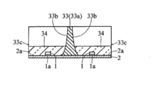
-
- H—ELECTRICITY
- H10—SEMICONDUCTOR DEVICES; ELECTRIC SOLID-STATE DEVICES NOT OTHERWISE PROVIDED FOR
- H10H—INORGANIC LIGHT-EMITTING SEMICONDUCTOR DEVICES HAVING POTENTIAL BARRIERS
- H10H20/00—Individual inorganic light-emitting semiconductor devices having potential barriers, e.g. light-emitting diodes [LED]
- H10H20/80—Constructional details
- H10H20/85—Packages
- H10H20/855—Optical field-shaping means, e.g. lenses
- H10H20/856—Reflecting means
-
- H—ELECTRICITY
- H10—SEMICONDUCTOR DEVICES; ELECTRIC SOLID-STATE DEVICES NOT OTHERWISE PROVIDED FOR
- H10W—GENERIC PACKAGES, INTERCONNECTIONS, CONNECTORS OR OTHER CONSTRUCTIONAL DETAILS OF DEVICES COVERED BY CLASS H10
- H10W72/00—Interconnections or connectors in packages
- H10W72/851—Dispositions of multiple connectors or interconnections
- H10W72/874—On different surfaces
- H10W72/884—Die-attach connectors and bond wires
-
- H—ELECTRICITY
- H10—SEMICONDUCTOR DEVICES; ELECTRIC SOLID-STATE DEVICES NOT OTHERWISE PROVIDED FOR
- H10W—GENERIC PACKAGES, INTERCONNECTIONS, CONNECTORS OR OTHER CONSTRUCTIONAL DETAILS OF DEVICES COVERED BY CLASS H10
- H10W90/00—Package configurations
- H10W90/701—Package configurations characterised by the relative positions of pads or connectors relative to package parts
- H10W90/751—Package configurations characterised by the relative positions of pads or connectors relative to package parts of bond wires
- H10W90/753—Package configurations characterised by the relative positions of pads or connectors relative to package parts of bond wires between laterally-adjacent chips
Definitions
- the present invention relates to a light emitting device and a light emitting device module.
- a light-emitting device including a light-emitting element such as a light-emitting diode element (LED) is known (for example, see Patent Document 1).
- a light-emitting element such as a light-emitting diode element (LED)
- LED light-emitting diode element
- an LED is mounted on a substrate, and the LED is sealed with a sealing member in that state.
- a reflection member having a frame-like light reflection surface is attached to the mounting surface of the substrate, and the periphery of the LED is completely surrounded by the light reflection surface of the reflection member. Surrounding.
- the present invention has been made to solve the above-described problems, and an object thereof is to provide a light-emitting device and a light-emitting device module capable of suppressing the occurrence of uneven brightness.
- a light-emitting device includes a light-emitting element that generates light, a base having an element mounting surface on which the light-emitting element is mounted, and an erected surface on the element mounting surface. And a reflecting member whose side surface is a light reflecting surface. When viewed from a direction parallel to the element mounting surface, one or more pairs of light extraction openings that face in opposite directions are formed on the wall of the reflecting member.
- the direction perpendicular to the element mounting surface (the standing direction of the wall portion of the reflecting member) and the vicinity thereof are simply referred to as the front direction
- the direction parallel to the element mounting surface ( The direction perpendicular to the standing direction of the wall portion of the reflecting member) and the vicinity thereof are simply referred to as the lateral direction.
- a pair of light extraction openings facing in opposite directions are formed in the wall of the reflecting member.
- a linear light source (light emitting device module) is produced by arranging the plurality of light emitting devices in a straight line, each of the plurality of light emitting devices is mutually connected. If only one set of a pair of light extraction openings facing in opposite directions is formed, and a plurality of light emitting devices are arranged so that the respective light extraction openings face each other, a region between adjacent light emission devices Can be suppressed from becoming dark. That is, it is possible to suppress the occurrence of luminance unevenness in the longitudinal direction of the linear light source (the light emitting device arrangement direction).
- an edge light type backlight for a liquid crystal display device, a fluorescent lamp, a light source for a scanner, and the like can be considered.
- a planar light source using a plurality of light emitting devices according to the first aspect for example, a backlight for a direct type liquid crystal display device
- a pair of light emitting devices facing each other in opposite directions is used. If two sets of light extraction openings are formed and a plurality of light emitting devices are arranged in a matrix so that the respective light extraction openings face each other, the occurrence of luminance unevenness can be suppressed.
- the light emitting device when viewed from a direction parallel to the element mounting surface, a region where the wall portion of the reflecting member is not erected and the wall portion of the reflecting member are notched in a concave shape Among the regions where at least one of the regions is provided, the region where the wall of the reflecting member is not erected, and the region where the wall of the reflecting member is cut into a concave shape It is preferable that at least one of the regions is an opening for light extraction. If comprised in this way, the opening part for light extraction for taking out light to a horizontal direction can be obtained easily.
- the light emitting device further includes a sealing member for sealing the light emitting element, and the sealing member is exposed from the light extraction opening. If comprised in this way, the light from the light emitting element sealed with the sealing member can be taken out laterally easily through the opening part for light extraction.
- the element mounting surface is formed in a quadrangular shape having two pairs of parallel sides, and at least one pair of the two pairs of sides of the element mounting surface. It is preferable that an opening for light extraction is disposed on each of the sides.
- a pair of sides that are orthogonal to the predetermined direction of the element mounting surface are not provided on each of the pair of sides parallel to the predetermined direction of the element mounting surface. If the opening for extracting light is arranged only in each of these, the directivity in the predetermined direction can be widened while the directivity in the direction orthogonal to the predetermined direction is kept narrow. Furthermore, if openings for light extraction are arranged on all the sides of the element mounting surface, the directivity in both the predetermined direction and the direction orthogonal to that direction can be expanded.
- the element mounting surface may be divided into two or more regions by a part of the wall portion of the reflecting member.
- a light emitting element is mounted in each of two or more regions on the element mounting surface.
- the height of a part of the wall portion of the reflecting member dividing the element mounting surface into two or more regions is The height of the other part of the wall of the reflecting member may be smaller. If comprised in this way, even if an element mounting surface is divided
- the wall thickness is set on a part of the wall portion of the reflecting member that divides the element mounting surface into two or more regions.
- a through hole penetrating in the direction may be formed.
- the light emitting element is preferably a light emitting diode element.
- the light emitting device module according to the second aspect of the present invention includes a plurality of light emitting devices according to the first aspect. If comprised in this way, generation
- the light extraction openings of the plurality of light emitting devices face each other. If comprised in this way, it will suppress that the area
- a plurality of light emitting devices may be linearly arranged. If comprised in this way, the linear light source with which generation
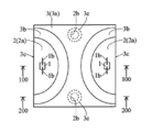
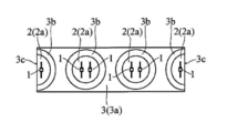
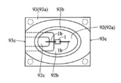
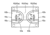
- FIG. 1 is a plan view of a light emitting device according to a first embodiment of the present invention.
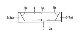
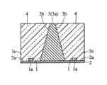
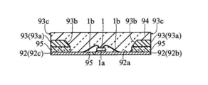
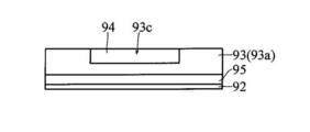
- FIG. 2 is a cross-sectional view taken along line 100-100 in FIG. It is a side view at the time of seeing from the A direction of FIG. It is a side view at the time of seeing from the B direction of FIG.
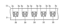
- It is a figure of the light-emitting device module using multiple light-emitting devices by 1st Embodiment.
- It is a figure of a fluorescent lamp.
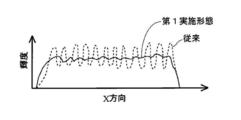
- It is a figure for demonstrating the effect of 1st Embodiment.
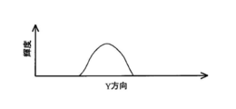
- It is a figure for demonstrating the effect of 1st Embodiment.
- It is a figure for demonstrating the manufacturing process of the light-emitting device by 1st Embodiment.
- FIG. 13 is a cross-sectional view taken along the line 100-100 in FIG.
- FIG. 13 is a cross-sectional view taken along line 200-200 in FIG.
- FIG. 16 is a cross-sectional view taken along the line 100-100 in FIG.
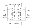
- FIG. 20 is a cross-sectional view taken along the line 100-100 in FIG. It is a side view at the time of seeing from A direction and B direction of FIG. It is a top view of the light-emitting device by the modification of 2nd Embodiment.
- FIG. 23 is a cross-sectional view taken along the line 100-100 in FIG.
- FIG. 25 is a cross-sectional view taken along line 100-100 in FIG. 24. It is a side view at the time of seeing from the B direction of FIG. It is a top view of the light-emitting device by 4th Embodiment of this invention.
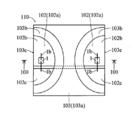
- FIG. 30 is a cross-sectional view taken along line 100-100 in FIG. 27. It is a side view at the time of seeing from the B direction of FIG. It is a top view of the light-emitting device by a 5th embodiment of the present invention.
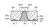
- FIG. 31 is a cross-sectional view taken along the line 100-100 in FIG. 30.
- FIG. 34 is a cross-sectional view taken along line 100-100 in FIG. 33. It is a side view at the time of seeing from the B direction of FIG. It is a side view of the light-emitting device by the modification of 6th Embodiment. It is a top view of the light-emitting device by a 7th embodiment of the present invention.
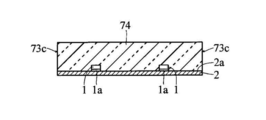
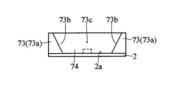
- FIG. 38 is a cross-sectional view taken along the line 100-100 in FIG. It is a side view at the time of seeing from the B direction of FIG.
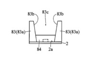
- FIG. 41 is a cross-sectional view taken along line 100-100 in FIG. 40. It is a side view at the time of seeing from the B direction of FIG. It is a side view of the light-emitting device by the modification of 8th Embodiment. It is a top view of the light-emitting device by 9th Embodiment of this invention.
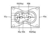
- FIG. 45 is a cross-sectional view taken along line 100-100 in FIG. 44. It is a side view at the time of seeing from A direction and B direction of FIG.
- FIG. 45 is a cross-sectional view taken along line 200-200 in FIG. 44.
- FIG. 52 is a cross-sectional view taken along line 100-100 in FIG. 51. It is a top view of the light-emitting device by the modification of 10th Embodiment.
- the light emitting device 10 of the first embodiment includes an LED 1 that generates light, a wiring board 2 on which the LED 1 is mounted, and a reflecting member 3 that reflects the light generated by the LED 1. And a sealing member 4 for sealing the LED 1 and the like.
- the LED 1 is an example of the “light emitting element” in the present invention
- the wiring board 2 is an example of the “base” in the present invention.
- the wiring board 2 on which the LED 1 is mounted is a glass epoxy board, and the LED mounting surface (element mounting surface) 2a is formed in a square shape.
- the LED 1 is mounted on the LED mounting surface 2a through the adhesive paste 1a.
- the wiring board 2 is provided with an electrode pattern (not shown), and the electrodes of the LED 1 are electrically connected via the wires 1b.
- the reflection member 3 is made of resin, metal, or the like as a constituent material, and is bonded and fixed to the LED mounting surface 2a. Further, the reflecting member 3 is formed in a shape that protrudes in a wall shape from the LED mounting surface 2a in a state where it is bonded and fixed to the LED mounting surface 2a. That is, the reflecting member 3 is composed of a wall portion 3a erected on the LED mounting surface 2a. The side surface of the wall 3a of the reflecting member 3 is inclined with respect to the LED mounting surface 2a, and the inclined side surface of the wall 3a of the reflecting member 3 is a light reflecting surface 3b.
- the pair of side end portions parallel to the predetermined direction has a wall portion of the reflecting member 3 extending from one end of the side end portion to the other end region. 3a is erected, but a pair of side end portions orthogonal to a predetermined direction has a region (opening portion 3c for light extraction) in which the wall portion 3a of the reflecting member 3 is opened without being erected. Is provided.
- the wall 3a of the reflecting member 3 is erected only on both end sides, and the light extraction opening 3c is provided on the center side. (See FIG. 4).
- each of the two light emitting regions has one light extraction opening (an opening region located on the side perpendicular to the predetermined direction of the LED mounting surface 2a) 3c.
- the planar shape of the light emitting region is a semicircular shape, and the light extraction opening 3c is arranged on the linear side.
- the LED 1 is sealed by the sealing member 4, but the sealing member 4 is exposed from the opening 3 c for extracting light.
- the pair of light extraction openings 3 c that face in opposite directions are formed on the reflecting member 3.
- the light reflected by the wall 3a of the reflecting member 3 and extracted in the front direction is reduced.
- light that is extracted in the lateral direction through the light extraction opening 3c is newly generated.
- a plurality of light emitting devices 10 according to the first embodiment are prepared, and the plurality of light emitting devices 10 are linearly mounted on the mounting substrate 5 to thereby form a light emitting device module (linear light source). ) 11, by arranging the plurality of light emitting devices 10 so that the respective light extraction openings 3 c face each other, it is possible to suppress darkening of the region between the adjacent light emitting devices 10. it can. Therefore, if this light emitting device module 11 is used as the light source of the fluorescent lamp 12 (see FIG. 6), as shown in FIG. 7, the occurrence of uneven brightness in the X direction (longitudinal direction) can be suppressed more than before. Further, as shown in FIG. 8, the directivity is narrower in the Y direction (short direction). Note that there is almost no difference in directivity in the Y direction (short direction) compared to the conventional case.
- the region where the wall 3a of the reflecting member 3 is not erected is used as the light extraction opening 3c, so that light can be easily extracted in the lateral direction.
- the light extraction opening 3c can be obtained.
- the sealing member 4 is easily exposed through the light extraction opening 3c by exposing the sealing member 4 from the light extraction opening 3c. Light from the sealed LED 1 can be taken out in the lateral direction.
- the LED mounting surface 2a is divided into two regions by a part of the wall 3a of the reflecting member 3, and one LED 1 is provided in each of the two regions of the LED mounting surface 2a.
- the light extraction openings 3c are provided only at the pair of side end portions orthogonal to the predetermined direction of the LED mounting surface 2a, and are parallel to the predetermined direction of the LED mounting surface 2a. Since the outer shape of the light emitting device 10 is firmly held by standing the wall 3a of the reflecting member 3 over the entire region of the pair of side end portions, pick-up and other handling can be easily performed.
- the light emitting device 10 of the first embodiment can be manufactured as follows, for example.
- the reflecting member 3 having a plurality of circular through holes 3d arranged in a matrix is prepared.
- the inner surface of the through hole 3d of the reflecting member 3 is a light reflecting surface.
- a large-sized wiring board 2 is prepared, and the reflecting member 3 is bonded and fixed to the LED mounting surface 2a of the large-sized wiring board 2. Then, after chip bonding and wire bonding are performed on the LED mounting surface 2a, resin sealing is performed. Thereby, a structure in which a plurality of light emitting devices 10 are integrally connected in a matrix is obtained.
- the some light-emitting device 10 is isolate
- the height of the wall 3a of the reflecting member 3 may be increased as in the first modification shown in FIG. If comprised in this way, the light taken out laterally through the opening part 3c for light extraction will increase further.
- the light reflecting surface 3b may be inclined in a curved line instead of linearly as in the second modification shown in FIGS.
- the method for attaching the reflecting member 3 to the wiring board 2 can be changed.
- the following attachment methods are employ
- a hole 2b is formed in a portion overlapping the reflecting member 3 of the wiring board 2, and an attachment piece 3e that can be inserted into the hole 2b of the wiring board 2 is formed.
- the reflection member 3 is formed.
- tip of the attachment piece 3e of the reflective member 3 is protruded from the hole 2b of the wiring board 2 to the back surface (surface on the opposite side to the LED mounting surface 2a) side, and the front-end
- the reflection member 3 is attached to the wiring board 2. If such an attachment method is employed, the attachment of the reflecting member 3 to the wiring board 2 can be easily strengthened.
- the cross-sectional shape of the wall portion 3a of the reflecting member 3 is not trapezoidal as in the third modification shown in FIGS. Also good. If comprised in this way, it will become difficult to peel the sealing member 4, and the improvement of reliability can be aimed at.
- the through hole 3f is formed in a part of the wall 3a of the reflecting member 3 (the part where the LED mounting surface 2a is divided into two regions), and the sealing member 4 is also provided in the through hole 3f. If it embeds, since it will be in the state which the sealing member 4 engaged with the through-hole 3f of the reflection member 3, peeling of the sealing member 4 can be suppressed more.
- the LED mounting surface 2a is divided into three or more by the reflecting member 3 as in the fourth and fifth modifications shown in FIGS.
- One or more LEDs 1 may be mounted in three or more regions of the partitioned LED mounting surface 2a.
- FIG. 17 fourth modification
- four light emitting areas are provided by dividing the LED mounting surface 2a into four by the reflecting member 3, and the four light emitting areas are linearly arranged. Things are shown.
- region of both ends contains LED1 1 each, and the other light emission area
- region contains LED1 2 each.
- the light emitting areas at both ends have light extraction openings 3 c, and the other light emitting areas are completely surrounded by the reflecting member 3.
- the planar shape of the light emitting regions at both ends is a semicircular shape, and the other light emitting regions are circular. Note that the planar shape of the light emitting regions located at both ends corresponds to a shape obtained by cutting the other light emitting regions in half.
- FIG. 18 shows a structure in which three light emitting areas are provided by dividing the LED mounting surface 2a into three by the reflecting member 3, and the three light emitting areas are linearly arranged. ing. And the three light emission area
- regions contain LED1 1 each.
- the light emitting areas at both ends have light extraction openings 3 c, and the other light emitting areas are completely surrounded by the reflecting member 3.
- the planar shape of the light emitting regions at both ends is a shape obtained by cutting a long hole in half, and the other light emitting regions have a long hole shape. Note that the planar shape of the light emitting regions located at both ends corresponds to a shape obtained by cutting the other light emitting regions in half.
- a reflecting member 23 as shown in FIGS. 19 to 21 is used.
- the reflecting member 23 according to the second embodiment includes a wall portion 23a erected on the LED mounting surface 2a. Further, the side surface of the wall portion 23a of the reflecting member 23 is inclined with respect to the LED mounting surface 2a, and the inclined side surface of the wall portion 23a of the reflecting member 23 is a light reflecting surface 23b.
- the wall portion 23a of the reflecting member 23 is erected so as to cross the center of the LED mounting surface 2a in a predetermined direction and cross the center of the LED mounting surface 2a in a direction orthogonal to the predetermined direction. Yes. And the area
- the LED mounting surface 2a is divided into four regions by the reflecting member 23.
- One LED 1 is mounted on each of the four regions of the LED mounting surface 2 a divided by the reflecting member 23, and the LED 1 is sealed with the sealing member 24. Therefore, in the second embodiment, the four light emitting regions have one light extraction opening (opening region located on the corner side of the LED mounting surface 2a) 23c one by one.
- the planar shape of the light emitting region is a fan shape (a shape obtained by dividing a circle into four equal parts), and an opening 23c for light extraction is arranged on the side of the straight line.
- a light emitting device module is prepared by preparing a plurality of light emitting devices 20 of the second embodiment and arranging the plurality of light emitting devices 20 in a matrix, a backlight for a direct liquid crystal display device is obtained.
- a suitable planar light source can be obtained.
- the wall portion 23a of the reflecting member 23 is formed in an overhang shape, and the LED 1 is covered with the overhang portion 23d of the reflecting member 23. May be. If comprised in this way, the breadth of the light to a front direction will be suppressed, and the spread of the light to a horizontal direction will become large by that much. Therefore, if a planar light source (a backlight for a direct type liquid crystal display device) is manufactured using a plurality of light emitting devices according to this modification, it is possible to further reduce the occurrence of luminance unevenness.
- a planar light source a backlight for a direct type liquid crystal display device
- one or more white LEDs may be arranged in four light emitting regions, but the white LEDs are not used. May be. That is, a red LED, a green LED, and a blue LED may be prepared individually, and the emitted light may be mixed to obtain white light.
- an LED group including the same number of red LEDs, green LEDs, and blue LEDs may be arranged in each of the four light emitting regions.
- the number of green LEDs included in the LED group may be larger than the number of other LEDs.
- an LED group including one red LED, two green LEDs, and one blue LED may be used.
- a red LED, a green LED, a green LED, and a blue LED may be separately disposed in each of the four light emitting regions.
- the reflection member 33 of the third embodiment includes a wall portion 33a erected on the LED mounting surface 2a, and a side surface of the wall portion 33a is a light reflection surface 33b.
- the wall portion 33a of the reflecting member 33 stands on the entire pair of side end portions parallel to a predetermined direction (longitudinal direction) of the LED mounting surface 2a.
- the wall portion 33a of the reflecting member 33 is not provided upright at the pair of side end portions orthogonal to the predetermined direction of the LED mounting surface 2a. That is, when the light emitting device 30 is viewed from a direction parallel to the LED mounting surface 2a, a pair of light extraction openings (predetermined on the LED mounting surface 2a) facing the opposite directions to the wall 33a of the reflecting member 33.
- One set of opening regions 33c located on the side perpendicular to the direction is formed (see FIG. 26).
- the third embodiment as in the first embodiment, a part of the wall portion 33a of the reflecting member 33 crosses the center of the LED mounting surface 2a in a direction orthogonal to the predetermined direction, and is partitioned by that.
- One LED 1 is mounted on each of the two regions of the LED mounting surface 2a.
- the planar shape of the light emitting region (two regions of the LED mounting surface 2a divided by a part of the wall portion 33a of the reflecting member 33) is a semi-elliptical shape.
- a part of the light reflecting surface 33b is exposed by making the thickness of the sealing member 34 smaller than the height of the wall portion 33a of the reflecting member 33.
- the sealing member 34 is sealed by exposing a part of the light reflecting surface 33b by making the thickness of the sealing member 34 smaller than the height of the wall portion 33a of the reflecting member 33. Light is also reflected outside the member 34. For this reason, as the light characteristics of the light emitting device 30 of the third embodiment, the light extracted in the lateral direction further increases in the longitudinal direction and is further condensed in the lateral direction.
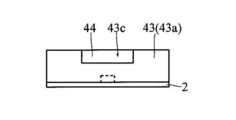
- the reflection member 43 of the fourth embodiment includes a wall portion 43a erected on the LED mounting surface 2a, and a side surface of the wall portion 43a is a light reflection surface 43b.
- the fourth embodiment when the light emitting device 40 is viewed from a direction parallel to the LED mounting surface 2a, a pair of light extraction openings facing in opposite directions to the wall 43a of the reflecting member 43.
- One set of 43c is formed.
- a pair of side end portions parallel to a predetermined direction of the LED mounting surface 2a is provided with a wall portion 43a of the reflection member 43 extending from one end of the side end portion to the entire area of the other end.
- the wall part 43a of the reflection member 43 is standingly arranged over the whole area also in a pair of edge
- the height of a part of the wall portion 43a of the reflecting member 43 standing on the pair of side end portions orthogonal to the predetermined direction of the LED mounting surface 2a is reduced, thereby the reflecting member 43.
- An opening for extracting light (a notched region) 43c is formed in the wall 43a (see FIG. 29).
- the LED mounting surface 2a is not divided into a plurality of parts.
- One LED 1 is mounted on the LED mounting surface 2 a that is not divided into a plurality, and the LED 1 is sealed with a sealing member 44. Therefore, in the fourth embodiment, one light emitting region has two light extraction openings (notched regions located on the side perpendicular to the predetermined direction of the LED mounting surface 2a) 43c.
- the planar shape of the light emitting region is an elongated hole shape.
- the same effects as in the first embodiment can be obtained by configuring as described above.
- light extracted in the front direction increases and light extracted in the horizontal direction decreases compared to the first embodiment.
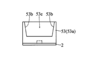
- the reflecting member 53 of the fifth embodiment includes a wall portion 53a erected on the LED mounting surface 2a, and the side surface of the wall portion 53a is a light reflecting surface 53b.
- a pair of light extraction openings 53c facing in opposite directions is formed in the wall 53a of the reflecting member 53 in the same manner as in the fourth embodiment.
- the wall 53a of the reflecting member 53 is erected over a whole area at a pair of side end portions parallel to a predetermined direction of the LED mounting surface 2a, and a pair of orthogonal to the predetermined direction of the LED mounting surface 2a.
- a wall 53a of the reflecting member 53 is also erected over the entire region at the side end.
- the light emitting device 50 is placed on the LED mounting surface 2a.
- the light extraction opening 53c is formed in the wall 53a of the reflecting member 53 (see FIG. 32).
- a part of the wall portion 53a of the reflecting member 53 crosses the center of the LED mounting surface 2a in a direction orthogonal to the predetermined direction, and is partitioned by that.
- One LED 1 is mounted on each of the two regions of the LED mounting surface 2a.
- the planar shape of the light emitting region is circular.
- a step is provided in the middle of the wall 53a of the reflecting member 53, and the thickness of the sealing member 54 is adjusted to the height of the step. That is, as in the third embodiment, a part of the light reflecting surface 53 b is exposed by making the thickness of the sealing member 54 smaller than the height of the wall portion 53 a of the reflecting member 53.
- the thickness of the sealing member 54 is made smaller than the height of the wall portion 53a of the reflecting member 53 to expose a part of the light reflecting surface 53b, so that the third Optical characteristics similar to those of the embodiment can be obtained. That is, as the optical characteristics of the light emitting device 50 of the fifth embodiment, the light extracted in the lateral direction further increases in the longitudinal direction, and is further condensed in the lateral direction.
- a step is provided in the middle of the wall portion 53a of the reflecting member 53, and the thickness of the sealing member 54 is adjusted to the height of the step. The occurrence of variations can be suppressed. At the same time, since the side surface of the sealing member 54 is not exposed, peeling of the sealing member 54 is less likely to occur, and reliability can be improved.
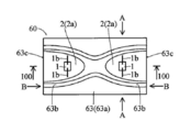
- the reflecting member 63 of the sixth embodiment includes a wall portion 63a standing on the LED mounting surface 2a, and the side surface of the wall portion 63a is a light reflecting surface 63b.
- the wall portion 63a of the reflecting member 63 stands on the entire pair of side end portions parallel to the predetermined direction (longitudinal direction) of the LED mounting surface 2a.
- the wall portion 63a of the reflecting member 63 is not provided upright at the pair of side end portions orthogonal to the predetermined direction of the LED mounting surface 2a. That is, when the light emitting device 60 is viewed from a direction parallel to the LED mounting surface 2a, a pair of light extraction openings (predetermined on the LED mounting surface 2a) facing the opposite directions to the wall 63a of the reflecting member 63.
- One set of opening regions 63c located on the side perpendicular to the direction is formed (see FIG. 35).
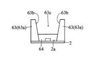
- the height of a part of wall part 63a of the reflection member 63 is smaller than the height of another part, and LED mounting surface 2a is based on a part of wall part 63a with the small height. Is divided into two regions. Then, one LED 1 is mounted on each of the two regions of the LED mounting surface 2a delimited by a part of the wall 63a of the reflecting member 63.
- the planar shape of the light emitting region (two regions of the LED mounting surface 2a divided by a part of the wall 63a of the reflecting member 63) is a semi-elliptical shape.
- the thickness of the sealing member 64 is set to a height of a wall portion 63a of the reflecting member 63 (a portion other than the portion dividing the LED mounting surface 2a into two regions) 63a. By making it smaller than this, a part of the light reflecting surface 63b is exposed.
- the LED mounting surface is reduced by reducing the height of a part of the wall 63a of the reflecting member 63 (the portion that divides the LED mounting surface 2a into two regions). It can suppress that the boundary of two area
- the thickness of the sealing member 64 is made smaller than the height of the wall portion 63a of the reflecting member 63 to expose a part of the light reflecting surface 63b, so that the third Optical characteristics similar to those of the embodiment can be obtained. That is, as the optical characteristics of the light emitting device 60 of the sixth embodiment, the light extracted in the lateral direction further increases in the longitudinal direction and is further condensed in the lateral direction.
- the light reflecting surface 63b composed only of the linearly inclined surface is not formed, but the linearly inclined surface and the curved surface are formed.
- a light reflecting surface 63b having a two-stage structure including a surface inclined to each other may be formed.
- the thickness of the sealing member 64 may be adjusted to the height of the step. If comprised in this way, it can suppress that the thickness of the sealing member 64 varies.
- the reflection member 73 of the seventh embodiment includes a wall portion 73a erected on the LED mounting surface 2a, and the side surface of the wall portion 73a is a light reflection surface 73b.
- the wall portion 73a of the reflecting member 73 stands on the entire pair of side end portions parallel to the predetermined direction (longitudinal direction) of the LED mounting surface 2a.
- a pair of side end portions orthogonal to the predetermined direction of the LED mounting surface 2a is provided with a region opened without the wall portion 73a of the reflecting member 73 standing. That is, when the light emitting device 70 is viewed from a direction parallel to the LED mounting surface 2a, a pair of light extraction openings (predetermined on the LED mounting surface 2a) facing the opposite directions to the wall 73a of the reflecting member 73.
- a pair of opening regions 73c located on the side perpendicular to the direction is formed (see FIG. 39).
- one light emitting region has two light extraction openings (opening regions located on the side perpendicular to the predetermined direction of the LED mounting surface 2a) 73c. Further, the planar shape of the light emitting region is such that a constriction is provided at the center of the rectangle.
- the reflecting member 83 of the eighth embodiment includes a wall portion 83a erected on the LED mounting surface 2a, and the side surface of the wall portion 83a is a light reflecting surface 83b.
- the wall portion 83a of the reflecting member 83 stands on the entire pair of side end portions parallel to the predetermined direction (longitudinal direction) of the LED mounting surface 2a.
- a pair of side end portions orthogonal to the predetermined direction of the LED mounting surface 2a is provided with a region opened without the wall 83a of the reflecting member 83 standing. That is, when the light emitting device 80 is viewed from a direction parallel to the LED mounting surface 2a, a pair of light extraction openings (predetermined on the LED mounting surface 2a) facing the opposite directions to the wall 83a of the reflecting member 83.
- One set of opening regions 83c located on the side perpendicular to the direction is formed (see FIG. 42).
- the LED mounting surface 2a is not divided into a plurality, and a plurality (three) of LEDs 1 are mounted on the LED mounting surface 2a that is not divided into a plurality. ing.
- the planar shape of the light emitting region is rectangular.
- a part of the light reflecting surface 83b is exposed by making the thickness of the sealing member 84 smaller than the height of the wall portion 83a of the reflecting member 83. Yes.
- a step is provided in the middle of the wall portion 83a of the reflecting member 83 in order to suppress variation in the thickness of the sealing member 84. You may make it match
- the LED 1 is mounted on a lead frame 92, and a reflecting member 93 is fixed to the lead frame 92.
- the LED 1 mounted on the lead frame 92 is sealed with a sealing member 94.
- the lead frame 92 is an example of the “base” in the present invention.
- the lead frame 92 of the ninth embodiment is formed so that the LED mounting surface (element mounting surface) 92a has a quadrangular shape.
- the lead frame 92 has frame portions 92b and 92c that are electrically insulated from each other and have different plane areas. Then, the LED 1 is fixed to the LED mounting surface 92a of the frame portion 92b having a larger plane area via the adhesive paste 1a. Further, one electrode of the LED 1 is electrically connected to the LED mounting surface 92a of the frame portion 92b through a wire 1b. Further, the other electrode of the LED 1 is electrically connected to the LED mounting surface 92a of the frame portion 92c having a smaller plane area via the wire 1b.
- the reflecting member 93 of the ninth embodiment includes a wall portion 93a erected on the LED mounting surface 92a.
- the side surface of the wall portion 93a of the reflecting member 93 is inclined obliquely, and the inclined side surface of the wall portion 93a of the reflecting member 93 is a light reflecting surface 93b.
- the wall 93a (light reflecting surface 93b) of the reflecting member 93 is formed in a frame shape having a circular inner periphery and a rectangular outer periphery.
- the reflection member 93 surrounds the LED 1 with its wall portion 93a (light reflection surface 93b) in a state where the reflection member 93 is bonded and fixed to the LED mounting surface 2a.
- the ninth embodiment when the light emitting device 90 is viewed from a direction parallel to the LED mounting surface 92a, a pair of light extraction openings facing in opposite directions to the wall portion 93a of the reflecting member 93.
- Two sets of 93c are formed. Specifically, when the light emitting device 90 is viewed from the A direction and the B direction, a part of the wall part 93a of the reflecting member 93 is notched, so that the height of a part of the wall part 93a of the reflecting member 93 is increased. Is smaller than the height of other parts. Then, an opening region (a notched region) generated thereby is an opening portion 93c for extracting light (see FIG. 46).
- the four portions of the frame portion 92b are convex portions 92d that protrude toward the reflecting member 93 rather than the other portions.
- four concave portions 93 d having a shape reflecting the shape of the convex portion 92 d of the lead frame 92 are formed in the wall portion 93 a of the reflecting member 93.
- the convex portion 92d of the lead frame 92 is press-fitted (inserted) into the concave portion 93d of the reflective member 93 so that the reflective member 93 directly contacts only the convex portion 92d of the lead frame 92. That is, in this state, only the frame portion 92 b is in direct contact with the reflecting member 93, and the frame portion 92 c is not in direct contact with the reflecting member 93. For this reason, even if the reflecting member 93 is made of metal, the frame portions 92 b and 92 c are not electrically connected to each other via the reflecting member 93. In FIG. 47, there is shown an interval between the convex portion 92d of the lead frame 92 and the concave portion 93d of the reflecting member 93, but this interval may be omitted.
- a translucent resin member 95 is embedded between the lead frame 92 and the reflection member 93, and the lead frame 92 and the reflection member 93 are bonded to each other by the resin member 95. . That is, the wall portion 93 a of the reflecting member 93 is erected on the LED mounting surface 92 a through the resin member 95.
- the resin member 95 is also embedded between the frame portion 92b and the frame portion 92c.
- the constituent material of the resin member 95 may be the same as the constituent material of the sealing member 94. In that case, the sealing step and the bonding step may be performed simultaneously.
- the lead frame 92 is used as a base on which the LED 1 is mounted, the same effects as those of the first and second embodiments can be obtained.
- the convex portion 92d is formed on the lead frame 92
- the concave portion 93d is formed on the reflective member 93
- the convex portion 92d of the lead frame 92 is formed on the concave portion 93d of the reflective member 93.
- only one pair of light extraction openings 93c facing in opposite directions is provided as in the first to third modifications shown in FIGS. It may be. If comprised in this way, in the direction where the opening part 93c for a pair of light extraction exists, light can be spread in a horizontal direction and directivity can be narrowed in the direction orthogonal to it.
- the shape of the LED mounting surface 92a exposed from the reflecting member 93 may be an elliptical shape as in the first modification shown in FIG.
- the shape of the LED mounting surface 92a exposed from the reflecting member 93 may be a bowl shape, and a plurality of LEDs 1 may be mounted there. .
- the LED mounting surface 92a may be divided into two regions by the reflecting member 93, and the LEDs 1 may be mounted one by one in the two regions.
- the lead frame 102 has a square LED mounting surface 102a and is divided into two frame portions 102b and 102c. Is used.
- the wall part 103a which consists of a resin molding part is standingly arranged in the LED mounting surface 102a, and the wall part 103a is used as the reflection member 103.
- the wall portion 103a of the reflecting member 103 is erected over the entire region at the pair of side end portions parallel to the predetermined direction of the LED mounting surface 102a.
- a pair of side end portions orthogonal to the direction is provided with a region where the wall portion 103a of the reflecting member 103 is opened without being erected. That is, when the light emitting device 110 is viewed from a direction parallel to the LED mounting surface 102a, a pair of light extraction openings (predetermined on the LED mounting surface 102a) facing the opposite directions to each other on the wall portion 103a of the reflecting member 103.
- a pair of opening regions 103c located on the side perpendicular to the direction is formed.
- a part of the wall portion 103a of the reflecting member 103 crosses the center of the LED mounting surface 102a in a direction orthogonal to the predetermined direction, thereby dividing the LED mounting surface 102a into two regions. ing.
- One LED 1 is mounted on each of the two regions of the LED mounting surface 102 a separated by a part of the wall 103 a of the reflecting member 103, and the LED 1 is sealed with the sealing member 104.
- a predetermined portion of the lead frame 102 may protrude from the LED mounting surface 102a, and the protruding portion may be used as the reflecting member 103 (wall portion 103a). . If comprised in this way, since the light reflection surface 103b will be metal, it can suppress that inconveniences, such as discoloration of the light reflection surface 103b, arise. In this case, if the resin molding portion 105 is embedded behind the portion protruding from the LED mounting surface 102a, the mechanical strength of the lead frame 102 is improved while the frame portions 102b and 102c are fixed to each other. Can do.
Landscapes
- Led Device Packages (AREA)
Abstract
【課題】輝度ムラの発生を抑制することが可能な発光装置を提供する。 【解決手段】この発光装置10は、LED1と、LED1が搭載されるLED搭載面2aを有する配線基板2と、LED搭載面2aに立設された壁部3aからなり、その壁部3aの側面が光反射面3bとなる反射部材3とを備えている。そして、LED搭載面2aに対して平行な方向から見た場合に、互いに逆方向に向く一対の光取り出し用の開口部3cが反射部材3の壁部3aに1組以上形成された状態となっている。
Description
本発明は、発光装置および発光装置モジュールに関する。
従来、発光ダイオード素子(LED)などの発光素子を備えた発光装置が知られている(たとえば、特許文献1参照)。以下に、従来の発光装置の構成を簡単に説明する。
従来の発光装置では、LEDが基板に搭載され、その状態でLEDが封止部材によって封止されている。そして、従来では、LEDからの光に指向性を持たせるために、枠状の光反射面を有する反射部材を基板の搭載面に取り付け、その反射部材の光反射面によってLEDの周囲を完全に取り囲んでいる。
しかしながら、上記した従来の発光装置では、それを複数用いて照明装置(液晶表示装置用バックライトや蛍光灯など)を作製した場合、それぞれの発光装置の発光が独立して見えることでギラツキ感(グレア)が発生してしまう。具体的に言うと、隣り合う発光装置の間の領域が暗くなるため、全体的に見て輝度ムラが発生した状態となってしまう。なお、この問題を解消する方法として、たとえば、光拡散部材によって光を拡散するという方法が考えられる。ただし、光拡散部材を用いた場合には、光の利用効率が低下してしまうという新たな問題が発生する。
本発明は、上記のような課題を解決するためになされたものであり、輝度ムラの発生を抑制することが可能な発光装置および発光装置モジュールを提供することを目的とする。
上記の目的を達成するために、本発明の第1の局面による発光装置は、光を生成する発光素子と、発光素子が搭載される素子搭載面を有する基台と、素子搭載面に立設された壁部からなり、その壁部の側面が光反射面となる反射部材とを備えている。そして、素子搭載面に対して平行な方向から見た場合に、互いに逆方向に向く一対の光取り出し用の開口部が反射部材の壁部に1組以上形成された状態となっている。
なお、以下の説明では、素子搭載面に対して垂直な方向(反射部材の壁部の立設方向)およびその近傍の方向を単に正面方向と言うとともに、素子搭載面に対して平行な方向(反射部材の壁部の立設方向と直交する方向)およびその近傍の方向を単に横方向と言う。
この第1の局面による発光装置では、上記のように、素子搭載面に対して平行な方向から見た場合に、互いに逆方向に向く一対の光取り出し用の開口部が反射部材の壁部に1組以上形成された状態となるように構成することによって、発光装置から放出される光のうち、反射部材の壁部で反射されて正面方向に取り出される光については減少するが、光取り出し用の開口部を介して横方向に取り出される光が新たに発生する。
これにより、第1の局面による発光装置を複数準備し、その複数の発光装置を直線状に配列することで線状光源(発光装置モジュール)を作製する場合に、複数の発光装置のそれぞれに互いに逆方向に向く一対の光取り出し用の開口部を1組だけ形成するとともに、それぞれの光取り出し用の開口部が互いに向き合うように複数の発光装置を配置すれば、隣り合う発光装置の間の領域が暗くなってしまうのを抑制することができる。すなわち、線状光源の長手方向(発光装置の配列方向)における輝度ムラの発生を抑制することが可能となる。ところで、このような線状光源の用途としては、エッジライト型の液晶表示装置用バックライト、蛍光灯およびスキャナー用光源などが考えられる。
なお、第1の局面による発光装置を複数用いた面状光源(たとえば、直下型の液晶表示装置用バックライト)を作製する場合には、複数の発光装置のそれぞれに互いに逆方向に向く一対の光取り出し用の開口部を2組形成し、それぞれの光取り出し用の開口部が互いに向き合うように複数の発光装置をマトリクス状に配置すれば、輝度ムラの発生を抑制することが可能となる。
上記第1の局面による発光装置において、素子搭載面に対して平行な方向から見た場合に、反射部材の壁部が立設されていない領域、および、反射部材の壁部が凹状に切り欠かれた領域のうちの少なくとも一方の領域が設けられた状態となっており、反射部材の壁部が立設されていない領域、および、反射部材の壁部が凹状に切り欠かれた領域のうちの少なくとも一方の領域が光取り出し用の開口部とされていることが好ましい。このように構成すれば、容易に、光を横方向に取り出すための光取り出し用の開口部を得ることができる。
上記第1の局面による発光装置において、発光素子を封止するための封止部材をさらに備え、その封止部材が光取り出し用の開口部から露出されていることが好ましい。このように構成すれば、容易に、光取り出し用の開口部を介して、封止部材で封止された発光素子からの光を横方向に取り出すことができる。
上記第1の局面による発光装置において、素子搭載面が互いに平行な一対の辺を2組有する四角形状に形成されており、素子搭載面の2組の一対の辺のうち、少なくとも1組の一対の辺側のそれぞれに光取り出し用の開口部が配置されていることが好ましい。このように構成すれば、たとえば、素子搭載面の所定方向に平行な一対の辺側のそれぞれには光取り出し用の開口部を配置せず、素子搭載面の所定方向と直交する一対の辺側のそれぞれにのみ光取り出し用の開口部を配置すれば、所定方向と直交する方向における指向性を狭く保持したまま、所定方向における指向性を広げることができる。さらに、素子搭載面の全ての辺側のそれぞれに光取り出し用の開口部を配置すれば、所定方向およびその方向と直交する方向の両方向における指向性を広げることができる。
上記第1の局面による発光装置において、素子搭載面が反射部材の壁部の一部によって2つ以上の領域に区切られていてもよい。また、この場合には、素子搭載面の2つ以上の領域のそれぞれに発光素子が搭載されていることが好ましい。このように構成すれば、光取り出し用の開口部に向かって反射される光が多くなるので、光取り出し用の開口部を介して横方向に取り出される光をより増大させることができる。
また、素子搭載面が反射部材の壁部の一部によって2つ以上の領域に区切られた構成において、素子搭載面を2つ以上に区切っている反射部材の壁部の一部の高さが、反射部材の壁部の他の部分の高さよりも小さくなっていてもよい。このように構成すれば、素子搭載面を反射部材の壁部の一部によって2つ以上の領域に区切ったとしても、素子搭載面の2つ以上の領域の境界が暗くなるのを抑制することができる。
さらに、素子搭載面が反射部材の壁部の一部によって2つ以上の領域に区切られた構成において、素子搭載面を2つ以上に区切っている反射部材の壁部の一部に、壁厚方向に貫通する貫通穴が形成されていてもよい。このように構成すれば、発光素子を封止部材で封止する場合、反射部材の貫通穴にも封止部材を埋め込むことにより、封止部材が反射部材の貫通穴に係合した状態になる。これにより、封止部材の剥離を抑制することができ、信頼性の向上を図ることが可能となる。
上記第1の局面による発光装置において、発光素子が発光ダイオード素子であることが好ましい。
また、本発明の第2の局面による発光装置モジュールは、上記第1の局面による発光装置を複数備えている。このように構成すれば、容易に、輝度ムラの発生を抑制することができる。
上記第2の局面による発光装置モジュールにおいて、複数の発光装置のそれぞれの光取り出し用の開口部が互いに向き合わされていることが好ましい。このように構成すれば、隣り合う発光装置の間の領域が暗くなるのが抑制され、輝度ムラの発生をより抑制することができる。
上記第2の局面による発光装置モジュールにおいて、複数の発光装置が直線的に配列されていてもよい。このように構成すれば、輝度ムラの発生が抑制された線状光源を容易に得ることができる。
以上のように、本発明によれば、容易に、輝度ムラの発生を抑制することができる。
(第1実施形態)
以下に、図1~図4を参照して、第1実施形態による発光装置10の構成について詳細に説明する。
以下に、図1~図4を参照して、第1実施形態による発光装置10の構成について詳細に説明する。
第1実施形態の発光装置10は、図1~図4に示すように、光を生成するLED1、そのLED1が搭載される配線基板2、LED1で生成された光を反射するための反射部材3、および、LED1を封止するための封止部材4などを備えている。なお、LED1は本発明の「発光素子」の一例であり、配線基板2は本発明の「基台」の一例である。
LED1が搭載される配線基板2はガラスエポキシ基板であって、そのLED搭載面(素子搭載面)2aが四角形状となるように形成されている。そして、LED搭載面2aへのLED1の搭載は、接着用ペースト1aを介して行われている。また、配線基板2には電極パターン(図示せず)が設けられており、LED1の電極がワイヤ1bを介して電気的に接続されている。
反射部材3は樹脂や金属などを構成材料としているとともに、LED搭載面2aに接着固定されている。さらに、反射部材3は、LED搭載面2aに接着固定された状態において、LED搭載面2aから壁状に突出するような形状に形成されている。すなわち、反射部材3は、LED搭載面2aに立設された壁部3aからなっていることになる。そして、反射部材3の壁部3aの側面はLED搭載面2aに対して斜めに傾斜しており、その反射部材3の壁部3aの傾斜した側面が光反射面3bとなっている。
ここで、第1実施形態では、発光装置10をLED搭載面2aに対して平行な方向から見た場合、反射部材3の壁部3aに、互いに逆方向に向く一対の光取り出し用の開口部3cが1組形成された状態となっている。具体的に言うと、LED搭載面2aの面内のうちで、所定方向に平行な一対の辺側端部には、その辺側端部の一端から他端の全域にわたって反射部材3の壁部3aが立設されているが、所定方向と直交する一対の辺側端部には、反射部材3の壁部3aが立設されずに開口された領域(光取り出し用の開口部3c)が設けられている。すなわち、発光装置10をA方向から見ると、反射部材3の壁部3aによって光の進路が完全に遮られた状態となっている(図3参照)。その一方、発光装置10をB方向から見ると、両端部側にのみ反射部材3の壁部3aが立設され、中央部側に光取り出し用の開口部3cが設けられた状態となっている(図4参照)。
また、第1実施形態では、反射部材3の壁部3aの一部がLED搭載面2aの中央を所定方向と直交する方向に横切っており、それによってLED搭載面2aが2つの領域に区切られている。そして、反射部材3の壁部3aの一部によって区切られたLED搭載面2aの2つの領域にLED1が1つずつ搭載されている。したがって、第1実施形態では、2つの発光領域が光取り出し用の開口部(LED搭載面2aの所定方向と直交する辺側に位置する開口領域)3cを1つずつ持っていることになる。なお、第1実施形態では、発光領域の平面形状が半円形状であって、その直線状の辺側に光取り出し用の開口部3cが配置されている。
また、第1実施形態では、LED1が封止部材4によって封止されているが、その封止部材4は、光取り出し用の開口部3cから露出されている。
第1実施形態では、上記のように、発光装置10を素子搭載面2aに対して平行な方向から見た場合に、互いに逆方向に向く一対の光取り出し用の開口部3cが反射部材3の壁部3aに1組形成された状態となるように構成することによって、発光装置10から放出される光のうち、反射部材3の壁部3aで反射されて正面方向に取り出される光については減少するが、光取り出し用の開口部3cを介して横方向に取り出される光が新たに発生する。
このため、たとえば、図5に示すように、第1実施形態の発光装置10を複数準備し、その複数の発光装置10を実装基板5に直線状に実装することで発光装置モジュール(線状光源)11を作製する場合、それぞれの光取り出し用の開口部3cが互いに向き合うように複数の発光装置10を配置することにより、隣り合う発光装置10の間の領域が暗くなるのを抑制することができる。したがって、この発光装置モジュール11を蛍光灯12(図6参照)の光源として用いれば、図7に示すように、X方向(長手方向)において輝度ムラの発生を従来よりも抑制することができる。また、図8に示すように、Y方向(短手方向)においては指向性が狭めとなる。なお、Y方向(短手方向)における指向性については、従来と比べてほとんど違いはない。
また、第1実施形態では、上記のように、反射部材3の壁部3aが立設されていない領域を光取り出し用の開口部3cとすることによって、容易に、光を横方向に取り出すための光取り出し用の開口部3cを得ることができる。
また、第1実施形態では、上記のように、封止部材4を光取り出し用の開口部3cから露出させることによって、容易に、光取り出し用の開口部3cを介して、封止部材4で封止されたLED1からの光を横方向に取り出すことができる。
また、第1実施形態では、上記のように、反射部材3の壁部3aの一部でLED搭載面2aを2つの領域に区切り、そのLED搭載面2aの2つの領域にLED1を1つずつ搭載することによって、光取り出し用の開口部3cを介して横方向に取り出される光をより増大させることができる。
また、第1実施形態では、上記のように、LED搭載面2aの所定方向と直交する一対の辺側端部にのみ光取り出し用の開口部3cを設け、LED搭載面2aの所定方向に平行な一対の辺側端部については全域にわたって反射部材3の壁部3aを立設することによって、発光装置10の外形が堅牢に保持されるため、ピックアップなどのハンドリングを容易に行うことができる。
ところで、第1実施形態の発光装置10は、たとえば、以下のようにして製造することができる。
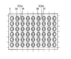
すなわち、図9に示すように、まず、マトリクス状に配列された円形状の貫通穴3dを複数有する反射部材3を準備する。なお、反射部材3の貫通穴3dは、その内側面が光反射面となるものである。
次に、大判の配線基板2を準備するとともに、その大判の配線基板2のLED搭載面2aに反射部材3を接着固定する。そして、LED搭載面2aに対してチップボンディングおよびワイヤボンディングを行った後、樹脂封止する。これにより、複数の発光装置10がマトリクス状に一体的に連結された構造体が得られる。
最後に、反射部材3の円形状の貫通穴3dが半円形状となるように、図中の破線に沿ってダイシングを行う。これにより、図10に示すように、複数の発光装置10が個片に分離され、第1実施形態の発光装置10が製造される。
なお、上記した第1実施形態の構成において、図11に示す第1変形例のように、反射部材3の壁部3aの高さをより大きくしてもよい。このように構成すれば、光取り出し用の開口部3cを介して横方向に取り出される光がさらに増大する。
また、上記した第1実施形態の構成において、図12~図14に示す第2変形例のように、光反射面3bを直線的に傾斜させるのではなく、曲線的に傾斜させてもよい。
さらに、配線基板2に対する反射部材3の取り付け方法についても変更可能である。なお、第1実施形態の第2変形例では、以下のような取り付け方法を採用している。
すなわち、この第1実施形態の第2変形例では、配線基板2の反射部材3と重畳する部分内に穴部2bを形成し、その配線基板2の穴部2bに挿入可能な取付片3eを反射部材3に形成している。そして、反射部材3の取付片3eの先端を配線基板2の穴部2bから裏面(LED搭載面2aとは反対側の面)側に突出させ、その反射部材3の取付片3eの先端を潰すことによって、配線基板2への反射部材3の取り付けを行っている。このような取り付け方法を採用すれば、容易に、配線基板2に対する反射部材3の取り付けを強固にすることができる。
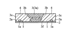
また、上記した第1実施形態の構成において、図15および図16に示す第3変形例のように、反射部材3の壁部3aの断面形状を台形状にするのではなく、逆台形状としてもよい。このように構成すれば、封止部材4が剥離しにくくなり、信頼性の向上を図ることができる。
さらに、この場合、反射部材3の壁部3aの一部(LED搭載面2aを2つの領域に区切っている部分)に貫通穴3fを形成するとともに、その貫通穴3fにも封止部材4を埋め込むようにすれば、封止部材4が反射部材3の貫通穴3fに係合した状態となるので、封止部材4の剥離をより抑制することができる。
また、上記した第1実施形態の構成において、図17および図18に示す第4および第5変形例のように、LED搭載面2aを反射部材3によって3つ以上に区切るとともに、反射部材3によって区切られたLED搭載面2aの3つ以上の領域にLED1を1つ以上ずつ搭載するようにしてもよい。
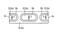
具体的に言うと、図17(第4変形例)には、LED搭載面2aを反射部材3によって4つに区切ることで4つの発光領域を設け、その4つの発光領域を直線状に配列したものが図示されている。そして、両端の発光領域はLED1を1つずつ含んでいるとともに、それ以外の発光領域はLED1を2つずつ含んでいる。さらに、両端の発光領域は光取り出し用の開口部3cを持っているとともに、それ以外の発光領域は反射部材3によって完全に取り囲まれている。また、両端の発光領域の平面形状は半円形状となっており、それ以外の発光領域は円形状となっている。なお、両端に位置する発光領域の平面形状は、それ以外の発光領域を半分に切った形状に相当する。
また、図18(第5変形例)には、LED搭載面2aを反射部材3によって3つに区切ることで3つの発光領域を設け、その3つの発光領域を直線状に配列したものが図示されている。そして、その3つの発光領域はLED1を1つずつ含んでいる。また、両端の発光領域は光取り出し用の開口部3cを持っているとともに、それ以外の発光領域は反射部材3によって完全に取り囲まれている。また、両端の発光領域の平面形状は長穴を半分に切った形状となっており、それ以外の発光領域は長穴形状となっている。なお、両端に位置する発光領域の平面形状は、それ以外の発光領域を半分に切った形状に相当する。
(第2実施形態)
以下に、図19~図21を参照して、第2実施形態による発光装置20の構成について説明する。
以下に、図19~図21を参照して、第2実施形態による発光装置20の構成について説明する。
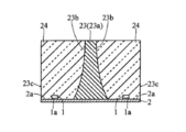
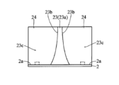
第2実施形態では、図19~図21に示すような反射部材23が用いられている。この第2実施形態の反射部材23は、LED搭載面2aに立設された壁部23aからなっている。さらに、反射部材23の壁部23aの側面はLED搭載面2aに対して斜めに傾斜しており、その反射部材23の壁部23aの傾斜した側面が光反射面23bとなっている。
ここで、第2実施形態では、発光装置20をLED搭載面2aに対して平行な方向から見た場合、反射部材23の壁部23aに、互いに逆方向に向く一対の光取り出し用の開口部23cが2組形成された状態となっている。具体的に言うと、反射部材23の壁部23aは、LED搭載面2aの中央を所定方向に横切り、かつ、LED搭載面2aの中央を所定方向と直交する方向に横切るように立設されている。そして、LED搭載面2aの4つの角部には、反射部材23の壁部23aが立設されずに開口された領域(光取り出し用の開口部23c)が設けられている。すなわち、発光装置20をA方向およびB方向から見ると、中央部側にのみ反射部材23の壁部23aが立設され、両端部側に光取り出し用の開口部23cが設けられた状態となっている(図21参照)。
また、この構成の場合、反射部材23によってLED搭載面2aが4つの領域に区切られていることになる。そして、反射部材23によって区切られたLED搭載面2aの4つの領域にLED1が1つずつ搭載されており、そのLED1が封止部材24で封止されている。したがって、第2実施形態では、4つの発光領域が光取り出し用の開口部(LED搭載面2aの角側に位置する開口領域)23cを1つずつ持っていることになる。なお、第2実施形態では、発光領域の平面形状が扇形状(円形を4等分した形状)であって、その直線状の辺側に光取り出し用の開口部23cが配置されている。
第2実施形態では、上記のように構成することによって、第1実施形態と同様の効果を得ることができるが、その指向性はより広くなる。
これにより、たとえば、第2実施形態の発光装置20を複数準備し、その複数の発光装置20をマトリクス状に配置することで発光装置モジュールを作製すれば、直下型の液晶表示装置用バックライトとして好適な面状光源を得ることができる。
なお、上記した第2実施形態の構成において、図22および図23に示すように、反射部材23の壁部23aをオーバーハング形状とし、その反射部材23のオーバーハング部23dでLED1を覆うようにしてもよい。このように構成すれば、正面方向への光の広がりが抑制され、その分、横方向への光の広がりがより大きくなる。したがって、この変形例による発光装置を複数用いて面状光源(直下型の液晶表示装置用バックライト)を作製すれば、輝度ムラの発生のさらなる低減を図ることが可能となる。
また、上記した第2実施形態の構成において、白色LED(たとえば、青色LEDと蛍光体とを組み合わせたもの)を4つの発光領域に1つ以上ずつ配置してもよいが、白色LEDを用いなくてもよい。すなわち、赤色LED、緑色LEDおよび青色LEDを個々に準備し、それらの発光を混色して白色光を得るようにしてもよい。
ところで、赤色LED、緑色LEDおよび青色LEDを用いる場合には、赤色LED、緑色LEDおよび青色LEDを同数ずつ含むLED群を4つの発光領域のそれぞれに配置してもよいが、光量バランスを考慮して、LED群に含まれる緑色LEDの数を他のLEDの数よりも多くしてもよい。具体的に言うと、1つの赤色LEDと、2つの緑色LEDと、1つの青色LEDとを含むものをLED群としてもよい。また、光量バランスを調整する別の方法として、4つの発光領域のそれぞれに、赤色LED、緑色LED、緑色LEDおよび青色LEDを別個に配置してもよい。
(第3実施形態)
以下に、図24~図26を参照して、第3実施形態による発光装置30の構成について説明する。
以下に、図24~図26を参照して、第3実施形態による発光装置30の構成について説明する。
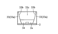
第3実施形態では、図24~図26に示すような反射部材33が用いられている。具体的な構造としては、第3実施形態の反射部材33は、LED搭載面2aに立設された壁部33aからなっているとともに、その壁部33aの側面を光反射面33bとしている。
ここで、第3実施形態では、上記第1実施形態と同様、LED搭載面2aの所定方向(長手方向)に平行な一対の辺側端部には全域にわたって反射部材33の壁部33aが立設されているが、LED搭載面2aの所定方向と直交する一対の辺側端部には反射部材33の壁部33aが立設されずに開口された領域が設けられている。すなわち、発光装置30をLED搭載面2aに対して平行な方向から見た場合、反射部材33の壁部33aに、互いに逆方向に向く一対の光取り出し用の開口部(LED搭載面2aの所定方向と直交する
辺側に位置する開口領域)33cが1組形成された状態となっている(図26参照)。なお、図示しないが、発光装置30をA方向から見た場合には、反射部材33の壁部33aによって光の進路が完全に遮られた状態となっている。
辺側に位置する開口領域)33cが1組形成された状態となっている(図26参照)。なお、図示しないが、発光装置30をA方向から見た場合には、反射部材33の壁部33aによって光の進路が完全に遮られた状態となっている。
また、第3実施形態では、上記第1実施形態と同様、反射部材33の壁部33aの一部がLED搭載面2aの中央を所定方向と直交する方向に横切っており、それによって区切られたLED搭載面2aの2つの領域にLED1が1つずつ搭載されている。ただし、第3実施形態では、発光領域(反射部材33の壁部33aの一部によって区切られたLED搭載面2aの2つの領域)の平面形状が半楕円形状となっている。
さらに、第3実施形態では、封止部材34の厚みを反射部材33の壁部33aの高さよりも小さくすることで、光反射面33bの一部を露出させている。
第3実施形態では、上記のように構成することによって、第1実施形態と同様の効果を得ることができる。
また、第3実施形態では、上記のように、封止部材34の厚みを反射部材33の壁部33aの高さよりも小さくすることで光反射面33bの一部を露出させることによって、封止部材34の外部においても光の反射が行われる。このため、第3実施形態の発光装置30の光特性としては、その長手方向においては横方向に取り出される光がさらに増大し、短手方向においてはさらに集光されたものとなる。
(第4実施形態)
以下に、図27~図29を参照して、第4実施形態による発光装置40の構成について説明する。
以下に、図27~図29を参照して、第4実施形態による発光装置40の構成について説明する。
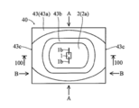
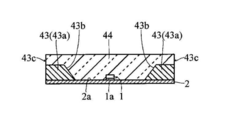
第4実施形態では、図27~図29に示すような反射部材43が用いられている。具体的な構造としては、第4実施形態の反射部材43は、LED搭載面2aに立設された壁部43aからなっているとともに、その壁部43aの側面を光反射面43bとしている。
ここで、第4実施形態では、発光装置40をLED搭載面2aに対して平行な方向から見た場合、反射部材43の壁部43aに、互いに逆方向に向く一対の光取り出し用の開口部43cが1組形成された状態となっている。具体的に言うと、LED搭載面2aの所定方向に平行な一対の辺側端部には、その辺側端部の一端から他端の全域にわたって反射部材43の壁部43aが立設されている。また、LED搭載面2aの所定方向と直交する一対の辺側端部にも全域にわたって反射部材43の壁部43aが立設されているが、その一部が凹状に切り欠かれている。すなわち、第4実施形態では、LED搭載面2aの所定方向と直交する一対の辺側端部に立設する反射部材43の壁部43aの一部の高さを小さくし、それによって反射部材43の壁部43aに光取り出し用の開口部(切り欠かれた領域)43cが形成された状態にしている(図29参照)。なお、図示しないが、発光装置40をA方向から見た場合には、反射部材43の壁部43aによって光の進路が完全に遮られた状態となっている。
さらに、第4実施形態では、上記した他の実施形態とは異なり、LED搭載面2aを複数に区切ってはいない。そして、複数に区切っていないLED搭載面2aに1つのLED1を搭載し、そのLED1を封止部材44で封止している。したがって、第4実施形態では、1つの発光領域が光取り出し用の開口部(LED搭載面2aの所定方向と直交する辺側に位置する切り欠き領域)43cを2つ持っていることになる。なお、第4実施形態では、発光領域の平面形状が長穴形状となっている。
第4実施形態では、上記のように構成することによって、第1実施形態と同様の効果を得ることができる。ただし、第4実施形態では、第1実施形態に比べて、正面方向に取り出される光が増大し、横方向に取り出される光が減少する。
(第5実施形態)
以下に、図30~図32を参照して、第5実施形態による発光装置50の構成について説明する。
以下に、図30~図32を参照して、第5実施形態による発光装置50の構成について説明する。
第5実施形態では、図30~図32に示すような反射部材53が用いられている。具体的な構造としては、第5実施形態の反射部材53は、LED搭載面2aに立設された壁部53aからなっているとともに、その壁部53aの側面を光反射面53bとしている。
ここで、第5実施形態では、上記第4実施形態と同様の方法により、互いに逆方向に向く一対の光取り出し用の開口部53cを反射部材53の壁部53aに1組形成している。具体的に言うと、LED搭載面2aの所定方向に平行な一対の辺側端部に全域にわたって反射部材53の壁部53aを立設するとともに、LED搭載面2aの所定方向と直交する一対の辺側端部にも全域にわたって反射部材53の壁部53aを立設している。そして、LED搭載面2aの所定方向と直交する一対の辺側端部に立設する反射部材53の壁部53aの一部の高さを小さくすることで、発光装置50をLED搭載面2aに対して平行な方向から見た場合に、反射部材53の壁部53aに光取り出し用の開口部53cが形成された状態となるようにしている(図32参照)。なお、図示しないが、発光装置50をA方向から見た場合には、反射部材53の壁部53aによって光の進路が完全に遮られた状態となっている。
また、第5実施形態では、上記第1実施形態と同様、反射部材53の壁部53aの一部がLED搭載面2aの中央を所定方向と直交する方向に横切っており、それによって区切られたLED搭載面2aの2つの領域にLED1が1つずつ搭載されている。ただし、第5実施形態では、発光領域(反射部材53の壁部53aの一部によって区切られたLED搭載面2aの2つの領域)の平面形状が円形状となっている。
さらに、第5実施形態では、反射部材53の壁部53aの途中に段差を設け、その段差の高さ位置に封止部材54の厚みを合わせている。すなわち、上記第3実施形態と同様、封止部材54の厚みを反射部材53の壁部53aの高さよりも小さくすることで、光反射面53bの一部を露出させている。
第5実施形態では、上記のように構成することによって、第1実施形態と同様の効果を得ることができる。
また、第5実施形態では、上記のように、封止部材54の厚みを反射部材53の壁部53aの高さよりも小さくすることで光反射面53bの一部を露出させることによって、第3実施形態と同様の光特性が得られる。すなわち、第5実施形態の発光装置50の光特性としては、その長手方向においては横方向に取り出される光がさらに増大し、短手方向においてはさらに集光されたものとなる。
なお、第5実施形態では、反射部材53の壁部53aの途中に段差を設け、その段差の高さ位置に封止部材54の厚みを合わせるようにしているので、封止部材54の厚みにバラツキが生じるのを抑制することができる。また、同時に、封止部材54の側面が露出しない構造となるため、封止部材54の剥離などが発生し難くなり、信頼性を向上させることができる。
(第6実施形態)
以下に、図33~図35を参照して、第6実施形態による発光装置60の構成について説明する。
以下に、図33~図35を参照して、第6実施形態による発光装置60の構成について説明する。
第6実施形態では、図33~図35に示すような反射部材63が用いられている。具体的な構造としては、第6実施形態の反射部材63は、LED搭載面2aに立設された壁部63aからなっているとともに、その壁部63aの側面を光反射面63bとしている。
ここで、第6実施形態では、上記第1実施形態と同様、LED搭載面2aの所定方向(長手方向)に平行な一対の辺側端部には全域にわたって反射部材63の壁部63aが立設されているが、LED搭載面2aの所定方向と直交する一対の辺側端部には反射部材63の壁部63aが立設されずに開口された領域が設けられている。すなわち、発光装置60をLED搭載面2aに対して平行な方向から見た場合、反射部材63の壁部63aに、互いに逆方向に向く一対の光取り出し用の開口部(LED搭載面2aの所定方向と直交する辺側に位置する開口領域)63cが1組形成された状態となっている(図35参照)。なお、図示しないが、発光装置60をA方向から見た場合には、反射部材63の壁部63aによって光の進路が完全に遮られた状態となっている。
さらに、第6実施形態では、反射部材63の壁部63aの一部の高さが他の部分の高さよりも小さくなっており、その高さが小さい壁部63aの一部によってLED搭載面2aが2つの領域に区切られている。そして、反射部材63の壁部63aの一部によって区切られたLED搭載面2aの2つの領域にLED1が1つずつ搭載されている。なお、第6実施形態では、発光領域(反射部材63の壁部63aの一部によって区切られたLED搭載面2aの2つの領域)の平面形状が半楕円形状となっている。
また、第6実施形態では、上記第3実施形態と同様、封止部材64の厚みを反射部材63の壁部(LED搭載面2aを2つの領域に区切っている部分以外の部分)63aの高さよりも小さくすることで、光反射面63bの一部を露出させている。
第6実施形態では、上記のように構成することによって、第1実施形態と同様の効果を得ることができる。
また、第6実施形態では、上記のように、反射部材63の壁部63aの一部(LED搭載面2aを2つの領域に区切っている部分)の高さを小さくすることによって、LED搭載面2aの2つの領域の境界が暗くなるのを抑制することができる。ただし、横方向に取り出される光は若干減少する。
また、第6実施形態では、上記のように、封止部材64の厚みを反射部材63の壁部63aの高さよりも小さくすることで光反射面63bの一部を露出させることによって、第3実施形態と同様の光特性が得られる。すなわち、第6実施形態の発光装置60の光特性としては、その長手方向においては横方向に取り出される光がさらに増大し、短手方向においてはさらに集光されたものとなる。
なお、上記した第6実施形態の構成において、図36に示すように、直線的に傾斜させた面のみからなる光反射面63bを形成するのではなく、直線的に傾斜させた面と曲線的に傾斜させた面とを含む2段構造の光反射面63bを形成するようにしてもよい。
また、この場合には、反射部材63の壁部63aの途中に段差が設けられるので、その段差の高さ位置に封止部材64の厚みを合わせるようにしてもよい。このように構成すれば、封止部材64の厚みにバラツキが生じるのを抑制することができる。
(第7実施形態)
以下に、図37~図39を参照して、第7実施形態による発光装置70の構成について説明する。
以下に、図37~図39を参照して、第7実施形態による発光装置70の構成について説明する。
第7実施形態では、図37~図39に示すような反射部材73が用いられている。具体的な構造としては、第7実施形態の反射部材73は、LED搭載面2aに立設された壁部73aからなっているとともに、その壁部73aの側面を光反射面73bとしている。
ここで、第7実施形態では、上記第1実施形態と同様、LED搭載面2aの所定方向(長手方向)に平行な一対の辺側端部には全域にわたって反射部材73の壁部73aが立設されているが、LED搭載面2aの所定方向と直交する一対の辺側端部には反射部材73の壁部73aが立設されずに開口された領域が設けられている。すなわち、発光装置70をLED搭載面2aに対して平行な方向から見た場合、反射部材73の壁部73aに、互いに逆方向に向く一対の光取り出し用の開口部(LED搭載面2aの所定方向と直交する辺側に位置する開口領域)73cが1組形成された状態となっている(図39参照)。なお、図示しないが、発光装置70をA方向から見た場合には、反射部材73の壁部73aによって光の進路が完全に遮られた状態となっている。
ところで、第7実施形態では、上記した他の実施形態とは異なり、複数に区切っていないLED搭載面2aに複数(2つ)のLED1を搭載し、そのLED1を封止部材74で封止している。したがって、第7実施形態では、1つの発光領域が光取り出し用の開口部(LED搭載面2aの所定方向と直交する辺側に位置する開口領域)73cを2つ持っていることになる。また、その発光領域の平面形状は、長方形の中央部にくびれを設けたような形状となっている。
(第8実施形態)
以下に、図40~図42を参照して、第8実施形態による発光装置80の構成について説明する。
以下に、図40~図42を参照して、第8実施形態による発光装置80の構成について説明する。
第8実施形態では、図40~図42に示すような反射部材83が用いられている。具体的な構造としては、第8実施形態の反射部材83は、LED搭載面2aに立設された壁部83aからなっているとともに、その壁部83aの側面を光反射面83bとしている。
ここで、第8実施形態では、上記第1実施形態と同様、LED搭載面2aの所定方向(長手方向)に平行な一対の辺側端部には全域にわたって反射部材83の壁部83aが立設されているが、LED搭載面2aの所定方向と直交する一対の辺側端部には反射部材83の壁部83aが立設されずに開口された領域が設けられている。すなわち、発光装置80をLED搭載面2aに対して平行な方向から見た場合、反射部材83の壁部83aに、互いに逆方向に向く一対の光取り出し用の開口部(LED搭載面2aの所定方向と直交する辺側に位置する開口領域)83cが1組形成された状態となっている(図42参照)。なお、図示しないが、発光装置80をA方向から見た場合には、反射部材83の壁部83aによって光の進路が完全に遮られた状態となっている。
また、第8実施形態では、上記第7実施形態と同様、LED搭載面2aを複数には区切ってはおらず、その複数に区切っていないLED搭載面2aに複数(3つ)のLED1を搭載している。なお、第8実施形態では、発光領域の平面形状が長方形状となっている。
また、第8実施形態では、上記第3実施形態と同様、封止部材84の厚みを反射部材83の壁部83aの高さよりも小さくすることによって、光反射面83bの一部を露出させている。
なお、上記した第8実施形態の構成において、図43に示すように、封止部材84の厚みにバラツキが生じるのを抑制するために、反射部材83の壁部83aの途中に段差を設け、その段差の高さ位置に封止部材84の厚みを合わせるようにしてもよい。
(第9実施形態)
以下に、図44~図47を参照して、第9実施形態による発光装置90の構成について説明する。
以下に、図44~図47を参照して、第9実施形態による発光装置90の構成について説明する。
第9実施形態では、図44~図47に示すように、LED1がリードフレーム92に搭載されており、そのリードフレーム92に反射部材93が固着されている。そして、リードフレーム92に搭載されたLED1は、封止部材94によって封止されている。なお、リードフレーム92は、本発明の「基台」の一例である。
具体的な構造としては、第9実施形態のリードフレーム92は、LED搭載面(素子搭載面)92aが四角形状となるように形成されている。また、リードフレーム92は、互いに電気的に絶縁され、かつ、平面積が互いに異なるフレーム部92bおよび92cを有している。そして、平面積が大きい方のフレーム部92bのLED搭載面92aに、LED1が接着ペースト1aを介して固着されている。さらに、フレーム部92bのLED搭載面92aには、ワイヤ1bを介してLED1の一方電極が電気的に接続されている。また、平面積が小さい方のフレーム部92cのLED搭載面92aには、ワイヤ1bを介してLED1の他方電極が電気的に接続されている。
また、第9実施形態の反射部材93は、LED搭載面92aに立設された壁部93aからなっている。反射部材93の壁部93aの側面は斜めに傾斜しており、その反射部材93の壁部93aの傾斜した側面が光反射面93bとされている。また、反射部材93の壁部93a(光反射面93b)は、内周が円形状で、外周が四角形状である枠状に形成されている。そして、反射部材93は、LED搭載面2aに接着固定された状態において、その壁部93a(光反射面93b)によってLED1の周囲を取り囲んでいる。
ここで、第9実施形態では、発光装置90をLED搭載面92aに対して平行な方向から見た場合、反射部材93の壁部93aに、互いに逆方向に向く一対の光取り出し用の開口部93cが2組形成された状態となっている。具体的に言うと、発光装置90をA方向およびB方向から見た場合、反射部材93の壁部93aの一部が切り欠かれることによって、反射部材93の壁部93aの一部の高さが他の部分の高さよりも小さくなっている。そして、それによって生じる開口領域(切り欠かれた領域)が光取り出し用の開口部93cとされている(図46参照)。
また、第9実施形態では、リードフレーム92の反射部材93と重畳する部分のうち、フレーム部92bの4箇所の部分が他の部分よりも反射部材93側に向かって突出した凸部92dとなっている。さらに、反射部材93の壁部93aには、リードフレーム92の凸部92dの形状を反映した形状を持つ4つの凹部93dが形成されている。
そして、反射部材93がリードフレーム92の凸部92dにのみ直接接触するように、反射部材93の凹部93dに対してリードフレーム92の凸部92dが圧入(挿入)されている。すなわち、この状態においては、フレーム部92bのみが反射部材93に直接接触し、フレーム部92cは反射部材93に直接接触していないことになる。このため、反射部材93が金属製であったとしても、フレーム部92bおよび92cが反射部材93を介して互いに電気的に接続されることはない。なお、図47には、リードフレーム92の凸部92dと反射部材93の凹部93dとの間に間隔が存在するように図示しているが、この間隔は無くてもよい。
さらに、第9実施形態では、リードフレーム92と反射部材93との間に透光性の樹脂部材95が埋め込まれており、その樹脂部材95によってリードフレーム92および反射部材93が互いに接着されている。すなわち、樹脂部材95を介して、LED搭載面92a上に反射部材93の壁部93aが立設されていることになる。なお、この樹脂部材95は、フレーム部92bとフレーム部92cとの間にも埋め込まれている。ところで、樹脂部材95の構成材料としては封止部材94の構成材料と同じであってもよく、その場合には、封止工程および接着工程を同時に行うようにしてもよい。
第9実施形態では、上記のように構成することによって、LED1を搭載する基台としてリードフレーム92を用いたとしても、第1および第2実施形態と同様の効果を得ることができる。
また、第9実施形態では、上記のように、リードフレーム92と反射部材93との間に透光性の樹脂部材95を設けることによって、リードフレーム92と反射部材93との間からも光が取り出されるので、指向性の広がりがさらに大きくなる。
また、第9実施形態では、上記のように、リードフレーム92に凸部92dを形成するとともに、反射部材93に凹部93dを形成し、その反射部材93の凹部93dにリードフレーム92の凸部92dを圧入(挿入)することによって、反射部材93をリードフレーム92に対して強固に取り付けることができる。
なお、上記した第9実施形態の構成において、図48~図50に示す第1~第3変形例のように、互いに逆方向に向く一対の光取り出し用の開口部93cを1組だけ設けるようにしてもよい。このように構成すれば、一対の光取り出し用の開口部93cが存在する方向においては光を横方向に広げることができ、それと直交する方向においては指向性を狭めにすることができる。
また、図48に示す第1変形例のように、反射部材93から露出するLED搭載面92aの形状が楕円形状になっていてもよい。
また、図49に示す第2変形例のように、反射部材93から露出するLED搭載面92aの形状が瓢箪型になっていてもよく、さらに、そこに複数のLED1が搭載されていてもよい。
また、図50に示す第3変形例のように、反射部材93によってLED搭載面92aを2つの領域に区切り、その2つの領域にLED1を1つずつ搭載するようにしてもよい。
(第10実施形態)
以下に、図51および図52を参照して、第10実施形態による発光装置110の構成について説明する。
以下に、図51および図52を参照して、第10実施形態による発光装置110の構成について説明する。
第10実施形態では、図51および図52に示すように、上記第9実施形態と同様、四角形状のLED搭載面102aを持ち、かつ、2つのフレーム部102bおよび102cに分割されたリードフレーム102を用いている。
そして、樹脂成形部からなる壁部103aをLED搭載面102aに立設し、その壁部103aを反射部材103としている。すなわち、樹脂成形部からなる壁部103aの側面が光反射面103bとなっている。なお、反射部材103を構成する樹脂材料は、フレーム部102bとフレーム部102cとの間の間隙にも埋め込まれている。
ここで、第10実施形態では、LED搭載面102aの所定方向に平行な一対の辺側端部には全域にわたって反射部材103の壁部103aが立設されているが、LED搭載面102aの所定方向と直交する一対の辺側端部には反射部材103の壁部103aが立設されずに開口された領域が設けられている。すなわち、発光装置110をLED搭載面102aに対して平行な方向から見た場合、反射部材103の壁部103aに、互いに逆方向に向く一対の光取り出し用の開口部(LED搭載面102aの所定方向と直交する辺側に位置する開口領域)103cが1組形成された状態となっている。
また、第10実施形態では、反射部材103の壁部103aの一部がLED搭載面102aの中央を所定方向と直交する方向に横切っており、それによってLED搭載面102aが2つの領域に区切られている。そして、反射部材103の壁部103aの一部によって区切られたLED搭載面102aの2つの領域にLED1が1つずつ搭載され、そのLED1が封止部材104で封止されている。
なお、上記した第10実施形態の構成において、図53に示すように、リードフレーム102の所定部分をLED搭載面102aから突出させ、その突出した部分を反射部材103(壁部103a)としてもよい。このように構成すれば、光反射面103bが金属製となるので、光反射面103bが変色するなどの不都合が生じるのを抑制することができる。また、この場合、LED搭載面102aから突出した部分の裏側に樹脂成形部105を埋め込むようにすれば、フレーム部102bおよび102cを互いに固着しながら、リードフレーム102の機械的な強度を向上させることができる。
今回開示された実施形態は、すべての点で例示であって制限的なものではないと考えられるべきである。例えば、配線基板、反射部材などにセラミック材料などの使用も考えられる。本発明の範囲は、上記した実施形態の説明ではなく特許請求の範囲によって示され、さらに、特許請求の範囲と均等の意味および範囲内でのすべての変更が含まれる。
1 LED(発光素子)
2 配線基板(基台)
2a、92a、102a LED搭載面(素子搭載面)
3、23、33、43、53、63、73、83、93、103 反射部材
3a、23a、33a、43a、53a、63a、73a、83a 93a、103a 壁部
3b、23b、33b、43b、53b、63b、73b、83b、93b、103b
光反射面
3c、23c、33c、43c、53c、63c、73c、83c、93c、103c 光取り出し用の開口部
3f 貫通穴
4、24、34、44、54、64、74、84、94、104 封止部材
10、20、30、40、50、60、70、80、90、110 発光装置
11 発光装置モジュール
92、102 リードフレーム(基台)
Claims (15)
- 光を生成する発光素子と、
前記発光素子が搭載される素子搭載面を有する基台と、
前記素子搭載面に立設された壁部からなり、前記壁部の側面が光反射面となる反射部材とを備え、
前記素子搭載面に対して平行な方向から見た場合に、互いに逆方向に向く一対の光取り出し用の開口部が前記反射部材の壁部に1組以上形成された状態となっていることを特徴とする発光装置。 - 前記素子搭載面に対して平行な方向から見た場合に、前記反射部材の壁部が立設されていない領域、および、前記反射部材の壁部が凹状に切り欠かれた領域のうちの少なくとも一方の領域が設けられた状態となっており、
前記反射部材の壁部が立設されていない領域、および、前記反射部材の壁部が凹状に切り欠かれた領域のうちの少なくとも一方の領域が前記光取り出し用の開口部とされていることを特徴とする請求項1に記載の発光装置。 - 前記発光素子を封止するための封止部材をさらに備え、
前記封止部材が前記光取り出し用の開口部から露出されていることを特徴とする請求項1または2に記載の発光装置。 - 前記素子搭載面が互いに平行な一対の辺を2組有する四角形状に形成されており、
前記素子搭載面の2組の一対の辺のうち、少なくとも1組の一対の辺側のそれぞれに前記光取り出し用の開口部が配置されていることを特徴とする請求項1~3のいずれかに記載の発光装置。 - 前記素子搭載面が前記反射部材の壁部の一部によって2つ以上の領域に区切られていることを特徴とする請求項1~4のいずれかに記載の発光装置。
- 前記素子搭載面の2つ以上の領域のそれぞれに前記発光素子が搭載されていることを特徴とする請求項5に記載の発光装置。
- 前記素子搭載面を2つ以上に区切っている前記反射部材の壁部の一部の高さが、前記反射部材の壁部の他の部分の高さよりも小さくなっていることを特徴とする請求項5または6に記載の発光装置。
- 前記素子搭載面を2つ以上に区切っている前記反射部材の壁部の一部に、壁厚方向に貫通する貫通穴が形成されていることを特徴とする請求項5~7のいずれかに記載の発光装置。
- 前記素子搭載面が互いに平行な一対の辺を2組有する四角形状に形成されており、
前記素子搭載面の2組の一対の辺のうち、一方の1組の一対の辺側のそれぞれに前記光取り出し用の開口部が配置され、他方の1組の一対の辺側端部の全域にわたって前記反射部材の壁部が立設されていることを特徴とする請求項4に記載の発光装置。 - 前記素子搭載面には複数の前記発光素子が搭載されていることを特徴とする請求項9に記載の記載発光装置。
- 前記素子搭載面に対して平行な方向から見た場合に、前記素子搭載面の発光領域は、互いに逆方向に向く一対の光取り出し用の開口部と直交する方向にくびれを設けたことを特徴とする請求項10に記載の発光装置。
- 前記発光素子が発光ダイオード素子であることを特徴とする請求項1~11のいずれかに記載の発光装置。
- 請求項1~12のいずれかに記載の発光装置を複数備えていることを特徴とする発光装置モジュール。
- 複数の前記発光装置のそれぞれの前記光取り出し用の開口部が互いに向き合わされていることを特徴とする請求項13に記載の発光装置モジュール。
- 複数の前記発光装置が直線的に配列されていることを特徴とする請求項13または14に記載の発光装置モジュール。
Applications Claiming Priority (2)
| Application Number | Priority Date | Filing Date | Title |
|---|---|---|---|
| JP2009143775 | 2009-06-17 | ||
| JP2009-143775 | 2009-06-17 |
Publications (1)
| Publication Number | Publication Date |
|---|---|
| WO2010147178A1 true WO2010147178A1 (ja) | 2010-12-23 |
Family
ID=43356494
Family Applications (1)
| Application Number | Title | Priority Date | Filing Date |
|---|---|---|---|
| PCT/JP2010/060285 Ceased WO2010147178A1 (ja) | 2009-06-17 | 2010-06-17 | 発光装置および発光装置モジュール |
Country Status (1)
| Country | Link |
|---|---|
| WO (1) | WO2010147178A1 (ja) |
Cited By (1)
| Publication number | Priority date | Publication date | Assignee | Title |
|---|---|---|---|---|
| JP2013012666A (ja) * | 2011-06-30 | 2013-01-17 | Toyoda Gosei Co Ltd | 発光装置の製造方法 |
Citations (5)
| Publication number | Priority date | Publication date | Assignee | Title |
|---|---|---|---|---|
| JP2002335020A (ja) * | 2001-05-10 | 2002-11-22 | Nichia Chem Ind Ltd | 発光装置 |
| JP2006210627A (ja) * | 2005-01-27 | 2006-08-10 | Kyocera Corp | 発光素子収納用パッケージおよび発光装置ならびに照明装置 |
| JP2006261375A (ja) * | 2005-03-17 | 2006-09-28 | Toyoda Gosei Co Ltd | Led光源装置 |
| JP2007266173A (ja) * | 2006-03-28 | 2007-10-11 | Kyocera Corp | 発光素子用配線基板ならびに発光装置 |
| JP2009099881A (ja) * | 2007-10-19 | 2009-05-07 | Sanyo Electric Co Ltd | 発光装置及びこれを用いた発光モジュールとバックライト装置 |
-
2010
- 2010-06-17 WO PCT/JP2010/060285 patent/WO2010147178A1/ja not_active Ceased
Patent Citations (5)
| Publication number | Priority date | Publication date | Assignee | Title |
|---|---|---|---|---|
| JP2002335020A (ja) * | 2001-05-10 | 2002-11-22 | Nichia Chem Ind Ltd | 発光装置 |
| JP2006210627A (ja) * | 2005-01-27 | 2006-08-10 | Kyocera Corp | 発光素子収納用パッケージおよび発光装置ならびに照明装置 |
| JP2006261375A (ja) * | 2005-03-17 | 2006-09-28 | Toyoda Gosei Co Ltd | Led光源装置 |
| JP2007266173A (ja) * | 2006-03-28 | 2007-10-11 | Kyocera Corp | 発光素子用配線基板ならびに発光装置 |
| JP2009099881A (ja) * | 2007-10-19 | 2009-05-07 | Sanyo Electric Co Ltd | 発光装置及びこれを用いた発光モジュールとバックライト装置 |
Cited By (2)
| Publication number | Priority date | Publication date | Assignee | Title |
|---|---|---|---|---|
| JP2013012666A (ja) * | 2011-06-30 | 2013-01-17 | Toyoda Gosei Co Ltd | 発光装置の製造方法 |
| US9039475B2 (en) | 2011-06-30 | 2015-05-26 | Toyoda Gosei Co., Ltd. | Manufacturing method of light emitting devices |
Similar Documents
| Publication | Publication Date | Title |
|---|---|---|
| JP4535928B2 (ja) | 半導体発光装置 | |
| JP4744178B2 (ja) | 発光ダイオード | |
| JP5227613B2 (ja) | 半導体発光装置 | |
| JP5980577B2 (ja) | 側面照射型led発光装置及び側面照射型led発光装置の製造方法 | |
| JP5160837B2 (ja) | 発光装置及びその製造方法、ライトユニット | |
| CN102007608B (zh) | Led光源装置、背光装置以及液晶显示装置 | |
| JP5834467B2 (ja) | 発光装置 | |
| JP3319392B2 (ja) | 半導体発光装置 | |
| JP2011134902A (ja) | Led発光装置 | |
| JP4400786B2 (ja) | 発光ダイオード | |
| US20200176653A1 (en) | Optoelectronic semiconductor component and arrangement having an optoelectronic semiconductor component | |
| JP2004087935A (ja) | 半導体発光装置 | |
| KR20100106224A (ko) | 반도체 발광장치 | |
| JP5350947B2 (ja) | 発光ダイオード | |
| JP2006261375A (ja) | Led光源装置 | |
| CN211826815U (zh) | 一种led封装发光模组及背光组件 | |
| CN210607323U (zh) | 应用top封装的led封装模组和显示屏 | |
| CN110556468A (zh) | 应用top封装的led封装模组和显示屏 | |
| US20060056203A1 (en) | LED luminance enhancing construction | |
| JP2009099881A (ja) | 発光装置及びこれを用いた発光モジュールとバックライト装置 | |
| JPWO2010095482A1 (ja) | 電子部品用基板、発光装置および電子部品用基板の製造方法 | |
| JP2011077084A (ja) | Led照明装置および液晶表示装置 | |
| KR100839122B1 (ko) | 측면 발광형 led 램프 및 그 제조방법과, 그 led램프를 포함하는 발광장치 | |
| JP3845938B2 (ja) | 表示装置 | |
| KR100754884B1 (ko) | 발광소자 및 이의 제조 방법 |
Legal Events
| Date | Code | Title | Description |
|---|---|---|---|
| 121 | Ep: the epo has been informed by wipo that ep was designated in this application |
Ref document number: 10789552 Country of ref document: EP Kind code of ref document: A1 |
|
| NENP | Non-entry into the national phase |
Ref country code: DE |
|
| 122 | Ep: pct application non-entry in european phase |
Ref document number: 10789552 Country of ref document: EP Kind code of ref document: A1 |
|
| NENP | Non-entry into the national phase |
Ref country code: JP |