WO2010147038A1 - Dlc film-forming method and dlc film - Google Patents
Dlc film-forming method and dlc film Download PDFInfo
- Publication number
- WO2010147038A1 WO2010147038A1 PCT/JP2010/059774 JP2010059774W WO2010147038A1 WO 2010147038 A1 WO2010147038 A1 WO 2010147038A1 JP 2010059774 W JP2010059774 W JP 2010059774W WO 2010147038 A1 WO2010147038 A1 WO 2010147038A1
- Authority
- WO
- WIPO (PCT)
- Prior art keywords
- dlc film
- dlc
- substrate
- gas
- processing chamber
- Prior art date
Links
Images


Classifications
-
- C—CHEMISTRY; METALLURGY
- C23—COATING METALLIC MATERIAL; COATING MATERIAL WITH METALLIC MATERIAL; CHEMICAL SURFACE TREATMENT; DIFFUSION TREATMENT OF METALLIC MATERIAL; COATING BY VACUUM EVAPORATION, BY SPUTTERING, BY ION IMPLANTATION OR BY CHEMICAL VAPOUR DEPOSITION, IN GENERAL; INHIBITING CORROSION OF METALLIC MATERIAL OR INCRUSTATION IN GENERAL
- C23C—COATING METALLIC MATERIAL; COATING MATERIAL WITH METALLIC MATERIAL; SURFACE TREATMENT OF METALLIC MATERIAL BY DIFFUSION INTO THE SURFACE, BY CHEMICAL CONVERSION OR SUBSTITUTION; COATING BY VACUUM EVAPORATION, BY SPUTTERING, BY ION IMPLANTATION OR BY CHEMICAL VAPOUR DEPOSITION, IN GENERAL
- C23C16/00—Chemical coating by decomposition of gaseous compounds, without leaving reaction products of surface material in the coating, i.e. chemical vapour deposition [CVD] processes
- C23C16/02—Pretreatment of the material to be coated
- C23C16/0227—Pretreatment of the material to be coated by cleaning or etching
- C23C16/0245—Pretreatment of the material to be coated by cleaning or etching by etching with a plasma
-
- C—CHEMISTRY; METALLURGY
- C23—COATING METALLIC MATERIAL; COATING MATERIAL WITH METALLIC MATERIAL; CHEMICAL SURFACE TREATMENT; DIFFUSION TREATMENT OF METALLIC MATERIAL; COATING BY VACUUM EVAPORATION, BY SPUTTERING, BY ION IMPLANTATION OR BY CHEMICAL VAPOUR DEPOSITION, IN GENERAL; INHIBITING CORROSION OF METALLIC MATERIAL OR INCRUSTATION IN GENERAL
- C23C—COATING METALLIC MATERIAL; COATING MATERIAL WITH METALLIC MATERIAL; SURFACE TREATMENT OF METALLIC MATERIAL BY DIFFUSION INTO THE SURFACE, BY CHEMICAL CONVERSION OR SUBSTITUTION; COATING BY VACUUM EVAPORATION, BY SPUTTERING, BY ION IMPLANTATION OR BY CHEMICAL VAPOUR DEPOSITION, IN GENERAL
- C23C16/00—Chemical coating by decomposition of gaseous compounds, without leaving reaction products of surface material in the coating, i.e. chemical vapour deposition [CVD] processes
- C23C16/22—Chemical coating by decomposition of gaseous compounds, without leaving reaction products of surface material in the coating, i.e. chemical vapour deposition [CVD] processes characterised by the deposition of inorganic material, other than metallic material
- C23C16/26—Deposition of carbon only
-
- C—CHEMISTRY; METALLURGY
- C23—COATING METALLIC MATERIAL; COATING MATERIAL WITH METALLIC MATERIAL; CHEMICAL SURFACE TREATMENT; DIFFUSION TREATMENT OF METALLIC MATERIAL; COATING BY VACUUM EVAPORATION, BY SPUTTERING, BY ION IMPLANTATION OR BY CHEMICAL VAPOUR DEPOSITION, IN GENERAL; INHIBITING CORROSION OF METALLIC MATERIAL OR INCRUSTATION IN GENERAL
- C23C—COATING METALLIC MATERIAL; COATING MATERIAL WITH METALLIC MATERIAL; SURFACE TREATMENT OF METALLIC MATERIAL BY DIFFUSION INTO THE SURFACE, BY CHEMICAL CONVERSION OR SUBSTITUTION; COATING BY VACUUM EVAPORATION, BY SPUTTERING, BY ION IMPLANTATION OR BY CHEMICAL VAPOUR DEPOSITION, IN GENERAL
- C23C16/00—Chemical coating by decomposition of gaseous compounds, without leaving reaction products of surface material in the coating, i.e. chemical vapour deposition [CVD] processes
- C23C16/44—Chemical coating by decomposition of gaseous compounds, without leaving reaction products of surface material in the coating, i.e. chemical vapour deposition [CVD] processes characterised by the method of coating
- C23C16/50—Chemical coating by decomposition of gaseous compounds, without leaving reaction products of surface material in the coating, i.e. chemical vapour deposition [CVD] processes characterised by the method of coating using electric discharges
- C23C16/515—Chemical coating by decomposition of gaseous compounds, without leaving reaction products of surface material in the coating, i.e. chemical vapour deposition [CVD] processes characterised by the method of coating using electric discharges using pulsed discharges
-
- F—MECHANICAL ENGINEERING; LIGHTING; HEATING; WEAPONS; BLASTING
- F16—ENGINEERING ELEMENTS AND UNITS; GENERAL MEASURES FOR PRODUCING AND MAINTAINING EFFECTIVE FUNCTIONING OF MACHINES OR INSTALLATIONS; THERMAL INSULATION IN GENERAL
- F16D—COUPLINGS FOR TRANSMITTING ROTATION; CLUTCHES; BRAKES
- F16D69/00—Friction linings; Attachment thereof; Selection of coacting friction substances or surfaces
-
- Y—GENERAL TAGGING OF NEW TECHNOLOGICAL DEVELOPMENTS; GENERAL TAGGING OF CROSS-SECTIONAL TECHNOLOGIES SPANNING OVER SEVERAL SECTIONS OF THE IPC; TECHNICAL SUBJECTS COVERED BY FORMER USPC CROSS-REFERENCE ART COLLECTIONS [XRACs] AND DIGESTS
- Y10—TECHNICAL SUBJECTS COVERED BY FORMER USPC
- Y10T—TECHNICAL SUBJECTS COVERED BY FORMER US CLASSIFICATION
- Y10T428/00—Stock material or miscellaneous articles
- Y10T428/24—Structurally defined web or sheet [e.g., overall dimension, etc.]
- Y10T428/24355—Continuous and nonuniform or irregular surface on layer or component [e.g., roofing, etc.]
Definitions
- the DLC film is formed by, for example, a direct current plasma chemical vapor deposition (DC) method.
- DC direct current plasma chemical vapor deposition
- a DC plasma processing apparatus shown in Patent Document 1 is used. In the DC plasma processing apparatus, plasma is generated in the processing chamber when a DC voltage is applied to the substrate while the processing chamber is in a decompressed state of a hydrogen carbonate-based source gas atmosphere. The source gas is then turned into a plasma, and a DLC deposition layer is formed on the surface of the substrate.
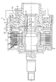
- the input casing 2 has a bottomed cylindrical shape. An opening at the rear portion (right side shown in FIG. 1) of the input casing 2 is covered with a rear casing 6.
- the input casing 2 accommodates a pilot clutch mechanism 4, a cam mechanism 5 and a main clutch mechanism 7.
- the main clutch mechanism 7 is a wet multi-plate clutch mechanism. In the main clutch mechanism 7, a large number of inner clutch plates 8 and outer clutch plates 9 are alternately arranged.
- FIG. 3 is an enlarged cross-sectional view of the DLC film 26 shown in FIG.
- the treatment layer 33 is formed by supplying ions (mainly Ar ions and H ions). Although not shown in FIG. 3, fine irregularities are formed on the surface of the treatment layer 33. That is, the surface of the treatment layer 33 is moderately roughened.
- the surface of the processing layer 33 functions as a boundary surface with the DLC film 26. Since the fine irregularities are formed on the surface, the treatment layer 33 is excellent in adhesion to the DLC film 26.
- the oil rotary vacuum pump generally has a relatively high ultimate pressure (for example, several tens to several hundreds Pa). Therefore, by adopting an oil rotary vacuum pump as the first pump 53, the inside of the processing chamber 42 after decompression does not become extremely low pressure (for example, 10 Pa or less).
- a second exhaust pipe 54 for exhausting the atmosphere in the processing chamber 42 is connected to the partition wall 41 of the processing chamber 42.
- the tip of the second exhaust pipe 54 is connected to the middle part of the first exhaust pipe 51, more specifically, between the first pump 53 and the first control valve 52.
- a second control valve 55 and a second pump 56 are interposed in this order from the processing chamber 42 side.
- the second adjustment valve 55 is for adjusting the processing pressure in the processing chamber 42 by adjusting the opening degree.
- a high vacuum pump such as a turbo molecular pump or an oil diffusion pump is employed.
- the DLC film 26 of the example was formed on the surface.
- a pretreatment process shown in FIG. 6B and a DLC deposition process shown in FIG. 6C are performed in this order.
- FIG. 9 shows the relationship between the sliding time (elapsed time from the start of the test) and the friction time in the frictional wear test.
- the argon gas and the hydrogen gas introduced into the process chamber 42 have a relatively large flow rate (the argon gas is 100 to 150 sccm, hydrogen gas is 100 to 150 sccm), and methane gas and nitrogen gas introduced into the processing chamber 42 have relatively small flow rates (methane gas is 30 to 50 sccm, nitrogen gas is 30 to 50 sccm). Therefore, in the first half of the pretreatment process (first process), the argon gas and hydrogen gas contained in the atmosphere in the processing chamber 42 have a relatively high concentration, and the concentrations of methane gas and nitrogen gas in the processing chamber 42 are relatively high.
- the DLC film 26 may contain another metal (for example, Cr, Ti, Fe, etc.), or the DLC film 26 may be used.
- the structure which does not contain any metal may be sufficient.
- carbon steel (S50C) or stainless steel can be used instead of tool steel.
Abstract
Provided are a DLC film which has good adhesiveness, even under a low-temperature environment, and a DLC film-forming method with which it is possible to form the DLC film. Also provided is a DLC film having excellent initial compatibility and a DLC film-forming method with which it is possible to form this DLC film. A first opposing surface (31) which opposes an inner clutch plate at a substrate (30) of an outer clutch plate (15) is covered by a DLC film (26). Moreover, a treatment layer (33) is formed at the surface layer section of the substrate (30). The treatment layer (33) is formed by applying a direct-current pulse voltage to the substrate (30) and generating plasma in an atmosphere containing argon gas and hydrogen gas.
Description
この発明は、DLC膜形成方法およびDLC膜に関する。
The present invention relates to a DLC film forming method and a DLC film.
たとえば、自動車の燃費を低減させるために、自動車に搭載される摺動部材の摺動抵抗の低減が求められている。そのため、摺動部材の表面を、低摩擦性および耐摩耗性(高硬度性)を有するDLC(Diamond Like Carbon)膜で被覆する構成が知られている。
DLC膜は、たとえば、直流プラズマCVD(Direct Current Plasma Chemical Vapor Deposition)法によって形成される。DLC膜の形成には、たとえば特許文献1に示す直流プラズマ方式の処理装置が用いられる。その直流プラズマ方式の処理装置において、処理室内が、炭酸水素系の原料ガス雰囲気の減圧状態で、基材に直流電圧が印加されることにより、処理室内にプラズマが発生する。そして、原料ガスがプラズマ化されて、基材の表面上にDLCの堆積層が形成される。 For example, in order to reduce the fuel consumption of automobiles, reduction of sliding resistance of sliding members mounted on automobiles is required. Therefore, a configuration is known in which the surface of the sliding member is covered with a DLC (Diamond Like Carbon) film having low friction and wear resistance (high hardness).
The DLC film is formed by, for example, a direct current plasma chemical vapor deposition (DC) method. For the formation of the DLC film, for example, a DC plasma processing apparatus shown inPatent Document 1 is used. In the DC plasma processing apparatus, plasma is generated in the processing chamber when a DC voltage is applied to the substrate while the processing chamber is in a decompressed state of a hydrogen carbonate-based source gas atmosphere. The source gas is then turned into a plasma, and a DLC deposition layer is formed on the surface of the substrate.
DLC膜は、たとえば、直流プラズマCVD(Direct Current Plasma Chemical Vapor Deposition)法によって形成される。DLC膜の形成には、たとえば特許文献1に示す直流プラズマ方式の処理装置が用いられる。その直流プラズマ方式の処理装置において、処理室内が、炭酸水素系の原料ガス雰囲気の減圧状態で、基材に直流電圧が印加されることにより、処理室内にプラズマが発生する。そして、原料ガスがプラズマ化されて、基材の表面上にDLCの堆積層が形成される。 For example, in order to reduce the fuel consumption of automobiles, reduction of sliding resistance of sliding members mounted on automobiles is required. Therefore, a configuration is known in which the surface of the sliding member is covered with a DLC (Diamond Like Carbon) film having low friction and wear resistance (high hardness).
The DLC film is formed by, for example, a direct current plasma chemical vapor deposition (DC) method. For the formation of the DLC film, for example, a DC plasma processing apparatus shown in
一方、直流プラズマCVD法によるDLCの堆積に先立って、基材の表面に窒化処理が施される。これら窒化処理とDLCの堆積層の形成とは、たとえば同一の処理装置を用いて実施される。すなわち、窒化処理では、窒素ガス雰囲気下の減圧状態で、基材に直流電圧が印加されることにより、処理室内にプラズマが発生する。そして、窒素ガスがプラズマ化されて、基材の表面に窒化層が形成される。その窒化層上に、直流プラズマCVD法によるDLCの堆積層が形成される。
On the other hand, prior to the deposition of DLC by the direct current plasma CVD method, the surface of the base material is subjected to nitriding treatment. The nitriding process and the formation of the deposited layer of DLC are performed using, for example, the same processing apparatus. That is, in the nitriding process, plasma is generated in the processing chamber by applying a DC voltage to the substrate in a reduced pressure state in a nitrogen gas atmosphere. Nitrogen gas is turned into plasma, and a nitride layer is formed on the surface of the substrate. A DLC deposition layer is formed on the nitride layer by DC plasma CVD.
特許文献1に示す直流プラズマ方式の装置は、処理中において連続してプラズマを発生させるものであるので、窒化処理およびDLC膜の堆積(形成)のための処理のいずれにおいても、処理室の温度(処理温度)が500~600℃に達する。
Since the DC plasma type apparatus shown in Patent Document 1 generates plasma continuously during processing, the temperature of the processing chamber is used in both nitriding processing and processing for depositing (forming) a DLC film. (Processing temperature) reaches 500-600 ° C.
しかしながら、処理温度が500~600℃と高温になる特許文献1の処理装置では、耐熱性を有さない材料からなる基材に対してDLC膜を形成することができない。そのため、DLC膜を成膜することが可能な基材の材料選択の幅が狭くなっている。DLC膜を低温環境下で形成できれば、基材の材料選択の幅が広がり、望ましい。そこで、本願発明者らは、300℃以下の低温環境下におけるDLC膜の形成を検討している。
However, in the processing apparatus of Patent Document 1 where the processing temperature is as high as 500 to 600 ° C., a DLC film cannot be formed on a base material made of a material that does not have heat resistance. Therefore, the range of the material selection of the base material which can form a DLC film is narrow. If the DLC film can be formed in a low temperature environment, it is desirable because the range of material selection for the base material is widened. Accordingly, the inventors of the present application are considering the formation of a DLC film in a low temperature environment of 300 ° C. or lower.
しかしながら、窒化層の形成のためには、処理温度が約500℃以上である必要があり、300℃以下の処理温度では、基材の表面に窒化層を形成することはできない。窒化層が形成されないと、DLC膜の形成後におけるDLC膜と基材との間の密着性が悪くなるおそれがある。
さらに、DLC膜は、使用初期における相手材とのなじみ性(以下、「初期なじみ性」という)が悪いという問題がある。これは、DLC膜が基材の表面状態の影響を受けた結果DLC膜の表面が粗くなっていることが一因と考えられている。そのため、本願発明者らは、DLC膜が形成される基材の表面状態を改良することにより、DLC膜の初期なじみ性を向上させることを検討している。 However, in order to form a nitride layer, the treatment temperature needs to be about 500 ° C. or higher, and a nitride layer cannot be formed on the surface of the substrate at a treatment temperature of 300 ° C. or less. If the nitride layer is not formed, the adhesion between the DLC film and the substrate after the formation of the DLC film may be deteriorated.
Furthermore, the DLC film has a problem that the conformability with the counterpart material in the initial stage of use (hereinafter referred to as “initial conformability”) is poor. This is thought to be due to the fact that the surface of the DLC film is rough as a result of the DLC film being affected by the surface condition of the substrate. Therefore, the inventors of the present application are considering improving the initial conformability of the DLC film by improving the surface state of the substrate on which the DLC film is formed.
そこで、本発明の目的の一つは、低温環境下であっても、良好な密着性を有するDLC膜、およびこのDLC膜を形成することができるDLC膜形成方法を提供することである。
また、本発明の目的の一つは、初期なじみ性の優れたDLC膜、およびこのDLC膜を形成することができるDLC膜形成方法を提供することである。 Accordingly, one of the objects of the present invention is to provide a DLC film having good adhesion even in a low temperature environment and a DLC film forming method capable of forming this DLC film.
Another object of the present invention is to provide a DLC film having excellent initial conformability and a DLC film forming method capable of forming the DLC film.
本発明のDLC膜形成方法は、処理室内で、基材の表面の少なくとも一部を被覆するDLC膜を形成する方法であって、低真空ポンプによって生成された所定の処理圧の減圧状態において実行され、直流パルス電圧を前記基材に印加して、前記処理室の内部においてアルゴンガスおよび水素系ガスを含む雰囲気中でプラズマを発生させることにより、ArイオンおよびHイオンを前記基材の表面に供給する前処理工程と、前記減圧状態において前記前処理工程後に実行され、直流パルス電圧を前記基材に印加して、前記処理室の内部において雰囲気中でプラズマを発生させることにより、前処理工程が施された後の前記基材の表面にDLCの堆積層を形成するDLC堆積工程とを含み、前記前処理工程および前記DLC堆積工程では、前記基材の温度が300℃以下になるように、当該両工程の処理時間、当該両工程における前記所定の処理圧、または当該両工程において前記基材に印加される前記直流パルス電圧の周波数、デューティ比もしくは電圧値が設定されている、DLC膜形成方法である。
The DLC film forming method of the present invention is a method of forming a DLC film that covers at least a part of the surface of a substrate in a processing chamber, and is executed in a reduced pressure state of a predetermined processing pressure generated by a low vacuum pump. And applying a DC pulse voltage to the substrate to generate plasma in an atmosphere containing argon gas and hydrogen-based gas inside the processing chamber, whereby Ar ions and H ions are applied to the surface of the substrate. A pretreatment step of supplying, and a pretreatment step performed after the pretreatment step in the reduced pressure state, by applying a direct-current pulse voltage to the substrate and generating plasma in the atmosphere inside the treatment chamber. A DLC deposition step of forming a DLC deposition layer on the surface of the base material after being applied, in the pretreatment step and the DLC deposition step, The processing time of the two steps, the predetermined processing pressure in the two steps, the frequency of the DC pulse voltage applied to the substrate in the two steps, and the duty so that the temperature of the substrate is 300 ° C. or lower. This is a DLC film forming method in which the ratio or voltage value is set.
本発明のDLC膜形成方法によると、低温環境下であっても、良好な密着性を有するDLC膜、およびこのDLC膜を形成することができる。
また、本発明のDLC膜形成方法によると、初期なじみ性の優れたDLC膜、およびこのDLC膜を形成することができるDLC膜形成方法を提供することができる。 According to the DLC film forming method of the present invention, a DLC film having good adhesion and this DLC film can be formed even in a low temperature environment.
Further, according to the DLC film forming method of the present invention, it is possible to provide a DLC film having excellent initial conformability and a DLC film forming method capable of forming the DLC film.
以下に、図面を参照して、この発明の実施形態について具体的に説明する。
尚、この明細書において、「水素系ガス」とは、水素ガスの他、炭化水素ガス、アンモニアガスなど水素原子を含むガスを包含する趣旨である。
図1は、本発明の一実施形態(第1実施形態)に係るDLC膜26が表面に形成されたアウタークラッチプレート15が組み込まれた駆動力伝達装置1の概略構成を示す断面図である。駆動力伝達装置1は、たとえば四輪駆動車に搭載されており、プロペラシャフト(図示しない)側から与えられる駆動力を、ピニオンシャフト(図示しない)に伝達するためのものである。駆動力伝達装置1は、入力ケーシング2、出力軸3、パイロットクラッチ機構部4、カム機構部5およびメインクラッチ機構部7を備えている。入力ケーシング2はプロペラシャフト(図示しない)に連結されており、出力軸3はピニオンシャフト(図示しない)に連結されている。 Embodiments of the present invention will be specifically described below with reference to the drawings.
In this specification, the “hydrogen-based gas” is intended to include a gas containing hydrogen atoms such as hydrocarbon gas and ammonia gas in addition to hydrogen gas.
FIG. 1 is a cross-sectional view showing a schematic configuration of a drivingforce transmission device 1 in which an outer clutch plate 15 having a DLC film 26 formed on the surface thereof is incorporated according to an embodiment (first embodiment) of the present invention. The driving force transmission device 1 is mounted on, for example, a four-wheel drive vehicle, and transmits driving force applied from a propeller shaft (not shown) to a pinion shaft (not shown). The driving force transmission device 1 includes an input casing 2, an output shaft 3, a pilot clutch mechanism portion 4, a cam mechanism portion 5, and a main clutch mechanism portion 7. The input casing 2 is connected to a propeller shaft (not shown), and the output shaft 3 is connected to a pinion shaft (not shown).
尚、この明細書において、「水素系ガス」とは、水素ガスの他、炭化水素ガス、アンモニアガスなど水素原子を含むガスを包含する趣旨である。
図1は、本発明の一実施形態(第1実施形態)に係るDLC膜26が表面に形成されたアウタークラッチプレート15が組み込まれた駆動力伝達装置1の概略構成を示す断面図である。駆動力伝達装置1は、たとえば四輪駆動車に搭載されており、プロペラシャフト(図示しない)側から与えられる駆動力を、ピニオンシャフト(図示しない)に伝達するためのものである。駆動力伝達装置1は、入力ケーシング2、出力軸3、パイロットクラッチ機構部4、カム機構部5およびメインクラッチ機構部7を備えている。入力ケーシング2はプロペラシャフト(図示しない)に連結されており、出力軸3はピニオンシャフト(図示しない)に連結されている。 Embodiments of the present invention will be specifically described below with reference to the drawings.
In this specification, the “hydrogen-based gas” is intended to include a gas containing hydrogen atoms such as hydrocarbon gas and ammonia gas in addition to hydrogen gas.
FIG. 1 is a cross-sectional view showing a schematic configuration of a driving
入力ケーシング2は有底円筒状をなしている。入力ケーシング2の後部(図1に示す右側)の開口は、リヤケーシング6によって覆われている。入力ケーシング2には、パイロットクラッチ機構部4、カム機構部5およびメインクラッチ機構部7が収容されている。メインクラッチ機構部7は、湿式多板式のクラッチ機構からなるものである。メインクラッチ機構部7では、多数枚のインナークラッチプレート8およびアウタークラッチプレート9が交互に配置されている。
The input casing 2 has a bottomed cylindrical shape. An opening at the rear portion (right side shown in FIG. 1) of the input casing 2 is covered with a rear casing 6. The input casing 2 accommodates a pilot clutch mechanism 4, a cam mechanism 5 and a main clutch mechanism 7. The main clutch mechanism 7 is a wet multi-plate clutch mechanism. In the main clutch mechanism 7, a large number of inner clutch plates 8 and outer clutch plates 9 are alternately arranged.
出力軸3は、リヤケーシング6の中央部を貫通し、入力ケーシング2の内部を挿通している。出力軸3は、入力ケーシング2およびリヤケーシング6に対して回転可能に設けられている。
パイロットクラッチ機構部4は、電磁コイル10、摩擦クラッチ11およびアーマチャ12を備えている。アーマチャ12は、円環状をなしており、入力ケーシング2の内周に沿って配置されている。アーマチャ12は、入力ケーシング2にスプライン嵌合されており、これにより、入力ケーシング2に対する軸方向への移動が許容されている。アーマチャ12は、摩擦クラッチ11の一方側に対向して配置されている。摩擦クラッチ11は、鉄製の2枚のアウタークラッチプレート15と、この2枚のアウタークラッチプレート15に挟まれた1枚のインナークラッチプレート16とを備えている。 Theoutput shaft 3 passes through the center of the rear casing 6 and passes through the input casing 2. The output shaft 3 is provided so as to be rotatable with respect to the input casing 2 and the rear casing 6.
Thepilot clutch mechanism 4 includes an electromagnetic coil 10, a friction clutch 11, and an armature 12. The armature 12 has an annular shape and is disposed along the inner periphery of the input casing 2. The armature 12 is spline-fitted to the input casing 2, thereby allowing movement in the axial direction relative to the input casing 2. The armature 12 is disposed to face one side of the friction clutch 11. The friction clutch 11 includes two outer clutch plates 15 made of iron and one inner clutch plate 16 sandwiched between the two outer clutch plates 15.
パイロットクラッチ機構部4は、電磁コイル10、摩擦クラッチ11およびアーマチャ12を備えている。アーマチャ12は、円環状をなしており、入力ケーシング2の内周に沿って配置されている。アーマチャ12は、入力ケーシング2にスプライン嵌合されており、これにより、入力ケーシング2に対する軸方向への移動が許容されている。アーマチャ12は、摩擦クラッチ11の一方側に対向して配置されている。摩擦クラッチ11は、鉄製の2枚のアウタークラッチプレート15と、この2枚のアウタークラッチプレート15に挟まれた1枚のインナークラッチプレート16とを備えている。 The
The
カム機構部5は、第1カム部材17および第2カム部材18を備えている。第1カム部材17および第2カム部材18は、互いに対向するように配置されている。第1カム部材17は、出力軸3に対して回転可能に設けられている。第2カム部材18は、出力軸3にスプライン嵌合されており、出力軸3と一体回転可能に設けられている。また、第2カム部材18は、出力軸3に対する軸方向への移動が許容されている。第1および第2カム部材17,18の対向面には、周方向に延びるカム溝が間隔をあけて複数形成されている。第1カム部材17と第2カム部材18との間には、ボール状のカムフォロア19がカム溝に嵌った状態で介在している。カム溝は、周方向中央部から両端部へ向かうにつれて浅くなっている。
The cam mechanism unit 5 includes a first cam member 17 and a second cam member 18. The first cam member 17 and the second cam member 18 are disposed so as to face each other. The first cam member 17 is provided to be rotatable with respect to the output shaft 3. The second cam member 18 is spline-fitted to the output shaft 3 and is provided so as to be rotatable integrally with the output shaft 3. The second cam member 18 is allowed to move in the axial direction with respect to the output shaft 3. A plurality of cam grooves extending in the circumferential direction are formed on the opposing surfaces of the first and second cam members 17 and 18 at intervals. A ball-shaped cam follower 19 is interposed between the first cam member 17 and the second cam member 18 in a state of being fitted in the cam groove. The cam groove becomes shallower from the center in the circumferential direction toward both ends.
アウタークラッチプレート15およびインナークラッチプレート16は、円環板状をなしている。2枚のアウタークラッチプレート15の間にインナークラッチプレート16が配置されている。アウタークラッチプレート15とインナークラッチプレート16とは、互いに接離可能に設けられている。アウタークラッチプレート15とインナークラッチプレート16とが互いに当接するときは、インナークラッチプレート16とアウタークラッチプレート15とが摩擦接触する。また、インナークラッチプレート16とアウタークラッチプレート15とが互いに離間した状態にあるときは、両者は接触しない。インナークラッチプレート16は、第1カム部材17の外周にスプライン嵌合されており、これにより、第1カム部材17に対する軸方向への移動が許容されている。アウタークラッチプレート15は、入力ケーシング2の内周にスプライン嵌合されており、入力ケーシング2に対する軸方向への移動が許容されている。
The outer clutch plate 15 and the inner clutch plate 16 have an annular plate shape. An inner clutch plate 16 is disposed between the two outer clutch plates 15. The outer clutch plate 15 and the inner clutch plate 16 are provided so as to be able to contact and separate from each other. When the outer clutch plate 15 and the inner clutch plate 16 are in contact with each other, the inner clutch plate 16 and the outer clutch plate 15 are in frictional contact. Further, when the inner clutch plate 16 and the outer clutch plate 15 are separated from each other, they do not contact each other. The inner clutch plate 16 is splined to the outer periphery of the first cam member 17, thereby allowing movement in the axial direction with respect to the first cam member 17. The outer clutch plate 15 is splined to the inner periphery of the input casing 2 and is allowed to move in the axial direction with respect to the input casing 2.
入力ケーシング2およびリヤケーシング6によって形成された収容室内には、潤滑油が充填されている。この潤滑油によって、パイロットクラッチ機構部4の各クラッチプレート15,16およびメインクラッチ機構部7の各クラッチプレート8,9が潤滑される。電磁コイル10に通電されていない状態では、パイロットクラッチ機構部4は非作動状態にある。そのため、メインクラッチ機構部7は非作動状態にある。このため、入力ケーシング2に入力された回転トルクは、出力軸3には伝達されず、車両は二輪駆動の駆動モードとなる。
The accommodation chamber formed by the input casing 2 and the rear casing 6 is filled with lubricating oil. With this lubricating oil, the clutch plates 15 and 16 of the pilot clutch mechanism 4 and the clutch plates 8 and 9 of the main clutch mechanism 7 are lubricated. When the electromagnetic coil 10 is not energized, the pilot clutch mechanism 4 is in an inoperative state. Therefore, the main clutch mechanism unit 7 is in an inoperative state. For this reason, the rotational torque input to the input casing 2 is not transmitted to the output shaft 3, and the vehicle is in a two-wheel drive drive mode.
電磁コイル10に通電された状態では、アーマチャ12が、電磁コイル10の吸引により電磁コイル10に向けて移動し、そのため、アーマチャ12が摩擦クラッチ11と摩擦係合するようになる。そして、アーマチャ12と摩擦クラッチ11とが摩擦係合することにより、第1カム部材17と入力ケーシング2側とが連結される。これにより、第1カム部材17は、入力ケーシング2の回転に伴い回転し、第2カム部材18に対して相対回転する。そして、カムフォロア19がカム溝の浅い箇所に乗り上げることにより、第2カム部材18がメインクラッチ機構部7側へ移動する。これにより、アウタークラッチプレート9とインナークラッチプレート8とが摩擦係合し、入力ケーシング2と出力軸3とが連結されて、入力ケーシング2に入力された回転トルクは、出力軸3に伝達される。このため、車両は四輪駆動の駆動モードになる。
When the electromagnetic coil 10 is energized, the armature 12 moves toward the electromagnetic coil 10 due to the attraction of the electromagnetic coil 10, so that the armature 12 is frictionally engaged with the friction clutch 11. Then, the armature 12 and the friction clutch 11 are frictionally engaged to connect the first cam member 17 and the input casing 2 side. Accordingly, the first cam member 17 rotates with the rotation of the input casing 2 and rotates relative to the second cam member 18. Then, when the cam follower 19 rides on a shallow portion of the cam groove, the second cam member 18 moves to the main clutch mechanism 7 side. Thereby, the outer clutch plate 9 and the inner clutch plate 8 are frictionally engaged, the input casing 2 and the output shaft 3 are connected, and the rotational torque input to the input casing 2 is transmitted to the output shaft 3. . For this reason, the vehicle is in a four-wheel drive mode.
また、電磁コイル10への電流量を変化させることにより、アーマチャ12に発生する吸引力が、電流量に比例して変化する。これが、カム機構部5によって軸方向に力に変換されて、電流量に比例した摩擦トルクが発生する。
図2は、摩擦クラッチ11の断面図である。
アウタークラッチプレート15およびインナークラッチプレート16は、工具鋼(たとえばSKH51やSKH4など)を用いて形成された基材30を備えている。アウタークラッチプレート15の基材30におけるインナークラッチプレート16と対向する第1対向面31には、クラッチプレート15,16間に残存した潤滑油を受け入れるためのメッシュ状(網目状)の潤滑油溝23が形成されている。基材30の第1対向面31は、DLC膜26で被覆されている。DLC膜26の表面には、インナークラッチプレート16と摺動する第1摺動面21が形成されている。 Further, by changing the amount of current to theelectromagnetic coil 10, the attractive force generated in the armature 12 changes in proportion to the amount of current. This is converted into a force in the axial direction by the cam mechanism unit 5, and a friction torque proportional to the amount of current is generated.
FIG. 2 is a sectional view of thefriction clutch 11.
The outerclutch plate 15 and the inner clutch plate 16 include a base material 30 formed using tool steel (for example, SKH51 or SKH4). On the first facing surface 31 of the base material 30 of the outer clutch plate 15 facing the inner clutch plate 16, a mesh-like (mesh-like) lubricating oil groove 23 for receiving the lubricating oil remaining between the clutch plates 15 and 16. Is formed. The first facing surface 31 of the substrate 30 is covered with the DLC film 26. A first sliding surface 21 that slides with the inner clutch plate 16 is formed on the surface of the DLC film 26.
図2は、摩擦クラッチ11の断面図である。
アウタークラッチプレート15およびインナークラッチプレート16は、工具鋼(たとえばSKH51やSKH4など)を用いて形成された基材30を備えている。アウタークラッチプレート15の基材30におけるインナークラッチプレート16と対向する第1対向面31には、クラッチプレート15,16間に残存した潤滑油を受け入れるためのメッシュ状(網目状)の潤滑油溝23が形成されている。基材30の第1対向面31は、DLC膜26で被覆されている。DLC膜26の表面には、インナークラッチプレート16と摺動する第1摺動面21が形成されている。 Further, by changing the amount of current to the
FIG. 2 is a sectional view of the
The outer
また、インナークラッチプレート16におけるアウタークラッチプレート15と摺動する第2摺動面32の全域には、微小幅の多数の溝25が、微小の間隔を隔てて配列されている。図2では、理解し易いように溝25を誇張して図示してあるが、溝25の幅やそのピッチは、たとえば数μm程度に設定されている。
図3は、図2に示すDLC膜26の拡大断面図である。 In addition, a large number ofgrooves 25 having a small width are arranged at a small interval in the entire area of the second sliding surface 32 that slides with the outer clutch plate 15 in the inner clutch plate 16. In FIG. 2, the grooves 25 are exaggerated for easy understanding, but the width and pitch of the grooves 25 are set to, for example, about several μm.
FIG. 3 is an enlarged cross-sectional view of theDLC film 26 shown in FIG.
図3は、図2に示すDLC膜26の拡大断面図である。 In addition, a large number of
FIG. 3 is an enlarged cross-sectional view of the
アウタークラッチプレート15における基材30の第1対向面31(基材30の表面)には、処理層33が形成されている。言い換えれば、アウタークラッチプレート15の表層部分が、処理層33によって構成されている。処理層33には、種々の元素、たとえばAr、H、CおよびNが含有されている。この処理層33上に、DLC膜26が形成されている。DLC膜26は、直流プラズマCVD法によるDLCの堆積層によって構成されている。DLC膜26の厚みは、たとえば1.0~6.0μmであり、DLC膜26のナノインデンション硬さは10~30GPa程度である。DLC膜26は、所定の比率(たとえば、10~20wt%程度)でSiを含有している。
A treatment layer 33 is formed on the first facing surface 31 (surface of the base material 30) of the base material 30 in the outer clutch plate 15. In other words, the surface layer portion of the outer clutch plate 15 is constituted by the processing layer 33. The treatment layer 33 contains various elements such as Ar, H, C and N. A DLC film 26 is formed on the processing layer 33. The DLC film 26 is composed of a DLC deposition layer formed by direct current plasma CVD. The thickness of the DLC film 26 is, for example, 1.0 to 6.0 μm, and the nanoindentation hardness of the DLC film 26 is about 10 to 30 GPa. The DLC film 26 contains Si at a predetermined ratio (for example, about 10 to 20 wt%).
処理層33は、イオン(主としてArイオンおよびHイオン)が供給されることにより形成される。図3には表れていないが、処理層33の表面には微細な凹凸が形成されている。すなわち、この処理層33の表面は適度に荒らされている。この処理層33の表面がDLC膜26との間の境界面として機能する。表面に微細な凹凸が形成されているために、この処理層33はDLC膜26との密着性に優れている。
The treatment layer 33 is formed by supplying ions (mainly Ar ions and H ions). Although not shown in FIG. 3, fine irregularities are formed on the surface of the treatment layer 33. That is, the surface of the treatment layer 33 is moderately roughened. The surface of the processing layer 33 functions as a boundary surface with the DLC film 26. Since the fine irregularities are formed on the surface, the treatment layer 33 is excellent in adhesion to the DLC film 26.
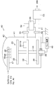
図4は、DLC膜26の形成に用いられる処理装置40の構成を示す模式的な断面図である。この処理装置40を用いて、直流パルスプラズマCVD法によりDLC膜26を作成することができる。
この処理装置40は、隔壁41で取り囲まれた処理室42を備えている。この隔壁41は、ステンレス鋼などの導電材料を用いて形成されている。処理室42内には、処理対象となる基材30(アウタークラッチプレート15)を保持するための基台43が収容されている。基台43は、基材30を下方から支持する支持プレート38と、鉛直方向に延び、支持プレート38を支持する支持軸44とを備えている。支持プレート38は水平姿勢をなしている。この実施形態では、基台43として、支持プレート38が上下方向に3つ並んで配置された3段式のものが採用されている。 FIG. 4 is a schematic cross-sectional view showing the configuration of theprocessing apparatus 40 used for forming the DLC film 26. Using this processing apparatus 40, the DLC film 26 can be formed by DC pulse plasma CVD.
Theprocessing apparatus 40 includes a processing chamber 42 surrounded by a partition wall 41. The partition wall 41 is formed using a conductive material such as stainless steel. A base 43 for holding the base material 30 (outer clutch plate 15) to be processed is accommodated in the processing chamber 42. The base 43 includes a support plate 38 that supports the base material 30 from below, and a support shaft 44 that extends in the vertical direction and supports the support plate 38. The support plate 38 has a horizontal posture. In this embodiment, a three-stage type in which three support plates 38 are arranged in the vertical direction is adopted as the base 43.
この処理装置40は、隔壁41で取り囲まれた処理室42を備えている。この隔壁41は、ステンレス鋼などの導電材料を用いて形成されている。処理室42内には、処理対象となる基材30(アウタークラッチプレート15)を保持するための基台43が収容されている。基台43は、基材30を下方から支持する支持プレート38と、鉛直方向に延び、支持プレート38を支持する支持軸44とを備えている。支持プレート38は水平姿勢をなしている。この実施形態では、基台43として、支持プレート38が上下方向に3つ並んで配置された3段式のものが採用されている。 FIG. 4 is a schematic cross-sectional view showing the configuration of the
The
また、基台43(すなわち、各支持プレート38および支持軸44)は、鋼などの導電材料を用いて形成されている。基台43には、直流のパルス電源(直流パルス電源)46が電気的に接続されている。パルス電源46からは、後で詳述するように直流パルス電圧が出力される。パルス電源46の設定電圧値は、たとえば-1000V程度に設定されている。すなわち、パルス電源46がオンされると、1000Vの負極性の直流パルス電圧が基台43に印加される。すなわち、基台43は陰極として機能する。
The base 43 (that is, each support plate 38 and the support shaft 44) is formed using a conductive material such as steel. A DC pulse power source (DC pulse power source) 46 is electrically connected to the base 43. The pulse power supply 46 outputs a DC pulse voltage as will be described in detail later. The set voltage value of the pulse power supply 46 is set to about −1000 V, for example. That is, when the pulse power supply 46 is turned on, a negative DC pulse voltage of 1000 V is applied to the base 43. That is, the base 43 functions as a cathode.
処理室42の隔壁41は、アース接続されている。隔壁41と基台43とは、絶縁部39によって絶縁されている。そのため、隔壁41はアース電位に保たれている。
また、処理室42には、基台43に支持された基材30の温度を計測するための温度センサ(図示しない)が配置されている。温度センサは、基材30の温度が予め定める低温(たとえば300℃)を超えるか否かを監視している。 Thepartition wall 41 of the processing chamber 42 is grounded. The partition wall 41 and the base 43 are insulated by an insulating portion 39. Therefore, the partition wall 41 is kept at the ground potential.
Theprocessing chamber 42 is provided with a temperature sensor (not shown) for measuring the temperature of the base material 30 supported by the base 43. The temperature sensor monitors whether or not the temperature of the base material 30 exceeds a predetermined low temperature (for example, 300 ° C.).
また、処理室42には、基台43に支持された基材30の温度を計測するための温度センサ(図示しない)が配置されている。温度センサは、基材30の温度が予め定める低温(たとえば300℃)を超えるか否かを監視している。 The
The
原料ガス導入管47は、処理室42内における基台43の上方を、水平方向に延びている。原料ガス導入管47の基台43に対向する部分には、原料ガス導入管47の長手方向に沿って配列された多数の吐出孔48が形成されている。原料ガス導入管47には、炭化水素ガスの一例としてのメタンガス(CH4)、水素ガス(H2)、アルゴンガス(Ar)、窒素ガス(N2)およびテトラメチルシランガス((Si(CH3)4)。以下、「TMS」という)が供給されるようになっている。原料ガス導入管47には、各原料ガスの供給源であるガスボンベ(図示しない)からの原料ガスを処理室に導くための複数の分岐導入管(図示しない)が接続されている。各分岐導入管(図示しない)には、ガスボンベから処理室42に導かれるガスの流量を調節するための流量調節バルブ(図示しない)が介装されている。
The source gas introduction pipe 47 extends in the horizontal direction above the base 43 in the processing chamber 42. A number of discharge holes 48 arranged along the longitudinal direction of the source gas introduction pipe 47 are formed in a portion of the source gas introduction pipe 47 facing the base 43. The raw material gas introduction pipe 47 includes methane gas (CH 4 ), hydrogen gas (H 2 ), argon gas (Ar), nitrogen gas (N 2 ), and tetramethylsilane gas ((Si (CH 3 )) as an example of hydrocarbon gas. 4 ), hereinafter referred to as “TMS”). The source gas introduction pipe 47 is connected to a plurality of branch introduction pipes (not shown) for introducing the source gas from a gas cylinder (not shown), which is a source of each source gas, to the processing chamber. Each branch introduction pipe (not shown) is provided with a flow rate adjusting valve (not shown) for adjusting the flow rate of the gas guided from the gas cylinder to the processing chamber 42.
処理室42の隔壁41には、処理室42内の雰囲気を排気するための第1排気管51が接続されている。この第1排気管51の先端は、排気設備(図示しない)に接続されている。第1排気管51の途中部には、第1調節バルブ52および第1ポンプ53が、処理室42側からこの順で介装されている。第1調節バルブ52は、開度を調節して、処理室42内の処理圧を調整するためのものである。第1ポンプ53として、たとえば油回転真空ポンプ(ロータリポンプ)やダイヤフラム真空ポンプなどの低真空ポンプが採用されている。油回転真空ポンプは、油によってロータ、ステータおよび摺動翼板などの部品の間の気密空間および無効空間の減少を図る容積移送式真空ポンプである。第1ポンプ53として採用される油回転真空ポンプとして、回転翼型油回転真空ポンプや揺動ピストン型真空ポンプを例に挙げることができる。
A first exhaust pipe 51 for exhausting the atmosphere in the processing chamber 42 is connected to the partition wall 41 of the processing chamber 42. The tip of the first exhaust pipe 51 is connected to an exhaust facility (not shown). In the middle of the first exhaust pipe 51, a first control valve 52 and a first pump 53 are interposed in this order from the processing chamber 42 side. The first adjustment valve 52 is for adjusting the processing pressure in the processing chamber 42 by adjusting the opening degree. As the first pump 53, for example, a low vacuum pump such as an oil rotary vacuum pump (rotary pump) or a diaphragm vacuum pump is employed. The oil rotary vacuum pump is a positive displacement vacuum pump that reduces an airtight space and an ineffective space between components such as a rotor, a stator, and a sliding blade with oil. Examples of the oil rotary vacuum pump employed as the first pump 53 include a rotary blade type oil rotary vacuum pump and a swing piston type vacuum pump.
回転翼型真空ポンプは、ロータに取り付けられた2枚の翼板がスプリングによって常にステータに押し付けられた状態で回転され、翼板、ロータおよびステータで囲まれた空間の容積変化によって気体輸送が行われる。また、揺動ピストン型真空ポンプは、ステータ気密部を摺動するプランジャにガイドされた円筒部の外部が偏心ロータの回転によるプランジャの上下首振り運動に伴い、ステータ内面を微小隙間に保ち、油でシールされながら回転し、プランジャ、円筒およびステータで囲まれた空間の容積変化によって気体輸送が行われる。
The rotary vane type vacuum pump is rotated with two blades attached to the rotor always pressed against the stator by a spring, and gas transport is performed by the volume change of the space surrounded by the blade plate, rotor and stator. Is called. In addition, the oscillating piston type vacuum pump keeps the inner surface of the stator in a minute gap while the outside of the cylindrical part guided by the plunger sliding on the airtight part of the stator keeps the inner surface of the stator in a fine gap as the plunger swings by the rotation of the eccentric rotor. The gas is transported by the volume change of the space surrounded by the plunger, the cylinder and the stator.
油回転真空ポンプは、一般的にその到達圧力が比較的高い(たとえば数十~数百Pa)。したがって、第1ポンプ53として油回転真空ポンプを採用することにより、減圧後の処理室42内が極めて低圧(たとえば10Pa以下)になることはない。
処理室42の隔壁41には、処理室42内の雰囲気を排気するための第2排気管54が接続されている。この第2排気管54の先端は、第1排気管51の途中部、より詳しくは第1ポンプ53と第1調節バルブ52との間に接続されている。第2排気管54の途中部には、第2調節バルブ55および第2ポンプ56が、処理室42側からこの順で介装されている。第2調節バルブ55は、開度を調節して、処理室42内の処理圧を調整するためのものである。第2ポンプ56としては、たとえばターボ分子ポンプや油拡散ポンプなどの高真空ポンプが採用されている。 The oil rotary vacuum pump generally has a relatively high ultimate pressure (for example, several tens to several hundreds Pa). Therefore, by adopting an oil rotary vacuum pump as thefirst pump 53, the inside of the processing chamber 42 after decompression does not become extremely low pressure (for example, 10 Pa or less).
Asecond exhaust pipe 54 for exhausting the atmosphere in the processing chamber 42 is connected to the partition wall 41 of the processing chamber 42. The tip of the second exhaust pipe 54 is connected to the middle part of the first exhaust pipe 51, more specifically, between the first pump 53 and the first control valve 52. In the middle of the second exhaust pipe 54, a second control valve 55 and a second pump 56 are interposed in this order from the processing chamber 42 side. The second adjustment valve 55 is for adjusting the processing pressure in the processing chamber 42 by adjusting the opening degree. As the second pump 56, for example, a high vacuum pump such as a turbo molecular pump or an oil diffusion pump is employed.
処理室42の隔壁41には、処理室42内の雰囲気を排気するための第2排気管54が接続されている。この第2排気管54の先端は、第1排気管51の途中部、より詳しくは第1ポンプ53と第1調節バルブ52との間に接続されている。第2排気管54の途中部には、第2調節バルブ55および第2ポンプ56が、処理室42側からこの順で介装されている。第2調節バルブ55は、開度を調節して、処理室42内の処理圧を調整するためのものである。第2ポンプ56としては、たとえばターボ分子ポンプや油拡散ポンプなどの高真空ポンプが採用されている。 The oil rotary vacuum pump generally has a relatively high ultimate pressure (for example, several tens to several hundreds Pa). Therefore, by adopting an oil rotary vacuum pump as the
A
図5は、パルス電源46から出力される直流パルス電圧の波形を示す図である。直流パルス電圧の設定電圧値は、たとえば-1000V程度の値に設定されている。パルス電源46からパルス状の電圧が出力されるので、直流パルス電圧が係る高電圧であっても、処理室42内に異常放電は生じない。
直流パルス電圧のパルス周期は、パルスの周波数fの逆数(1/f)で表すことができる。直流パルス電圧の印加時間(直流パルス電圧のパルス幅)をτとすると、デューティ比は、印加時間をパルス周期で除した値であり、以下の(1)式で表すことができる。
デューティ比=τ×f ・・・(1)
ところで、基材30とDLC膜26との間の密着性を向上させるために、DLC堆積前の基材30の表面に、通常、窒化処理が施される。しかしながら、基材30の表面に窒化処理を施すためには、基材30が収容される処理室42内を、500~600℃以上の高温環境下にする必要がある。処理装置40は300℃以下の低温環境下(たとえば200℃程度)でDLC膜26を形成するための装置であるから、この処理装置40を用いて基材30の表面に窒化処理を施すことはできない。そのため、後述する前処理によって、基材30の表層部分に処理層33(図3参照)を形成し、これにより、DLC堆積後における基材30とDLC膜26との間の密着性を向上させている。この実施形態では、処理装置40を用いて処理層33およびDLC膜26の形成が行われている。 FIG. 5 is a diagram showing a waveform of a DC pulse voltage output from thepulse power supply 46. The set voltage value of the DC pulse voltage is set to a value of about −1000 V, for example. Since a pulsed voltage is output from the pulse power supply 46, even if the DC pulse voltage is a high voltage, abnormal discharge does not occur in the processing chamber 42.
The pulse period of the DC pulse voltage can be expressed by the reciprocal (1 / f) of the pulse frequency f. When the application time of the DC pulse voltage (pulse width of the DC pulse voltage) is τ, the duty ratio is a value obtained by dividing the application time by the pulse period, and can be expressed by the following equation (1).
Duty ratio = τ × f (1)
Incidentally, in order to improve the adhesion between thebase material 30 and the DLC film 26, the surface of the base material 30 before DLC deposition is usually subjected to nitriding treatment. However, in order to perform nitriding treatment on the surface of the base material 30, the inside of the processing chamber 42 in which the base material 30 is accommodated needs to be in a high temperature environment of 500 to 600 ° C. or more. Since the processing apparatus 40 is an apparatus for forming the DLC film 26 in a low temperature environment of 300 ° C. or lower (for example, about 200 ° C.), it is possible to perform nitriding treatment on the surface of the substrate 30 using the processing apparatus 40. Can not. For this reason, a treatment layer 33 (see FIG. 3) is formed on the surface layer portion of the base material 30 by a pre-treatment described later, thereby improving the adhesion between the base material 30 and the DLC film 26 after the DLC deposition. ing. In this embodiment, the processing layer 33 and the DLC film 26 are formed using the processing apparatus 40.
直流パルス電圧のパルス周期は、パルスの周波数fの逆数(1/f)で表すことができる。直流パルス電圧の印加時間(直流パルス電圧のパルス幅)をτとすると、デューティ比は、印加時間をパルス周期で除した値であり、以下の(1)式で表すことができる。
デューティ比=τ×f ・・・(1)
ところで、基材30とDLC膜26との間の密着性を向上させるために、DLC堆積前の基材30の表面に、通常、窒化処理が施される。しかしながら、基材30の表面に窒化処理を施すためには、基材30が収容される処理室42内を、500~600℃以上の高温環境下にする必要がある。処理装置40は300℃以下の低温環境下(たとえば200℃程度)でDLC膜26を形成するための装置であるから、この処理装置40を用いて基材30の表面に窒化処理を施すことはできない。そのため、後述する前処理によって、基材30の表層部分に処理層33(図3参照)を形成し、これにより、DLC堆積後における基材30とDLC膜26との間の密着性を向上させている。この実施形態では、処理装置40を用いて処理層33およびDLC膜26の形成が行われている。 FIG. 5 is a diagram showing a waveform of a DC pulse voltage output from the
The pulse period of the DC pulse voltage can be expressed by the reciprocal (1 / f) of the pulse frequency f. When the application time of the DC pulse voltage (pulse width of the DC pulse voltage) is τ, the duty ratio is a value obtained by dividing the application time by the pulse period, and can be expressed by the following equation (1).
Duty ratio = τ × f (1)
Incidentally, in order to improve the adhesion between the
図6A~Cは、処理層33およびDLC膜26の形成方法を工程順に示す図解的な断面図である。以下、図6A~Cおよび図3を参照して説明する。以下、アウタークラッチプレート15を、処理対象の基材30として説明する。この場合、基材30の表面が第1対向面31である(図6A参照)。
まず、処理対象の基材30は、処理室42内に搬入されて、支持プレート38上に載置される。これにより、基材30が基台43に保持される。基材30の処理室42への収容後、処理室42内が密閉される。処理室42が密閉され、処理室42内が減圧される。具体的には、第1調整バルブ52が開かれて第1ポンプ53のみが駆動され、処理室42内が粗引きされる。第1ポンプ53の駆動開始後予め定める第1所定時間が経過すると、第1調整バルブ52が閉じられ、第2調整バルブ55が開かれて、第2ポンプ56も駆動開始される。そして、第1ポンプ53および第2ポンプ56が予め定める第2所定時間だけ駆動されて、処理室42内が減圧される。第2所定時間の経過後、第2調整バルブ55が閉じられて、第2ポンプ56の駆動が停止される。 6A to 6C are schematic sectional views showing a method of forming theprocessing layer 33 and the DLC film 26 in the order of steps. Hereinafter, a description will be given with reference to FIGS. 6A to 6C and FIG. Hereinafter, the outer clutch plate 15 will be described as the base material 30 to be processed. In this case, the surface of the base material 30 is the first facing surface 31 (see FIG. 6A).
First, thebase material 30 to be processed is carried into the processing chamber 42 and placed on the support plate 38. Thereby, the base material 30 is held on the base 43. After the base material 30 is accommodated in the processing chamber 42, the inside of the processing chamber 42 is sealed. The processing chamber 42 is sealed, and the inside of the processing chamber 42 is depressurized. Specifically, the first adjustment valve 52 is opened, only the first pump 53 is driven, and the inside of the processing chamber 42 is roughed. When a predetermined first predetermined time elapses after driving of the first pump 53, the first adjusting valve 52 is closed, the second adjusting valve 55 is opened, and the second pump 56 is also started to drive. Then, the first pump 53 and the second pump 56 are driven for a predetermined second predetermined time, and the inside of the processing chamber 42 is decompressed. After the elapse of the second predetermined time, the second adjustment valve 55 is closed and the driving of the second pump 56 is stopped.
まず、処理対象の基材30は、処理室42内に搬入されて、支持プレート38上に載置される。これにより、基材30が基台43に保持される。基材30の処理室42への収容後、処理室42内が密閉される。処理室42が密閉され、処理室42内が減圧される。具体的には、第1調整バルブ52が開かれて第1ポンプ53のみが駆動され、処理室42内が粗引きされる。第1ポンプ53の駆動開始後予め定める第1所定時間が経過すると、第1調整バルブ52が閉じられ、第2調整バルブ55が開かれて、第2ポンプ56も駆動開始される。そして、第1ポンプ53および第2ポンプ56が予め定める第2所定時間だけ駆動されて、処理室42内が減圧される。第2所定時間の経過後、第2調整バルブ55が閉じられて、第2ポンプ56の駆動が停止される。 6A to 6C are schematic sectional views showing a method of forming the
First, the
この実施形態では、DLC膜26の形成(DLC堆積工程)に先立って、基材30の表面に前処理工程が実行される(図6B参照)。
処理室42内の減圧後、原料ガス導入管47が開かれて、種々の原料ガス(水素ガスおよびアルゴンガス)が処理室42内に導入される。水素ガスおよびアルゴンガスの流量は共に100~300sccmである。各原料ガスの流量は、流量調節バルブ(図示しない)によって調節される。また、第1ポンプ53が駆動されつつ第1調節バルブ52によって開度が調節されることにより、処理室42内が所定の処理圧(たとえば100Pa)まで減圧され、その減圧状態が維持される。 In this embodiment, prior to the formation of the DLC film 26 (DLC deposition step), a pretreatment step is performed on the surface of the substrate 30 (see FIG. 6B).
After the pressure in theprocessing chamber 42 is reduced, the source gas introduction pipe 47 is opened, and various source gases (hydrogen gas and argon gas) are introduced into the processing chamber 42. The flow rates of hydrogen gas and argon gas are both 100 to 300 sccm. The flow rate of each source gas is adjusted by a flow rate adjusting valve (not shown). Further, the opening degree is adjusted by the first adjustment valve 52 while the first pump 53 is driven, whereby the inside of the processing chamber 42 is reduced to a predetermined processing pressure (for example, 100 Pa), and the reduced pressure state is maintained.
処理室42内の減圧後、原料ガス導入管47が開かれて、種々の原料ガス(水素ガスおよびアルゴンガス)が処理室42内に導入される。水素ガスおよびアルゴンガスの流量は共に100~300sccmである。各原料ガスの流量は、流量調節バルブ(図示しない)によって調節される。また、第1ポンプ53が駆動されつつ第1調節バルブ52によって開度が調節されることにより、処理室42内が所定の処理圧(たとえば100Pa)まで減圧され、その減圧状態が維持される。 In this embodiment, prior to the formation of the DLC film 26 (DLC deposition step), a pretreatment step is performed on the surface of the substrate 30 (see FIG. 6B).
After the pressure in the
次いで、処理室42内のたとえば100Paの減圧状態が維持されつつ、基台43に負極性の約1000Vの直流パルス電圧が印加される。この直流パルス電圧の周波数は200Hz以上(たとえば、1000Hz)であり、かつデューティ比が5%以上(たとえば、50%)である。これにより、アース電位に保たれている隔壁41と基台43(基材30)との間に、約1000Vの電位差が生じ、処理室42内にプラズマが発生する。プラズマの発生により、基材30の表面(第1対向面31)が200℃程度まで昇温される。プラズマによって処理室42内の原料ガスがプラズマ化して、処理室42内にイオン・ラジカルが生成され、浮遊する。そして、これらのイオン・ラジカルが基材30の表面に供給される。基台43に印加されるのが1000Vの高電圧であるので、これらのイオン・ラジカル(たとえばHイオン、Arイオン)が強い力で基材30の表面に打ち付けられる。これにより、基材30の表面が適度に荒らされ当該表面に凹凸が形成されて、基材30の表面が改質される。パルス電源46のオンから予め定める処理時間(たとえば、30分間)が経過すると、パルス電源46がオフされて、処理室42内における放電が終了する。
Next, a negative DC pulse voltage of about 1000 V is applied to the base 43 while maintaining a reduced pressure state of, for example, 100 Pa in the processing chamber 42. The frequency of the DC pulse voltage is 200 Hz or more (for example, 1000 Hz), and the duty ratio is 5% or more (for example, 50%). As a result, a potential difference of about 1000 V is generated between the partition wall 41 maintained at the ground potential and the base 43 (base material 30), and plasma is generated in the processing chamber. Due to the generation of the plasma, the surface of the base material 30 (the first facing surface 31) is heated to about 200 ° C. The source gas in the processing chamber 42 is turned into plasma by the plasma, and ions and radicals are generated in the processing chamber 42 and float. Then, these ions and radicals are supplied to the surface of the substrate 30. Since a high voltage of 1000 V is applied to the base 43, these ions and radicals (for example, H ions and Ar ions) are struck against the surface of the substrate 30 with a strong force. Thereby, the surface of the base material 30 is moderately roughened, irregularities are formed on the surface, and the surface of the base material 30 is modified. When a predetermined processing time (for example, 30 minutes) elapses after the pulse power source 46 is turned on, the pulse power source 46 is turned off and the discharge in the processing chamber 42 is finished.
また、Hイオン・ラジカルが基材30の表面の周囲に浮遊しているので、処理室42内でプラズマが発生することに伴って基材30の表面に水酸基(OH-)が出現するが、処理室42内に浮遊するHイオンは、その還元作用により、基材30の表面から現れる水酸基を捕獲する。このため、基材30の表面から出現する水酸基が、基材30の表面に付着することを防止することができる。すなわち、Hイオンによって基材30の表面に存在する不純物を除去することができ、これにより基材30の表面が洗浄される。これら一連の前処理により、基材30の表面に処理層33が形成される。
Further, since H ions / radicals are floating around the surface of the base material 30, hydroxyl groups (OH − ) appear on the surface of the base material 30 as plasma is generated in the processing chamber 42. The H ions floating in the processing chamber 42 capture hydroxyl groups appearing from the surface of the base material 30 by the reduction action. For this reason, it is possible to prevent hydroxyl groups appearing from the surface of the substrate 30 from adhering to the surface of the substrate 30. That is, impurities existing on the surface of the base material 30 can be removed by H ions, whereby the surface of the base material 30 is washed. Through these series of pretreatments, the treatment layer 33 is formed on the surface of the substrate 30.
前処理工程に次いで、図6Cに示すように、基材30の表面(第1対向面31)にDLC膜26が形成される(DLC堆積工程が実行される)。
前処理工程の終了後、処理室42内にメタンガスおよびTMSガスが導入されると共に、水素ガスおよびアルゴンガスの流量が調整される。メタンガス、水素ガス、アルゴンガスおよびTMSガスの流量は、それぞれ、100(sccm)、60(sccm)、60(sccm)および6(sccm)である。 Following the pretreatment step, as shown in FIG. 6C, theDLC film 26 is formed on the surface (first opposing surface 31) of the base material 30 (the DLC deposition step is performed).
After completion of the pretreatment process, methane gas and TMS gas are introduced into theprocessing chamber 42, and the flow rates of hydrogen gas and argon gas are adjusted. The flow rates of methane gas, hydrogen gas, argon gas, and TMS gas are 100 (sccm), 60 (sccm), 60 (sccm), and 6 (sccm), respectively.
前処理工程の終了後、処理室42内にメタンガスおよびTMSガスが導入されると共に、水素ガスおよびアルゴンガスの流量が調整される。メタンガス、水素ガス、アルゴンガスおよびTMSガスの流量は、それぞれ、100(sccm)、60(sccm)、60(sccm)および6(sccm)である。 Following the pretreatment step, as shown in FIG. 6C, the
After completion of the pretreatment process, methane gas and TMS gas are introduced into the
次いで、処理室42内のたとえば100Paの減圧状態が維持されつつ、基台43に負極性の約1000Vの直流パルス電圧が印加される。この直流パルス電圧の周波数は200Hz以上(たとえば1000Hz)であり、かつデューティ比が5%以上(たとえは50%)である。これにより、アース電位に保たれている隔壁41と基台43(基材30)との間に約1000Vの電位差が生じ、処理室42内でプラズマが発生する。これにより、基材30の表面が200℃程度まで昇温される。処理室42内にプラズマが放射されることにより、処理室42内のメタンガスおよびTMSがプラズマ化して、処理室42内に、イオン・ラジカルが生成され、浮遊するようになる。そして、処理室42内で生じる化学反応により、Siを含有するDLCが基材30の表面上に堆積し、堆積層をなすようになる。これにより、基材30の表面上にDLC膜26が形成される(DLC堆積工程)。
Next, a negative DC pulse voltage of about 1000 V is applied to the base 43 while maintaining a reduced pressure state of, for example, 100 Pa in the processing chamber 42. The frequency of the DC pulse voltage is 200 Hz or more (for example, 1000 Hz), and the duty ratio is 5% or more (for example, 50%). As a result, a potential difference of about 1000 V is generated between the partition wall 41 maintained at the ground potential and the base 43 (base material 30), and plasma is generated in the processing chamber. Thereby, the surface of the base material 30 is heated to about 200 ° C. By radiating plasma into the processing chamber 42, methane gas and TMS in the processing chamber 42 are turned into plasma, and ions and radicals are generated and float in the processing chamber 42. A DLC containing Si is deposited on the surface of the base material 30 by a chemical reaction occurring in the processing chamber 42 to form a deposited layer. Thereby, the DLC film 26 is formed on the surface of the base material 30 (DLC deposition process).
パルス電源46の電源供給の開始から予め定める処理時間(たとえば45分間)が経過すると、パルス電源46からの電源供給が停止されて、処理室42内における放電が終了する。そして、減圧下で常温まで冷却された後、基材30が処理室42内から搬出される。これにより、アウタークラッチプレート15の第1対向面31に、DLC膜26が形成される。
When a predetermined processing time (for example, 45 minutes) elapses from the start of the power supply of the pulse power supply 46, the power supply from the pulse power supply 46 is stopped and the discharge in the processing chamber 42 is finished. And after cooling to normal temperature under pressure reduction, the base material 30 is carried out from the process chamber 42 inside. As a result, the DLC film 26 is formed on the first facing surface 31 of the outer clutch plate 15.
次に、実施例および比較例1~3について説明する。
図6A~Cに示すDLC形成方法を用いて、SKH4製の基板(25mm×25mm×5mm、触針式の表面粗さ測定に基づく算術平均粗さRaが0.004μm)からなる基材30の表面に実施例のDLC膜26を作成した。このDLC膜26の作成のために、図6Bに示す前処理工程と、図6Cに示すDLC堆積工程とが、この順で実行される。 Next, examples and comparative examples 1 to 3 will be described.
Asubstrate 30 made of SKH4 substrate (25 mm × 25 mm × 5 mm, arithmetic average roughness Ra based on stylus surface roughness measurement is 0.004 μm) using the DLC formation method shown in FIGS. 6A to 6C. The DLC film 26 of the example was formed on the surface. In order to create the DLC film 26, a pretreatment process shown in FIG. 6B and a DLC deposition process shown in FIG. 6C are performed in this order.
図6A~Cに示すDLC形成方法を用いて、SKH4製の基板(25mm×25mm×5mm、触針式の表面粗さ測定に基づく算術平均粗さRaが0.004μm)からなる基材30の表面に実施例のDLC膜26を作成した。このDLC膜26の作成のために、図6Bに示す前処理工程と、図6Cに示すDLC堆積工程とが、この順で実行される。 Next, examples and comparative examples 1 to 3 will be described.
A
また、図6A~Cに近似する態様のDLC形成方法を用いて、SKH4製の基板(25mm×25mm×5mm、触針式の表面粗さ測定に基づく算術平均粗さRaが0.004μm)からなる基材の表面に比較例1~3のDLC膜を形成した。実施例におけるDLC膜26の形成と比較例1~3におけるDLC膜の形成とは、前処理工程における処理ガス種または処理圧が異なっている。実施例および比較例1,3の場合における前処理の処理条件は、表1に示している。また、実施例および比較例1~3の場合の前処理工程およびDLC堆積工程は、図4に示す処理装置40を用いて実行される。なお、処理装置40として、処理室42内の処理領域(有効に処理できる領域)がφ300mm、高さ300mmのものを用いた。また、実施例で用いられる基材30および比較例1~3で用いられる基材の表面には、それぞれ研磨による鏡面加工が施されている。
In addition, using a DLC formation method similar to FIGS. 6A to 6C, from a SKH4 substrate (25 mm × 25 mm × 5 mm, arithmetic average roughness Ra based on stylus surface roughness measurement is 0.004 μm). The DLC films of Comparative Examples 1 to 3 were formed on the surface of the base material. The formation of the DLC film 26 in the example and the formation of the DLC film in Comparative Examples 1 to 3 are different in processing gas type or processing pressure in the pretreatment process. Table 1 shows the preconditioning conditions for the examples and comparative examples 1 and 3. Further, the pretreatment process and the DLC deposition process in the case of the example and the comparative examples 1 to 3 are performed using the processing apparatus 40 shown in FIG. In addition, as the processing apparatus 40, the processing area (area which can be effectively processed) in the processing chamber 42 is φ300 mm and the height is 300 mm. Further, the surfaces of the base material 30 used in the examples and the base materials used in Comparative Examples 1 to 3 are each subjected to mirror finishing by polishing.

実施例では、図6Bに示す前処理工程において、処理室42内の雰囲気にアルゴンガスおよび水素ガスの双方が含まれる場合を示している。処理室42内に供給されるアルゴンガスと水素ガスとの流量比は、1:1である。前処理の条件としては、直流パルス電圧の電圧値が1000V(負極性)であり、直流パルス電圧のパルス周波数が1000(Hz)であり、直流パルス電圧のデューティ比が30%である。また、前処理工程における処理圧が200(Pa)である。
In the embodiment, the case where both the argon gas and the hydrogen gas are included in the atmosphere in the processing chamber 42 in the pretreatment step shown in FIG. 6B is shown. The flow rate ratio of argon gas and hydrogen gas supplied into the processing chamber 42 is 1: 1. As preconditions, the voltage value of the DC pulse voltage is 1000 V (negative polarity), the pulse frequency of the DC pulse voltage is 1000 (Hz), and the duty ratio of the DC pulse voltage is 30%. The processing pressure in the pretreatment process is 200 (Pa).
比較例1が実施例と相違する点は、図6Bに示す前処理工程において、処理室42内の雰囲気に水素ガスが含まれず、アルゴンガスだけが含まれる点である。また、比較例2が実施例と相違する点は、図6Bに示す前処理工程において、処理室42内の雰囲気にアルゴンガスが含まれず、水素ガスだけが含まれる点である。比較例1および比較例2において、前処理工程における処理圧、前処理工程における直流パルス電圧の電圧値、デューティ比および周波数、ならびに前処理の処理時間は、実施例の場合と同じである。
Comparative Example 1 is different from the Example in that, in the pretreatment process shown in FIG. 6B, the atmosphere in the treatment chamber 42 does not contain hydrogen gas but contains only argon gas. Further, the comparative example 2 is different from the embodiment in that, in the pretreatment step shown in FIG. 6B, the atmosphere in the processing chamber 42 does not contain argon gas but contains only hydrogen gas. In Comparative Example 1 and Comparative Example 2, the processing pressure in the preprocessing step, the voltage value of the DC pulse voltage, the duty ratio and frequency in the preprocessing step, and the processing time of the preprocessing are the same as those in the example.
比較例3が、実施例と相違する点は、前処理工程における処理圧が200(Pa)ではなく50(Pa)である点である。比較例3において、前処理工程における処理ガスの流量比、前処理工程における直流パルス電圧の電圧値、デューティ比および周波数、ならびに前処理の処理時間は、実施例の場合と同じである。
実施例のDLC膜26、および比較例1~3のDLC膜に対して剥離試験を行った。DLC膜26および比較例1,2のDLC膜に対して剥離試験を行った場合の結果を図7および表1に示す。また、表1には、比較例3のDLC膜に対して剥離試験を行った場合の結果を示す。 The comparative example 3 is different from the example in that the processing pressure in the pretreatment process is 50 (Pa) instead of 200 (Pa). In Comparative Example 3, the flow rate ratio of the processing gas in the pretreatment process, the voltage value of the DC pulse voltage, the duty ratio and the frequency in the pretreatment process, and the pretreatment time are the same as in the example.
A peel test was performed on theDLC film 26 of the example and the DLC films of comparative examples 1 to 3. FIG. 7 and Table 1 show the results when a peel test was performed on the DLC film 26 and the DLC films of Comparative Examples 1 and 2. Table 1 shows the results when a peel test was performed on the DLC film of Comparative Example 3.
実施例のDLC膜26、および比較例1~3のDLC膜に対して剥離試験を行った。DLC膜26および比較例1,2のDLC膜に対して剥離試験を行った場合の結果を図7および表1に示す。また、表1には、比較例3のDLC膜に対して剥離試験を行った場合の結果を示す。 The comparative example 3 is different from the example in that the processing pressure in the pretreatment process is 50 (Pa) instead of 200 (Pa). In Comparative Example 3, the flow rate ratio of the processing gas in the pretreatment process, the voltage value of the DC pulse voltage, the duty ratio and the frequency in the pretreatment process, and the pretreatment time are the same as in the example.
A peel test was performed on the
実施例のDLC膜26の剥離開始荷重(表1に示す「密着力」)は約14Nである。比較例1のDLC膜の剥離開始荷重は25.7Nであるが、比較例2のDLC膜は、試験開始直後に剥離してしまい、剥離開始荷重を計測することができなかった。これにより、実施例では、基材30とDLC膜26との間の密着性が良好であることがわかる。
次に、実施例のDLC膜26の表面粗さおよび比較例1~3のDLC膜の表面粗さについて説明する。 The peeling start load (“adhesion force” shown in Table 1) of theDLC film 26 of the example is about 14N. Although the peeling start load of the DLC film of Comparative Example 1 was 25.7 N, the DLC film of Comparative Example 2 peeled immediately after the start of the test, and the peeling start load could not be measured. Thereby, in an Example, it turns out that the adhesiveness between the base material 30 and the DLC film 26 is favorable.
Next, the surface roughness of theDLC film 26 of the example and the surface roughness of the DLC films of Comparative Examples 1 to 3 will be described.
次に、実施例のDLC膜26の表面粗さおよび比較例1~3のDLC膜の表面粗さについて説明する。 The peeling start load (“adhesion force” shown in Table 1) of the
Next, the surface roughness of the
実施例のDLC膜26の表面粗さおよび比較例1,3のDLC膜の表面の粗さを、それぞれ、触針式の表面粗さ測定およびSPMによる表面粗さ測定の双方によって測定した。各測定結果を表1に示す。また、比較例2のDLC膜における触針式の表面粗さ測定に基づく算術平均粗さRaを測定した。実施例のDLC膜26および比較例1,2のDLC膜における触針式の表面粗さ測定に基づく算術平均粗さRaを図8に示す。
The surface roughness of the DLC film 26 of the example and the surface roughness of the DLC film of Comparative Examples 1 and 3 were measured by both the stylus type surface roughness measurement and the surface roughness measurement by SPM, respectively. Table 1 shows the measurement results. Moreover, arithmetic average roughness Ra based on the stylus type surface roughness measurement in the DLC film of Comparative Example 2 was measured. FIG. 8 shows the arithmetic average roughness Ra based on the stylus type surface roughness measurement in the DLC film 26 of the example and the DLC films of comparative examples 1 and 2.
実施例では、触針式の表面粗さ測定に基づく算術平均粗さRaは0.01μmであり、触針式の表面粗さ測定に基づく十点平均粗さRzJISは0.1μmである。これに対して、比較例1~3における触針式の表面粗さ測定に基づく算術平均粗さRaは、いずれも0.01μmを上回っている。また、比較例1,3における触針式の表面粗さ測定に基づく十点平均粗さRzJISは0.1μmを上回っている。
In the examples, the arithmetic average roughness Ra based on the stylus type surface roughness measurement is 0.01 μm, and the ten-point average roughness RzJIS based on the stylus type surface roughness measurement is 0.1 μm. On the other hand, the arithmetic average roughness Ra based on the stylus type surface roughness measurement in Comparative Examples 1 to 3 exceeds 0.01 μm. Further, the ten-point average roughness RzJIS based on the stylus type surface roughness measurement in Comparative Examples 1 and 3 exceeds 0.1 μm.
また、実施例では、SPMによる表面粗さ測定に基づく算術平均粗さRaが7nmであり、SPMによる表面粗さ測定に基づく十点平均粗さRzJISが121nmである。これに対し、比較例1,3におけるSPMによる表面粗さ測定に基づく算術平均粗さRaは、それぞれ11.4nmおよび10.0nmである。また、比較例1,3におけるSPMによる表面粗さ測定に基づく十点平均粗さRzJISが、それぞれ101nmおよび243nmである。すなわち、実施例は、SPMによる表面粗さ測定に基づく算術平均粗さRaが10nm以下で、かつSPMによる表面粗さ測定に基づく十点平均粗さRzJISが150nm以下であるが、比較例1は、SPMによる表面粗さ測定に基づく算術平均粗さRaが10nmを上回っており、また、比較例3は、SPMによる表面粗さ測定に基づく十点平均粗さRzJISが150nmを上回っている。
In the examples, the arithmetic average roughness Ra based on the surface roughness measurement by SPM is 7 nm, and the ten-point average roughness RzJIS based on the surface roughness measurement by SPM is 121 nm. On the other hand, arithmetic average roughness Ra based on the surface roughness measurement by SPM in Comparative Examples 1 and 3 is 11.4 nm and 10.0 nm, respectively. Moreover, the ten-point average roughness RzJIS based on the surface roughness measurement by SPM in Comparative Examples 1 and 3 is 101 nm and 243 nm, respectively. That is, in the examples, the arithmetic average roughness Ra based on the surface roughness measurement by SPM is 10 nm or less, and the ten-point average roughness RzJIS based on the surface roughness measurement by SPM is 150 nm or less. The arithmetic average roughness Ra based on the surface roughness measurement by SPM exceeds 10 nm, and in Comparative Example 3, the ten-point average roughness RzJIS based on the surface roughness measurement by SPM exceeds 150 nm.
そして、以上の測定結果から、実施例のDLC膜26、比較例1,3のDLC膜の中では、実施例のDLC膜26の表面が最も平滑化されていることがわかる。また、各DLC膜の表面粗さの4つの表面粗さの値を総合的に勘案することにより、比較例3のDLC膜の表面の方が、比較例1のDLC膜の表面よりも粗いことがわかる。
次に、実施例のDLC膜26の表面粗さおよび比較例1~3のDLC膜の摩擦磨耗特性について説明する。 From the above measurement results, it can be seen that, among theDLC film 26 of the example and the DLC films of comparative examples 1 and 3, the surface of the DLC film 26 of the example is smoothed most. Also, by comprehensively considering the four surface roughness values of the surface roughness of each DLC film, the surface of the DLC film of Comparative Example 3 is rougher than the surface of the DLC film of Comparative Example 1 I understand.
Next, the surface roughness of theDLC film 26 of the example and the frictional wear characteristics of the DLC films of Comparative Examples 1 to 3 will be described.
次に、実施例のDLC膜26の表面粗さおよび比較例1~3のDLC膜の摩擦磨耗特性について説明する。 From the above measurement results, it can be seen that, among the
Next, the surface roughness of the
実施例のDLC膜26、ならびに比較例1および比較例3のDLC膜に対して摩擦磨耗試験を行った。試験装置として、ボールオンプレート往復動摩擦係数試験機を用いた。このボールオンプレート往復動摩擦係数試験機では、相手材にたとえばφ4.8mmの鋼球(軸受鋼球。たとえばSUJ2製)が用いられている。そして、前述の各基材(実施例のDLC膜26が形成された基材30、ならびに比較例1および比較例3のDLC膜が形成された基材)を試験片としてセットし、速度2Hz、ストローク10mmおよび荷重10Nの試験条件で、無潤滑下で60分間(3600sec)の摩擦摩耗試験を行った。摩擦摩耗試験中は、1secに1回の割合で摩擦係数の測定を行った。摩擦摩耗試験におけるすべり時間(試験開始からの経過時間)と摩擦時間との関係を図9に示す。
Friction and wear tests were performed on the DLC film 26 of the example and the DLC films of comparative example 1 and comparative example 3. A ball-on-plate reciprocating friction coefficient tester was used as a test apparatus. In this ball-on-plate reciprocating friction coefficient testing machine, for example, a steel ball having a diameter of 4.8 mm (bearing steel ball, for example, manufactured by SUJ2) is used as a counterpart material. Then, each of the aforementioned base materials (the base material 30 on which the DLC film 26 of the example was formed and the base material on which the DLC film of the comparative example 1 and the comparative example 3 was formed) was set as a test piece, and the speed was 2 Hz. Under the test conditions of a stroke of 10 mm and a load of 10 N, a frictional wear test was performed for 60 minutes (3600 seconds) without lubrication. During the frictional wear test, the coefficient of friction was measured once every 1 sec. FIG. 9 shows the relationship between the sliding time (elapsed time from the start of the test) and the friction time in the frictional wear test.
図9に示すように、実施例および比較例1,3では、摩擦係数は最終的に0.04~0.05の低値を示したが、その低値に至る過程でそれぞれ異なる挙動を示した。なお、図9において摩擦係数が所定の低値(0.04~0.05)に達し、その低値で定常化するまでの時間、すなわち試験開始からDLC膜が相手材になじむまでの期間(以下、単に「なじみ終了までの時間」という)を矢印で示している。
As shown in FIG. 9, in the examples and comparative examples 1 and 3, the friction coefficient finally showed a low value of 0.04 to 0.05, but different behaviors were shown in the process of reaching the low value. It was. In FIG. 9, the time until the friction coefficient reaches a predetermined low value (0.04 to 0.05) and stabilizes at the low value, that is, the period from the start of the test until the DLC film becomes familiar with the mating material ( Hereinafter, the “time until the end of familiarity” is simply indicated by an arrow.
具体的には、実施例では摩擦摩耗試験の初期に摩擦係数が減少し、摩擦係数はその後試験終了まで低く安定した値を保った。実施例におけるなじみ終了までの時間は約220secである。
比較例1では、摩擦係数は摩擦初期に急激に減少したものの、不定期に摩擦係数の大きな変動が認められた。比較例1におけるなじみ終了までの時間は約2000secである。一方、比較例3では、摩擦係数は、摩擦初期に0.14の高い値を示した後、長期間高値に止まった。比較例3におけるなじみ終了までの時間は約2850secである。 Specifically, in the examples, the friction coefficient decreased at the initial stage of the friction and wear test, and the friction coefficient was kept low and stable until the end of the test thereafter. The time until the familiarization in the embodiment is about 220 seconds.
In Comparative Example 1, although the friction coefficient decreased sharply at the initial stage of friction, large fluctuations in the friction coefficient were observed irregularly. The time until the familiarization in Comparative Example 1 is about 2000 sec. On the other hand, in Comparative Example 3, the friction coefficient showed a high value of 0.14 in the initial stage of friction, and then remained high for a long time. The time until the familiarization in Comparative Example 3 is about 2850 sec.
また、摩擦摩耗試験後の各DLC膜の比摩耗量および相手材の比摩耗量を求めた。これらの比摩耗量を図10に示す。なお、各DLC膜の比摩耗量は摩耗痕の断面積より算出し、各相手材の比摩耗量は摩耗痕跡径より算出した。
実施例のDLC膜26の比摩耗量、および比較例1,3のDLC膜の比摩耗量は、互いにほとんど差がない。一方、相手材の比摩耗量には差が認められる。実施例に対応する相手材の比摩耗量は約1.8×10⁻⁸mm3/Nmである。これに対し、比較例1に対応する相手材の比摩耗量が約4.6×10-8mm3/Nmであり、比較例3に対応する相手材の比摩耗量が約1.1×10-7mm3/Nmである。つまり、相手材の比摩耗量は、比較例3の場合が最も多く、実施例の場合が最も少ない。前述のように、実施例のDLC膜26、比較例1,3のDLC膜の中では、DLC膜26の表面が最も平滑化されていると考えられるので、言い換えれば、DLC膜26の表面が微細化されるのに従って、相手材の比摩耗量が少なくなっていると言うことができる。 Further, the specific wear amount of each DLC film and the specific wear amount of the counterpart material after the frictional wear test were obtained. These specific wear amounts are shown in FIG. The specific wear amount of each DLC film was calculated from the cross-sectional area of the wear trace, and the specific wear amount of each counterpart material was calculated from the wear trace diameter.
The specific wear amount of theDLC film 26 of Example and the specific wear amounts of the DLC films of Comparative Examples 1 and 3 are almost the same. On the other hand, a difference is recognized in the specific wear amount of the counterpart material. The specific wear amount of the counterpart material corresponding to the example is about 1.8 × 10 −8 mm 3 / Nm. In contrast, the specific wear amount of the counterpart material corresponding to Comparative Example 1 is about 4.6 × 10 −8 mm 3 / Nm, and the specific wear amount of the counterpart material corresponding to Comparative Example 3 is about 1.1 ×. 10 −7 mm 3 / Nm. That is, the specific wear amount of the counterpart material is the largest in Comparative Example 3 and the smallest in the Example. As described above, it is considered that the surface of the DLC film 26 is most smoothed among the DLC film 26 of the example and the DLC films of Comparative Examples 1 and 3. In other words, the surface of the DLC film 26 is It can be said that the specific wear amount of the counterpart material is reduced as the size is reduced.
実施例のDLC膜26の比摩耗量、および比較例1,3のDLC膜の比摩耗量は、互いにほとんど差がない。一方、相手材の比摩耗量には差が認められる。実施例に対応する相手材の比摩耗量は約1.8×10⁻⁸mm3/Nmである。これに対し、比較例1に対応する相手材の比摩耗量が約4.6×10-8mm3/Nmであり、比較例3に対応する相手材の比摩耗量が約1.1×10-7mm3/Nmである。つまり、相手材の比摩耗量は、比較例3の場合が最も多く、実施例の場合が最も少ない。前述のように、実施例のDLC膜26、比較例1,3のDLC膜の中では、DLC膜26の表面が最も平滑化されていると考えられるので、言い換えれば、DLC膜26の表面が微細化されるのに従って、相手材の比摩耗量が少なくなっていると言うことができる。 Further, the specific wear amount of each DLC film and the specific wear amount of the counterpart material after the frictional wear test were obtained. These specific wear amounts are shown in FIG. The specific wear amount of each DLC film was calculated from the cross-sectional area of the wear trace, and the specific wear amount of each counterpart material was calculated from the wear trace diameter.
The specific wear amount of the
したがって、図8~図10および表1により、前処理によって形成されるなじみ層33の表面状態が摩擦初期のなじみ過程に影響を及ぼしていると理解される。
図11は、成膜時における直流パルス電圧のデューティ(Duty)比と、DLC膜26の成膜速度との関係を示すグラフである。図11では、処理室42内の処理圧が400Paであり、パルス電源46の電圧が-1000Vである場合を示している。図11中の「●」は直流パルス電圧の周波数が1000Hzであるとき、図11中の「▲」は直流パルス電圧の周波数が2000Hzであるとき、図11中の「■」は直流パルス電圧の周波数が200Hzであるときのデューティ比と成膜速度との関係を示している。「▼」は、処理温度400Paの条件で、従来の直流プラズマCVD法によってDLC膜を成膜したときの成膜速度(5.8μm/h)である。 Therefore, it is understood from FIGS. 8 to 10 and Table 1 that the surface state of the conforminglayer 33 formed by the pretreatment affects the conforming process in the initial stage of friction.
FIG. 11 is a graph showing the relationship between the duty ratio of the DC pulse voltage during film formation and the film formation speed of theDLC film 26. FIG. 11 shows a case where the processing pressure in the processing chamber 42 is 400 Pa and the voltage of the pulse power supply 46 is −1000V. “●” in FIG. 11 indicates that the frequency of the DC pulse voltage is 1000 Hz, “▲” in FIG. 11 indicates that the frequency of the DC pulse voltage is 2000 Hz, and “■” in FIG. The relationship between the duty ratio and the film formation rate when the frequency is 200 Hz is shown. “▼” is the deposition rate (5.8 μm / h) when the DLC film is deposited by the conventional DC plasma CVD method under the condition of the processing temperature of 400 Pa.
図11は、成膜時における直流パルス電圧のデューティ(Duty)比と、DLC膜26の成膜速度との関係を示すグラフである。図11では、処理室42内の処理圧が400Paであり、パルス電源46の電圧が-1000Vである場合を示している。図11中の「●」は直流パルス電圧の周波数が1000Hzであるとき、図11中の「▲」は直流パルス電圧の周波数が2000Hzであるとき、図11中の「■」は直流パルス電圧の周波数が200Hzであるときのデューティ比と成膜速度との関係を示している。「▼」は、処理温度400Paの条件で、従来の直流プラズマCVD法によってDLC膜を成膜したときの成膜速度(5.8μm/h)である。 Therefore, it is understood from FIGS. 8 to 10 and Table 1 that the surface state of the conforming
FIG. 11 is a graph showing the relationship between the duty ratio of the DC pulse voltage during film formation and the film formation speed of the
図11に示す結果から、直流パルス電圧の周波数が2000Hz、1000Hzおよび200Hzのいずれの場合であっても、直流パルス電圧のデューティ比が大きくなるに従って成膜速度が高くなることがわかる。また、図11に示す結果から、直流パルス電圧のデューティ比がいずれであっても、直流パルス電圧の周波数が2000Hzおよび1000Hzの場合は、直流パルス電圧の周波数が200Hzの場合と比較して成膜速度が高いこともわかる。
From the results shown in FIG. 11, it can be seen that the deposition rate increases as the duty ratio of the DC pulse voltage increases, regardless of whether the frequency of the DC pulse voltage is 2000 Hz, 1000 Hz, or 200 Hz. Further, from the results shown in FIG. 11, regardless of the duty ratio of the DC pulse voltage, the film is formed when the frequency of the DC pulse voltage is 2000 Hz and 1000 Hz as compared with the case where the frequency of the DC pulse voltage is 200 Hz. You can also see that the speed is high.
具体的には、直流パルス電圧の周波数が2000Hzであるとき、デューティ比が30%のときは、3.1μm/h、デューティ比が50%のときは、4.5μm/hである。また、直流パルス電圧の周波数が1000Hzであるとき、デューティ比が30%のときは、4.6μm/h、デューティ比が50%のときは、5.7μm/hである。とくに、直流パルス電圧の周波数が1000Hzで、かつデューティ比が50%のときは、従来の直流プラズマCVD法により成膜したときの成膜速度(5.8μm/h)とほとんど差異がない。
Specifically, when the frequency of the DC pulse voltage is 2000 Hz, the duty ratio is 3.1 μm / h when the duty ratio is 30%, and 4.5 μm / h when the duty ratio is 50%. When the frequency of the DC pulse voltage is 1000 Hz, the duty ratio is 4.6 μm / h when the duty ratio is 30%, and 5.7 μm / h when the duty ratio is 50%. In particular, when the frequency of the DC pulse voltage is 1000 Hz and the duty ratio is 50%, there is almost no difference from the film formation rate (5.8 μm / h) when the film is formed by the conventional DC plasma CVD method.
図12は、成膜時における直流パルス電圧の印加時間(τ)とDLC膜の成膜速度との関係を示すグラフである。図12では、処理室42内の処理圧が400Paであり、パルス電源46の電圧が-1000Vである場合を示している。図12中の「▲」は直流パルス電圧の周波数が2000Hzであるとき、図12中の「●」は直流パルス電圧の周波数が1000Hzであるとき、図12中の「■」は直流パルス電圧の周波数が200Hzであるときの印加時間と成膜速度との関係を示している。各プロットに基づいて、各DLC膜の成膜速度と、当該DLC膜の印加時間との間の関係を、図12に示すような一次近似式で表すことができる。これらの一次近似式に対応する直線グラフを図12中に示す。図12に示すように、周波数が1000Hzおよび周波数が2000Hzの場合の一次近似式の定数は、周波数が200Hzの場合の一次近似式の定数と比較して著しく大きい(図12に示す直線グラフの勾配が大きい)。
FIG. 12 is a graph showing the relationship between the DC pulse voltage application time (τ) and the DLC film deposition rate during film deposition. FIG. 12 shows a case where the processing pressure in the processing chamber 42 is 400 Pa and the voltage of the pulse power supply 46 is −1000V. “▲” in FIG. 12 indicates that the frequency of the DC pulse voltage is 2000 Hz, “●” in FIG. 12 indicates that the frequency of the DC pulse voltage is 1000 Hz, and “■” in FIG. The relationship between the application time and the film formation rate when the frequency is 200 Hz is shown. Based on each plot, the relationship between the deposition rate of each DLC film and the application time of the DLC film can be expressed by a first-order approximation as shown in FIG. A straight line graph corresponding to these linear approximation equations is shown in FIG. As shown in FIG. 12, the constant of the primary approximation formula when the frequency is 1000 Hz and the frequency is 2000 Hz is significantly larger than the constant of the primary approximation formula when the frequency is 200 Hz (the slope of the linear graph shown in FIG. 12). Is great).
そして、周波数が1000Hzでありかつ直流パルス電圧の印加時間が500μsec(すなわちデューティ比50%)における成膜速度は、5.8μm/hであり、従来の直流プラズマCVD法により成膜したときの成膜速度(5.8μm/h)とほとんど差異がない。
周波数が2000Hzである場合に、成膜速度が従来の直流プラズマCVD法により成膜したときの成膜速度(5.8μm/h)まで達している試験結果(プロット「▲」)は図12中にはない。しかしながら、図12のプロット「▲」に基づく一次近似式に対応する直線グラフから、直流パルス電圧の印加時間が300μsec程度を超えれば(すなわちデューティ比が60%を超えれば)、成膜速度が従来の直流プラズマCVD法により成膜したときの成膜速度(5.8μm/h)まで達するものと推察することができる。 When the frequency is 1000 Hz and the DC pulse voltage application time is 500 μsec (that is, the duty ratio is 50%), the film formation speed is 5.8 μm / h. There is almost no difference from the film speed (5.8 μm / h).
When the frequency is 2000 Hz, the test result (plot “▲”) in which the film formation speed reaches the film formation speed (5.8 μm / h) when the film is formed by the conventional DC plasma CVD method is shown in FIG. Not. However, from the straight line graph corresponding to the linear approximation formula based on the plot “「 ”in FIG. 12, if the application time of the DC pulse voltage exceeds about 300 μsec (that is, if the duty ratio exceeds 60%), the film formation rate is conventional. It can be inferred that the film formation speed (5.8 μm / h) is reached when the film is formed by the direct current plasma CVD method.
したがって、図11および図12より、直流パルス電圧の周波数が1000Hz以上のときにDLC膜の成膜速度が大きいことがわかる。また、この場合、デューティ比は30%以上であるとき、DLC膜の成膜速度がより一層大きいことがわかる。
図13は、処理圧とDLC膜の成膜速度との関係を示すグラフである。図13では、パルス電源46の電圧が-1000Vであり、直流パルス電圧の周波数が1000Hzでありかつそのデューティ比が30%の場合を示している。 Therefore, FIG. 11 and FIG. 12 show that the deposition rate of the DLC film is high when the frequency of the DC pulse voltage is 1000 Hz or more. Also, in this case, it can be seen that when the duty ratio is 30% or more, the deposition rate of the DLC film is even greater.
FIG. 13 is a graph showing the relationship between the processing pressure and the deposition rate of the DLC film. FIG. 13 shows a case where the voltage of thepulse power supply 46 is −1000 V, the frequency of the DC pulse voltage is 1000 Hz, and the duty ratio is 30%.
図13は、処理圧とDLC膜の成膜速度との関係を示すグラフである。図13では、パルス電源46の電圧が-1000Vであり、直流パルス電圧の周波数が1000Hzでありかつそのデューティ比が30%の場合を示している。 Therefore, FIG. 11 and FIG. 12 show that the deposition rate of the DLC film is high when the frequency of the DC pulse voltage is 1000 Hz or more. Also, in this case, it can be seen that when the duty ratio is 30% or more, the deposition rate of the DLC film is even greater.
FIG. 13 is a graph showing the relationship between the processing pressure and the deposition rate of the DLC film. FIG. 13 shows a case where the voltage of the
処理圧が100Paおよび200Paである場合、成膜速度がそれぞれ約6μmおよび約7μmと比較的高値を示している。そして、処理圧を300Paまで上昇させると、成膜速度はより一層高値を示すものの、前述の摩擦摩耗試験を行った場合に剥離が発生した。さらに処理圧を400Paまで上昇させると、成膜速度は5μm以下に低下した。なお、処理圧100Pa、200Paまたは400Paのときは、前記の摩擦摩耗試験を行った場合に剥離が発生しなかった。剥離を生じたのは、DLC膜の基材に対する密着力が低いことが原因と考えられる。図13に示す結果から、処理圧が200Pa以下である場合に、成膜速度が比較的大きくなり、かつ、成膜後のDLC膜26の基材30に対する密着力も良好であると考えられる。
When the processing pressure is 100 Pa and 200 Pa, the film formation rates are relatively high, about 6 μm and about 7 μm, respectively. When the processing pressure was increased to 300 Pa, the film formation rate showed a higher value, but peeling occurred when the above-described frictional wear test was performed. When the processing pressure was further increased to 400 Pa, the film formation rate decreased to 5 μm or less. When the processing pressure was 100 Pa, 200 Pa, or 400 Pa, no peeling occurred when the friction and wear test was performed. It is considered that the peeling occurred because of the low adhesion of the DLC film to the substrate. From the results shown in FIG. 13, it can be considered that when the processing pressure is 200 Pa or less, the deposition rate is relatively high and the adhesion of the DLC film 26 to the substrate 30 after deposition is good.
次に、この発明の第2実施形態について説明する。この第2実施形態が第1実施形態と相違する点は、前処理の工程を、1つの工程ではなく、前半と後半との2つの工程に分けたことにある。以下、詳述する。
また、この第2実施形態に係る前処理工程では、ガスの供給開始から所定の処理時間(たとえば10分)が経過すると、処理室42内に導入する各ガスの流量が切り換えられる。図14は、前処理工程における処理室42内のイオンおよびラジカル濃度の時間変化を示すグラフである。図14の横軸は前処理開始からの処理時間(経過時間)を示し、図14の縦軸は、処理室42内におけるイオンおよびラジカルのそれぞれの濃度(vol%)を示している。 Next explained is the second embodiment of the invention. The second embodiment is different from the first embodiment in that the pretreatment process is not divided into one process but divided into two processes of the first half and the second half. Details will be described below.
In the pretreatment process according to the second embodiment, the flow rate of each gas introduced into theprocessing chamber 42 is switched when a predetermined processing time (for example, 10 minutes) elapses from the start of gas supply. FIG. 14 is a graph showing temporal changes in ion and radical concentrations in the processing chamber 42 in the pretreatment process. The horizontal axis in FIG. 14 indicates the processing time (elapsed time) from the start of the pretreatment, and the vertical axis in FIG. 14 indicates the concentrations (vol%) of ions and radicals in the processing chamber 42.
また、この第2実施形態に係る前処理工程では、ガスの供給開始から所定の処理時間(たとえば10分)が経過すると、処理室42内に導入する各ガスの流量が切り換えられる。図14は、前処理工程における処理室42内のイオンおよびラジカル濃度の時間変化を示すグラフである。図14の横軸は前処理開始からの処理時間(経過時間)を示し、図14の縦軸は、処理室42内におけるイオンおよびラジカルのそれぞれの濃度(vol%)を示している。 Next explained is the second embodiment of the invention. The second embodiment is different from the first embodiment in that the pretreatment process is not divided into one process but divided into two processes of the first half and the second half. Details will be described below.
In the pretreatment process according to the second embodiment, the flow rate of each gas introduced into the
前処理工程の前半(第1工程。たとえば、処理開始直後から処理開始後10分まで)では、処理室42内に導入するアルゴンガスおよび水素ガスは比較的大流量であり(アルゴンガスが100~150sccm、水素ガスが100~150sccm)、処理室42内に導入するメタンガスおよび窒素ガスは比較的小流量である(メタンガスが30~50sccm、窒素ガスが30~50sccm)。そのため、前処理工程の前半(第1工程)では、処理室42内の雰囲気に含まれるアルゴンガスおよび水素ガスが比較的高濃度であり、処理室42内のメタンガスおよび窒素ガスの濃度は比較的低濃度である。したがって、前処理工程の前半(第1工程)では、図14に示すように、処理室42内の雰囲気にはArイオン・ラジカルおよびHイオン・ラジカルが主として存在する。そして、これらArイオン・ラジカルおよびHイオン・ラジカルが非常に強い力で基材30の表面に打ち付けられる。比重の大きなArイオン・ラジカルが基材30の表面に打ち付けられることにより、当該基材30の表面が荒らされ、基材30の表面に凹凸が形成される。これにより、基材30の表面に形成されるDLC膜26の密着性が良好になる。
In the first half of the pretreatment process (the first process, for example, from immediately after the start of the process to 10 minutes after the start of the process), the argon gas and the hydrogen gas introduced into the process chamber 42 have a relatively large flow rate (the argon gas is 100 to 150 sccm, hydrogen gas is 100 to 150 sccm), and methane gas and nitrogen gas introduced into the processing chamber 42 have relatively small flow rates (methane gas is 30 to 50 sccm, nitrogen gas is 30 to 50 sccm). Therefore, in the first half of the pretreatment process (first process), the argon gas and hydrogen gas contained in the atmosphere in the processing chamber 42 have a relatively high concentration, and the concentrations of methane gas and nitrogen gas in the processing chamber 42 are relatively high. Low concentration. Therefore, in the first half of the pretreatment process (first process), Ar ions / radicals and H ions / radicals mainly exist in the atmosphere in the treatment chamber 42 as shown in FIG. Then, these Ar ions / radicals and H ions / radicals are struck against the surface of the substrate 30 with a very strong force. Ar ions / radicals having a large specific gravity are struck onto the surface of the base material 30, thereby roughening the surface of the base material 30 and forming irregularities on the surface of the base material 30. Thereby, the adhesiveness of the DLC film 26 formed on the surface of the substrate 30 is improved.
また、前処理では、基材30表面の周囲にHイオン・ラジカルが浮遊している。処理室42内でプラズマが発生することに伴って基材30の表面に水酸基(OH-)が出現するが、処理室42内に浮遊するHイオンは、その還元作用により、基材30の表面から現れる水酸基を捕獲する。このため、基材30の表面から出現する水酸基が、基材30の表面に付着することを防止することができる。すなわち、Hイオンによって基材30の表面に存在する不純物を除去することができ、これにより基材30の表面が洗浄される。
In the pretreatment, H ions and radicals are suspended around the surface of the substrate 30. A hydroxyl group (OH − ) appears on the surface of the base material 30 as plasma is generated in the processing chamber 42, but H ions floating in the processing chamber 42 are reduced by the reducing action of the surface of the base material 30. Captures hydroxyl groups that emerge from For this reason, it is possible to prevent hydroxyl groups appearing from the surface of the substrate 30 from adhering to the surface of the substrate 30. That is, impurities existing on the surface of the base material 30 can be removed by H ions, whereby the surface of the base material 30 is washed.
一方、前処理工程の後半(第2工程。たとえば、処理開始後10分から処理開始後30分まで)では、処理室42内に導入するメタンガスおよび窒素ガスは比較的大流量であり(メタンガスが100~150sccm、窒素ガスが100~150sccm、処理室42内に導入するアルゴンガスおよび水素ガスは比較的小流量である(アルゴンガスが30~50sccm、水素ガスが30~50sccm)。そのため、前処理工程の後半(第2工程)では、処理室42内の雰囲気に含まれるメタンガスおよび窒素ガスが比較的高濃度であり、処理室42内のアルゴンガスおよび水素ガスの濃度は比較的低濃度である。
On the other hand, in the second half of the pretreatment process (second process, for example, from 10 minutes after the start of the treatment to 30 minutes after the start of the treatment), the methane gas and the nitrogen gas introduced into the treatment chamber 42 have a relatively large flow rate (the methane gas is 100%). The argon gas and hydrogen gas introduced into the processing chamber 42 have a relatively small flow rate (argon gas is 30 to 50 sccm and hydrogen gas is 30 to 50 sccm). In the latter half (second step), methane gas and nitrogen gas contained in the atmosphere in the processing chamber 42 have relatively high concentrations, and the concentrations of argon gas and hydrogen gas in the processing chamber 42 have relatively low concentrations.
すなわち、図14に示すように、前処理工程の前半(第1工程)では、処理室42内の雰囲気におけるArイオン・ラジカルおよびHイオン・ラジカルの個数は、Cイオン・ラジカルおよびNイオン・ラジカルの個数に比べて相対的に多い。そして、前処理工程の前半から前処理工程の後半(第2工程)への移行に伴って、処理室42内の雰囲気におけるArイオン・ラジカルおよびHイオン・ラジカルの個数は漸次的に下降し、一方、処理室42内の雰囲気におけるCイオン・ラジカルおよびNイオン・ラジカルの個数は漸次的に上昇する。その結果、前処理工程の後半では、処理室42内の雰囲気におけるCイオン・ラジカルおよびNイオン・ラジカルの個数は、Arイオン・ラジカルおよびHイオン・ラジカルの個数に比べて多くなる。
That is, as shown in FIG. 14, in the first half of the pretreatment process (first process), the number of Ar ions / radicals and H ions / radicals in the atmosphere in the processing chamber 42 is C ions / radicals and N ions / radicals. It is relatively large compared to the number of And with the shift from the first half of the pretreatment process to the second half of the pretreatment process (second process), the number of Ar ions / radicals and H ions / radicals in the atmosphere in the treatment chamber 42 gradually decreases, On the other hand, the number of C ions / radicals and N ions / radicals in the atmosphere in the processing chamber 42 gradually increases. As a result, in the second half of the pretreatment process, the number of C ions / radicals and N ions / radicals in the atmosphere in the processing chamber 42 is larger than the number of Ar ions / radicals and H ions / radicals.
したがって、前処理工程の後半では、処理室42内の雰囲気には、Cイオン・ラジカルおよびNイオン・ラジカルが主として存在し、そのCイオン・ラジカルおよびNイオン・ラジカルが基材30の表面の周囲に浮遊している。これら一連の前処理により、基材30の表面に処理層33が形成される。
また、前処理工程の後半(第2工程)で基材30表面の周囲にCイオン・ラジカルが浮遊しているので、処理層33がCを含有するようになる。これにより、DLC膜26の形成後におけるDLC膜26と基材30との間の密着性をより一層向上させることができる。 Therefore, in the second half of the pretreatment process, C ions / radicals and N ions / radicals mainly exist in the atmosphere in theprocessing chamber 42, and the C ions / radicals and N ions / radicals are around the surface of the substrate 30. It is floating on. Through these series of pretreatments, the treatment layer 33 is formed on the surface of the substrate 30.
In addition, since C ions and radicals are floating around the surface of thebase material 30 in the latter half of the pretreatment process (second process), the treatment layer 33 contains C. Thereby, the adhesiveness between the DLC film 26 and the base material 30 after the formation of the DLC film 26 can be further improved.
また、前処理工程の後半(第2工程)で基材30表面の周囲にCイオン・ラジカルが浮遊しているので、処理層33がCを含有するようになる。これにより、DLC膜26の形成後におけるDLC膜26と基材30との間の密着性をより一層向上させることができる。 Therefore, in the second half of the pretreatment process, C ions / radicals and N ions / radicals mainly exist in the atmosphere in the
In addition, since C ions and radicals are floating around the surface of the
また、前処理工程の後半で基材30表面の周囲にNイオン・ラジカルが浮遊しているので、基材30表面に窒化層が形成されるようになる。これにより、基材30表面の表面硬さを向上させることができる。
以上、この発明の2つの実施形態について説明したが、この発明は他の形態で実施することもできる。 Further, since N ions / radicals are floating around the surface of thebase material 30 in the latter half of the pretreatment process, a nitride layer is formed on the surface of the base material 30. Thereby, the surface hardness of the base material 30 surface can be improved.
As mentioned above, although two embodiment of this invention was described, this invention can also be implemented with another form.
以上、この発明の2つの実施形態について説明したが、この発明は他の形態で実施することもできる。 Further, since N ions / radicals are floating around the surface of the
As mentioned above, although two embodiment of this invention was described, this invention can also be implemented with another form.
前述の実施形態では、第1ポンプ(低真空ポンプ)53と第2ポンプ(高真空ポンプ)56とを併用して処理室42内に減圧状態を生成する場合を例に挙げて説明したが、第1ポンプ53のみを用いて処理室42内に減圧状態を生成してもよい。すなわち、第1ポンプ53のみでも本発明を実施することができる。
また、前処理工程の処理期間中、直流パルス電圧の電圧値を一定(たとえば1000V)に保つ構成について説明したが、途中で電圧を代える構成であってもよい。具体的には、前処理の全期間(処理時間30分)のうち、最初の所定期間(最初の5分)は、直流パルス電圧の電圧値(電圧の絶対値)を比較的低い低電圧値(たとえば500V(負極性))とし、その所定期間の経過後、直流パルス電圧の電圧値(電圧の絶対値)を比較的高い高電圧値(たとえば1000V~3000V(負極性))としてもよい。 In the above-described embodiment, the case where the first pump (low vacuum pump) 53 and the second pump (high vacuum pump) 56 are used in combination to generate a reduced pressure state in theprocessing chamber 42 has been described as an example. A reduced pressure state may be generated in the processing chamber 42 using only the first pump 53. That is, the present invention can be carried out with only the first pump 53.
Moreover, although the structure which maintains the voltage value of DC pulse voltage constant (for example, 1000V) was demonstrated during the process period of the pre-processing process, the structure which changes a voltage in the middle may be sufficient. Specifically, out of the entire pre-processing period (processingtime 30 minutes), the voltage value (absolute voltage value) of the DC pulse voltage is set to a relatively low low voltage value during the first predetermined period (first 5 minutes). (For example, 500 V (negative polarity)), and after the predetermined period, the voltage value of the DC pulse voltage (absolute voltage value) may be a relatively high voltage value (for example, 1000 V to 3000 V (negative polarity)).
また、前処理工程の処理期間中、直流パルス電圧の電圧値を一定(たとえば1000V)に保つ構成について説明したが、途中で電圧を代える構成であってもよい。具体的には、前処理の全期間(処理時間30分)のうち、最初の所定期間(最初の5分)は、直流パルス電圧の電圧値(電圧の絶対値)を比較的低い低電圧値(たとえば500V(負極性))とし、その所定期間の経過後、直流パルス電圧の電圧値(電圧の絶対値)を比較的高い高電圧値(たとえば1000V~3000V(負極性))としてもよい。 In the above-described embodiment, the case where the first pump (low vacuum pump) 53 and the second pump (high vacuum pump) 56 are used in combination to generate a reduced pressure state in the
Moreover, although the structure which maintains the voltage value of DC pulse voltage constant (for example, 1000V) was demonstrated during the process period of the pre-processing process, the structure which changes a voltage in the middle may be sufficient. Specifically, out of the entire pre-processing period (processing
また、炭化水素ガスとしてメタンガスを例示したが、このメタンガスに代えて、アセチレンガス、ベンゼン、トルエンなどその他のガスを用いてもよいのは言うまでもない。
また、DLC膜26がアウタークラッチプレート15の第1対向面31上に形成された構成について説明したが、DLC膜26がインナークラッチプレート16の表面に形成される構成であってもよい。 Moreover, although methane gas was illustrated as hydrocarbon gas, it cannot be overemphasized that other gas, such as acetylene gas, benzene, and toluene, may be used instead of this methane gas.
Further, the configuration in which theDLC film 26 is formed on the first facing surface 31 of the outer clutch plate 15 has been described, but the DLC film 26 may be formed on the surface of the inner clutch plate 16.
また、DLC膜26がアウタークラッチプレート15の第1対向面31上に形成された構成について説明したが、DLC膜26がインナークラッチプレート16の表面に形成される構成であってもよい。 Moreover, although methane gas was illustrated as hydrocarbon gas, it cannot be overemphasized that other gas, such as acetylene gas, benzene, and toluene, may be used instead of this methane gas.
Further, the configuration in which the
また、前述の実施形態では、摩擦クラッチ11のクラッチプレート15,16の一方の表面にDLC膜26が形成される場合を例に挙げて説明したが、DLC膜26は、ステアリング装置のウォームの歯面、軸受の内外輪の軌道面または保持器、およびプロペラシャフト(駆動軸)の雄スプライン部および/または雌スプライン部の表面に形成することができる。
Further, in the above-described embodiment, the case where the DLC film 26 is formed on one surface of the clutch plates 15 and 16 of the friction clutch 11 has been described as an example. However, the DLC film 26 is a worm tooth of the steering device. It can be formed on the surface, the raceway surface or the cage of the inner and outer rings of the bearing, and the surface of the male spline part and / or the female spline part of the propeller shaft (drive shaft).
また、DLC膜26としてSiを含有する構成を例に挙げて説明したが、DLC膜26が他の金属(たとえばCr、Ti、Feなど)を含有するものであってもよいし、DLC膜26が金属を一切含有しない構成であってもよい。
また、DLC膜26が形成される摺動部材の材質として、工具鋼ではなく炭素鋼(S50C)またはステンレス鋼を用いることもできる。 Further, the structure containing Si as an example of theDLC film 26 has been described, but the DLC film 26 may contain another metal (for example, Cr, Ti, Fe, etc.), or the DLC film 26 may be used. The structure which does not contain any metal may be sufficient.
Further, as the material of the sliding member on which theDLC film 26 is formed, carbon steel (S50C) or stainless steel can be used instead of tool steel.
また、DLC膜26が形成される摺動部材の材質として、工具鋼ではなく炭素鋼(S50C)またはステンレス鋼を用いることもできる。 Further, the structure containing Si as an example of the
Further, as the material of the sliding member on which the
その他、特許請求の範囲に記載された事項の範囲で種々の設計変更を施すことが可能である。
Other various design changes can be made within the scope of the matters described in the claims.
本発明のDLC膜形成方法は、処理室内で、基材の表面の少なくとも一部を被覆するDLC膜を形成する方法であって、低真空ポンプによって生成された所定の処理圧の減圧状態において実行され、直流パルス電圧を前記基材に印加して、前記処理室の内部においてアルゴンガスおよび水素系ガスを含む雰囲気中でプラズマを発生させることにより、ArイオンおよびHイオンを前記基材の表面に供給する前処理工程と、前記減圧状態において前記前処理工程後に実行され、直流パルス電圧を前記基材に印加して、前記処理室の内部において雰囲気中でプラズマを発生させることにより、前処理工程が施された後の前記基材の表面にDLCの堆積層を形成するDLC堆積工程とを含み、前記前処理工程および前記DLC堆積工程では、前記基材の温度が300℃以下になるように、当該両工程の処理時間、当該両工程における前記所定の処理圧、または当該両工程において前記基材に印加される前記直流パルス電圧の周波数、デューティ比もしくは電圧値が設定されている、DLC膜形成方法である。
The DLC film forming method of the present invention is a method of forming a DLC film that covers at least a part of the surface of a substrate in a processing chamber, and is executed in a reduced pressure state of a predetermined processing pressure generated by a low vacuum pump. And applying a DC pulse voltage to the substrate to generate plasma in an atmosphere containing argon gas and hydrogen-based gas inside the processing chamber, whereby Ar ions and H ions are applied to the surface of the substrate. A pretreatment step of supplying, and a pretreatment step performed after the pretreatment step in the reduced pressure state, by applying a DC pulse voltage to the substrate and generating plasma in the atmosphere inside the treatment chamber. A DLC deposition step of forming a DLC deposition layer on the surface of the base material after being applied, and in the pretreatment step and the DLC deposition step, The processing time of the two steps, the predetermined processing pressure in the two steps, or the frequency of the DC pulse voltage applied to the substrate in the two steps, the duty ratio so that the temperature of the material is 300 ° C. or less Alternatively, a DLC film forming method in which a voltage value is set.
本発明の方法によれば、DLC堆積工程においてパルス状の電圧を基材に印加する。パルス状の直流電圧では電圧印加が不連続であるので、プラズマを発生させるために印加電圧(負)を高く(たとえば1000V程度に)設定しても処理室内に異常放電が生じ難く、そのため昇温し難い。したがって、処理室内の処理圧、または直流パルス電圧の周波数、デューティ比もしくは電圧値を調節することにより、処理温度を降下させるための冷却装置を用いることなく処理温度を低温(たとえば300℃以下)に維持することが可能である。低温環境下でDLC膜を形成するので、基材が十分な耐熱性を有さないものであっても、当該基材にダメージを与えることなく、DLC膜を形成することができる。それゆえ、DLC膜を堆積すべき基材の材質の選択の幅を広げることができる。
According to the method of the present invention, a pulsed voltage is applied to the substrate in the DLC deposition process. Since application of voltage is discontinuous with a pulsed DC voltage, abnormal discharge is unlikely to occur in the processing chamber even if the applied voltage (negative) is set high (for example, about 1000 V) to generate plasma. It is hard to do. Therefore, by adjusting the processing pressure in the processing chamber or the frequency, duty ratio, or voltage value of the DC pulse voltage, the processing temperature is lowered (for example, 300 ° C. or lower) without using a cooling device for lowering the processing temperature. It is possible to maintain. Since the DLC film is formed in a low temperature environment, the DLC film can be formed without damaging the base material even if the base material does not have sufficient heat resistance. Therefore, the range of selection of the material of the base material on which the DLC film is to be deposited can be expanded.
また、処理室内が過剰に減圧されると、処理室内に原料ガスの分子がほとんど存在しなくなり、DLC膜の成膜速度が低下するおそれがある。しかしながら、油回転真空ポンプなどの低真空ポンプを用いて処理室内の減圧が行われるので、処理室内が極めて低い圧力状態(たとえば10Pa以下)まで減圧されることはない。
また、DLC堆積工程に先立ってArイオンおよびHイオンが基材の表面に供給される。このとき、比重の大きいArイオンは基材の表面に打ち付けられる。これにより、当該基材の表面が適度に荒らされ、その基板の表面にDLC膜が堆積される。そのため、基材の表面に形成されるDLC膜の密着性が良好になる。 Further, when the pressure in the processing chamber is excessively reduced, there are almost no source gas molecules in the processing chamber, and the film formation rate of the DLC film may be reduced. However, since the processing chamber is depressurized using a low vacuum pump such as an oil rotary vacuum pump, the processing chamber is not depressurized to a very low pressure state (for example, 10 Pa or less).
Prior to the DLC deposition process, Ar ions and H ions are supplied to the surface of the substrate. At this time, Ar ions having a large specific gravity are applied to the surface of the substrate. Thereby, the surface of the base material is appropriately roughened, and a DLC film is deposited on the surface of the substrate. Therefore, the adhesion of the DLC film formed on the surface of the substrate is improved.
一方、基材の表面に供給されるHイオンは、その還元作用により、基材の表面を洗浄する。具体的に説明すると、基材の表面が荒らされることにより基材の表面に水酸基が出現する。この水酸基は、いわゆる不純物であるので、基材の表面に付着すると基材表面の汚染の原因になる。しかしながら、基材の表面に出現する水酸基が、基材の表面に供給されるHイオンと結合して、基材の表面から除去される。これにより、基材の表面、すなわち、基材におけるDLCの堆積層との境界面が洗浄される。そのため、DLC膜の密着性をより一層向上させることができる。
On the other hand, the H ions supplied to the surface of the base material clean the surface of the base material by its reducing action. More specifically, hydroxyl groups appear on the surface of the base material when the surface of the base material is roughened. Since this hydroxyl group is a so-called impurity, if it adheres to the surface of the substrate, it causes contamination of the substrate surface. However, the hydroxyl group appearing on the surface of the base material is removed from the surface of the base material by combining with H ions supplied to the surface of the base material. As a result, the surface of the substrate, that is, the interface with the DLC deposition layer on the substrate is cleaned. Therefore, the adhesion of the DLC film can be further improved.
また、かかる方法にて形成されたDLC膜は、その表面が平坦化されている。そのため、初期摩擦性が低く、初期なじみ性が優れている。
さらに、前処理工程とDLC堆積工程との双方において、直流パルスによって発生されるプラズマが用いられる。そのため、前処理工程とDLC堆積工程とを共通の処理装置(40)を用いて実行することが可能である。この場合、前処理工程とDLC堆積工程という2つの処理を、基材の移し換えを行うことなく実行することができ、これにより、これら2つの処理に要する時間を短縮することができる。 Moreover, the surface of the DLC film formed by such a method is flattened. Therefore, the initial friction property is low and the initial conformability is excellent.
Further, in both the pretreatment process and the DLC deposition process, plasma generated by a direct current pulse is used. Therefore, it is possible to perform a pre-processing process and a DLC deposition process using a common processing apparatus (40). In this case, the two processes of the pretreatment process and the DLC deposition process can be performed without transferring the base material, and thus the time required for these two processes can be shortened.
また、前記雰囲気に、炭素ガスおよび/または窒素ガスがさらに含まれる場合、Cイオンおよび/またはNイオンが、基材の表面に供給される。基材の表面にCイオンが供給されることにより、基材の表面に含まれる層に炭素が含有されるようになる。これにより、DLC膜の形成後におけるDLC膜と基材との間の密着性をより一層向上させることができる。また、基材の表面にNイオンが供給されることにより、基材の表面に窒化層が形成されるようになる。これにより、基材の表面硬さが向上する。
When the atmosphere further contains carbon gas and / or nitrogen gas, C ions and / or N ions are supplied to the surface of the substrate. By supplying C ions to the surface of the substrate, carbon is contained in the layer included in the surface of the substrate. Thereby, the adhesiveness between the DLC film and the base material after the formation of the DLC film can be further improved. Further, when N ions are supplied to the surface of the base material, a nitride layer is formed on the surface of the base material. Thereby, the surface hardness of a base material improves.
また、処理圧が200Paを超えると、低温環境下ではプラズマが不安定になり、成膜後のDLC膜が剥離したり、DLC膜の成膜レートが低下したりするおそれがある。DLC堆積工程における処理圧を200Pa以下にすることにより、低温環境下であってもプラズマを安定化させることができる。これにより、良好な成膜レートでDLC膜を基材の表面に形成することができる。
In addition, when the processing pressure exceeds 200 Pa, the plasma becomes unstable in a low temperature environment, and the DLC film after film formation may be peeled off or the film formation rate of the DLC film may be reduced. By setting the processing pressure in the DLC deposition process to 200 Pa or less, the plasma can be stabilized even in a low temperature environment. Thereby, the DLC film can be formed on the surface of the substrate at a good film formation rate.
DLC堆積工程において基材に引加される直流パルス電圧の周波数が1000Hz以上とすると、処理圧が比較的低圧(たとえば200Pa以下)であっても、比較的高い成膜レートを実現することができる。これにより、低温環境下において、DLC膜を、良好な成膜レートで基材の表面に形成することができる。
When the frequency of the DC pulse voltage applied to the substrate in the DLC deposition process is 1000 Hz or more, a relatively high film formation rate can be realized even if the processing pressure is relatively low (for example, 200 Pa or less). . Thereby, the DLC film can be formed on the surface of the base material at a good film formation rate under a low temperature environment.
直流パルス電圧の周波数を1000Hz以上とする場合、直流パルス電圧のデューティ比はたとえは30%以上(より好ましくは50%以上)とすることが好ましい。この場合、従来の直流プラズマCVD法によってDLC膜を成膜するときの成膜レートと同等の成膜レートを実現することができる。これにより、低温環境下において、DLC膜を、良好な成膜レートで基材の表面に形成することができる。
When the frequency of the DC pulse voltage is 1000 Hz or more, the duty ratio of the DC pulse voltage is preferably 30% or more (more preferably 50% or more). In this case, a film formation rate equivalent to the film formation rate when the DLC film is formed by the conventional DC plasma CVD method can be realized. Thereby, the DLC film can be formed on the surface of the base material at a good film formation rate under a low temperature environment.
前記前処理工程において、前記処理室内の雰囲気は炭素系ガスおよび窒素系ガスを含み、前記前処理工程を、前記雰囲気に含まれるアルゴンガスおよび水素系ガスが前記炭素系ガスおよび前記窒素系ガスよりも高濃度である第1工程と、前記第1工程に次いで実行され、前記雰囲気に含まれる炭素系ガスおよび窒素系ガスが前記アルゴンガスおよび前記水素系ガスよりも高濃度である第2工程に分けた場合、前処理工程の第1工程では、雰囲気に含まれるアルゴンガスおよび水素系ガスが、炭素系ガスおよび窒素系ガスよりも高濃度である。そのため、基材の表面付近の雰囲気には、ArイオンおよびHイオンが比較的多量に存在し、これらのArイオンおよびHイオンが基材の表面に供給される。そして、この第1工程では、Arイオンの基材の表面への供給により、基材の表面に形成されるDLC膜の密着性が良好になり、また、Hイオンが基材の表面に供給されると、その還元作用により、基材の表面が洗浄されて、DLC膜の密着性が向上する。
In the pretreatment step, the atmosphere in the treatment chamber includes a carbon-based gas and a nitrogen-based gas. In the pretreatment step, the argon gas and the hydrogen-based gas included in the atmosphere are more than the carbon-based gas and the nitrogen-based gas. And a second step in which the carbon-based gas and the nitrogen-based gas contained in the atmosphere are higher in concentration than the argon gas and the hydrogen-based gas. When divided, in the first step of the pretreatment step, the argon gas and the hydrogen-based gas contained in the atmosphere have higher concentrations than the carbon-based gas and the nitrogen-based gas. Therefore, a relatively large amount of Ar ions and H ions are present in the atmosphere near the surface of the substrate, and these Ar ions and H ions are supplied to the surface of the substrate. In this first step, the adhesion of the DLC film formed on the surface of the base material is improved by supplying Ar ions to the surface of the base material, and H ions are supplied to the surface of the base material. Then, the surface of the substrate is washed by the reducing action, and the adhesion of the DLC film is improved.
また、第1工程に次いで実行される第2工程では、雰囲気に含まれる炭素系ガスおよび窒素系ガスが、アルゴンガスおよび水素系ガスよりも高濃度である。そのため、基材の表面付近の雰囲気には、NイオンがArイオンやHイオンよりも多量に存在するようになる。そのため、第1工程(ArイオンやHイオンの基材の表面への供給)後の基材の表面に窒化層が形成される。これにより、DLC膜の密着性を向上させることができるとともに、基材の表面硬さを向上させることができる。
Also, in the second step executed after the first step, the carbon-based gas and the nitrogen-based gas contained in the atmosphere have higher concentrations than the argon gas and the hydrogen-based gas. Therefore, a larger amount of N ions than Ar ions and H ions are present in the atmosphere near the surface of the substrate. Therefore, a nitride layer is formed on the surface of the base material after the first step (supply of Ar ions or H ions to the surface of the base material). Thereby, while being able to improve the adhesiveness of a DLC film, the surface hardness of a base material can be improved.
また、本発明のDLC膜形成方法を用いてDLC膜を形成すると、DLC膜は上述した作用効果と同様の効果を奏する。
さらに、前記DLC膜が、触針式の表面粗さ測定に基づく算術平均粗さRaが0.01μm以下で、かつ触針式の表面粗さ測定に基づく十点平均粗さRzJISが0.1μmであり、またはSPMによる表面粗さ測定に基づく算術平均粗さRaがRa10nm以下で、かつSPMによる表面粗さ測定に基づく十点平均粗さRzJISが150nm以下であると、初期なじみ性がより一層優れたDLC膜を提供することができる。 Further, when the DLC film is formed by using the DLC film forming method of the present invention, the DLC film has the same effects as the above-described operational effects.
Further, the DLC film has an arithmetic average roughness Ra of 0.01 μm or less based on a stylus type surface roughness measurement, and a ten-point average roughness RzJIS based on a stylus type surface roughness measurement of 0.1 μm. If the arithmetic average roughness Ra based on the surface roughness measurement by SPM isRa 10 nm or less and the ten-point average roughness RzJIS based on the surface roughness measurement by SPM is 150 nm or less, the initial conformability is further increased. An excellent DLC film can be provided.
さらに、前記DLC膜が、触針式の表面粗さ測定に基づく算術平均粗さRaが0.01μm以下で、かつ触針式の表面粗さ測定に基づく十点平均粗さRzJISが0.1μmであり、またはSPMによる表面粗さ測定に基づく算術平均粗さRaがRa10nm以下で、かつSPMによる表面粗さ測定に基づく十点平均粗さRzJISが150nm以下であると、初期なじみ性がより一層優れたDLC膜を提供することができる。 Further, when the DLC film is formed by using the DLC film forming method of the present invention, the DLC film has the same effects as the above-described operational effects.
Further, the DLC film has an arithmetic average roughness Ra of 0.01 μm or less based on a stylus type surface roughness measurement, and a ten-point average roughness RzJIS based on a stylus type surface roughness measurement of 0.1 μm. If the arithmetic average roughness Ra based on the surface roughness measurement by SPM is
26…DLC膜 30…基材 42…処理室
56…第2ポンプ(低真空ポンプ) 26 ...DLC film 30 ... Base material 42 ... Processing chamber
56 ... Second pump (low vacuum pump)
56…第2ポンプ(低真空ポンプ) 26 ...
56 ... Second pump (low vacuum pump)
Claims (7)
- 処理室内で、基材の表面の少なくとも一部を被覆するDLC膜を形成する方法であって、
低真空ポンプによって生成された所定の処理圧の減圧状態において実行され、直流パルス電圧を前記基材に印加して、前記処理室の内部においてアルゴンガスおよび水素系ガスを含む雰囲気中でプラズマを発生させることにより、ArイオンおよびHイオンを前記基材の表面に供給する前処理工程と、
前記減圧状態において前記前処理工程後に実行され、直流パルス電圧を前記基材に印加して、前記処理室の内部において雰囲気中でプラズマを発生させることにより、前処理工程が施された後の前記基材の表面にDLCの堆積層を形成するDLC堆積工程とを含み、 前記前処理工程および前記DLC堆積工程では、前記基材の温度が300℃以下になるように、当該両工程の処理時間、当該両工程における前記所定の処理圧、または当該両工程において前記基材に印加される前記直流パルス電圧の周波数、デューティ比もしくは電圧値が設定されている、DLC膜形成方法。 A method of forming a DLC film covering at least a part of the surface of a substrate in a processing chamber,
It is executed in a reduced pressure state of a predetermined processing pressure generated by a low vacuum pump, and a direct current pulse voltage is applied to the substrate to generate plasma in an atmosphere containing argon gas and hydrogen-based gas inside the processing chamber. A pretreatment step of supplying Ar ions and H ions to the surface of the substrate,
The post-processing step is performed after the pre-processing step is performed in the reduced pressure state by applying a direct-current pulse voltage to the base material to generate plasma in the atmosphere inside the processing chamber. A DLC deposition step of forming a DLC deposition layer on the surface of the substrate, and in the pretreatment step and the DLC deposition step, the processing time of both steps is set so that the temperature of the substrate becomes 300 ° C. or lower. The DLC film forming method, wherein the predetermined processing pressure in both steps or the frequency, duty ratio, or voltage value of the DC pulse voltage applied to the substrate in both steps is set. - 前記前処理工程において、前記処理室内の雰囲気は炭素系ガスおよび/または窒素系ガスを含む、請求項1記載のDLC膜形成方法。 The DLC film forming method according to claim 1, wherein, in the pretreatment step, the atmosphere in the processing chamber contains a carbon-based gas and / or a nitrogen-based gas.
- 前記DLC堆積工程において、前記所定の処理圧が200Pa以下に設定されている、請求項1記載のDLC膜形成方法。 The DLC film forming method according to claim 1, wherein in the DLC deposition step, the predetermined processing pressure is set to 200 Pa or less.
- 前記DLC堆積工程において、前記基材に印加される前記直流パルス電圧の周波数が1000Hz以上である、請求項1記載のDLC膜形成方法。 The DLC film forming method according to claim 1, wherein in the DLC deposition step, the frequency of the DC pulse voltage applied to the substrate is 1000 Hz or more.
- 前記前処理工程において、前記処理室内の雰囲気は炭素系ガスおよび窒素系ガスを含み、
前記前処理工程は、前記雰囲気に含まれるアルゴンガスおよび水素系ガスが前記炭素系ガスおよび前記窒素系ガスよりも高濃度である第1工程と、
前記第1工程に次いで実行され、前記雰囲気に含まれる炭素系ガスおよび窒素系ガスが前記アルゴンガスおよび前記水素系ガスよりも高濃度である第2工程とを含む、請求項1記載のDLC膜形成方法。 In the pretreatment step, the atmosphere in the treatment chamber includes a carbon-based gas and a nitrogen-based gas,
The pretreatment step includes a first step in which an argon gas and a hydrogen-based gas contained in the atmosphere are higher in concentration than the carbon-based gas and the nitrogen-based gas;
2. The DLC film according to claim 1, wherein the DLC film is executed next to the first step, and includes a second step in which the carbon-based gas and the nitrogen-based gas contained in the atmosphere are higher in concentration than the argon gas and the hydrogen-based gas. Forming method. - 請求項1記載のDLC膜形成方法を用いて形成されたDLC膜。 A DLC film formed by using the DLC film forming method according to claim 1.
- 触針式の表面粗さ測定に基づく算術平均粗さRaが0.01μm以下で、かつ触針式の表面粗さ測定に基づく十点平均粗さRzJISが0.1μmであり、または
SPMによる表面粗さ測定に基づく算術平均粗さRaがRa10nm以下で、かつSPMによる表面粗さ測定に基づく十点平均粗さRzJISが150nm以下である、請求項6記載のDLC膜。 Arithmetic average roughness Ra based on stylus-type surface roughness measurement is 0.01 μm or less and ten-point average roughness RzJIS based on stylus-type surface roughness measurement is 0.1 μm, or surface by SPM The DLC film according to claim 6, wherein the arithmetic average roughness Ra based on roughness measurement is Ra 10 nm or less, and the ten-point average roughness RzJIS based on surface roughness measurement by SPM is 150 nm or less.
Priority Applications (3)
| Application Number | Priority Date | Filing Date | Title |
|---|---|---|---|
| CN201080027342.2A CN102803554B (en) | 2009-06-19 | 2010-06-09 | Dlc Film-forming Method And Dlc Film |
| US13/378,689 US8821990B2 (en) | 2009-06-19 | 2010-06-09 | DLC film-forming method and DLC film |
| EP10789413.1A EP2444520A4 (en) | 2009-06-19 | 2010-06-09 | Dlc film-forming method and dlc film |
Applications Claiming Priority (6)
| Application Number | Priority Date | Filing Date | Title |
|---|---|---|---|
| JP2009-146732 | 2009-06-19 | ||
| JP2009146732 | 2009-06-19 | ||
| JP2009-219190 | 2009-09-24 | ||
| JP2009219190 | 2009-09-24 | ||
| JP2010-114438 | 2010-05-18 | ||
| JP2010114438A JP5741891B2 (en) | 2009-06-19 | 2010-05-18 | DLC film forming method |
Publications (1)
| Publication Number | Publication Date |
|---|---|
| WO2010147038A1 true WO2010147038A1 (en) | 2010-12-23 |
Family
ID=43356359
Family Applications (1)
| Application Number | Title | Priority Date | Filing Date |
|---|---|---|---|
| PCT/JP2010/059774 WO2010147038A1 (en) | 2009-06-19 | 2010-06-09 | Dlc film-forming method and dlc film |
Country Status (5)
| Country | Link |
|---|---|
| US (1) | US8821990B2 (en) |
| EP (1) | EP2444520A4 (en) |
| JP (1) | JP5741891B2 (en) |
| CN (1) | CN102803554B (en) |
| WO (1) | WO2010147038A1 (en) |
Cited By (1)
| Publication number | Priority date | Publication date | Assignee | Title |
|---|---|---|---|---|
| CN103122808A (en) * | 2011-11-17 | 2013-05-29 | 株式会社三国 | Vaporizer |
Families Citing this family (9)
| Publication number | Priority date | Publication date | Assignee | Title |
|---|---|---|---|---|
| WO2011152182A1 (en) * | 2010-05-31 | 2011-12-08 | 株式会社ジェイテクト | Method for manufacturing a coated member |
| WO2012144580A1 (en) * | 2011-04-20 | 2012-10-26 | Ntn株式会社 | Amorphous carbon film and method for forming same |
| US9147423B2 (en) * | 2012-04-17 | 2015-09-29 | HGST Netherlands B.V. | Method for improving a patterned perpendicular magnetic recording disk with annealing |
| US9765726B2 (en) | 2013-03-13 | 2017-09-19 | Federal-Mogul | Cylinder liners with adhesive metallic layers and methods of forming the cylinder liners |
| KR20150121173A (en) * | 2013-03-29 | 2015-10-28 | 히타치 긴조쿠 가부시키가이샤 | Coated tool and method for producing same |
| US20170022607A1 (en) * | 2014-01-28 | 2017-01-26 | Taiyo Yuden Chemical Technology Co., Ltd. | Structure provided with carbon film and method for forming carbon film |
| JP6528936B2 (en) * | 2014-03-27 | 2019-06-12 | 日立金属株式会社 | Method of manufacturing coated tool |
| JP6194850B2 (en) * | 2014-05-21 | 2017-09-13 | 株式会社島津製作所 | Thin film forming equipment |
| JP7445314B2 (en) * | 2019-04-26 | 2024-03-07 | 株式会社フジキン | Diaphragms, valves, and diaphragm manufacturing methods |
Citations (5)
| Publication number | Priority date | Publication date | Assignee | Title |
|---|---|---|---|---|
| JP2004277800A (en) * | 2003-03-14 | 2004-10-07 | Matsushita Electric Ind Co Ltd | Method and apparatus for depositing carbon thin film |
| JP2007092108A (en) * | 2005-09-28 | 2007-04-12 | Plasma Ion Assist Co Ltd | Method for forming functional thin film and apparatus for forming functional thin film |
| JP2009035584A (en) | 2007-07-31 | 2009-02-19 | Jtekt Corp | Sliding member |
| JP2009185336A (en) * | 2008-02-06 | 2009-08-20 | Yamaguchi Prefecture | Amorphous carbon film and method for forming the same |
| JP2010174310A (en) * | 2009-01-28 | 2010-08-12 | Kobe Steel Ltd | Method of producing diamond-like carbon membrane |
Family Cites Families (15)
| Publication number | Priority date | Publication date | Assignee | Title |
|---|---|---|---|---|
| JPH03296919A (en) * | 1990-04-16 | 1991-12-27 | Matsushita Electric Ind Co Ltd | Magnetic recording medium |
| CN1178263A (en) * | 1996-08-30 | 1998-04-08 | 三菱电机株式会社 | Apparatus and method for forming thin diamond-like films |
| JP3916868B2 (en) * | 1997-09-17 | 2007-05-23 | 昭和電工株式会社 | Method for manufacturing magnetic recording medium |
| JP2001072986A (en) * | 1999-09-03 | 2001-03-21 | Nagasaki Prefecture | Sliding member having thin carbon film coating and preparation thereof |
| JP4365501B2 (en) | 2000-01-31 | 2009-11-18 | 神港精機株式会社 | Hard carbon laminated film and method for forming the same |
| DE10018143C5 (en) * | 2000-04-12 | 2012-09-06 | Oerlikon Trading Ag, Trübbach | DLC layer system and method and apparatus for producing such a layer system |
| DE10213661A1 (en) | 2002-03-27 | 2003-10-16 | Bosch Gmbh Robert | Process for producing a coating of a metallic substrate |
| US7303789B2 (en) * | 2003-02-17 | 2007-12-04 | Ngk Insulators, Ltd. | Methods for producing thin films on substrates by plasma CVD |
| GB2401116A (en) * | 2003-04-28 | 2004-11-03 | Hauzer Techno Coating Bv | Plasma Assisted Chemical Vapour Deposition |
| WO2005106065A1 (en) * | 2004-04-29 | 2005-11-10 | Oc Oerlikon Balzers Ag | Dlc hard material coatings on bearing materials containing copper |
| US7300684B2 (en) * | 2004-07-15 | 2007-11-27 | Sub-One Technology, Inc. | Method and system for coating internal surfaces of prefabricated process piping in the field |
| JP5503145B2 (en) * | 2005-08-18 | 2014-05-28 | スルザー メタプラス ゲーエムベーハー | Substrate coated by a layered structure comprising a tetrahedral carbon layer and a soft outer layer |
| JP4976696B2 (en) * | 2006-01-19 | 2012-07-18 | 神港精機株式会社 | Plasma CVD equipment |
| JP2008163430A (en) | 2006-12-28 | 2008-07-17 | Jtekt Corp | High corrosion-resistant member and its manufacturing method |
| US9440376B2 (en) * | 2007-09-06 | 2016-09-13 | 3M Innovative Properties Company | Methods of forming molds and methods of forming articles using said molds |
-
2010
- 2010-05-18 JP JP2010114438A patent/JP5741891B2/en active Active
- 2010-06-09 US US13/378,689 patent/US8821990B2/en not_active Expired - Fee Related
- 2010-06-09 EP EP10789413.1A patent/EP2444520A4/en not_active Withdrawn
- 2010-06-09 WO PCT/JP2010/059774 patent/WO2010147038A1/en active Application Filing
- 2010-06-09 CN CN201080027342.2A patent/CN102803554B/en not_active Expired - Fee Related
Patent Citations (5)
| Publication number | Priority date | Publication date | Assignee | Title |
|---|---|---|---|---|
| JP2004277800A (en) * | 2003-03-14 | 2004-10-07 | Matsushita Electric Ind Co Ltd | Method and apparatus for depositing carbon thin film |
| JP2007092108A (en) * | 2005-09-28 | 2007-04-12 | Plasma Ion Assist Co Ltd | Method for forming functional thin film and apparatus for forming functional thin film |
| JP2009035584A (en) | 2007-07-31 | 2009-02-19 | Jtekt Corp | Sliding member |
| JP2009185336A (en) * | 2008-02-06 | 2009-08-20 | Yamaguchi Prefecture | Amorphous carbon film and method for forming the same |
| JP2010174310A (en) * | 2009-01-28 | 2010-08-12 | Kobe Steel Ltd | Method of producing diamond-like carbon membrane |
Non-Patent Citations (1)
| Title |
|---|
| See also references of EP2444520A4 * |
Cited By (1)
| Publication number | Priority date | Publication date | Assignee | Title |
|---|---|---|---|---|
| CN103122808A (en) * | 2011-11-17 | 2013-05-29 | 株式会社三国 | Vaporizer |
Also Published As
| Publication number | Publication date |
|---|---|
| CN102803554B (en) | 2015-01-07 |
| US20120094074A1 (en) | 2012-04-19 |
| EP2444520A4 (en) | 2013-08-28 |
| US8821990B2 (en) | 2014-09-02 |
| EP2444520A1 (en) | 2012-04-25 |
| JP5741891B2 (en) | 2015-07-01 |
| JP2011089195A (en) | 2011-05-06 |
| CN102803554A (en) | 2012-11-28 |
Similar Documents
| Publication | Publication Date | Title |
|---|---|---|
| JP5741891B2 (en) | DLC film forming method | |
| JP6071020B2 (en) | Manufacturing method of covering member | |
| JP5574165B2 (en) | Manufacturing method of covering member | |
| US8951640B2 (en) | Covered member and process for production thereof | |
| JP2011001598A (en) | Sliding member | |
| US20090162677A1 (en) | Metal-Free Diamond-Like-Carbon Coatings | |
| JP2008522020A (en) | Amorphous carbon film, method for forming the same, and high wear-resistant sliding member provided with amorphous carbon film | |
| CN103814150A (en) | Hard film, hard film formed body, and rolling bearing | |
| JP5508657B2 (en) | Amorphous carbon coating material | |
| JP2012062534A (en) | Sliding member | |
| CN110446883B (en) | Sliding member and piston ring | |
| JP2012082477A (en) | Dlc-coated member | |
| JP4558549B2 (en) | Manufacturing method of covering member | |
| Khadem et al. | Ultra-thin carbon-based nanocomposite coatings for superior wear resistance under lubrication with nano-diamond additives | |
| JP6238053B2 (en) | Sliding member | |
| JP5557011B2 (en) | Manufacturing method of covering member | |
| JP2018076873A (en) | Internal combustion engine jacket | |
| EP3845769A1 (en) | Double-row self-aligning roller bearing and main shaft support device for wind generation equipped with same | |
| JP2016098422A (en) | Carbon based film, slide member including the same and method for manufacturing slide member | |
| JP2016084491A (en) | Slide system and slide member | |
| JP2764353B2 (en) | Plunger of injection pump for alcohol fuel | |
| JP2014201392A (en) | Roller and manufacturing method thereof | |
| JP5696889B2 (en) | Manufacturing method of covering member | |
| JP2014228026A (en) | Roller for bearing, roller bearing, and method of manufacturing roller for bearing |
Legal Events
| Date | Code | Title | Description |
|---|---|---|---|
| WWE | Wipo information: entry into national phase |
Ref document number: 201080027342.2 Country of ref document: CN |
|
| 121 | Ep: the epo has been informed by wipo that ep was designated in this application |
Ref document number: 10789413 Country of ref document: EP Kind code of ref document: A1 |
|
| WWE | Wipo information: entry into national phase |
Ref document number: 2010789413 Country of ref document: EP |
|
| WWE | Wipo information: entry into national phase |
Ref document number: 13378689 Country of ref document: US |
|
| NENP | Non-entry into the national phase |
Ref country code: DE |