WO2010137586A1 - 走査型電子顕微鏡装置、及び評価ポイント生成方法、並びにプログラム - Google Patents
走査型電子顕微鏡装置、及び評価ポイント生成方法、並びにプログラム Download PDFInfo
- Publication number
- WO2010137586A1 WO2010137586A1 PCT/JP2010/058823 JP2010058823W WO2010137586A1 WO 2010137586 A1 WO2010137586 A1 WO 2010137586A1 JP 2010058823 W JP2010058823 W JP 2010058823W WO 2010137586 A1 WO2010137586 A1 WO 2010137586A1
- Authority
- WO
- WIPO (PCT)
- Prior art keywords
- fov
- evaluation point
- evaluation
- imaging
- electron microscope
- Prior art date
- Legal status (The legal status is an assumption and is not a legal conclusion. Google has not performed a legal analysis and makes no representation as to the accuracy of the status listed.)
- Ceased
Links
Images






Classifications
-
- H—ELECTRICITY
- H01—ELECTRIC ELEMENTS
- H01J—ELECTRIC DISCHARGE TUBES OR DISCHARGE LAMPS
- H01J37/00—Discharge tubes with provision for introducing objects or material to be exposed to the discharge, e.g. for the purpose of examination or processing thereof
- H01J37/26—Electron or ion microscopes; Electron or ion diffraction tubes
- H01J37/28—Electron or ion microscopes; Electron or ion diffraction tubes with scanning beams
-
- H—ELECTRICITY
- H01—ELECTRIC ELEMENTS
- H01J—ELECTRIC DISCHARGE TUBES OR DISCHARGE LAMPS
- H01J37/00—Discharge tubes with provision for introducing objects or material to be exposed to the discharge, e.g. for the purpose of examination or processing thereof
- H01J37/30—Electron-beam or ion-beam tubes for localised treatment of objects
- H01J37/302—Controlling tubes by external information, e.g. program control
- H01J37/3023—Program control
-
- H—ELECTRICITY
- H01—ELECTRIC ELEMENTS
- H01J—ELECTRIC DISCHARGE TUBES OR DISCHARGE LAMPS
- H01J2237/00—Discharge tubes exposing object to beam, e.g. for analysis treatment, etching, imaging
- H01J2237/245—Detection characterised by the variable being measured
- H01J2237/24592—Inspection and quality control of devices
-
- H—ELECTRICITY
- H01—ELECTRIC ELEMENTS
- H01J—ELECTRIC DISCHARGE TUBES OR DISCHARGE LAMPS
- H01J2237/00—Discharge tubes exposing object to beam, e.g. for analysis treatment, etching, imaging
- H01J2237/26—Electron or ion microscopes
- H01J2237/28—Scanning microscopes
- H01J2237/2813—Scanning microscopes characterised by the application
- H01J2237/2817—Pattern inspection
Definitions
- the present invention relates to a recipe for measuring a finished shape of a semiconductor device using a scanning electron microscope (Scanning Electron Microscope), and particularly to generation of evaluation points.
- a coating material called a resist is applied on the semiconductor wafer, and a pattern-shaped exposure mask (reticle) is overlaid on the resist.
- a method of forming a pattern by exposing the resist to ultraviolet rays and the like is employed. Since the pattern obtained in this way changes its shape depending on the intensity of the electron beam to be irradiated and the aperture, it is necessary to inspect the quality of the pattern in order to form a highly accurate pattern.
- CD-SEM Crohn's disease
- the process rule has reached a finer dimension than the wavelength of the exposure light source. For this reason, when the pattern is transferred onto the wafer, the adjacent patterns of light interfere with each other due to a phenomenon called OPE (Optical Proximity Effect), and a pattern different from the reticle pattern is transferred onto the resist. Yes.
- OPE Optical Proximity Effect
- a pattern different from the reticle pattern is transferred onto the resist. Yes.
- OPC Optical / Proximity / Correction
- Verification of the correction effect by the OPC pattern added to the layout pattern is mainly performed by a lithography simulator, etc., but dangerous parts with greatly different shapes are automatically extracted as HotSpot when transferred to the wafer, and the recipe is automatically extracted from the extracted HotSpot. Generate and measure the pattern on the actual wafer to perform a strict verification of the finished shape.
- contour line data With the contour line data, not only the conventional Hotspot measurement point but also the shape can be evaluated, and more accurate verification can be performed (for example, see Patent Document 1).
- the position on the design information does not correspond to the position on the pattern layout information.
- the present invention has been made in view of such a situation, and in order to verify the finished accuracy required for circuit operation, an FOV including a device having electrical characteristics (that is, an evaluation point (EP)) should be arranged.
- the present invention provides an image acquisition condition determination technique for easily determining a position.
- the configuration area necessary for measuring the electrical characteristics is all contained in the FOV from the device shape information (including circuit design data and layout design data) included in the CAD data.
- the image acquisition conditions for arranging the FOVs so as not to overlap with each other in the device shape are determined. Since the wiring portion of the device is represented by a combination of a plurality of basic component figures depending on the shape of the wiring portion, a process of arranging an FOV for each component figure is executed. For the cell portion, the FOV is arranged with reference to the cell outer frame and the vertex. At that time, one of the vertices becomes the start point of the FOV placement process, and another vertex becomes the end point of the process.
- the present invention is a scanning electron microscope apparatus that irradiates an evaluation point on an evaluation device with an electron beam to acquire an image of the evaluation point, an input unit that inputs CAD data of the evaluation device, and CAD data
- An evaluation point generation unit (evaluation point automatic generation engine) that determines an evaluation point of the evaluation device, and an output unit that outputs information on the evaluation point determined by the evaluation point generation unit.
- the evaluation point generation unit specifies the wiring part and the cell part on the evaluation device based on the CAD data, determines an FOV (Field Of View) corresponding to the evaluation point for the specific part, and determines the determined FOV Is placed in a specific part.
- the wiring part and the cell part are specified by collating circuit design data and layout design data included in the CAD data.
- a label indicating the imaging order is assigned to the arranged FOV.
- the scanning electron microscope further includes a basic configuration graphic database for storing a plurality of types of basic configuration graphics constituting the device.
- the evaluation point generation unit refers to the basic configuration graphic database, extracts the basic configuration graphic included in the layout design data, and specifies a plurality of vertices of the basic configuration graphic constituting the wiring portion for the wiring portion. To do. Then, the evaluation point generation unit determines the first vertex that starts the placement of the FOV and the second vertex that finishes the placement of the FOV in the basic configuration graphic, and the second vertex from the first vertex (start point) The FOVs are arranged in the direction of (end point) so that the area where the FOVs overlap each other is minimized. In addition, when the wiring part is configured by a plurality of basic configuration graphics, the evaluation point generation unit determines the first and second vertices for each basic configuration graphic and arranges the FOV.
- the evaluation point generation unit identifies a start vertex that becomes the FOV placement start point and an end vertex that becomes the FOV placement end point from the cell outline, and sequentially outputs the FOV from the start vertex to the end vertex. Arrange so that FOVs do not overlap.
- the present invention specifies a part having an electrical characteristic for a device whose electrical characteristic is unknown only from layout design information, and efficiently arranges an FOV at that part (so as not to cause an overlapping part as much as possible). It is about.
- a part having an electrical characteristic for a device whose electrical characteristic is unknown only from layout design information and efficiently arranges an FOV at that part (so as not to cause an overlapping part as much as possible). It is about.
- EDA Electronic Design Automation
- SEM scanning electron microscope
- FIG. 1 shows a scanning electron microscope (SEM) for acquiring a secondary electron image (Secondary Electron: SE image) or a reflected electron image (Backscattered Electron: BSE image) of a sample according to an embodiment of the present invention.
- SEM scanning electron microscope
- SE image Secondary Electron
- BSE image Backscattered Electron
- the SE image and the BSE image are collectively referred to as an SEM image.
- the image acquired here includes a part or all of a top-down image obtained by observing the measurement target from the vertical direction or a tilt image observed from an arbitrary inclination angle direction.
- reference numeral 103 denotes an electron gun that generates an electron beam 104.
- the irradiation position and aperture of the electron beam are controlled by the deflector 106 and the objective lens 108 so that the electron beam is focused and irradiated at an arbitrary position on the semiconductor wafer 101 which is a sample placed on the stage 117. Is done.
- Secondary electrons and reflected electrons are emitted from the semiconductor wafer 101 irradiated with the electron beam, and the secondary electrons separated from the orbit of the irradiated electron beam by the E ⁇ B deflector 107 are detected by the 109 secondary electron detector. Detected.
- the reflected electrons are detected by the reflected electron detectors 110 and 111.
- the backscattered electron detectors 110 and 111 are installed in different directions. Secondary electrons and backscattered electrons detected by the secondary electron detector 109 and the backscattered electron detectors 110 and 111 are converted into digital signals by the A / D converters 112 to 114 and stored in the image memory 122 as image data.
- the CPU 121 executes image processing according to the purpose on the image data stored in the image memory 122.
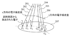
- FIG. 2A and 2B are diagrams illustrating a method of imaging the signal amount of electrons emitted from the semiconductor wafer 207 when the semiconductor wafer is scanned and irradiated with an electron beam.
- the electron beam is irradiated by scanning, for example, 201 to 203 or 204 to 206 in the x and y directions. It is possible to change the scanning direction by changing the deflection direction of the electron beam.
- FIG. 2A shows the positions on the semiconductor wafer irradiated with the electron beams 201 to 203 scanned in the x direction by G 1 to G 3 , respectively, and similarly irradiated with the electron beams 204 to 206 scanned in the y direction.
- the locations on the semiconductor wafer are indicated by G 4 to G 6 , respectively.
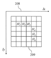
- the signal amount of the electrons emitted at the irradiation positions G 1 to G 6 becomes the five brightness values of the pixels H 1 to H 6 in the image 209 shown in FIG. 2B, respectively (lower right subscript 1 in G and H) ⁇ 6 correspond to each other).
- a coordinate system 208 indicates the x and y directions on the image.
- the computer system (processing / control unit) 115 performs processing for sending a control signal to the stage controller 119 and the deflection control unit 120 in order to capture an imaging point based on an imaging recipe, or any processing on the semiconductor wafer 101 Processing and control such as performing various image processing on the captured image at the imaging point is performed.
- imaging points are all of AP (Addressing Point), AFC (Auto Focus Point), AST (Auto Stigma Point), ABCC (Auto Brightness Contrast Point), and EP (Evaluation Point), or part of them. Is included.
- the computer system (processing / control unit) 115 is connected to the display 116 and includes a GUI (GraphicGraphUser Interface) that displays an image or the like to the user.
- GUI GraphicGraphUser Interface
- the XY stage 117 moves the semiconductor wafer 101 and enables image pickup at an arbitrary position on the semiconductor wafer.
- stage shift changing the observation position by the XY stage 117
- beam shift changing the observation position by deflecting the electron beam by the deflector 106
- the stage shift has a wide movable range but low imaging position positioning accuracy.
- the beam shift has a property that the movable range is narrow but the imaging position positioning accuracy is high.
- FIG. 1 shows an example in which two detectors for reflected electron images are provided, the number of detectors for reflected electron images can be reduced or increased.
- the computer system (processing / control unit) 115 described above generates an imaging recipe by a method described later, and controls the SEM device based on the imaging recipe to perform imaging, but part of these processes / controls. Alternatively, all of them can be assigned to a plurality of different processing terminals for processing / control. Details of the imaging sequence will be described later with reference to FIGS. 3A and 3B.
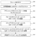
- FIG. 3A is a diagram illustrating a typical imaging sequence for observing an arbitrary EP. Imaging points, imaging order, and imaging conditions in the imaging sequence are specified by the imaging recipe.
- step 301 in FIG. 3A a semiconductor wafer as a sample is mounted on the stage 117 of the SEM apparatus.
- step 302 the global alignment mark on the wafer is observed with an optical microscope or the like, and the deviation of the wafer origin and the rotation of the wafer are corrected using the observation result.
- step 303 the processing / control unit 115 moves the stage 117 based on the imaging recipe, moves the imaging position to the AP, performs imaging, obtains an addressing parameter, and performs addressing using the obtained parameter.
- an AP to which a coordinate value of an imaging point and a template (imaging point pattern) are given in advance is used for positioning. Since the template is registered in the imaging recipe, it is hereinafter referred to as a registered template.
- the AP is selected from the vicinity of the EP (a range that can be moved by beam shift at the maximum).
- the AP since the AP generally has a low-magnification field of view with respect to the EP, there is a low risk that all the patterns to be imaged will be out of the field of view even if there is a slight shift in the imaging position. Therefore, by matching the registered template of the AP registered in advance with the SEM image (actual imaging template) of the AP actually captured, the positional deviation amount of the imaging point at the AP can be estimated.
- the relative displacement amount between AP and EP can be obtained, and the positional deviation amount of the imaging point at the AP can also be estimated by the aforementioned matching. For this reason, the relative displacement amount from the AP imaging position to be actually moved to the EP can be found by subtracting the displacement amount from the relative displacement amount between AP and EP. Therefore, the EP can be imaged with high coordinate accuracy by moving by the beam shift with high positioning accuracy by the relative displacement amount.
- the image template in the AP to be registered is registered once with a CAD data template, and the AP obtained at the time of actual imaging is registered. Variations such as re-registering an SEM image as an SEM image template are conceivable (see Patent Document 3).
- the electron beam normal incidence coordinate is set to the center coordinate of the EP, so the AP selection range is a beam shift movable range centered on the EP at the maximum, but the electron beam normal incidence coordinate is the center coordinate of the EP. If they are different, the beam shift movable range from the electron beam normal incidence coordinate becomes the selection range. Also, depending on the allowable electron beam incident angle required for the imaging point, the search range from the electron beam normal incidence coordinate may be smaller than the beam shift movable range. The same applies to the other templates.
- step 304 based on the imaging recipe, the processing / control unit 115 moves the imaging position to AF by beam shift to perform imaging, obtains autofocus adjustment parameters, and performs autofocus adjustment with the obtained parameters. Do.
- AF a description of AF is added.
- Auto-focusing is performed in order to acquire a clear image at the time of imaging, but if the sample is irradiated with an electron beam for a long time, contaminants adhere to the sample. Therefore, in order to suppress the adhesion of contamination in the EP, a measure is taken in which the coordinates around the EP are once observed as AF, an autofocus parameter is obtained, and then the EP is observed based on this parameter.
- the registered AF is a pattern that exists at a distance that can be moved by beam shift from (i) AP and EP, and the FOV at the time of AF imaging does not include the FOV at the time of EP imaging.
- the imaging magnification is about the same as the imaging magnification of EP (however, this is the case of AF for EP, and in the case of AF for AP, AF is imaged at an imaging magnification similar to the imaging magnification of the AP.
- AST and ABCC which will be described later
- step 305 the processing / control unit 115 moves the imaging position to the AST by beam shift to perform imaging, obtains an auto stigma adjustment parameter, and performs auto stigma adjustment using the obtained parameter.
- Astigmatism correction is performed in order to acquire an image without distortion at the time of imaging. Like AF, if a sample is irradiated with an electron beam for a long time, contaminants adhere to the sample. Therefore, in order to suppress the adhesion of contamination in EP, a measure is taken in which coordinates near the EP are once observed as AST, parameters for correcting astigmatism are obtained, and then EP is observed based on these parameters.
- the registered AST is (i) a pattern that exists at a distance that can be moved by beam shift from AP and EP, and the FOV at the time of AST imaging does not include the FOV at the time of EP imaging.
- AST The imaging magnification of the lens is equivalent to the imaging magnification of the EP, and (iii) has a pattern shape that facilitates astigmatism correction (is easy to detect image blur caused by astigmatism). It is desirable.
- step 306 the processing / control unit 115 moves the imaging position to ABCC by beam shift to perform imaging, obtains parameters for brightness / contrast adjustment, and performs auto brightness / contrast adjustment using the obtained parameters. I do.
- ABCC ABCC
- parameters such as a voltage value of a photomultiplier (photomultiplier tube) in the secondary electron detector 109, for example, an image signal
- the highest part and the lowest part are set so as to achieve full contrast or a contrast close thereto.
- AF when a sample is irradiated with an electron beam for a long time, contaminants adhere to the sample. Therefore, in order to suppress the adhesion of contamination in EP, a method is employed in which coordinates near the EP are once observed as ABCC, parameters for brightness / contrast adjustment are obtained, and then EP is observed based on these parameters.
- the registered ABCC is a pattern that exists at a distance that can be moved by beam shift from AP and EP, and the FOV at the time of ABCCC imaging does not include the FOV at the time of EP imaging, (ii)
- the imaging magnification of ABCC is about the same as the imaging magnification of EP. (Iii) Since the brightness and contrast of the image captured at the measurement point using the parameters adjusted in ABCC are good, ABCC It is desirable to satisfy the condition that the pattern is similar to the pattern in FIG.
- AP, AF, AST, and ABCC imaging in steps 303 to 306 described above may be partially or completely omitted depending on circumstances, the order of 303 to 306 may be arbitrarily changed, or AP, AF , AST, and ABCC coordinates may overlap (for example, autofocus and autostigma are performed at the same location), and various variations may be possible.
- the processing / control unit 115 moves the imaging point to EP by beam shift and performs imaging, for example, performs pattern length measurement under the set length measurement conditions.
- the EP matching between the captured SEM image and a registered template corresponding to the EP position registered in the imaging recipe in advance may be performed to detect the deviation of the measurement position.
- the imaging recipe information such as the coordinates of the imaging points (EP, AP, AF, AST, ABCC), the imaging sequence, and imaging conditions are written, and the SEM observes the EP based on the imaging recipe.
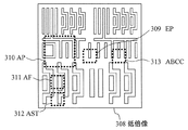
- FIG. 3B is a diagram illustrating an example of template positions of EP309, AP310, AF311, AST312, and ABCC313 on the low-magnification image 308 included in the imaging sequence. Each point is illustrated by a dotted frame.
- ⁇ About imaging recipe> When a wiring pattern is formed on a semiconductor wafer, a coating material called a resist is applied on the semiconductor wafer, and an exposure mask (reticle) for the wiring pattern is overlaid on the resist. Is used to form a wiring pattern by exposing the resist to light. Since the shape of the wiring pattern obtained in this way changes depending on the intensity of the visible light, ultraviolet light, or electron beam irradiated, and the aperture, it is necessary to inspect the pattern quality to form a highly accurate wiring pattern. is there.
- CD-SEM Critical Dimension Scanning Electron Microscope
- AP AFP
- ASP ASP
- ABCC ABCC
- the imaging position deviation amount in addressing is obtained by matching between an SEM image of an AP whose coordinates are known registered in advance as a registration template and an SEM image (actual imaging template) observed in an actual imaging sequence.
- the obtained deviation amount is estimated as the positional deviation amount.
- EP, AP, AFC, AST, and ABCC are collectively referred to as an imaging point, and the coordinates, size, and shape of points including part or all of the imaging point, imaging sequence, imaging conditions, and registered templates are managed as imaging recipes. Is done.
- CAD data Computer Aided Design
- imaging points AP, AFC, (AST and ABCC) (a1) number of points, (a2) coordinates, (a3) size and shape, (a4) imaging sequence (including imaging sequence of EP and imaging points, and electron beam normal incidence coordinates), (A5) Imaging position changing method (stage shift, beam shift), (a6) Imaging conditions (probe current, acceleration voltage, scanning direction of electron beam, etc.), (a7) Evaluation value or priority of imaging sequence or template
- the imaging recipe is generated so as to include some or all of the imaging parameters.
- the imaging recipe is preferably applied to a semiconductor inspection system that registers the above-described imaging parameters and a template such as an AP template.
- EP coordinates, size and shape, and imaging conditions As evaluation point information, and (b2) CAD data around EP (including layer information) as design pattern information, Pattern removal information of mask data, pattern line width information, type of wafer to be imaged, process, and material information of pattern and base, and (b3) imaging point (AP, AF, (AST, ABCC) search range, necessary condition of a selection element index value to be satisfied by an imaging point (given by a threshold value of the index value, etc.), selection element index priority (given by a weight between index values, etc.), Prohibited areas that must not be selected as imaging points, estimated amount of shape deviation between design pattern and actual pattern, and device conditions ( Stage shift range, stage shift / beam shift estimation error), and (b4) required positioning accuracy for each imaging point as required by the user, required image quality (focus adjustment, stigma adjustment, brightness / contrast adjustment, contamination requirements) And any required or all of the required imaging time and (b5) history information (such as information on imaging points that have succeeded or
- some values of the above-described output information (imaging parameters) (a1) to (a7) or default values / settable ranges are used as input information. I did it. That is, it has a function of recording any combination of parameters from (a1) to (a7) and (b1) to (b5) as input information and recording any combination of parameters from (a1) to (a7) as output information. .
- Patent Document 1 describes a case where the SEM operator manually gives the EP coordinates, size, imaging conditions, and the like, and has not yet reduced the work time of the SEM operator.
- the outline of the method for setting the EP (FOV for measurement) based on a predesignated device is as follows.
- an imaging recipe for observing an EP is generated based on a device selected in advance on CAD data.
- the imaging range (FOV) for observing the EP includes (a1) coordinates (position) of the evaluation point EP including all device shapes, (a2) the number of points, and (a3) size and shape. Automatically calculated and registered in the imaging recipe. Also, (b1) device configuration information (coordinates, connection information, graphic information) and contour line extraction parameters as length measurement point information, (b2) a default EP size as user requirement specifications, and (b3) optimum EP size An arbitrary combination of parameters such as whether or not the data is converted is input information, and an arbitrary combination of parameters (a1) to (a3) is output information.
- the following effects can be obtained.
- the electrical characteristics of high-pair devices and critical path sections that are required to be finished with high accuracy are verified, and there is no adhesion.
- it is finished in a shape close to the design data, it can contribute to early detection in the manufacturing process of defects that cause abnormal operation.
- it is possible to suppress the occurrence of contamination in EP without intervening the SEM operator, and a highly accurate imaging recipe can be generated in a short time.
- FIG. 4 is a diagram showing an overview of the entire procedure (example) of the imaging recipe generation process including the EP setting as described above.
- the input information includes evaluation device information 401 including an element name and a net number (wiring number) to be measured, CAD data 402, and various parameters 403 such as a contour extraction parameter.
- the output information includes EP coordinate / size information 410 and an imaging sequence 411.
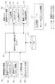
- the evaluation point automatic generation engine 404 sets an imaging point search range based on the input information (405), and subsequently executes EP coordinate / size and imaging sequence calculation (406).
- the processing 406 includes processing 407 for dividing the imaging points by the configuration graphic held in the database 412, EP coordinate optimization processing 408 for arranging the FOV for the configuration graphics, and imaging sequence optimization processing 409. And.
- the processing 408 for the FOV size optimization processing the size specified by the user may be used, or the FOV may be automatically determined based on the width of the wiring figure.
- EP coordinates / size, imaging sequence, input information, and output information are registered as an imaging recipe (413). Then, the image is actually captured based on the imaging recipe (414), and it is determined whether the obtained image is appropriate (415). If appropriate, the process ends. If not appropriate, the process is switched to another imaging point or imaging sequence and the imaging process is performed again (retry).
- FIG. 5 is a diagram showing input information and output information in the EP (FOV) arrangement processing.
- the reference numbers in FIG. 5 are different from those in FIG. 4, different reference numbers are used in the sense that they are specialized in EP placement processing.
- FIG. 6A to 6C are flowcharts for explaining details of the EP arrangement processing.
- FIG. 7 is a diagram illustrating a correspondence between circuit design data and layout design data in an evaluation device (example).
- 8 and 9 are diagrams illustrating a state in which an FOV is allocated.
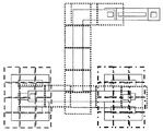
- FIG. 10 is a diagram illustrating a result of the EP placement process.
- FIG. 5 illustrates the information required for automatic evaluation point generation and the content of information output as a recipe.
- information 502 to 506 positioned at the end points of arrows (513 is a legend) extending to an evaluation point automatic generation engine (hereinafter also simply referred to as “engine”) 501 indicates that it is input information of the engine 501.
- engine 501 an evaluation point automatic generation engine
- information 507 to 512 located at the end points of links (514 is a legend) connected to the engine 501 by black circles indicate that the information can be input information and output information of the engine 501.
- the engine 501 can calculate and output any combination of information 502 to 506 and 507 to 512 as input information and any combination of information 507 to 512 as output information. It is characterized by being. Further, information in an arbitrary combination of information 502 to 506 and 507 to 512 can be excluded as unnecessary information from both input and output information.
- the first is a method in which a user specifies a fixed value of input information as input information, or a default value prepared in advance in the database 515 or the like is set as input information.
- the engine 501 calculates an arbitrary output value on the assumption of a fixed value or a default value.
- input information can be included in the output information. In this case, the engine 501 recalculates and outputs an appropriate value of the input information based on the input information.
- the second method is to set a range of values that can be taken by the user, or to set a default value of a range of values that can be taken by the input information prepared in advance in the database 515 or the like.
- the engine 501 calculates arbitrary output information on the assumption that the input information can change within this range. Also in this case, input information can be included in the output information. In that case, the engine 501 calculates and outputs an appropriate value of the input information within the range of values that the input information can take.
- Evaluation point information 502 includes evaluation device information [q] 503 and evaluation point parameter information 504.
- the shape of the evaluation point is generally a square region or a rectangular region, but other arbitrary shapes can be set as the imaging range.
- evaluation point information 508 coordinates 509 of evaluation point EP [p], evaluation point EP [p] size 510, EP [p] combined label 511, imaging sequence (imaging Order, etc.) 512.
- the imaging sequence 512 is for designating in what order the EP [p] is imaged or how various processes are performed.
- the database 515 stores and manages a part or all of the information 502 to 512 described above.
- the aforementioned information can be handled as common information as information across time series or between different SEM devices.
- the evaluation point automatic generation engine 501 can read arbitrary information from the database 515 as necessary and reflect it in various processes. Further, when determining the values or ranges of the various input information 502 to 512, it is possible to refer to past parameters stored in the database 515, and for example, various input information values or range defaults for each type and manufacturing process. It is possible to save the value.
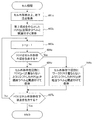
- FIGS. 6A to 6C are flowcharts for explaining the details of the entire evaluation point automatic generation processing.
- the engine 501 acquires from CAD data an evaluation device [Nq] that is automatically specified by a user or automatically specified by critical path information by hot spot extraction or timing analysis. Examples of measurement devices specified on CAD data are shown in FIGS. 7A and 7B.
- FIG. 7A shows an example of the evaluation device specified on the circuit design data even in the CAD data
- FIG. 7B shows an example of the evaluation device specified on the layout design data in the CAD data.
- the circuit design data and the layout design data are related and can be collated (LVS: LayoutSVersus Schematic). Therefore, by collating the critical path extracted by the timing analysis with the layout design data, it is possible to identify the device that needs to be evaluated on the actual device, and the measurement result on the actual device is used as the circuit design data. It is possible to analyze the electrical characteristics and timing by feeding back. That is, it is possible to identify which part corresponds to the wiring on the layout design data.
- step 602a the engine 501 initializes the evaluation point ID [p] and the evaluation device ID [q].
- step 603a the engine 501 takes in the graphic information of the evaluation device [q] serving as the base point from the CAD data. Note that evaluation points of all evaluation devices are generated through steps 603a to 609a.
- step 604a the engine 501 determines an EP-FOV magnification to be applied to the evaluation device [q].
- This magnification can be calculated from the minimum figure of the evaluation device constituent figure (for example, a square having sides of k times the width of the minimum constituent figure is FOV) or can be designated in advance by the user for each device. is there.
- step 605a the engine 501 checks the device type of the evaluation device [q] based on the CAD data, and branches the process depending on whether it is a wiring or a cell.
- the engine 501 When the evaluation device [q] is a wiring, the engine 501 performs processing of steps 601b to 612b (FIG. 6B) (details will be described later), and in the case of a cell, the engine 501 performs the processing of steps 601c to 607c (FIG. 6C). Processing (details will be described later) is performed.
- step 606a When the wiring process (step 606a) or the cell process (step 607a) is completed, in steps 608a and 609a, the engine 501 determines whether there is an evaluation device to be processed next. If there is, the process returns to step 603a. The process ends.
- FIG. 6B is a flowchart for explaining details of the wiring process (step 606a).
- the engine 501 acquires the constituent wiring element (graphic) [Nr] of the evaluation device [q]. This is because the wiring device is registered as one line segment information for each branch as indicated by 801 and 802 in FIG. 8 on the CAD data.
- step 602b the engine 501 initializes the wiring element ID [r].
- step 603b the engine 501 acquires vertex information [Ns] of the wiring element [r]. For example, as shown in FIG. 8, information about the vertex “•” is acquired.
- step 603b to step 612b evaluation points including all the wiring elements are generated.
- step 604b the engine 501 initializes the vertex number ID [s] for the vertex acquired in step 603b.
- step 605b the engine 501 stores the EP-FOV centered on the vertex [s] serving as the base point at the evaluation point [p] with a label that can be combined later.
- FIG. 8 shows an example of an EP-FOV arrangement example 803 and a label 804. In the example of FIG. 8, the upper right vertex is set as the start point.
- the engine 501 increments the vertex number ID [s] in step 606b, and increments the evaluation point [p] in step 607b. Thereby, the engine 501 determines in which direction the next vertex exists (determination of the vertex direction).
- Step 608b the engine 501 repeats Step 606b to Step 610b until it processes all the vertices of the wiring element [r].
- step 609b the engine 501 determines whether the vertex [s] (next vertex) is included in the EP-FOV (if the next vertex is included in the FOV, the arrangement direction is changed). If not included, as in the example of 805 in FIG. 8, in step 610b, EP-FOV [p] shifted in the vertex [s] direction so as not to overlap with EP-FOV [p-1] Is associated with (and appended to) a label that can be combined later.
- steps 603b to 610b is executed for all the wiring elements (configuration figures) (steps 611b and 612b).
- FIG. 6C is a flowchart for explaining the details of the cell processing.
- the engine 501 acquires the upper left and lower right vertex coordinates of the cell outline frame of the evaluation device [q], and determines the FOV placement direction.
- the arrangement direction is from left to right.
- step 602c the engine 501 stores the EP-FOV centered on the upper left vertex as the base point in association with a label that can be combined later (with a label added).
- FIG. 9 shows an EP-FOV arrangement 901 (example) and a label 902 (example).
- step 603c the engine 501 increments the evaluation point [p]. Then, evaluation points including all cell regions are generated through steps 604c to 607c.
- step 604c the engine 501 determines whether the EP-FOV includes the right side of the cell outline. If not included, the process proceeds to step 605c, and if included, the process proceeds to step 606c.
- step 605c the engine 501 can place the shifted EP-FOV on the right side of the cell outline so that the EP-FOVs do not overlap each other as shown in the FOV_X direction shift 903 in FIG. Associate (add a label) with the correct label and save.
- step 606c the engine 501 can place the shifted EP-FOV on the lower side of the cell outline so that the EP-FOVs do not overlap each other as shown in the FOV_Y direction shift 904 in FIG. Associate (add a label) with the correct label and save.
- the work FOV is the FOV that is first arranged in a row and is the reference FOV for arranging another FOV. In the example of FIG. 9, it is the leftmost FOV. That is, FOV_Q1-1 is a work FOV until FOV_Q2-1 in the next column is determined.
- step 607c the engine 501 determines whether the EP-FOV includes the cell outline frame lower right vertex, and repeats the processing from step 603c to step 607c until it includes.
- FIG. 10 is a diagram illustrating a state after the FOV is placed. As shown in FIG. 10, if the FOV placement processing according to the present invention is executed, the FOV can be appropriately placed according to the wiring and the cell, and the area where the FOVs overlap each other can be minimized. Become.
- the FOV is arranged along the device shape so that all the constituent areas necessary for the measurement of electrical characteristics can be accommodated in the FOV.
- the image acquisition conditions for arranging the images so as not to overlap are determined. As a result, it is not necessary for the user to manually input a portion having electrical characteristics, and a portion to be verified for circuit operation can be easily extracted.
- the wiring part of the device is represented by a combination of a plurality of basic constituent figures depending on the shape of the wiring part
- a process of arranging an FOV for each constituent figure is executed.
- the FOV is arranged with reference to the cell outer frame and the vertex.
- one of the vertices becomes the start point of the FOV placement process, and another vertex becomes the end point of the process.
- the measurement required part is represented by a combination of basic figures (a plurality of basic constituent figures are stored in the database). It becomes possible to arrange the FOV very easily. Therefore, the time for generating the evaluation points can be shortened, and the throughput of the recipe generation process can be increased.
- the wiring portion and the cell portion in the evaluation device are specified by collating (LVS) circuit design data and layout design data included in the CAD data.
- LVS collating
- a label indicating the imaging order is given to the FOV arranged in the portion to be measured on the evaluation device. This makes it possible to clarify the imaging sequence.
- the FOV arrangement state obtained as a result of the evaluation point (FOV) arrangement process is displayed on the display unit, the user can easily visually understand where to be measured. .
Landscapes
- Chemical & Material Sciences (AREA)
- Analytical Chemistry (AREA)
- Testing Or Measuring Of Semiconductors Or The Like (AREA)
- Length-Measuring Devices Using Wave Or Particle Radiation (AREA)
Abstract
FOV(Field Of View)を効率良く設定できる走査型電子顕微鏡装置を提供する。CADデータが有するデバイス形状情報(回路設計データとレイアウト設計データを含む)を用いて、電気特性測定の対象となる全ての要素が含まれるように、複数のFOVを少ない重なり量で配置する。デバイスの配線部分については、該配線部分を構成する複数の基本構成図形ごとに前記FOVを配置する。デバイスのセル部分については、セル外形枠とセル頂点を基準に前記FOVを配置する。
Description
本発明は、走査型電子顕微鏡(Scanning Electron Microscope)を用いた半導体デバイスの仕上がり形状測定を行うレシピ、特に評価ポイントの生成に関するものである。
半導体ウェーハにデバイス、又は配線パターンを形成する際には、半導体ウェーハ上にレジストと呼ばれる塗布材を塗布し、レジストの上にパターン形状の露光用マスク(レチクル)を重ね、その上から可視光線・紫外線などを露光し、レジストを感光することによってパターンを形成する方法が採用されている。このようにして得られたパターンは、照射する電子線の強度や絞りによってパターンの形状が変化するため、高精度のパターンを形成するにはパターンの出来栄えを検査する必要がある。
このようなパターンの検査には、測長走査型電子顕微鏡(Critical Dimension Scanning Electron Microscope:CD-SEM)が広く用いられている。CD-SEMによるパターン検査では、検査を要する半導体パターン上の任意の評価ポイントをCD-SEMによって観察し、その観察画像からパターンの幅の寸法や形状データを取得してパターンの出来栄えを評価している。
ところで、CD-SEMによってウェーハ上のパターンを撮像してパターン形状の評価を行うためには、評価ポイントの位置、倍率、及び画質を指定するレシピを作成する必要がある。従来、レシピはCD-SEM上にて作成されていたが、近年の半導体の高集積化に伴う評価ポイントの大幅な増加により、最近ではCADデータよりレシピを自動生成する手法が主流となりつつある。
また、近年の最先端半導体においては、プロセスルールが露光光源の波長よりも微細な寸法に到達している。このため、ウェーハへのパターン転写時に近接したパターンの光がOPE(Optical Proximity Effect)とよばれる現象により互いに干渉し、レチクルのパターンと異なるパターンがレジスト上に転写されてしまうことが問題となっている。この現象を回避するため、マスクに微細な補正用パターンを付加することにより転写するパターンの補正を行うOPC(Optical Proximity Correction)が一般的に用いられている。レイアウトパターンに対して付加されたOPCパターンによる補正効果の検証は主にリソシミュレータなどによって行うが、ウェーハへの転写時に形状が大きく異なる危険部位をHotSpotとして自動抽出し、抽出したHotSpotからレシピを自動生成し、実際のウェーハ上のパターンを測定して、仕上がり形状の厳密な検証を行っている。
また、最新のリソグラフィーでは、より強いOPC(パターンの変形度合いを強くすること)として、いわゆるアグレッシブOPC(より多くのOPCパターンを用いる)を採用する動きになっている。このアグレッシブOPCを採用するためには、従来のルールベースOPCでのデータの流れとは異なるデータの流れが必要になる。そこで、期待されているのがContourデータと言われる輪郭線データである。輪郭線データにより、従来のHotspot測定点だけではなく、形状の評価が可能となり、より高精度な検証を行うことができる(例えば、特許文献1参照)。
しかしながら、高いペア性が要求される(許容されるマージンが少ない)トランジスタやタイミング精度が極めて高い回路上のクリティカルパスについては、CADデータと同等に見えるレベルの仕上がり形状であっても、極微細な形状変化による特性変動において半導体動作に影響を及ぼす懸念がある。従って、これらについては仕上がり形状の相違からのHotSpotの自動抽出は困難であるとともに、仕上がり形状のみの検証では回路動作への影響の有無は判別できない。この場合、検証は回路特性シミュレーションによって行う必要がある。そのためには、電気特性のシミュレーションを行うことが可能なデバイス単位の形状を網羅して撮像し、つなぎ合わせるためのレシピが必要である。
ところが、特許文献1に記載の撮像レシピの自動生成によれば、HotSpot(MP点)を測定するための効果を発揮する(1点1点を正確に測定するためのレシピを作成する上では効果を発揮する)が、電気特性を持つデバイスの全ての箇所を撮像し、それぞれのFOVで撮像した部分画像を結合可能な状態とする提案はなされていない。
一方、チップ全面に対して仕上がり形状を撮像し、結合することでも前述の課題を解決することは可能であるが、測定に要する所要時間から考慮して現実的ではない。また、それら電気的特性などの危険部位の情報は製造段階ではなく、設計段階にて判明する部分であり、測定部位の指定は上流の設計者によって可能であるが、それらの情報を半導体検査側に渡すための有用な手段がなかった。つまり、設計情報上の位置がパターンレイアウト情報上の位置に対応するものではなく、一旦設計情報をパターンにすると、パターン上のある部分が配線なのかただの穴部や溝なのかパターンのみから判断するのは非常に困難である。
本発明はこのような状況に鑑みてなされたものであり、回路動作上要求される仕上がり精度検証のため、電気特性をもつデバイスを包含するFOV(即ち、評価ポイント(EP))の配置すべき位置を容易に決定するための画像取得条件決定技術を提供するものである。
上記課題を解決するため、本発明では、CADデータが有しているデバイス形状情報(回路設計データとレイアウト設計データを含む)から、電気特性測定に必要な構成領域を全てFOV内に収まるように、デバイス形状に沿ってFOVを重ならないように配置するための画像取得条件を決定する。なお、デバイスの配線部分については、配線部分の形状によっては複数の基本構成図形の組み合わせで表わされるので、各構成図形に対してFOVを配置する処理が実行される。セル部分については、セル外形枠と頂点を基準にFOVが配置される。その際、何れかの頂点がFOV配置処理の開始点となり、別の頂点が同処理の終点となる。
即ち、本発明は、評価デバイス上の評価ポイントに電子線を照射して、前記評価ポイントの画像を取得する走査型電子顕微鏡装置であり、評価デバイスのCADデータを入力する入力部と、CADデータに基づいて評価デバイスの評価ポイントを決定する評価ポイント生成部(評価ポイント自動生成エンジン)と、評価ポイント生成部によって決定された評価ポイントの情報を出力する出力部と、を備えている。評価ポイント生成部は、評価デバイス上の配線部分及びセル部分を、CADデータに基づいて特定し、当該特定部分に対して評価ポイントに相当するFOV(Field Of View)決定し、当該決定されたFOVを特定部分に配置する。配線部分及びセル部分の特定は、CADデータに含まれる回路設計データとレイアウト設計データとを照合することにより行われる。配置したFOVに対しては、撮像順序を示すラベルが付与される。
当該走査型電子顕微鏡は、さらに、デバイスを構成する複数種類の基本構成図形を格納する基本構成図形データベースを備えている。この場合、評価ポイント生成部は、基本構成図形データベースを参照して、レイアウト設計データが有する基本構成図形を抽出し、配線部分については、当該配線部分を構成する基本構成図形の複数の頂点を特定する。そして、評価ポイント生成部は、基本構成図形においてFOVの配置を開始する第1の頂点とFOVの配置を終了する第2の頂点を決定し、第1の頂点(開始点)から第2の頂点(終了点)の方向に前記FOVを、互いのFOVの重なる面積が最小となるように配置する。なお、配線部分が複数の基本構成図形によって構成される場合、評価ポイント生成部は、基本構成図形毎に前記第1及び第2の頂点を決定し、FOVを配置する。
また、評価ポイント生成部は、セル部分については、セル外形からFOV配置始点となる開始頂点とFOV配置終点となる終了頂点を特定し、開始頂点から終了頂点に向けて順番にFOVを、互いのFOVが重ならないように配置する。
さらなる本発明の特徴は、以下本発明を実施するための最良の形態および添付図面によって明らかになるものである。
本発明によれば、電気的特性を持つデバイス部位を全て撮像するためのFOVを効率よく設定することが可能となり、結果として、高精度な測定を効率よく実現することが可能となる。
本発明は、レイアウト設計情報からだけではどこに電気特性を持つか不明なデバイスについて、電気特性を持つ部位を特定し、その部位にFOVを効率よく(できるだけ重複部分が生じないように)配置する技術に関するものである。例えば、本発明では、EDA(Electronic Design Automation)ツールを用いて作成した半導体設計データが有するデバイス構成情報や接続情報を使用することにより、電気的特性検証に必要な半導体デバイス上のパターンを包含するレシピ(評価ポイント)を自動生成する。
以下、添付図面を参照して本発明の実施形態について説明する。ただし、本実施形態は本発明を実現するための一例に過ぎず、本発明の技術的範囲を限定するものではないことに注意すべきである。
<走査型電子顕微鏡の構成>
図1は、本発明の実施形態による、試料の二次電子像(Secondary Electron:SE像)あるいは反射電子像(Backscattered Electron:BSE像)を取得する走査型電子顕微鏡(Scanning Electron Microscope:SEM)の概略構成を示すブロック図である。なお、ここでは、SE像とBSE像を総称してSEM画像と呼ぶこととする。また、ここで取得される画像は、測定対象を垂直方向から観察したトップダウン画像、あるいは任意の傾斜角方向から観察したチルト画像の一部または全てを含むものとする。
図1は、本発明の実施形態による、試料の二次電子像(Secondary Electron:SE像)あるいは反射電子像(Backscattered Electron:BSE像)を取得する走査型電子顕微鏡(Scanning Electron Microscope:SEM)の概略構成を示すブロック図である。なお、ここでは、SE像とBSE像を総称してSEM画像と呼ぶこととする。また、ここで取得される画像は、測定対象を垂直方向から観察したトップダウン画像、あるいは任意の傾斜角方向から観察したチルト画像の一部または全てを含むものとする。
図1において、103は電子銃であり、電子ビーム104を発生する。ステージ117上に置かれた試料である半導体ウェーハ101上の任意の位置において、電子線が焦点を結んで照射されるように、偏向器106および対物レンズ108により電子線の照射位置と絞りが制御される。
電子線を照射された半導体ウェーハ101からは、二次電子と反射電子が放出され、E×B偏向器107によって照射電子線の軌道と分離された二次電子は109の二次電子検出器により検出される。一方、反射電子は反射電子検出器110及び111により検出される。反射電子検出器110及び111は互いに異なる方向に設置されている。二次電子検出器109と反射電子検出器110及び111によって検出された二次電子及び反射電子は、A/D変換機112乃至114によってデジタル信号に変換され、画像データとして画像メモリ122に格納される。その後、CPU121は、画像メモリ122に格納されている画像データに対して、目的に応じた画像処理を実行する。
図2A、2Bは、半導体ウェーハ上に電子線を走査して照射した際、半導体ウェーハ207上から放出される電子の信号量を画像化する方法を示す図である。図2Aに示すように、電子線は、例えばx、y方向に201~203又は204~206のように走査して照射される。電子線の偏向方向を変更することによって走査方向を変化させることが可能である。図2Aは、x方向に走査された電子線201~203が照射された半導体ウェーハ上の場所をそれぞれG1~G3で示し、同様にy方向に走査された電子線204~206が照射された半導体ウェーハ上の場所をそれぞれG4~G6で示している。照射位置G1~G6において放出された電子の信号量は、それぞれ図2B内に示した画像209における画素H1~H6の明度5値になる(G、Hにおける右下の添え字1~6は互いに対応する)。208は画像上のx、y方向を示す座標系である。
図1に戻り、説明を続ける。コンピュータシステム(処理・制御部)115は、撮像レシピを基に撮像ポイントを撮像するために、ステージコントローラ119や偏向制御部120に対して制御信号を送る処理、あるいは、半導体ウェーハ101上の任意の撮像ポイントにおける撮像画像に対し各種画像処理を行う等の処理・制御を行う。ここで撮像ポイントとは、AP(Addressing Point)、AFC(Auto Focus Point)、AST(Auto Stigma Point)、ABCC(Auto Brightness Contrast Point)、及びEP(Evaluation Point)の全て、又はそれらの一部を含むものである。また、コンピュータシステム(処理・制御部)115は、ディスプレイ116と接続されており、ユーザに対して画像等を表示するGUI(Graphic User Interface)を備えている。
XYステージ117は、半導体ウェーハ101を移動させ、半導体ウェーハ上の任意の位置での画像撮像を可能にしている。ここでは、XYステージ117により観察位置を変更することをステージシフト、偏向器106により電子線を偏向することにより観察位置を変更することをビームシフトと呼ぶこととする。一般に、ステージシフトは、可動範囲は広いが撮像位置の位置決め精度が低く、逆にビームシフトは、可動範囲は狭いが撮像位置の位置決め精度が高いという性質がある。
なお、図1では反射電子像の検出器を2つ備えた例を示したが、反射電子像の検出器の数を減らすこともあるいは増やすことも可能である。
また、前述したコンピュータシステム(処理・制御部)115は、後述する方法により撮像レシピを生成し、また撮像レシピに基づいてSEM装置を制御して撮像を行うが、これらの処理・制御の一部又は全てを異なる複数台の処理端末に割り振って処理・制御することも可能である。撮像シーケンスの詳細については、図3A、3Bを用いて後述する。
図1に示される走査型電子顕微鏡装置を用いて測定対象を任意の傾斜角方向から観察したチルト画像を得る方法としては、(i)電子光学系より照射する電子線を偏向し、電子線の照射角度を傾斜させて傾斜画像を撮像する方式(例えば、特許文献2参照)、(ii)半導体ウェーハを移動させるステージ117自体を傾斜させる方式(図1においてはチルト角118でステージが傾斜している)、及び(iii)電子光学系自体を機械的に傾斜させる方式等がある。
<SEM撮像シーケンスについて>
図3Aは、任意のEPを観察するための代表的な撮像シーケンスを示す図である。撮像シーケンスにおける撮像ポイント・撮像順序・撮像条件は、撮像レシピにより指定される。
図3Aは、任意のEPを観察するための代表的な撮像シーケンスを示す図である。撮像シーケンスにおける撮像ポイント・撮像順序・撮像条件は、撮像レシピにより指定される。
まず、図3Aのステップ301では、試料である半導体ウェーハがSEM装置のステージ117上に取り付けられる。また、ステップ302では、光学顕微鏡等でウェーハ上のグローバルアライメントマークを観察し、その観察結果を用いてウェーハの原点ずれやウェーハの回転が補正される。
ステップ303では、処理・制御部115が、撮像レシピに基づいてステージ117を移動させ、撮像位置をAPに移動して撮像し、アドレッシングのパラメータを求め、求められたパラメータによってアドレッシングを行う。
ここで、APについて説明を加えておく。EPを観察する場合、ステージシフトにより直接EPを観察しようとするとステージの位置決め精度により大きく撮像ポイントがずれてしまう危険性がある。そこで、いったん位置決め用としてあらかじめ撮像ポイントの座標値とテンプレート(撮像ポイントのパターン)が与えられたAPを観察する。テンプレートは撮像レシピに登録されるので、以降登録テンプレートと呼ぶ。APはEPの近傍(最大でもビームシフトにより移動可能な範囲)から選択される。また、APはEPに対して一般に低倍視野であるため、多少の撮像位置のずれに対しても撮像したいパターンがすべて視野外になる危険性は低い。そこで、あらかじめ登録されたAPの登録テンプレートと実際に撮像されたAPのSEM像(実撮像テンプレート)をマッチングすることにより、APにおける撮像ポイントの位置ずれ量を推定することができる。
AP及びEPの座標値は既知なのでAP-EP間の相対変位量を求めることができ、かつAPにおける撮像ポイントの位置ずれ量も前述のマッチングにより推定できる。このため、AP-EP間の相対変位量から位置ずれ量を差し引くことにより実際に移動すべきAP撮像位置からEPまでの相対変位量が分かる。よって、相対変位量分だけ位置決め精度の高いビームシフトによって移動することにより高い座標精度でEPを撮像することが可能となる。
これを可能にするためには、登録されるAPは(i)EPからビームシフトにより移動可能な距離に存在するパターンであり(かつEPにおけるコンタミネーションの発生を抑えるためAP撮像時の範囲(Field of View:FOV=EP)にEP撮像時のFOVを含まないことを条件とする場合もある)、(ii)APの撮像倍率はステージの位置決め精度を加味してEPの撮像倍率よりも低く、(iii)パターン形状あるいは明度パターンが特徴的であり、登録テンプレートと実撮像テンプレートとのマッチングがし易い等の条件を満たしていることが望ましい。どの場所をAPとして選択するかに関しては、従来SEMオペレータが手動で行っていたが、自動で良好なAPの選択および撮像シーケンスの決定を行うことを特徴とする。
登録するAPにおける画像テンプレートは、CAD画像、SEM画像、或いは画像テンプレートの登録のためだけに撮像を行うのを避けるために、一旦CADデータテンプレートで登録しておき、実際の撮像時に得たAPのSEM画像をSEM画像テンプレートとして再登録する等のバリエーションが考えられる(特許文献3参照)。
なお、前述のAP選択範囲について補足する。一般的に電子ビーム垂直入射座標はEPの中心座標に設定されるため、APの選択範囲は最大でもEPを中心としたビームシフト可動範囲としたが、電子ビーム垂直入射座標がEPの中心座標と異なる場合は電子ビーム垂直入射座標からのビームシフト可動範囲が選択範囲となる。また撮像ポイントに要求される許容電子ビーム入射角によっては、電子ビーム垂直入射座標からの探索範囲もビームシフト可動範囲より小さくなることがある。これらは他のテンプレートについても同様である。
図3Aに戻り説明を続ける。ステップ304では、処理・制御部115が、撮像レシピに基づいて、ビームシフトにより撮像位置をAFに移動して撮像し、オートフォーカス調整のパラメータを求めて、求められたパラメータにてオートフォーカス調整を行う。
ここで、AFについて説明を加えておく。撮像時には鮮明な画像を取得するためオートフォーカスを行うが、試料に電子線を長く照射すると汚染物質が試料に付着してしまう。そこで、EPにおけるコンタミネーションの付着を抑えるため、いったんEP周辺の座標をAFとして観察し、オートフォーカスのパラメータを求めてからこのパラメータを基にEPを観察するという手段が採られる。
そのため、登録されるAFは(i)AP、EPからビームシフトにより移動可能な距離に存在するパターンであり、かつAF撮像時のFOVにEP撮像時のFOVは含まれない、(ii)AFの撮像倍率はEPの撮像倍率と同程度である(ただし、これはEP用のAFの場合であり、AP用のAFの場合は前記APの撮像倍率と同程度の撮像倍率でAFを撮像する。後述するAST、ABCCに関しても同様)、(iii)オートフォーカスをかけやすいパターン形状をもつ(フォーカスずれに起因する像のボケを検出し易い)等の条件を満たしていることが望ましい。
次にステップ305では、処理・制御部115がビームシフトにより撮像位置をASTに移動して撮像し、オートスティグマ調整のパラメータを求めて、求められたパラメータに用いてオートスティグマ調整を行う。
ここでASTについて説明を加えておく。撮像時には歪みのない画像を取得するため非点収差補正を行うが、AFと同様、試料に電子線を長く照射すると汚染物質が試料に付着してしまう。そこで、EPにおけるコンタミネーションの付着を抑えるため、いったんEP近くの座標をASTとして観察し、非点収差補正のパラメータを求めてから、このパラメータを基にEPを観察するという手段が採られる。
そのため登録されるASTは、(i)AP及びEPからビームシフトにより移動可能な距離に存在するパターンであり、かつ、AST撮像時のFOVにEP撮像時のFOVは含まれない、(ii)ASTの撮像倍率はEPの撮像倍率と同程度である、(iii)非点収差補正をかけ易いパターン形状を持つ(非点収差に起因する像のぼけを検出し易い)等の条件を満たしていることが望ましい。
続いて、ステップ306では、処理・制御部115が、ビームシフトにより撮像位置をABCCに移動して撮像し、ブライトネス・コントラスト調整のパラメータを求めて、求められたパラメータを用いてオートブライトネス・コントラスト調整を行う。
ここでABCCについて説明を加えておく。撮像時には適切な明度値及びコントラストをもつ鮮明な画像を取得するために、例えば二次電子検出器109におけるフォトマル(光電子増倍管)の電圧値等のパラメータを調整することによって、例えば画像信号の最も高い部分と最も低い部分とがフルコントラストあるいはそれに近いコントラストになるように設定する。しかし、AFと同様試料に電子線を長く照射すると汚染物質が試料に付着してしまう。そこで、EPにおけるコンタミネーションの付着を抑えるため、いったんEP近くの座標をABCCとして観察し、ブライトネス・コントラスト調整のパラメータを求めてからこのパラメータを基にEPを観察するという方法が採られている。
そのため、登録されるABCCは、(i)AP、EPからビームシフトにより移動可能な距離に存在するパターンであり、かつ、ABCC撮像時のFOVにEP撮像時のFOVは含まれない、(ii)ABCCの撮像倍率はEPの撮像倍率と同程度である、(iii)ABCCにおいて調整したパラメータを用いて測長ポイントにおいて撮像した画像のブライトネスやコントラストが良好であるために、ABCCは前記測長ポイントにおけるパターンに類似したパターンである等の条件を満たしていることが望ましい。
なお、前述したステップ303乃至306におけるAP、AF、AST、及びABCCの撮像は、場合によっては一部あるいは全てが省略されたり、303乃至306の順番が任意に入れ替えられたり、或いは、AP、AF、AST、及びABCCの座標で重複するものがあったり(例えばオートフォーカス、オートスティグマを同一箇所で行う)等、様々なバリエーションがありうるものである。
最後に、ステップ307では、処理・制御部115が、ビームシフトにより撮像ポイントをEPに移動して撮像し、例えば設定した測長条件でパターンの測長等を行う。EPにおいても撮像したSEM画像と事前に撮像レシピに登録されたEP位置に対応する登録テンプレートなどでマッチングを行い計測位置のずれを検出することがある。撮像レシピには前述の撮像ポイント(EP、AP、AF、AST、ABCC)の座標や撮像シーケンス、撮像条件などの情報が書き込まれておりSEMは前記撮像レシピに基づいてEPを観察する。
図3Bは、撮像シーケンスに含まれる、低倍像308上のEP309、AP310、AF311、AST312、及びABCC313のテンプレート位置の一例を示す図である。各ポイントは点線枠で図示されている。
<撮像レシピについて>
半導体ウェーハに配線パターンを形成する際は、半導体ウェーハ上にレジストと呼ばれる塗布材を塗布し、レジストの上に配線パターンの露光用マスク(レチクル)を重ね、その上から可視光線・紫外線あるいは電子ビームを照射し、レジストを感光することによって配線パターンを形成する方法が採用されている。このようにして得られた配線パターンは照射する可視光線・紫外線あるいは電子ビームの強度や絞りによってパターンの形状が変化するため、高精度の配線パターンを形成するにはパターンの出来栄えを検査する必要がある。
半導体ウェーハに配線パターンを形成する際は、半導体ウェーハ上にレジストと呼ばれる塗布材を塗布し、レジストの上に配線パターンの露光用マスク(レチクル)を重ね、その上から可視光線・紫外線あるいは電子ビームを照射し、レジストを感光することによって配線パターンを形成する方法が採用されている。このようにして得られた配線パターンは照射する可視光線・紫外線あるいは電子ビームの強度や絞りによってパターンの形状が変化するため、高精度の配線パターンを形成するにはパターンの出来栄えを検査する必要がある。
この測定には、測長走査型電子顕微鏡(Critical Dimension Scanning Electron Microscope:CD-SEM)が広く用いられている。測定を要する半導体パターン上の危険ポイントを評価ポイント(以降EPと呼ぶ)としてSEMにて観察しその観察画像からパターンの配線幅などの各種寸法値を計測し、これらの寸法値からパターンの出来栄えを評価している。
EPを位置ずれなく、かつ高画質で撮像するため、上述したように、AP、AFP、ASP、あるいはABCCの一部または、全てを撮像ポイントとして設定し、それぞれの撮像ポイントにおいてアドレッシング、オートフォーカス調整、オートスティグマ調整、及びオートブライトネス・コントラスト調整を行っている。
アドレッシングにおける撮像位置ずれ量は、事前に登録テンプレートとして登録された座標既知のAPにおけるSEM画像と、実際の撮像シーケンスにおいて観察されたSEM画像(実撮像テンプレート)にてマッチングを行い、このマッチングによって得られたずれ量を位置ずれ量として推定している。EP、AP、AFC、AST、ABCCをまとめて撮像ポイントと呼び、撮像ポイントの一部または全てを含むポイントの座標・サイズ・形状と、撮像シーケンス・撮像条件と、登録テンプレートは、撮像レシピとして管理される。
従来、撮像レシピの生成はSEMオペレータが手動で行っており、多大な労力と時間を要する作業であった。また、各撮像ポイントの決定や登録テンプレートを撮像レシピに登録するためには、実際にウェーハを低倍で撮像する必要があることから、撮像レシピの生成がSEMの稼働率低下の一因となっていた。更に、パターンの微細化に伴うOPC(Optical Proximity Correction)技術等の導入により、評価を要するEPの点数は爆発的に増加している。そのため、撮像レシピをマニュアルで生成することは非現実的になりつつある。
そこで、低倍視野でのウェーハ上のパターンの設計情報である半導体の回路設計データ(以降CADデータ(Computer Aided Design)と呼ぶ)を基づいて、EPを観察するための撮像ポイント(AP、AFC、AST、及びABCC)の(a1)点数と、(a2)座標と、(a3)サイズ・形状と、(a4)撮像シーケンス(EPや撮像ポイントの撮像順序、電子ビーム垂直入射座標を含む)と、(a5)撮像位置変更方法(ステージシフト、ビームシフト)と、(a6)撮像条件(プローブ電流、加速電圧、電子ビームのスキャン方向など)と、(a7)撮像シーケンスあるいはテンプレートの評価値あるいは優先順位の、一部又は全ての撮像パラメータを含むように撮像レシピを生成する。さらに、撮像レシピは、上述の撮像パラメータと、APテンプレートなどのテンプレートを登録する半導体検査システムに適用されることが望ましい。
撮像レシピ生成のための入力情報としては、(b1)評価ポイント情報としてEPの座標、サイズ・形状、及び撮像条件と、(b2)設計パターン情報としてEP周辺のCADデータ(レイヤー情報を含む)、マスクデータのパターン抜き残し情報、パターンの線幅情報、撮像するウェーハの品種、工程、及びパターンや下地の材質情報と、(b3)撮像レシピ自動生成エンジンの処理パラメータとして撮像ポイント(AP、AF、AST、ABCC)の探索範囲、撮像ポイントが満たすべき選択要素指標値の必要条件(指標値のしきい値などで与えられる)、選択要素指標優先順位(指標値間の重みなどで与えられる)、撮像ポイントとして選択してはならない禁止領域、設計パターンと実パターンとの形状乖離推定量、及び装置条件(ステージシフト範囲、ステージシフト/ビームシフト推定誤差)と、(b4)ユーザ要求仕様として各撮像ポイントに対する撮像位置の要求位置決め精度、要求画質(フォーカス調整、スティグマ調整、ブライトネス・コントラスト調整、コンタミネーションに関する要求やEPにおける許容電子ビーム入射角に関する要求を含む)、及び要求撮像時間と、(b5)履歴情報(過去に成功したまたは失敗した撮像ポイントの情報など)の、何れか又は全てを含むようにすると良い。
更に、前述の入力情報(b1)乃至(b5)に加えて、前述した出力情報(撮像パラメータ)(a1)乃至(a7)の一部の値あるいは、デフォルト値・設定可能範囲を入力情報とするようにした。すなわち、(a1)乃至(a7)および(b1)乃至(b5)から任意のパラメータの組み合わせを入力情報とし、(a1)乃至(a7)の任意のパラメータの組み合わせを出力情報として記録する機能を有する。
一方、走査型電子顕微鏡装置を用いて試料上の複数の測長ポイントを順次撮像する場合に用いる撮像レシピを生成する場合、以下のような課題が考えられる。
まず、EPにおける半導体パターンの出来栄えを検査するためには、EPを撮像するための撮像レシピを作成しなければならないが、半導体パターンの微細化に伴い検査を要するEPの点数が増大し、撮像レシピの生成に膨大な労力と時間を要するという問題が発生している。上記特許文献1は、EP座標・サイズ・撮像条件等をSEMオペレータが手動で与えた場合について記載しており、SEMオペレータの作業時間低減には至っていない。
まず、EPにおける半導体パターンの出来栄えを検査するためには、EPを撮像するための撮像レシピを作成しなければならないが、半導体パターンの微細化に伴い検査を要するEPの点数が増大し、撮像レシピの生成に膨大な労力と時間を要するという問題が発生している。上記特許文献1は、EP座標・サイズ・撮像条件等をSEMオペレータが手動で与えた場合について記載しており、SEMオペレータの作業時間低減には至っていない。
<EPの配置処理(全体概要)について>
以下に、走査型電子顕微鏡装置のスループット向上を図ることを目的とし、あらかじめ観察する対象として指定されたデバイスを基づいて、電気特性解析が可能な範囲を網羅するように、撮像レシピに登録すべきEPを配置するための処理について説明する。
以下に、走査型電子顕微鏡装置のスループット向上を図ることを目的とし、あらかじめ観察する対象として指定されたデバイスを基づいて、電気特性解析が可能な範囲を網羅するように、撮像レシピに登録すべきEPを配置するための処理について説明する。
予め指定されたデバイスに基づいて、EP(測定のためのFOV)を設定する手法の概要は以下の通りである。
つまり、レシピ作成方法においては、CADデータ上にてあらかじめ選択されたデバイスを基にEPを観察するための撮像レシピを生成する。その出力情報として、EPを観察するための撮像範囲(FOV)がデバイス形状を全て包含する評価ポイントEPの(a1)座標(位置)と、(a2)点数と、(a3)サイズ・形状、を自動算出し、撮像レシピへ登録する。また、(b1)測長ポイント情報として、デバイス構成情報(座標、接続情報、図形情報)及び輪郭線抽出パラメータと、(b2)ユーザ要求仕様としてデフォルトのEPサイズと、(b3)EPサイズの最適化有無等の任意のパラメータの組み合わせを入力情報とし、(a1)乃至(a3)の任意のパラメータの組み合わせを出力情報とする。
上述のような手法によれば、次のような効果が得られる。つまり、回路動作上、高い信号伝送精度が要求されるが故にパターンの仕上がりに要求される精度が厳しい高ペア性デバイスやクリティカルパス部の電気的特性検証を実施することにより、付着物もなく一見すると設計データに近い形状に仕上がっているにも拘わらず動作異常の原因となるような欠陥の製造プロセスでの早期発見に貢献できる。また、SEMオペレータを介在することなく、EPにおけるコンタミネーションの発生を抑えることが可能であり、高精度な撮像レシピを短時間に生成できる。
図4は、以上説明したようなEP設定を含む撮像レシピ生成処理の手順(例)の全体の概要を示す図である。図4に示されるように、入力情報には、測定したい素子名やネット番号(配線番号)を含む評価デバイス情報401と、CADデータ402と、輪郭抽出パラメータ等の各種パラメータ403が含まれる。また、出力情報には、EP座標及びサイズ情報410と撮像シーケンス411が含まれる。
そして、評価ポイント自動生成エンジン404は、入力情報に基づいて撮像ポイント探索範囲を設定し(405)、続いてEP座標・サイズ及び撮像シーケンス計算を実行する(406)。当該処理406は、撮像ポイントをデータベース412が保持する構成図形によって分割する処理407と、構成図形に対してFOVを配置していく、EP座標の最適化処理408と、撮像シーケンスの最適化処理409と、を含んでいる。なお、処理408において、FOVサイズの最適化処理については、ユーザによって指定されるサイズを用いてもよいし、配線図形の幅を基にFOV自動的に決定してもよい。
続いて、EP座標・サイズ、撮像シーケンス、入力情報及び出力情報が撮像レシピとして登録される(413)。そして、撮像レシピに基づいて実際に撮像され(414)、得られた画像が適切か否か判断される(415)。適切であれば処理は終了し、適切でなければ処理は他の撮像ポイント或いは撮像シーケンスに切り替えて撮像処理が再度行われる(retry)。
<EPの配置処理(詳細)について>
以下、EPの位置(FOVサイズを含めてもよい)を自動で決定する処理の詳細について説明する。手動で行う必要のあった電気特性検証を行うためのデバイスを包含するEP位置決定を自動化することによって、レシピ生成に要する時間を短縮し、SEMの撮像準備を含めたトータルのスループットを向上させることができかつ、SEMの稼働率向上に繋がる。
以下、EPの位置(FOVサイズを含めてもよい)を自動で決定する処理の詳細について説明する。手動で行う必要のあった電気特性検証を行うためのデバイスを包含するEP位置決定を自動化することによって、レシピ生成に要する時間を短縮し、SEMの撮像準備を含めたトータルのスループットを向上させることができかつ、SEMの稼働率向上に繋がる。
図5は、EP(FOV)配置処理における入力情報と出力情報を示した図である。なお、図5における参照番号は図4におけるそれと異なっているが、EP配置処理に特化しているという意味において異なる参照番号を使用している。
図6A乃至6Cは、EP配置処理の詳細を説明するためのフローチャートである。図7は、評価デバイス(例)における回路設計データとレイアウト設計データの対応を示す図である。図8及び9は、FOVを割り当てている状態を説明する図である。図10は、EP配置処理の結果を示す図である。
(1)入出力情報について
図3A、3Bを用いた撮像レシピの説明においては、撮像レシピに登録すべき情報の一例として一組のEP、AP、AF、AST、及びABCCに関して挙げた。図5では特に、評価ポイント自動生成に要する情報、及びレシピとして出力される情報の内容について、例示されている。同図において評価ポイント自動生成エンジン(以下、単に「エンジン」ということもある)501に伸びる矢印(513はその凡例)の端点に位置する情報502乃至506は、エンジン501の入力情報であることを示す。また、エンジン501と黒丸で結ばれたリンク(514はその凡例)の端点に位置する情報507乃至512は、エンジン501の入力情報にも出力情報にもなりうることを示す。
図3A、3Bを用いた撮像レシピの説明においては、撮像レシピに登録すべき情報の一例として一組のEP、AP、AF、AST、及びABCCに関して挙げた。図5では特に、評価ポイント自動生成に要する情報、及びレシピとして出力される情報の内容について、例示されている。同図において評価ポイント自動生成エンジン(以下、単に「エンジン」ということもある)501に伸びる矢印(513はその凡例)の端点に位置する情報502乃至506は、エンジン501の入力情報であることを示す。また、エンジン501と黒丸で結ばれたリンク(514はその凡例)の端点に位置する情報507乃至512は、エンジン501の入力情報にも出力情報にもなりうることを示す。
すなわち、エンジン501は、情報502乃至506、507乃至512の中から任意の組み合わせの情報を入力情報とし、情報507乃至512の任意での組み合わせの情報を出力情報として算出・出力することが可能であることを特徴とする。また、情報502乃至506、507乃至512の任意での組み合わせの情報を入力、出力情報のいずれからも不要な情報として除外することができる。
さらに、情報502乃至506、507乃至512の中から任意の組み合わせを選んで入力情報として与える方法と、エンジン501での出力情報の算出方法には、例えば、次に述べる少なくとも2つのバリエーションがある。それぞれの入出力情報においてこれらのバリエーションのうち1つを選択可能である。
(i)1つ目は、入力情報として、ユーザが入力情報の固定値を指定する、あるいは、あらかじめデータベース515などに用意されたデフォルト値を入力情報として設定する方法である。エンジン501は、固定値あるいはデフォルト値を前提に任意の出力値を算出する。また、出力情報に入力情報を含むことも可能である。この場合、エンジン501が、入力情報を基に入力情報の妥当な値を再算出して出力することになる。
(ii)2つ目は、ユーザが入力情報の取り得る値の範囲を設定する、あるいは予めデータベース515などに用意された入力情報の取り得る値の範囲のデフォルト値を設定する方法である。エンジン501は、この範囲内で入力情報が変化しうることを前提に、任意の出力情報を算出する。また、この場合も出力情報に入力情報を含むことが可能である。その場合、入力した入力情報のとりうる値の範囲内で、エンジン501が入力情報の妥当な値を算出して出力することになる。
(2)入出力情報の詳細内容について
次にエンジン501の入出力情報502乃至512の詳細内容について説明する。
(i)入力情報となる情報の内容
評価ポイントの情報502として、評価デバイス情報[q]503、評価ポイントのパラメータ情報504がある。ここで配列番号qは、CADデータ上で選択された複数の評価デバイスのIDを示している(q=1~Nq、Nq≧1)。
次にエンジン501の入出力情報502乃至512の詳細内容について説明する。
(i)入力情報となる情報の内容
評価ポイントの情報502として、評価デバイス情報[q]503、評価ポイントのパラメータ情報504がある。ここで配列番号qは、CADデータ上で選択された複数の評価デバイスのIDを示している(q=1~Nq、Nq≧1)。
また、ユーザ要求仕様505として、評価ポイントEP[p]のサイズ・形状506、がある。ここで、配列番号pはウェーハ上に配置されたチップ上の複数の評価ポイントのIDを示している(p=1~Np、Np≧1)。評価ポイントの形状は正方形領域や長方形領域とするのが一般的であるが、その他の任意形状を撮像範囲として設定することもできる。
(ii)入力情報あるいは出力情報となる情報の内容
評価ポイント情報508として、評価ポイントEP[p]の座標509、評価ポイントEP[p]サイズ510、EP[p]結合ラベル511、撮像シーケンス(撮像順序等)512がある。撮像シーケンス512は前述EP[p]をどのような順番で撮像するかあるいは、各種処理をどのように行うかを指定するためのものである。
評価ポイント情報508として、評価ポイントEP[p]の座標509、評価ポイントEP[p]サイズ510、EP[p]結合ラベル511、撮像シーケンス(撮像順序等)512がある。撮像シーケンス512は前述EP[p]をどのような順番で撮像するかあるいは、各種処理をどのように行うかを指定するためのものである。
また、データベース515は、前述502乃至512の情報の一部または全てを保存・管理する。前述の情報は、時系列間あるいは異なるSEM装置間にわたる情報として、共通のものとして扱うことができる。さらに、評価ポイント自動生成エンジン501は、必要に応じて任意の情報をデータベース515から読み込み、各種処理に反映することができる。また、各種入力情報502乃至512の値あるいは範囲を決定する際に、データベース515に保存した過去のパラメータを参照することができ、また、例えば品種や製造工程毎に各種入力情報値あるいは範囲のデフォルト値を保存しておくことが可能である。
(3)評価ポイント自動生成シーケンス
図6A乃至6Cは、全体の評価ポイント自動生成処理の詳細を説明するためのフローチャートである。
まず、ステップ601aでは、エンジン501は、ユーザが指定することにより、或いは、HotSpot抽出やタイミング解析によるクリティカルパス情報などで自動指定された評価デバイス[Nq]をCADデータより取得する。CADデータ上にて指定された測定デバイス例が図7A及び7Bに示されている。
図6A乃至6Cは、全体の評価ポイント自動生成処理の詳細を説明するためのフローチャートである。
まず、ステップ601aでは、エンジン501は、ユーザが指定することにより、或いは、HotSpot抽出やタイミング解析によるクリティカルパス情報などで自動指定された評価デバイス[Nq]をCADデータより取得する。CADデータ上にて指定された測定デバイス例が図7A及び7Bに示されている。
図7Aは、CADデータでも回路設計データ上にて指定された評価デバイスの例を示し、図7BはCADデータでもレイアウト設計データ上にて指定された評価デバイスの例を示している。回路設計データとレイアウト設計データは関連性をもち、照合(LVS:Layout Versus Schematic)が可能となっている。したがって、タイミング解析によって抽出されたクリティカルパスをレイアウト設計データと照合することで、実デバイス上で評価が必要なデバイスを特定することができ、また、実デバイス上での測定結果を回路設計データにフィードバックして、電気特性やタイミングなどの解析を行うことが可能である。つまり、レイアウト設計データ上でどの部分が配線に該当する箇所か特定することができる。
次に、ステップ602aでは、エンジン501は、評価ポイントID[p]と評価デバイスID[q]を初期化する。また、エンジン501は、ステップ603aにおいて、基点となる評価デバイス[q]の図形情報をCADデータから取り込む。なお、ステップ603a乃至ステップ609aを通して、全ての評価デバイスの評価ポイントが生成される。
ステップ604aでは、エンジン501は、評価デバイス[q]に適用するEP-FOV倍率を決定する。この倍率は評価デバイス構成図形の最小図形から算出するか(例えば、最小の構成図形の幅のk倍の辺を有する正方形をFOVとする)、デバイス毎などに予めユーザが指定することも可能である。
ステップ605aでは、エンジン501は、評価デバイス[q]のデバイスタイプをCADデータに基づいて調べ、配線かあるいはセルであるかによって、処理を分岐させる。
評価デバイス[q]が配線の場合、エンジン501は、ステップ601b乃至612b(図6B)の処理(詳細は後述)を行い、セルの場合は、エンジン501は、ステップ601c乃至607c(図6C)の処理(詳細は後述)を行う。
配線処理(ステップ606a)又はセル処理(ステップ607a)が終了したら、ステップ608a及び609aにおいて、エンジン501は次に処理すべき評価デバイスがあるか判断し、あれば処理はステップ603aに戻り、なければ処理は終了する。
(i)配線処理の詳細(図6B)
図6Bは、配線処理(ステップ606a)の詳細を説明するためのフローチャートである。
ステップ601bでは、エンジン501は、評価デバイス[q]の構成配線要素(図形)[Nr]を取得する。これは、配線デバイスはCADデータ上において、図8の801及び802に示されるように、分岐ごとに1つの線分情報として登録されているためである。
図6Bは、配線処理(ステップ606a)の詳細を説明するためのフローチャートである。
ステップ601bでは、エンジン501は、評価デバイス[q]の構成配線要素(図形)[Nr]を取得する。これは、配線デバイスはCADデータ上において、図8の801及び802に示されるように、分岐ごとに1つの線分情報として登録されているためである。
ステップ602bでは、エンジン501は、配線要素ID[r]を初期化する。また、ステップ603bでは、エンジン501は、配線要素[r]の頂点情報[Ns]を取得する。例えば、図8に示されるように、頂点「・」の情報が取得される。そして、ステップ603b乃至ステップ612bにおいて全ての配線要素を包含する評価ポイントが生成される。
ステップ604bでは、エンジン501は、ステップ603bで取得した頂点に関し、頂点数ID[s]を初期化する。
ステップ605bでは、エンジン501は、基点となる頂点[s]を中心としたEP-FOVを、後に結合可能なラベルを付加して評価ポイント[p]に保存する。図8では、EP-FOV配置例803とラベル804の例が示されている。また、図8の例では、右上の頂点が始点に設定されている。
エンジン501は、ステップ606bでは頂点数ID[s]をインクリメントし、ステップ607bでは評価ポイント[p]をインクリメントする。これにより、エンジン501は、次の頂点がどちらの方向に存在するか判断する(頂点方向の判定)。
次に、ステップ608bにおいて、エンジン501は、配線要素[r]の全頂点に対して処理するまで、ステップ606b乃至ステップ610bを繰り返す。
ステップ609bでは、エンジン501は、頂点[s](次の頂点)がEP-FOV内に含まれているかを判定(次の頂点がFOV内に含まれれば、配置方向の転換をすることになるため)し、含まれていなければ図8の805の例のように、ステップ610bにおいて、EP-FOV[p-1]に重ならないように頂点[s]方向にシフトしたEP-FOV[p]を、後に結合可能なラベルと関連付けて(ラベルを付加して)保存する。
以上の処理(ステップ603b乃至610b)が全ての配線要素(構成図形)について実行される(ステップ611b及び612b)。
(ii)セル処理の詳細(図6C)
図6Cは、セル処理の詳細を説明するためのフローチャートである。
ステップ601cでは、エンジン501は、評価デバイス[q]のセル外形枠の左上と右下頂点座標を取得し、FOVの配置方向を決定する。なお、図9では、配置方向は左から右となっている。
図6Cは、セル処理の詳細を説明するためのフローチャートである。
ステップ601cでは、エンジン501は、評価デバイス[q]のセル外形枠の左上と右下頂点座標を取得し、FOVの配置方向を決定する。なお、図9では、配置方向は左から右となっている。
ステップ602cでは、エンジン501は、基点となる左上頂点を中心としたEP-FOVを、後に結合可能なラベルと関連付けて(ラベルを付加して)保存する。図9には、EP-FOV配置901(例)とラベル902(例)が示されている。
ステップ603cでは、エンジン501は、評価ポイント[p]をインクリメントする。そして、ステップ604c乃至ステップ607cを通じて全てのセル領域を包含する評価ポイントが生成されるようになる。
ステップ604cでは、エンジン501は、EP-FOVがセル外形枠の右辺を包含するか判定する。包含していなければ処理はステップ605cに移行し、包含していれば処理はステップ606cに移行する。
ステップ605cでは、エンジン501は、図9のFOV_X方向シフト903に示されるように、EP-FOVが互いに重ならないようにセル外形枠右辺側に、シフトしたEP-FOVを配置し、それを結合可能なラベルと関連付けて(ラベルを付加して)保存する。
ステップ606cでは、エンジン501は、図9のFOV_Y方向シフト904に示されるように、EP-FOVが互いに重ならないようにセル外形枠下辺側に、シフトしたEP-FOVを配置し、それを結合可能なラベルと関連付けて(ラベルを付加して)保存する。なお、図6Cのステップ606cにおいて、ワークFOVとは、列に最初に配置したFOVであって、他のFOVを配置するための基準となるFOVをいう。図9の例では一番左のFOVである。つまり、FOV_Q1-1が次の列のFOV_Q2-1が決まるまでワークFOVとなっている。
ステップ607cでは、エンジン501は、EP-FOVがセル外形枠右下頂点を包含するか判定し、包含するまでステップ603c乃至ステップ607cの処理を繰り返す。
(iii)FOV配置処理後の状態
図10は、FOVを配置した後の状態を示す図である。図10に示されるように、本発明によるFOV配置処理を実行すれば、配線及びセルに応じてFOVを適切に配置することができるとともに、FOVが互いに重なる面積を最小にすることができるようになる。
図10は、FOVを配置した後の状態を示す図である。図10に示されるように、本発明によるFOV配置処理を実行すれば、配線及びセルに応じてFOVを適切に配置することができるとともに、FOVが互いに重なる面積を最小にすることができるようになる。
上記記載は実施例についてなされたが、本発明はそれに限らず、本発明の精神と添付の請求の範囲の範囲内で種々の変更および修正をすることができることは当業者に明らかである。
本発明では、CADデータが有しているデバイス形状情報(回路設計データとレイアウト設計データを含む)から、電気特性測定に必要な構成領域を全てFOV内に収まるように、デバイス形状に沿ってFOVを重ならないように配置するための画像取得条件を決定する。これにより、ユーザが手動で電気特性を有する部分を入力する必要がなくなり、容易に回路動作についての検証すべき箇所を抽出することができる。
デバイスの配線部分については、配線部分の形状によっては複数の基本構成図形の組み合わせで表わされるので、各構成図形に対してFOVを配置する処理が実行される。セル部分については、セル外形枠と頂点を基準にFOVが配置される。その際、何れかの頂点がFOV配置処理の開始点となり、別の頂点が同処理の終点となる。このように、電気特性を持つ部位(配線部分及びセル部分)を特定した後は、基本的な図形(データベースに複数種類の基本構成図形が格納されている)の組み合わせによって測定必要部分を表すので、非常に容易にFOVを配置していくことが可能となる。よって、評価ポイントを生成する時間も短く済み、レシピ生成処理のスループットも高くなる。
なお、評価デバイスにおける配線部分及びセル部分の特定は、CADデータに含まれる回路設計データとレイアウト設計データとを照合(LVS)することにより行われる。このように、CADデータを最大限に活用するので、新たに電気特性を有する部位を抽出するための情報を生成する必要がない。
さらに、評価デバイス上の測定すべき部分に配置されたFOVに対しては、撮像順序を示すラベルが付与される。これにより、撮像シーケンスを明確にすることが可能となる。
また、評価ポイント(FOV)の配置処理の結果得られたFOVの配置状態が表示部に表示されるので、ユーザはどこが測定されるべき部分か視覚的に容易に理解することができるようになる。
100 走査型電子顕微鏡
115 処理・制御部(コンピュータシステム)
404、501 評価ポイント自動生成エンジン
412、515 データベース
401、503 評価デバイス情報格納部
402、503 CADデータ格納部
403、504 評価ポイントパラメータ情報格納部
509 EP座標情報格納部
510 EPサイズ情報格納部
511 EP結合ラベル情報格納部
512 撮像シーケンス情報格納部
115 処理・制御部(コンピュータシステム)
404、501 評価ポイント自動生成エンジン
412、515 データベース
401、503 評価デバイス情報格納部
402、503 CADデータ格納部
403、504 評価ポイントパラメータ情報格納部
509 EP座標情報格納部
510 EPサイズ情報格納部
511 EP結合ラベル情報格納部
512 撮像シーケンス情報格納部
Claims (9)
- 評価デバイス上の評価ポイントに電子線を照射して、前記評価ポイントの画像を取得する走査型電子顕微鏡装置であって、
前記評価デバイスのCADデータを入力する入力部と、
前記CADデータに基づいて前記評価デバイスの評価ポイントを決定する評価ポイント生成部と、
前記評価ポイント生成部によって決定された前記評価ポイントの情報を出力する出力部と、を備え、
前記評価ポイント生成部は、前記評価デバイス上の配線部分及びセル部分を、前記CADデータに基づいて特定し、当該特定部分に対して前記評価ポイントに相当するFOV(Field Of View)を決定し、当該決定されたFOVを前記特定部分に配置することを特徴とする走査型電子顕微鏡装置。 - 前記評価ポイント生成部は、前記CADデータに含まれる回路設計データとレイアウト設計データとを照合して前記配線部分及び前記セル部分を特定することを特徴とする請求項1に記載の走査型電子顕微鏡装置。
- さらに、デバイスを構成する複数種類の基本構成図形を格納する基本構成図形データベースを備え、
前記評価ポイント生成部は、前記基本構成図形データベースを参照して、前記レイアウト設計データが有する前記基本構成図形を抽出し、
前記配線部分については、当該配線部分を構成する基本構成図形の複数の頂点を特定し、前記FOVの配置を開始する第1の頂点と前記FOVの配置を終了する第2の頂点を決定し、
前記第1の頂点から前記第2の頂点の方向に前記FOVを、互いのFOVの重なる面積が最小となるように配置することを特徴とする請求項2に記載の走査型電子顕微鏡装置。 - 前記評価ポイント生成部は、前記セル部分については、セル外形からFOV配置始点となる開始頂点とFOV配置終点となる終了頂点を特定し、
前記開始頂点から前記終了頂点に向けて順番に前記FOVを、互いのFOVが重ならないように配置することを特徴とする請求項3に記載の走査型電子顕微鏡装置。 - 前記配線部分が複数の基本構成図形によって構成される場合、前記評価ポイント生成部は、基本構成図形毎に前記第1及び第2の頂点を決定し、前記FOVを配置することを特徴とする請求項3に記載の走査型電子顕微鏡装置。
- 前記出力部は、前記FOVの配置処理が完了した場合、前記評価デバイス上に前記FOVを配した状態を表示する表示処理部を備えることを特徴とする請求項1に記載の走査型電子顕微鏡装置。
- 前記評価ポイント生成部は、前記配置したFOVに対して撮像順序を示すラベルを付与することを特徴とする請求項1に記載の走査型電子顕微鏡装置。
- 評価デバイス上の評価ポイントに電子線を照射して、前記評価ポイントの画像を取得する走査型電子顕微鏡装置における評価ポイント生成方法であって、
入力部から入力される前記評価デバイスのCADデータを取得するステップと、
評価ポイント生成部が、前記CADデータに基づいて前記評価デバイスの評価ポイントを決定するステップと、
出力部が、前記評価ポイント生成部によって決定された前記評価ポイントの情報を出力するステップと、を備え、
前記評価ポイントを決定するステップにおいて、前記評価ポイント生成部は、前記評価デバイス上の配線部分及びセル部分を、前記CADデータに基づいて特定し、当該特定部分に対して前記評価ポイントに相当するFOV(Field Of View)を決定し、当該決定されたFOVを前記特定部分に配置することを特徴とする評価ポイント生成方法。 - コンピュータに請求項8に記載の評価ポイント生成方法を実行させるためのプログラム。
Priority Applications (1)
| Application Number | Priority Date | Filing Date | Title |
|---|---|---|---|
| US13/322,394 US8742375B2 (en) | 2009-05-26 | 2010-05-25 | Scanning electron microscope device, evaluation point generating method, and program |
Applications Claiming Priority (2)
| Application Number | Priority Date | Filing Date | Title |
|---|---|---|---|
| JP2009126939A JP4926208B2 (ja) | 2009-05-26 | 2009-05-26 | 走査型電子顕微鏡装置、及び評価ポイント生成方法、並びにプログラム |
| JP2009-126939 | 2009-05-26 |
Publications (1)
| Publication Number | Publication Date |
|---|---|
| WO2010137586A1 true WO2010137586A1 (ja) | 2010-12-02 |
Family
ID=43222694
Family Applications (1)
| Application Number | Title | Priority Date | Filing Date |
|---|---|---|---|
| PCT/JP2010/058823 Ceased WO2010137586A1 (ja) | 2009-05-26 | 2010-05-25 | 走査型電子顕微鏡装置、及び評価ポイント生成方法、並びにプログラム |
Country Status (3)
| Country | Link |
|---|---|
| US (1) | US8742375B2 (ja) |
| JP (1) | JP4926208B2 (ja) |
| WO (1) | WO2010137586A1 (ja) |
Families Citing this family (3)
| Publication number | Priority date | Publication date | Assignee | Title |
|---|---|---|---|---|
| JP5464535B1 (ja) * | 2013-07-23 | 2014-04-09 | 株式会社日立ハイテクノロジーズ | Ebsd検出器で所望箇所を容易に分析できる荷電粒子線装置およびその制御方法 |
| KR20170019236A (ko) | 2015-08-11 | 2017-02-21 | 삼성전자주식회사 | 특이 부분의 검출 방법 및 이를 이용한 측정 장치의 ap 설정 방법 |
| JP2025093345A (ja) | 2023-12-12 | 2025-06-24 | 株式会社日立ハイテク | 検査フロー決定装置、荷電粒子線装置及びプログラム |
Citations (8)
| Publication number | Priority date | Publication date | Assignee | Title |
|---|---|---|---|---|
| JPH04184849A (ja) * | 1990-11-19 | 1992-07-01 | Hitachi Ltd | 電子顕微鏡 |
| JPH05226441A (ja) * | 1992-02-10 | 1993-09-03 | Fujitsu Ltd | 半導体装置の回路パターンと論理回路の配線情報との間の対応を検索する方法 |
| JP2000236007A (ja) * | 1999-02-17 | 2000-08-29 | Fujitsu Ltd | 走査電子顕微鏡の自動検出シーケンスファイル作成方法及び走査電子顕微鏡の自動測長シーケンス方法 |
| JP2002328015A (ja) * | 2001-04-27 | 2002-11-15 | Hitachi Ltd | 半導体検査システム |
| JP2005116795A (ja) * | 2003-10-08 | 2005-04-28 | Toshiba Corp | 荷電ビーム照射方法、半導体装置の製造方法および荷電ビーム照射装置 |
| JP2006351746A (ja) * | 2005-06-15 | 2006-12-28 | Hitachi High-Technologies Corp | 走査型電子顕微鏡用撮像レシピ作成装置及びその方法並びに半導体パターンの形状評価装置 |
| JP2007147366A (ja) * | 2005-11-25 | 2007-06-14 | Hitachi High-Technologies Corp | 半導体パターン形状評価装置および形状評価方法 |
| JP2007250528A (ja) * | 2006-02-17 | 2007-09-27 | Hitachi High-Technologies Corp | 走査型電子顕微鏡装置およびそれを用いた撮像方法 |
Family Cites Families (4)
| Publication number | Priority date | Publication date | Assignee | Title |
|---|---|---|---|---|
| US6452175B1 (en) | 1999-04-15 | 2002-09-17 | Applied Materials, Inc. | Column for charged particle beam device |
| JP4593236B2 (ja) * | 2004-10-29 | 2010-12-08 | 株式会社日立ハイテクノロジーズ | 寸法計測走査型電子顕微鏡システム並びに回路パターン形状の評価システム及びその方法 |
| JP5180428B2 (ja) * | 2005-06-21 | 2013-04-10 | 株式会社日立ハイテクノロジーズ | 走査型電子顕微鏡用撮像レシピ作成装置及びその方法並びに半導体パターンの形状評価装置 |
| JP5091620B2 (ja) * | 2007-10-25 | 2012-12-05 | 株式会社日立ハイテクノロジーズ | 評価対象パターン決定装置、評価対象パターン決定方法、評価対象パターン決定プログラムおよびパターン評価システム |
-
2009
- 2009-05-26 JP JP2009126939A patent/JP4926208B2/ja not_active Expired - Fee Related
-
2010
- 2010-05-25 WO PCT/JP2010/058823 patent/WO2010137586A1/ja not_active Ceased
- 2010-05-25 US US13/322,394 patent/US8742375B2/en active Active
Patent Citations (8)
| Publication number | Priority date | Publication date | Assignee | Title |
|---|---|---|---|---|
| JPH04184849A (ja) * | 1990-11-19 | 1992-07-01 | Hitachi Ltd | 電子顕微鏡 |
| JPH05226441A (ja) * | 1992-02-10 | 1993-09-03 | Fujitsu Ltd | 半導体装置の回路パターンと論理回路の配線情報との間の対応を検索する方法 |
| JP2000236007A (ja) * | 1999-02-17 | 2000-08-29 | Fujitsu Ltd | 走査電子顕微鏡の自動検出シーケンスファイル作成方法及び走査電子顕微鏡の自動測長シーケンス方法 |
| JP2002328015A (ja) * | 2001-04-27 | 2002-11-15 | Hitachi Ltd | 半導体検査システム |
| JP2005116795A (ja) * | 2003-10-08 | 2005-04-28 | Toshiba Corp | 荷電ビーム照射方法、半導体装置の製造方法および荷電ビーム照射装置 |
| JP2006351746A (ja) * | 2005-06-15 | 2006-12-28 | Hitachi High-Technologies Corp | 走査型電子顕微鏡用撮像レシピ作成装置及びその方法並びに半導体パターンの形状評価装置 |
| JP2007147366A (ja) * | 2005-11-25 | 2007-06-14 | Hitachi High-Technologies Corp | 半導体パターン形状評価装置および形状評価方法 |
| JP2007250528A (ja) * | 2006-02-17 | 2007-09-27 | Hitachi High-Technologies Corp | 走査型電子顕微鏡装置およびそれを用いた撮像方法 |
Also Published As
| Publication number | Publication date |
|---|---|
| US20120104251A1 (en) | 2012-05-03 |
| JP2010276382A (ja) | 2010-12-09 |
| JP4926208B2 (ja) | 2012-05-09 |
| US8742375B2 (en) | 2014-06-03 |
Similar Documents
| Publication | Publication Date | Title |
|---|---|---|
| US8767038B2 (en) | Method and device for synthesizing panorama image using scanning charged-particle microscope | |
| JP4634289B2 (ja) | 半導体パターン形状評価装置および形状評価方法 | |
| JP5433725B2 (ja) | 撮像方法及び撮像装置 | |
| TWI475597B (zh) | Pattern evaluation method and pattern evaluation device | |
| JP5783953B2 (ja) | パターン評価装置およびパターン評価方法 | |
| JP5180428B2 (ja) | 走査型電子顕微鏡用撮像レシピ作成装置及びその方法並びに半導体パターンの形状評価装置 | |
| JP5525421B2 (ja) | 画像撮像装置および画像撮像方法 | |
| JP5204979B2 (ja) | 撮像レシピの生成方法 | |
| JP5313069B2 (ja) | 走査荷電粒子顕微鏡装置及びそれを用いたパターン寸法の計測方法 | |
| US8258472B2 (en) | Charged particle radiation device and image capturing condition determining method using charged particle radiation device | |
| JP4926208B2 (ja) | 走査型電子顕微鏡装置、及び評価ポイント生成方法、並びにプログラム | |
| CN118922859A (zh) | 用于带电粒子系统中缺陷位置分仓的系统和方法 | |
| JP6001945B2 (ja) | パターン計測装置及び方法 | |
| JP5241697B2 (ja) | アライメントデータ作成システム及び方法 | |
| JP5449886B2 (ja) | 撮像範囲間の重なり判定方法 | |
| JP2012114021A (ja) | 回路パターン評価方法及びそのシステム |
Legal Events
| Date | Code | Title | Description |
|---|---|---|---|
| 121 | Ep: the epo has been informed by wipo that ep was designated in this application |
Ref document number: 10780541 Country of ref document: EP Kind code of ref document: A1 |
|
| WWE | Wipo information: entry into national phase |
Ref document number: 13322394 Country of ref document: US |
|
| NENP | Non-entry into the national phase |
Ref country code: DE |
|
| 122 | Ep: pct application non-entry in european phase |
Ref document number: 10780541 Country of ref document: EP Kind code of ref document: A1 |