WO2010134346A1 - 成膜方法及び成膜装置 - Google Patents
成膜方法及び成膜装置 Download PDFInfo
- Publication number
- WO2010134346A1 WO2010134346A1 PCT/JP2010/003406 JP2010003406W WO2010134346A1 WO 2010134346 A1 WO2010134346 A1 WO 2010134346A1 JP 2010003406 W JP2010003406 W JP 2010003406W WO 2010134346 A1 WO2010134346 A1 WO 2010134346A1
- Authority
- WO
- WIPO (PCT)
- Prior art keywords
- target
- film
- magnetic field
- processed
- chamber
- Prior art date
- Legal status (The legal status is an assumption and is not a legal conclusion. Google has not performed a legal analysis and makes no representation as to the accuracy of the status listed.)
- Ceased
Links
Images








Classifications
-
- H—ELECTRICITY
- H10—SEMICONDUCTOR DEVICES; ELECTRIC SOLID-STATE DEVICES NOT OTHERWISE PROVIDED FOR
- H10P—GENERIC PROCESSES OR APPARATUS FOR THE MANUFACTURE OR TREATMENT OF DEVICES COVERED BY CLASS H10
- H10P14/00—Formation of materials, e.g. in the shape of layers or pillars
- H10P14/20—Formation of materials, e.g. in the shape of layers or pillars of semiconductor materials
- H10P14/22—Formation of materials, e.g. in the shape of layers or pillars of semiconductor materials using physical deposition, e.g. vacuum deposition or sputtering
-
- H—ELECTRICITY
- H10—SEMICONDUCTOR DEVICES; ELECTRIC SOLID-STATE DEVICES NOT OTHERWISE PROVIDED FOR
- H10P—GENERIC PROCESSES OR APPARATUS FOR THE MANUFACTURE OR TREATMENT OF DEVICES COVERED BY CLASS H10
- H10P14/00—Formation of materials, e.g. in the shape of layers or pillars
- H10P14/40—Formation of materials, e.g. in the shape of layers or pillars of conductive or resistive materials
- H10P14/42—Formation of materials, e.g. in the shape of layers or pillars of conductive or resistive materials using a gas or vapour
- H10P14/44—Physical vapour deposition [PVD]
-
- C—CHEMISTRY; METALLURGY
- C23—COATING METALLIC MATERIAL; COATING MATERIAL WITH METALLIC MATERIAL; CHEMICAL SURFACE TREATMENT; DIFFUSION TREATMENT OF METALLIC MATERIAL; COATING BY VACUUM EVAPORATION, BY SPUTTERING, BY ION IMPLANTATION OR BY CHEMICAL VAPOUR DEPOSITION, IN GENERAL; INHIBITING CORROSION OF METALLIC MATERIAL OR INCRUSTATION IN GENERAL
- C23C—COATING METALLIC MATERIAL; COATING MATERIAL WITH METALLIC MATERIAL; SURFACE TREATMENT OF METALLIC MATERIAL BY DIFFUSION INTO THE SURFACE, BY CHEMICAL CONVERSION OR SUBSTITUTION; COATING BY VACUUM EVAPORATION, BY SPUTTERING, BY ION IMPLANTATION OR BY CHEMICAL VAPOUR DEPOSITION, IN GENERAL
- C23C14/00—Coating by vacuum evaporation, by sputtering or by ion implantation of the coating forming material
- C23C14/22—Coating by vacuum evaporation, by sputtering or by ion implantation of the coating forming material characterised by the process of coating
- C23C14/34—Sputtering
- C23C14/35—Sputtering by application of a magnetic field, e.g. magnetron sputtering
- C23C14/351—Sputtering by application of a magnetic field, e.g. magnetron sputtering using a magnetic field in close vicinity to the substrate
-
- H—ELECTRICITY
- H01—ELECTRIC ELEMENTS
- H01J—ELECTRIC DISCHARGE TUBES OR DISCHARGE LAMPS
- H01J37/00—Discharge tubes with provision for introducing objects or material to be exposed to the discharge, e.g. for the purpose of examination or processing thereof
- H01J37/32—Gas-filled discharge tubes
- H01J37/34—Gas-filled discharge tubes operating with cathodic sputtering
- H01J37/3402—Gas-filled discharge tubes operating with cathodic sputtering using supplementary magnetic fields
-
- H—ELECTRICITY
- H01—ELECTRIC ELEMENTS
- H01J—ELECTRIC DISCHARGE TUBES OR DISCHARGE LAMPS
- H01J37/00—Discharge tubes with provision for introducing objects or material to be exposed to the discharge, e.g. for the purpose of examination or processing thereof
- H01J37/32—Gas-filled discharge tubes
- H01J37/34—Gas-filled discharge tubes operating with cathodic sputtering
- H01J37/3402—Gas-filled discharge tubes operating with cathodic sputtering using supplementary magnetic fields
- H01J37/3405—Magnetron sputtering
-
- H—ELECTRICITY
- H01—ELECTRIC ELEMENTS
- H01J—ELECTRIC DISCHARGE TUBES OR DISCHARGE LAMPS
- H01J37/00—Discharge tubes with provision for introducing objects or material to be exposed to the discharge, e.g. for the purpose of examination or processing thereof
- H01J37/32—Gas-filled discharge tubes
- H01J37/34—Gas-filled discharge tubes operating with cathodic sputtering
- H01J37/3411—Constructional aspects of the reactor
- H01J37/3414—Targets
- H01J37/342—Hollow targets
-
- H—ELECTRICITY
- H10—SEMICONDUCTOR DEVICES; ELECTRIC SOLID-STATE DEVICES NOT OTHERWISE PROVIDED FOR
- H10W—GENERIC PACKAGES, INTERCONNECTIONS, CONNECTORS OR OTHER CONSTRUCTIONAL DETAILS OF DEVICES COVERED BY CLASS H10
- H10W20/00—Interconnections in chips, wafers or substrates
- H10W20/01—Manufacture or treatment
- H10W20/031—Manufacture or treatment of conductive parts of the interconnections
- H10W20/032—Manufacture or treatment of conductive parts of the interconnections of conductive barrier, adhesion or liner layers
- H10W20/033—Manufacture or treatment of conductive parts of the interconnections of conductive barrier, adhesion or liner layers in openings in dielectrics
Definitions
- the present invention relates to a method and an apparatus for forming a film on the surface of an object to be processed, and more specifically, a film forming method for forming a film using a sputtering method, which is a kind of thin film forming method, and a DC magnetron type film forming method. Relates to the device.
- a film forming method for forming a film using a sputtering method which is a kind of thin film forming method
- a DC magnetron type film forming method Relates to the device.
- sputtering apparatus a film forming apparatus using a sputtering method
- sputtering apparatus a film forming apparatus using a sputtering method
- high aspect ratio fine holes can be formed over the entire substrate to be processed with good coverage, that is, coverage is improved.
- a magnet assembly in which a plurality of magnets are alternately provided with different polarities is disposed behind the target (on the side facing the sputtering surface).
- a tunnel-like magnetic field is generated in front of the target (on the side of the sputtering surface), and electrons ionized in front of the target and secondary electrons generated by sputtering are captured.
- the electron density in front of the target is increased to increase the plasma density.
- the target is preferentially sputtered in the region affected by the magnetic field.
- the region is, for example, near the center of the target, the amount of erosion of the target during sputtering increases near the center.
- target material particles for example, metal particles, hereinafter referred to as “sputtered particles”
- sputtered particles sputtered from the target are incident at an inclined angle and adhere to the outer peripheral portion of the substrate.
- Patent Document 1 discloses a sputtering apparatus including a plurality of cathode units.
- the first sputtering target is disposed substantially parallel to the surface of the stage above the stage on which the substrate is placed in the vacuum chamber, and is obliquely above the stage with respect to the stage surface.
- the second sputtering target was disposed obliquely.
- Patent Document 2 discloses a technique for removing particles from an electrostatic chuck plate by performing sulfuric acid / aqueous cleaning and ammonia / aqueous cleaning on a semiconductor wafer.
- Patent Document 4 discloses a film forming apparatus that includes a shutter mechanism that cuts off a material from a film forming material supply source (target) and periodically cleans or replaces a shutter plate constituting the shutter mechanism. ing.
- Patent Document 1 requires a plurality of cathode units to be arranged in a vacuum chamber. Therefore, the configuration of the apparatus becomes complicated, and a sputtering power source and a magnet assembly corresponding to the number of targets are required. Therefore, there are problems that the number of parts increases and the cost increases.
- JP 2008-47661 A JP 2003-158175 A JP 2008-251579 A JP-A-6-299355
- An object of the present invention is to provide a film forming method and a film forming apparatus that can perform the method.
- a film forming method is a film forming method for forming a film on a surface of an object to be processed, wherein a target that forms a base material of the film and a target to be processed are disposed opposite to each other in a chamber.
- a sputtering gas is introduced into the chamber while generating a magnetic field through which perpendicular magnetic lines of force locally pass from the sputtering surface of the target toward the deposition surface of the object to be processed.
- the internal gas pressure is controlled in the range of 0.3 Pa to 10.0 Pa, and a negative DC voltage is applied to the target to generate plasma in the space between the target and the object to be processed. Then, while controlling the flying direction of the sputtered particles generated by sputtering the target, the sputtered particles are guided and deposited on the target object to form the coating film.
- the flying direction of the sputtered particles may be controlled by adjusting the strength of the magnetic field.
- the interval between the perpendicular magnetic lines of force may be the same in the central region and the peripheral region of the object to be processed.
- the interval between the perpendicular magnetic lines of force may be different between the central region and the peripheral region of the object to be processed.
- a film forming apparatus is a film forming apparatus that forms a film on a surface of an object to be processed, wherein a target that forms a base material of the film and the object to be processed are arranged to face each other, and the target and the target A chamber having an internal space for accommodating the object to be processed, an exhaust mechanism for reducing the pressure in the chamber, a first magnetic field generating mechanism for generating a magnetic field in a space in front of the sputtering surface of the target, and the chamber A gas introduction mechanism having a function of adjusting the flow rate of the sputter gas to be introduced, and a direct current that applies a negative DC voltage to the target (or applies a DC voltage to make the sputtering surface of the target a negative potential).
- a power source, and a second magnetic field generation mechanism for generating a magnetic field through which perpendicular magnetic field lines locally pass at a predetermined interval from the sputtering surface of the target toward the film formation surface of the target object, It is provided.
- the film forming apparatus further includes a holder provided with one or more recesses on one side, the target forms a bottomed cylindrical shape, and is attached to the recess of the holder from the bottom side of the target
- the first magnetic field generation mechanism is assembled to the holder so as to generate a magnetic field in a space inside the target.
- a magnetic field is generated so that perpendicular magnetic lines of force locally pass from the sputtering surface of the target toward the film forming surface of the object to be processed, while sputtering is performed in the chamber.
- Gas is introduced and the gas pressure in the chamber is controlled in the range of 0.3 Pa to 10.0 Pa. Therefore, the sputtered particles generated by sputtering the target are reduced in mean free path (MFP) in the chamber space by the high-pressure process gas in the range of 0.3 Pa to 10.0 Pa, and the straightness is weakened.
- MFP mean free path
- the flight direction is controlled so as to follow the direction of the vertical magnetic field lines according to the magnetic field lines generated between the sputtering surface and the object to be processed, and a film is selectively formed only in a predetermined region, or selectively
- the directivity can be increased so that a film is not formed in a predetermined region.
- the sputtered particles are inclined and scattered, and adhesion and deposition on a portion other than the film formation surface of the object to be processed, such as an adhesion preventing plate, can be greatly reduced. Therefore, it is possible to improve the coverage ratio to a fine groove or hole having a high aspect ratio, and to extend the maintenance cycle of the film forming apparatus.
- a gas introduction mechanism having a function of adjusting the flow rate of the sputtering gas introduced into the chamber, and a predetermined direction from the sputtering surface of the target toward the film forming surface of the target object.
- a second magnetic field generation mechanism that generates a magnetic field so that perpendicular magnetic field lines pass locally at intervals. Therefore, since the magnet assembly that determines the preferentially sputtered area of the target remains as it is, the efficiency of using the target does not decrease, and a plurality of cathode units as in the above-described conventional technique are added to the sputtering apparatus itself. Since it is not provided, the manufacturing cost and running cost of the apparatus can be reduced. Therefore, it is possible to realize a film forming apparatus that can improve the coverage ratio to a fine groove or hole having a high aspect ratio with a simple configuration and low cost, and has an extended maintenance cycle.
- a film forming apparatus 1 that performs a film forming method according to the present invention is an apparatus that forms a film on a surface of a substrate W as an object to be processed using a sputtering method.
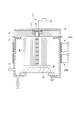
- the film forming apparatus 1 according to the present embodiment includes a chamber 2, a cathode unit C, a first magnetic field generation mechanism 7, a DC power supply 9, a gas introduction mechanism 11, and an exhaust.
- the mechanism 12 and the second magnetic field generation mechanism 13 are provided at least.
- the ceiling part side of the chamber 2 will be described as “upper”, and the bottom part side will be described as “lower”.
- the chamber 2 is an airtight container that can form a vacuum atmosphere.
- the chamber 2 has an internal space in which the substrate W and the target 5 are opposed to each other and the substrate W and the target 5 are accommodated. Further, a stage 10 is disposed at the bottom of the chamber 2 so as to face the target 5, and the substrate W can be positioned and held.
- the chamber 2 is electrically connected to the ground potential.
- being connected to the ground potential means a ground potential state or a grounded state.
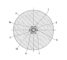
- the cathode unit C includes a disc-shaped holder 3 made of a conductive material.
- the holder 3 can be made of the same material as the target 5 described later, for example.
- the target 5 is a hollow type (bottom cylindrical shape; inverted U-shaped cross section) target 5. A case where the cathode unit C including the hollow type (reverse U-shaped) target 5 according to the present embodiment is attached to the ceiling portion of the chamber 2 will be described.
- the target 5 is made of a material appropriately selected according to the composition of the thin film formed on the substrate W to be processed, for example, Cu, Ti, or Ta.
- the target 5 has, for example, a bottomed cylindrical outer shape in which a discharge space 5a is formed.
- the target 5 is mounted in a recess 4 formed in the holder 3 and is disposed at an upper position (inside the ceiling side) in the internal space of the chamber 2.
- This target 5 is connected to a DC power source 9 provided outside the chamber 2.
- the recess 4 is formed on the lower surface of the holder 3 and is concentric with the center Cp (see FIG. 3) of the holder 3 and has a circular shape in plan view.
- the target 5 is detachably fitted into the recess 4 from the bottom side. That is, the opening of the target 5 faces the substrate side.
- the lower surface of the target 5 coincides with the lower surface of the holder 3 in a horizontal plane (becomes flush). That is, the length of the target 5 matches the length of the recess 4.
- a mask plate (not shown) having an opening smaller than the opening area of the target 5 is attached to the lower surface of the holder 3.
- the mask 5 prevents the target 5 from being detached from the recess 4.
- the mask plate can be made of the same material as the target 5, for example.
- the first magnetic field generation mechanism 7 is, for example, a magnet formed in a rod shape, a cylindrical shape, or a prism shape, and generates a magnetic field in a space in front of the sputtering surface of the target 5.
- the first magnetic field generation mechanism 7 is assembled to the holder 3 to generate a magnetic field in the space inside the target 5.
- the first magnetic field generation mechanism (magnet) 7 is inserted into the accommodation hole 6 formed on the upper surface of the holder 3.
- the accommodation hole 6 is opened on the upper surface of the holder 3 and extends in the thickness direction. Therefore, the accommodation hole 6 is disposed along the depth direction of the recess 4, and the first magnetic field generation mechanism 7 can be accommodated on the surface (opposite surface) opposite to the one surface where the recess 4 is formed.
- the first magnetic field generation mechanism 7 can be easily assembled to the holder 3 by opening the accommodation hole 6. That is, the first magnetic field generating mechanism 7 can be easily assembled to the holder 3 by forming the concave portion on one surface of the holder 3 and forming the accommodation hole 6 on the other surface. In the following description, the first magnetic field generation mechanism 7 may be described as a magnet 7.
- the depth from the upper surface of the holder 3 is set so that the magnet 7 is located from the bottom of the target 5 to a depth position of at least about 1/3. That is, the accommodation hole 6 is formed up to a position about 1/3 of the depth of the target 5.
- the magnet 7 is designed so that a strong magnetic field of 500 gauss or more is generated in the space 5 a inside the target 5 when arranged around the recess 4.
- the magnet 7 is provided upright at a predetermined position of the disc-shaped support plate 8 (for example, the polarity on the support plate 8 side is N pole).
- each magnet 7 is inserted into each accommodation hole 6, and each magnet 7 is arranged around the recess 4 (see FIG. 2).
- the support plate 8 is also formed of a conductive material, and after both are joined, for example, both are fixed using a fastening mechanism such as a bolt. Note that a mechanism for circulating the refrigerant in the internal space of the support plate 8 may be provided to serve as a backing plate for cooling the holder 3 in which the target 5 is inserted during sputtering.
- the magnet (first magnetic field generating mechanism) 7 is integrally attached to the support plate 8, the magnet 7 is inserted into the accommodation hole 6 by joining the support plate 8 to the upper surface of the holder 3.
- the magnet 7 that is inserted and is disposed around the recess 4 as the first magnetic field generation mechanism may be more easily arranged.
- the DC power source 9 is a so-called sputtering power source that applies a negative DC voltage to the target during sputtering (or applies a DC voltage to make the sputtering surface of the target negative potential), and has a known structure. Have.
- the DC power source 9 is electrically connected to the cathode unit C (target 5).
- the gas introduction mechanism 11 adjusts the flow rate of the sputtering gas introduced into the chamber 2 and introduces a sputtering gas such as argon gas through a gas pipe connected to the side wall of the chamber 2. Further, the other end of the gas pipe communicates with a gas source via a mass flow controller (not shown).
- the exhaust mechanism 12 decompresses the inside of the chamber 2, and is composed of, for example, a turbo molecular pump or a rotary pump, and is connected to an exhaust port formed on the bottom wall of the vacuum chamber 2. As shown in FIG. 1, when the exhaust mechanism 12 is activated, the inside of the chamber 2 is evacuated from the exhaust port via the exhaust pipe 12a.
- the second magnetic field generation mechanism 13 generates a magnetic field so that perpendicular magnetic lines M pass locally at a predetermined interval from the sputtering surface of the target 5 toward the film formation surface of the substrate W.
- the second magnetic field generation mechanism 13 includes, for example, a coil formed by winding a conducting wire 15 around a ring-shaped yoke 14 provided on the outer wall of the chamber 2 around a reference axis CL connecting the target 5 and the substrate W. And a power supply device 16 for energizing the coil.
- the coil includes an upper coil 13u disposed above and a lower coil 13d disposed below.
- the second magnetic field generation mechanism 13 can control the flight direction of the sputtered particles by adjusting the strength of the magnetic field.
- the number of coils 13, the diameter and the number of turns of the conductive wire 15 are, for example, the size of the target 5, the distance between the target 5 and the substrate W, the rated current value of the power supply device 16 and the strength of the magnetic field to be generated ( (Gauss) is set as appropriate (for example, a diameter of 14 mm and a winding number of 10).
- the film thickness distribution in the plane of the substrate W during film formation is made substantially uniform (sputter rate). Is substantially uniform in the radial direction of the substrate W), the distance between the lower end of the upper coil 13u and the target 5 and the distance between the upper end of the lower coil 13d and the substrate W are the midpoints of the reference axis. It is preferable to set the vertical position of each coil 13u, 13d so as to be shorter than the distance to Cp. In this case, the distance between the lower end of the upper coil 13u and the target 5 and the distance between the upper end of the lower coil 13d and the substrate W do not necessarily need to be the same.
- the coils 13u and 13d may be provided on the back side of the target 5 and the substrate W.
- the power supply device 16 has a known structure including a control circuit (not shown) that can arbitrarily change the current value and the direction of the current to the upper and lower coils 13u and 13d.
- FIG. 1 shows a configuration in which separate power supply devices 16 are provided. When the coils 13u and 13d are energized in the direction, a configuration in which energization is performed by one power supply device may be employed.
- the film forming apparatus 1 By configuring the film forming apparatus 1 as described above, when the target 5 is sputtered, if the sputtered particles scattered from the target 5 have a positive charge, a vertical magnetic field from the target 5 to the substrate W The flight direction is controlled, and the sputtered particles are incident on and adhere to the substrate W substantially perpendicularly on the entire surface of the substrate W. As a result, if the film forming apparatus 1 of this embodiment is used in a film forming process in the manufacture of a semiconductor device, it is possible to realize an improvement in the coverage ratio to a fine groove or hole having a high aspect ratio.
- a silicon oxide film (insulating film) is formed on the surface of the Si wafer as the substrate W to be formed, and then a known method is used in the silicon oxide film.
- An example of forming a Cu film as a seed film by sputtering using a pattern formed by patterning fine holes for wiring will be described.
- the target 5 is fitted into the recess 4 on the lower surface of the holder 3, and the support plate 8 on which the magnet 7 is erected is placed on the upper surface of the holder 3 so that each magnet 7 is inserted into each receiving hole 6 of the holder 3.
- the indicator plate 8 and the holder 3 are fixed using, for example, bolts, and the cathode unit C is assembled. Then, the cathode unit C is attached to the ceiling portion of the chamber 2.
- the exhaust mechanism (exhaust pump) 12 is operated to evacuate the chamber 2 to a predetermined degree of vacuum (for example, 10 ⁇ 5 Pa).
- the power supply device 16 is input to energize the coils 13u and 13d, and magnetic lines M (FIG. 5) perpendicular to the target 5 from the sputtering surface toward the film formation surface of the substrate W are locally present at a predetermined interval. Generate a magnetic field to pass. At this time, the distance between the vertical magnetic force lines is the same in the central area and the peripheral area of the substrate W as the object to be processed.
- a sputtering gas made of, for example, Ar (argon) gas is supplied into the chamber 2 at a predetermined flow rate (that is, the gas pressure in the chamber 2 is 0.3 Pa or more and 10.
- the DC power supply 9 is activated and a negative potential having a predetermined value is applied (powered on) to the cathode unit C.
- argon ions or the like in the plasma collide with the inner wall surface of the target 5 and are sputtered, Cu atoms are scattered, and Cu atoms or ionized Cu ions are lower surfaces of the target 5 as indicated by dotted arrows in FIG.
- the substrate 2 is discharged into the chamber 2 toward the substrate W with strong straightness.
- the high-pressure process gas shortens the mean free path (MFP) in the chamber space and weakens the straightness, and as shown by arrows in FIG.
- the flight direction is controlled along the direction of the magnetic force lines M according to the shape of the vertical magnetic force lines M locally generated at a predetermined interval from the sputtering surface of the target 5 toward the substrate W, and is indicated by a dotted arrow in the figure.
- the directivity is enhanced so that a film is selectively formed only in a predetermined region (or a film is not selectively formed in the predetermined region).
- the film is formed with extremely high film thickness uniformity. Films can be formed with good coverage even for fine holes with a high aspect ratio. At this time, the growth of the thin film can be promoted by supplying energy by heat, ion irradiation or the like.
- the substrate W is disposed in the chamber 2 so as to face the target 5 that forms the base material of the coating, and the sputtering surface of the target 5 is placed on the deposition surface of the substrate W that is the object to be processed.
- a sputtering gas is introduced into the chamber 2 while generating a magnetic field so that perpendicular magnetic field lines pass locally at predetermined intervals, and the gas pressure in the chamber is in a range of 0.3 Pa to 10.0 Pa.
- the sputtered particles with uniform directivity can be transported from the sputtering source toward the substrate, and the direction of the sputtered particles from the target 5 is changed by a perpendicular magnetic field, so that it is substantially the same as the substrate W.
- a film forming apparatus according to this embodiment is used in a film forming process in manufacturing a semiconductor device, it is possible to form a film with high coverage even for a fine hole with a high aspect ratio.
- the transport path of sputtered particles can be controlled, if the sputtered particles are controlled so as to be limited only to the substrate, the amount of deposition on a portion other than the substrate such as an adhesion preventing plate can be greatly reduced. An extension of the maintenance cycle can be achieved.
- a plurality of cathode units as in the prior art are not provided in the film forming apparatus itself, the structure is simple and the manufacturing cost of the apparatus can be reduced as compared with the case where the apparatus configuration is changed.
- a rod-shaped magnet 7 is used as an example.
- the form is particularly limited. There is no. Therefore, a ring-shaped magnet may be used, and the space 5 a of the target 5 may be disposed so as to surround the target 5. In this case, it is only necessary to provide an annular housing groove on the upper surface of the holder 3 that can accommodate a ring-shaped magnet.
- the form in which the target 5 is detachably inserted into the holder 3 in consideration of mass productivity and target usage efficiency has been described.
- the holder 3 itself may serve as the target 5.
- a configuration in which only the recess 4 is formed on the lower surface of the holder 3, the magnet 7 is built around the recess 4, and the inner wall surface of the recess 4 is sputtered may be employed.
- a high-frequency power source (not shown) having a known structure is electrically connected to the stage, and a predetermined bias potential is applied to the stage 10 and eventually the substrate W during sputtering to form a Cu seed layer.
- a configuration in which Cu ions are actively drawn into the substrate to increase the sputtering rate may be employed.
- the case where the distance between the vertical magnetic lines M is the same in the central area and the peripheral area of the substrate W has been described.
- the current values applied to the upper and lower coils 13u and 13d by the power supply device 16 are respectively described.
- a configuration in which the intervals between the vertical magnetic force lines M are different in the central region and the peripheral region of the substrate W may be adopted. In this way, the strength of the magnetic field is adjusted, and the flight direction of the sputtered particles can be controlled to form a film in a desired region.
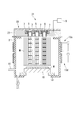
- a film forming apparatus 21 is an apparatus for forming a film on a surface of a substrate W as an object to be processed using a sputtering method. It is.
- This film forming apparatus 21 includes at least the chamber 2, the cathode unit C 1, the first magnetic field generation mechanism 7, the DC power supply 9, the gas introduction mechanism 11, the exhaust mechanism 12, and the second magnetic field generation mechanism 13.
- the same components as those in the first embodiment are denoted by the same reference numerals, the description thereof is omitted, and the same unless otherwise described.
- the cathode unit C1 includes a disc-shaped holder 23 made of a conductive material in plan view.
- the holder 23 can be made of, for example, the same material as a target described later.
- one concave portion 4 is formed concentrically with the center Cp of the holder 23, and six concave portions 4 are formed around the concave portion 4 with the same virtual circle as a reference. It is formed so as to be located on the circumference Vc at equal intervals. That is, in the present embodiment, one recess 4 formed at the center Cp of the holder 23 and six recesses 4 formed at equal intervals around the center Cp of the holder 23 are illustrated. Has been.
- each recess 4 is formed around the recesses 4 formed at the center Cp of the holder.
- the periphery of each recess 4 on the virtual circumference Vc is the reference. It is also possible to form six recesses 4 each.
- a plurality of recesses 4 may be formed on the outer side in the radial direction of the holder 23 (until the recesses 4 cannot be formed), and the recesses 4 may be densely formed over the entire lower surface of the holder 23. .
- the area of the lower surface of the holder is sized so that the center of the concave portion 4 positioned at the outermost radial direction of the holder is positioned radially inward from the outer periphery of the substrate W.
- one cycle of recesses (six) are formed around the recess 4 formed at the center Cp of the holder.
- recesses of 2 cycles or more may be formed.
- the number of recesses is not limited to six, and for example, four or eight recesses may be used.
- the interval in the radial direction between the recesses 4 is set in a range that is larger than the diameter of a cylindrical magnet, which will be described later, and the strength of the holder 23 can be maintained.
- a target 5 is inserted into each recess 4, and the target 5 is detachably fitted to each recess 4 from the bottom side.
- the receiving hole 6 is formed so that the six magnets 7 are arranged at equal intervals around the one recess 4 and on a line connecting the centers of the respective recesses 4 adjacent to each other. (See FIG. 9).
- Each magnet 7 is designed so that a strong magnetic field of 500 gauss or more is generated in the space 5 a inside the target 5 when arranged around each recess 4.
- the film forming apparatus 21 By forming the film forming apparatus 21 as described above, when the target 5 is sputtered and the sputtered particles scattered from the target 5 have a positive charge, a vertical magnetic field from the target 5 to the substrate W
- the flight direction is controlled, and sputtered particles are incident on and adhere to the substrate W substantially perpendicularly on the entire surface of the substrate W. That is, as indicated by arrows in FIG. 7, along the direction of the magnetic force lines M in accordance with the shape of the vertical magnetic force lines M generated locally at a predetermined interval from the sputtering surface of the target 5 toward the substrate W.
- the flight direction is controlled, and the directivity is enhanced so as to selectively form a film only in a predetermined region (or not to selectively form a film in the predetermined region) as indicated by a dotted arrow in the figure.
- the film forming apparatus 21 according to the present embodiment when used in the film forming process in the manufacture of the semiconductor device, it is possible to improve the coverage ratio to the fine grooves or holes having a high aspect ratio.
- a film having extremely high film thickness uniformity is formed at a position facing a plurality of openings of the target 5, thereby forming high-aspect-ratio fine holes in a plurality of predetermined regions on the substrate W.
- a film can be formed with good coverage.
- Example 1 sputtering is performed by adjusting the process pressure while generating a magnetic field so that perpendicular magnetic field lines pass locally at a predetermined interval from the sputtering surface of the target toward the deposition surface of the substrate.
- the process pressure in the chamber is set to 0.12 Pa, 0.3 Pa, 0.6 Pa, 1.2 Pa, 1.6 Pa, using the film forming apparatus shown in FIG. A Cu film was formed on the substrate W by changing the pressure to 3.0 Pa and 10.0 Pa.
- a silicon oxide film is formed over the entire surface of a ⁇ 300 mm Si wafer as the substrate W, and then a high aspect ratio fine hole (for example, having a width w of, for example) is formed in the silicon oxide film by a known method. 45 nm and depth d was 150 nm) were used for patterning. Further, as the cathode unit, as shown in FIG. 2, a Cu holder having a composition ratio of 99% and having a diameter of 600 mm was used.
- a concave portion having an opening diameter of 40 mm and a depth of 50 mm was formed at the center of the lower surface of the holder, and a bottomed cylindrical target made of the same material as the holder was fitted into the concave portion from the bottom side. Further, around the recess, six magnet units were incorporated at equal intervals in the circumferential direction to obtain a cathode unit for Example 1. In this case, the magnet generates a magnetic field with a magnetic field intensity of 500 gauss in the space of the recess. And after attaching the cathode unit produced in this way to the ceiling part of a vacuum chamber, the mask member was mounted
- the distance between the bottom surface of the holder and the substrate is set to 300 mm
- Ar is used as the sputtering gas
- the power input to the target is set to 20
- a constant current control is set to 20 seconds.
- the Cu film was formed by setting. And the film thickness in the center position (0 mm) of the board
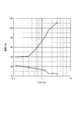
- FIG. 10 shows the relationship between the process pressure and the film thickness.
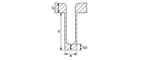
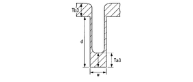
- the film-forming state in the said fine hole when the gas pressure in a chamber is (A) 0.12 Pa, (B) 0.6 Pa, (C) 1.6 Pa is a typical cross section.
- the film thickness Ta on the surface around the fine hole and the film thickness Tb on the bottom surface of the fine hole were measured, and the bottom coverage (Tb / Ta) was calculated. .
- the film thickness Ta1 on the surface around the fine hole is 40 nm
- the film thickness Tb1 on the bottom surface of the fine hole is 24.3 nm
- the bottom coverage is 60. It was 8%.
- the film thickness Ta2 on the surface around the fine hole is 40 nm
- the film thickness Tb2 on the bottom surface of the fine hole is 35.0 nm
- the bottom coverage is 87.9. %Met.
- the film thickness Ta3 on the surface around the fine hole is 40 nm
- the film thickness Tb3 on the bottom surface of the fine hole is 42.4 nm
- the bottom coverage is 106. %Met.
- zone (A) when the pressure at the time of film formation is 0.3 Pa or less, zone (A), and when the pressure at the time of film formation is 0.3 Pa or more and 1.5 Pa or less, zone (B) When the pressure at the time of film formation is 1.5 Pa or more and 10.0 or less as zone (C), and when the pressure at the time of film formation is 10.0 Pa or more as zone (D), the film is formed in each zone.
- the bottom coverage of the coating, the directivity of the sputtered particles, and the convergence of the sputtered particles were evaluated. The results are shown in Table 2. In addition, the result in each evaluation method shows the following, respectively.
- the bottom coverage was 50% or less, it was NG, when it was 50% to 80%, B, when it was 80% to 100%, F, and when 100% or more, it was G.
- the mark is NG, the mark B is large, the mark F is medium, and the mark G is almost impossible.
- the convergence of the sputtered particles is such that the film thickness ratio at the position corresponding to the lower part of the erode and the lower part of the non-erode is NG mark when the ratio is 1 or less, B mark when it is about 1-2, 2-5
- the F mark was given when the degree was 5 and the G mark was given when it was 5 or more.
- the sputtering gas is introduced into the chamber while generating a magnetic field so that perpendicular magnetic lines of force pass locally from the sputtering surface of the target toward the deposition surface of the substrate, and the gas in the chamber is introduced.
- Sputtered particles are formed on the deposition surface of the substrate while controlling the flight direction of the generated sputtered particles by sputtering the target while controlling the pressure within a range of 0.3 Pa or higher, preferably 1.5 Pa or higher and 10.0 Pa or lower. It can be seen that the film can be formed by inducing and depositing.
- Example 1 In order to confirm that the flight direction of the sputtered particles can be controlled by adjusting the strength of the magnetic field, the desired result is obtained in Example 1 under the same process conditions as in Example 1.
- 1.6 Pa gas flow rate is 267 sccm
- the film thickness at the directional position was measured.
- FIG. 12 shows film thickness distributions showing the relationship between the substrate position and the film thickness at this time.
- a sputtering gas is introduced into the chamber while generating a magnetic field so that perpendicular magnetic lines of force pass locally at a predetermined interval from the sputtering surface of the target toward the film formation surface of the target object. If the internal gas pressure is controlled within the range of 0.3 Pa or more and 10.0 Pa or less, it can be carried out even when a planar type target is used.
- the film forming method according to the present invention is outlined below.
- the object to be processed W and a target 5 are disposed to face each other in a chamber 2 having an internal space that can be decompressed, and the object to be processed is formed from the sputtering surface of the target.
- a magnetic field is generated toward the film surface so that perpendicular magnetic field lines pass locally at predetermined intervals.
- a sputtering gas is introduced into the chamber so that the gas pressure in the chamber is controlled to be in a range of 0.3 Pa to 10.0 Pa, and a negative DC voltage is applied to the target. Plasma is generated in the space between.
- the flying direction of the sputtered particles generated by sputtering the target the sputtered particles are guided to the object to be processed and deposited to form a film on the surface of the object to be processed.
- the flying direction of the sputtered particles can be controlled by adjusting the strength of the magnetic field.
- the distance between the vertical magnetic lines of force may be the same or different in the central area and the peripheral area of the object to be processed.
- the film forming apparatus and film forming method of the present invention can be widely used for forming a film in a fine groove or hole having a high aspect ratio. Furthermore, the film forming apparatus and the film forming method of the present invention can improve the coverage rate and extend the maintenance cycle of the film forming apparatus.
Landscapes
- Chemical & Material Sciences (AREA)
- Engineering & Computer Science (AREA)
- Physics & Mathematics (AREA)
- Plasma & Fusion (AREA)
- Analytical Chemistry (AREA)
- Chemical Kinetics & Catalysis (AREA)
- Materials Engineering (AREA)
- Mechanical Engineering (AREA)
- Metallurgy (AREA)
- Organic Chemistry (AREA)
- Physical Vapour Deposition (AREA)
- Electrodes Of Semiconductors (AREA)
Abstract
Description
本願は、2009年05月20日に、日本に出願された特願2009-121894号に基づき優先権を主張し、その内容をここに援用する。
例えば、特許文献2には、基板を固定する静電チャックプレートの表面にダミー基板を載置し、静電吸着により密着させた後、真空槽内にフッ素ガス等のクリーニングガスを導入することにより、真空チャンバの内部壁面等に付着したターゲットの構成物質等の薄膜をエッチングする技術が開示されている。
また、特許文献3には、半導体ウエハに硫酸過水洗浄とアンモニア過水洗浄を実施することで、静電チャックプレートからのパーティクルを除去する技術が開示されている。
さらに、例えば特許文献4には、成膜材料供給源(ターゲット)からの材料を遮断するシャッター機構を備え、このシャッター機構を構成するシャッター板を定期的に清浄するか取り替える成膜装置が開示されている。
しかも、上記特許文献2及び特許文献4に記載された技術は、その装置構成が複雑となり、やはりコスト高を招くという不具合がある。
本発明に係る成膜方法は、被処理体の表面に被膜を形成する成膜方法であって、チャンバ内に、前記被膜の母材をなすターゲットと、前記被処理体とを対向配置し、前記ターゲットのスパッタ面から前記被処理体の被成膜面に向けて、所定の間隔で垂直な磁力線が局所的に通る磁場を発生させつつ、前記チャンバ内にスパッタガスを導入して、前記チャンバ内におけるガス圧が0.3Pa以上10.0Pa以下の範囲に制御するとともに、前記ターゲットに負の直流電圧を印加することにより、前記ターゲットと前記被処理体との間の空間にプラズマを発生させて、前記ターゲットをスパッタリングすることにより生じたスパッタ粒子の飛翔方向を制御しながら、前記スパッタ粒子を前記被処理体へ誘導して堆積させて、前記被膜を形成する。
したがって、高アスペクト比の微細溝又は穴へのカバレージ率の向上を実現することができ、しかも、成膜装置のメンテナンス周期の延長が達成できる。
したがって、簡単な構成かつ低コストで、高アスペクト比の微細溝又は穴へのカバレージ率の向上を実現することができると共に、メンテナンス周期が延長された成膜装置とすることができる。
本発明に係る成膜方法を実施する成膜装置1は、被処理体としての基板Wの表面にスパッタ法を用いて被膜を形成する装置である。本実施形態にかかる成膜装置1は、図1~図3に示すように、チャンバ2と、カソードユニットCと、第一磁場発生機構7と、直流電源9と、ガス導入機構11と、排気機構12と、第二磁場発生機構13と、を少なくとも備える。
なお、以下の説明において、チャンバ2の天井部側を「上方」とし、その底部側を「下方」として説明する。
チャンバ2は、真空雰囲気を形成することが可能である気密容器である。このチャンバ2は、基板Wとターゲット5とを対向配置させて、基板Wとターゲット5とを収納する内部空間を有する。
また、チャンバ2の底部には、ターゲット5に対向させてステージ10が配置され、基板Wを位置決め保持できる。
なお、チャンバ2は、電気的に接地電位に接続されている。ここで、接地電位に接続されているとは、グラウンド電位状態又はアースした状態を示す。
本実施形態に係るホロータイプ(逆U字状)のターゲット5を備えたカソードユニットCを、チャンバ2の天井部に取り付けた場合について説明する。
この磁石7は、凹部4の周囲に配置したときにターゲット5の内部の空間5aに500ガウス以上の強磁場が発生するように設計されている。なお、この磁石7は、円板状の支持板8の所定位置にその極性を一致させて(例えば、支持板8側の極性をN極として)立設されている。
この第二磁場発生機構13は、例えば、ターゲット5と基板Wとを結ぶ基準軸CLの回りでチャンバ2の外側壁に設けたリング状のヨーク14に導線15を巻回してなるコイルと、このコイルを通電させる電源装置16とを備える。
本実施形態において、コイルは、上方に配された上コイル13uと、下方に配された下コイル13dとを備えている。
なお、この際、熱やイオン照射等によりエネルギーを供給することで、薄膜の成長を促すことができる。
このようにすると、磁場の強度が調整され、スパッタ粒子の飛翔方向を制御して、所望の領域に成膜することができる。
上記第1の実施形態では、ホルダの片面にターゲット(材)が1つだけ取り付けられたカソードユニットを備える形態について説明したが、本発明はこれのみに限定されない。
したがって、本実施形態では、ホルダの片面に複数のターゲット(材)が取り付けられたカソードユニットを備える成膜装置について説明する。
なお、以下に説明する第2の実施形態において、上述した第1の実施形態と異なる部分を中心に説明する。したがって、第1の実施形態と同様の構成部分は同じ符号を付し、その説明は省略し、特に説明しない限り同じである。
また、カソードユニットとして、図2に示すように、組成比が99%で、φ600mmに作製したCu製のホルダを用いた。そして、このホルダの下面中央に開口径φ40mm、深さ50mmの凹部を形成し、この凹部内に、ホルダと同一材料から作製された有底筒状のターゲットをその底部側から嵌着した。また、凹部の周囲には、周方向に等間隔で6個の磁石ユニットを内蔵し、実施例1用のカソードユニットとした。この場合、磁石は、凹部の空間に500ガウスの磁場強度で磁場を発生させる。そして、このように作製したカソードユニットを真空チャンバの天井部に取付けた後、凹部の開口を除くホルダ下面にマスク部材を装着して覆った。
そして、成膜した基板Wの中心位置(0mm)と、この中心位置を基準として70mm離れた位置での膜厚をそれぞれ測定した。その結果を表1に示す。また、プロセス圧力と膜厚との関係を図10に示す。

これにより、チャンバ内におけるプロセス圧力を0.3Pa以上、好ましくは1.5Pa以上に制御すると、指向性を高められることが分かる。
なお、各評価方法における結果は、それぞれ以下のことを示す。
ボトムカバレッジが、50%以下のときはNG印、50%~80%のときはB印、80%~100%のときはF印、100%以上のときはG印とした。
また、スパッタ粒子の指向性によりカバレージのシンメトリーが著しく大きくなるときはNG印、大きいときはB印、中程度のときはF印、ほとんど確認できないときはG印とした。
さらに、スパッタ粒子の収束性は、エロード部の下方と非エロード部の下方に相当する位置における膜厚比が、1以下のときはNG印、1~2程度のときはB印、2~5程度のときはF印、5以上のときはG印とした。

したがって、ターゲットのスパッタ面から基板の被成膜面に向けて所定の間隔で垂直な磁力線が局所的に通るように磁場を発生させながら、チャンバ内にスパッタガスを導入して、チャンバ内におけるガス圧を0.3Pa以上、好ましくは1.5Pa以上10.0Pa以下の範囲に制御してターゲットをスパッタリングすることで、生じたスパッタ粒子の飛翔方向を制御しながら基板の被成膜面へスパッタ粒子を誘導し、堆積させて成膜できることが分かる。
したがって、磁場の強度を調整することで、スパッタ粒子の飛翔方向を制御できることが分かる。
被処理体の表面に被膜を形成する成膜方法において、減圧可能な内部空間を有するチャンバ2内に被処理体Wとターゲット5とを対向配置し、ターゲットのスパッタ面から被処理体の被成膜面に向けて、所定の間隔で垂直な磁力線が局所的に通るように磁場を発生させる。次いで、チャンバ内にスパッタガスを導入して、チャンバ内におけるガス圧が0.3Pa以上10.0Pa以下の範囲に制御するとともに、ターゲットに負の直流電圧を印加することにより、ターゲットと処理体との間の空間にプラズマを発生させる。そして、ターゲットをスパッタリングすることにより生じたスパッタ粒子の飛翔方向を制御しながらスパッタ粒子を被処理体へ誘導し、堆積させて、被処理体の表面に被膜を形成する。
前にも説明したように、前記磁場の強度を調整することにより、前記スパッタ粒子の飛翔方向を制御することができる。さらに、被処理体の中央域と周縁域において、垂直な磁力線どうしの間隔が同一でも異なっても良い。
1,21 成膜装置
2 チャンバ
3,23 ホルダ
4 凹部
5 ターゲット
5a 放電用の空間
6 収容孔
7 磁石(第一磁場発生機構)
8 支持板
9 直流電源(DC電源)
10 ステージ
11 ガス管(ガス導入機構)
12 排気ポンプ(排気機構)
13u 上コイル(第二磁場発生機構)
13d 下コイル(第二磁場発生機構)
14 ヨーク
15 導線
16 電源装置
Claims (6)
- 被処理体の表面に被膜を形成する成膜方法であって、
チャンバ内に、前記被膜の母材をなすターゲットと、前記被処理体とを対向配置し、前記ターゲットのスパッタ面から前記被処理体の被成膜面に向けて、所定の間隔で垂直な磁力線が局所的に通る磁場を発生させつつ、
前記チャンバ内にスパッタガスを導入して、前記チャンバ内におけるガス圧を0.3Pa以上10.0Pa以下の範囲に制御するとともに、前記ターゲットに負の直流電圧を印加することにより、前記ターゲットと前記被処理体との間の空間にプラズマを発生させ、
前記ターゲットをスパッタリングすることにより生じたスパッタ粒子の飛翔方向を制御しながら、前記スパッタ粒子を前記被処理体へ誘導して堆積させて、前記被膜を形成することを特徴とする成膜方法。 - 前記磁場の強度を調整することにより、前記スパッタ粒子の飛翔方向を制御することを特徴とする請求項1に記載の成膜方法。
- 前記被処理体の中央域と周縁域において、前記垂直な磁力線どうしの間隔が同一であることを特徴とする請求項1又は請求項2に記載の成膜方法。
- 前記被処理体の中央域と周縁域において、前記垂直な磁力線どうしの間隔が異なることを特徴とする請求項1又は請求項2に記載の成膜方法。
- 被処理体の表面に被膜を形成する成膜装置であって、
前記被膜の母材をなすターゲットと前記被処理体とを対向配置させて、前記ターゲット及び前記被処理体を収納する内部空間を有するチャンバと;
前記チャンバ内を減圧する排気機構と;
前記ターゲットのスパッタ面から見て前方の空間に磁場を発生させる第一磁場発生機構と;
前記チャンバ内に導入するスパッタガスの流量を調整する機能を備えたガス導入機構と;
前記ターゲットに負の直流電圧を印加する直流電源と;
前記ターゲットの前記スパッタ面から前記被処理体の被成膜面に向けて、所定の間隔で垂直な磁力線が局所的に通る磁場を発生させる第二磁場発生機構と;
を備えることを特徴とする成膜装置。 - 片面に1つ以上の凹部が設けられたホルダをさらに備え;
前記ターゲットは有底筒状を形成し、前記ホルダの前記凹部に、前記ターゲットの底部側から装着され;
前記第一磁場発生機構は、前記ターゲットの内部空間に磁場を発生させるように、前記ホルダに組み付けられている、ことを特徴とする請求項5に記載の成膜装置。
Priority Applications (6)
| Application Number | Priority Date | Filing Date | Title |
|---|---|---|---|
| US13/321,605 US20120118725A1 (en) | 2009-05-20 | 2010-05-20 | Film forming method and film forming apparatus |
| JP2011514342A JP5417437B2 (ja) | 2009-05-20 | 2010-05-20 | 成膜方法及び成膜装置 |
| DE112010002029T DE112010002029T8 (de) | 2009-05-20 | 2010-05-20 | Filmbildungsverfahren und Filmbildungsvorrichtung |
| KR1020117028442A KR101344085B1 (ko) | 2009-05-20 | 2010-05-20 | 성막 방법 및 성막 장치 |
| CN2010800216519A CN102428209A (zh) | 2009-05-20 | 2010-05-20 | 成膜方法以及成膜装置 |
| SG2011085743A SG176182A1 (en) | 2009-05-20 | 2010-05-20 | Film-forming method and film-forming apparatus |
Applications Claiming Priority (2)
| Application Number | Priority Date | Filing Date | Title |
|---|---|---|---|
| JP2009-121894 | 2009-05-20 | ||
| JP2009121894 | 2009-05-20 |
Publications (1)
| Publication Number | Publication Date |
|---|---|
| WO2010134346A1 true WO2010134346A1 (ja) | 2010-11-25 |
Family
ID=43126037
Family Applications (1)
| Application Number | Title | Priority Date | Filing Date |
|---|---|---|---|
| PCT/JP2010/003406 Ceased WO2010134346A1 (ja) | 2009-05-20 | 2010-05-20 | 成膜方法及び成膜装置 |
Country Status (8)
| Country | Link |
|---|---|
| US (1) | US20120118725A1 (ja) |
| JP (1) | JP5417437B2 (ja) |
| KR (1) | KR101344085B1 (ja) |
| CN (1) | CN102428209A (ja) |
| DE (1) | DE112010002029T8 (ja) |
| SG (1) | SG176182A1 (ja) |
| TW (1) | TWI464285B (ja) |
| WO (1) | WO2010134346A1 (ja) |
Cited By (2)
| Publication number | Priority date | Publication date | Assignee | Title |
|---|---|---|---|---|
| WO2012070195A1 (ja) * | 2010-11-24 | 2012-05-31 | 株式会社アルバック | スパッタリング方法 |
| JP2013001965A (ja) * | 2011-06-16 | 2013-01-07 | Ulvac Japan Ltd | スパッタリング方法 |
Families Citing this family (8)
| Publication number | Priority date | Publication date | Assignee | Title |
|---|---|---|---|---|
| TWI565527B (zh) * | 2011-12-26 | 2017-01-11 | 鴻海精密工業股份有限公司 | 電漿成膜裝置 |
| US9576810B2 (en) * | 2013-10-03 | 2017-02-21 | Applied Materials, Inc. | Process for etching metal using a combination of plasma and solid state sources |
| KR102502558B1 (ko) * | 2018-08-10 | 2023-02-23 | 가부시키가이샤 아루박 | 스패터링 장치 |
| KR102611646B1 (ko) * | 2018-08-27 | 2023-12-11 | 가부시키가이샤 알박 | 스퍼터링 장치 및 성막 방법 |
| JP7202815B2 (ja) * | 2018-08-31 | 2023-01-12 | キヤノントッキ株式会社 | 成膜装置、成膜方法、および電子デバイスの製造方法 |
| CN110777345A (zh) * | 2019-11-28 | 2020-02-11 | 湖南华庆科技有限公司 | 一种磁控光学镀膜设备 |
| WO2022158271A1 (ja) * | 2021-01-19 | 2022-07-28 | 芝浦機械株式会社 | 表面処理装置および表面処理方法 |
| JP7747417B2 (ja) * | 2021-12-24 | 2025-10-01 | 東京エレクトロン株式会社 | プラズマ処理装置、およびプラズマ処理装置の製造方法 |
Citations (3)
| Publication number | Priority date | Publication date | Assignee | Title |
|---|---|---|---|---|
| JPS61246368A (ja) * | 1985-04-24 | 1986-11-01 | Nec Corp | 金属膜の堆積方法 |
| JPH06172995A (ja) * | 1992-12-09 | 1994-06-21 | Tokyo Electron Ltd | マグネトロンスパッタリング装置及びスパッタリングガン |
| JP2002504187A (ja) * | 1997-04-21 | 2002-02-05 | トーキョー エレクトロン アリゾナ インコーポレイテッド | 材料をイオン化スパッタリングする方法と装置 |
Family Cites Families (9)
| Publication number | Priority date | Publication date | Assignee | Title |
|---|---|---|---|---|
| JP3233496B2 (ja) | 1993-04-14 | 2001-11-26 | 株式会社アルバック | 真空成膜装置 |
| JP5026631B2 (ja) * | 1999-06-24 | 2012-09-12 | 株式会社アルバック | スパッタリング装置 |
| US6352629B1 (en) * | 2000-07-10 | 2002-03-05 | Applied Materials, Inc. | Coaxial electromagnet in a magnetron sputtering reactor |
| JP4073657B2 (ja) | 2001-11-21 | 2008-04-09 | 株式会社アルバック | 処理方法 |
| US7527713B2 (en) * | 2004-05-26 | 2009-05-05 | Applied Materials, Inc. | Variable quadruple electromagnet array in plasma processing |
| JP4717896B2 (ja) * | 2006-01-25 | 2011-07-06 | 株式会社アルバック | スパッタリング装置及び成膜方法 |
| JP2008047661A (ja) | 2006-08-14 | 2008-02-28 | Seiko Epson Corp | 成膜装置及び半導体装置の製造方法 |
| JP2008251579A (ja) | 2007-03-29 | 2008-10-16 | Matsushita Electric Ind Co Ltd | 静電チャックおよび半導体装置の製造方法 |
| JP2009121894A (ja) | 2007-11-14 | 2009-06-04 | Fujitsu Ltd | 導電体パターンの欠陥検査方法及び欠陥検査装置 |
-
2010
- 2010-05-20 CN CN2010800216519A patent/CN102428209A/zh active Pending
- 2010-05-20 KR KR1020117028442A patent/KR101344085B1/ko active Active
- 2010-05-20 DE DE112010002029T patent/DE112010002029T8/de not_active Ceased
- 2010-05-20 WO PCT/JP2010/003406 patent/WO2010134346A1/ja not_active Ceased
- 2010-05-20 TW TW099116172A patent/TWI464285B/zh active
- 2010-05-20 JP JP2011514342A patent/JP5417437B2/ja active Active
- 2010-05-20 SG SG2011085743A patent/SG176182A1/en unknown
- 2010-05-20 US US13/321,605 patent/US20120118725A1/en not_active Abandoned
Patent Citations (3)
| Publication number | Priority date | Publication date | Assignee | Title |
|---|---|---|---|---|
| JPS61246368A (ja) * | 1985-04-24 | 1986-11-01 | Nec Corp | 金属膜の堆積方法 |
| JPH06172995A (ja) * | 1992-12-09 | 1994-06-21 | Tokyo Electron Ltd | マグネトロンスパッタリング装置及びスパッタリングガン |
| JP2002504187A (ja) * | 1997-04-21 | 2002-02-05 | トーキョー エレクトロン アリゾナ インコーポレイテッド | 材料をイオン化スパッタリングする方法と装置 |
Cited By (3)
| Publication number | Priority date | Publication date | Assignee | Title |
|---|---|---|---|---|
| WO2012070195A1 (ja) * | 2010-11-24 | 2012-05-31 | 株式会社アルバック | スパッタリング方法 |
| JP5795002B2 (ja) * | 2010-11-24 | 2015-10-14 | 株式会社アルバック | スパッタリング方法 |
| JP2013001965A (ja) * | 2011-06-16 | 2013-01-07 | Ulvac Japan Ltd | スパッタリング方法 |
Also Published As
| Publication number | Publication date |
|---|---|
| US20120118725A1 (en) | 2012-05-17 |
| TWI464285B (zh) | 2014-12-11 |
| JPWO2010134346A1 (ja) | 2012-11-08 |
| JP5417437B2 (ja) | 2014-02-12 |
| KR20120023035A (ko) | 2012-03-12 |
| DE112010002029T5 (de) | 2012-08-02 |
| KR101344085B1 (ko) | 2013-12-24 |
| TW201107511A (en) | 2011-03-01 |
| SG176182A1 (en) | 2011-12-29 |
| DE112010002029T8 (de) | 2012-10-11 |
| CN102428209A (zh) | 2012-04-25 |
Similar Documents
| Publication | Publication Date | Title |
|---|---|---|
| JP5417437B2 (ja) | 成膜方法及び成膜装置 | |
| JP4970937B2 (ja) | 誘導性結合プラズマの均一性を改善する側壁磁石及びそれと共に使用するシールド | |
| US6462482B1 (en) | Plasma processing system for sputter deposition applications | |
| JP5550565B2 (ja) | スパッタリング装置及びスパッタリング方法 | |
| JPH01272765A (ja) | スパッタ被覆装置およびその被覆方法 | |
| US8911602B2 (en) | Dual hexagonal shaped plasma source | |
| WO2011002058A1 (ja) | 薄膜の成膜方法 | |
| WO2009157439A1 (ja) | スパッタリング装置及びスパッタリング方法 | |
| JP5717444B2 (ja) | カソードユニット及びこのカソードユニットを備えたスパッタリング装置 | |
| JP2013139642A (ja) | スパッタ成膜応用のためのプラズマ処理装置 | |
| JPH04228567A (ja) | プレーナー・マグネトロン・スパッタリングシステム | |
| JP3749178B2 (ja) | 切頭円錐形スパッタリングターゲットのためのターゲット利用率の高い磁気構成 | |
| CN116783324B (zh) | 磁控溅射装置用阴极单元及磁控溅射装置 | |
| JP2011017088A (ja) | スパッタ成膜応用のためのプラズマ処理装置 | |
| JPWO2012070195A1 (ja) | スパッタリング方法 | |
| JP2000256844A (ja) | スパッタ装置及び成膜方法 |
Legal Events
| Date | Code | Title | Description |
|---|---|---|---|
| WWE | Wipo information: entry into national phase |
Ref document number: 201080021651.9 Country of ref document: CN |
|
| 121 | Ep: the epo has been informed by wipo that ep was designated in this application |
Ref document number: 10777582 Country of ref document: EP Kind code of ref document: A1 |
|
| ENP | Entry into the national phase |
Ref document number: 2011514342 Country of ref document: JP Kind code of ref document: A |
|
| WWE | Wipo information: entry into national phase |
Ref document number: 112010002029 Country of ref document: DE Ref document number: 1120100020299 Country of ref document: DE |
|
| ENP | Entry into the national phase |
Ref document number: 20117028442 Country of ref document: KR Kind code of ref document: A |
|
| WWE | Wipo information: entry into national phase |
Ref document number: 13321605 Country of ref document: US |
|
| 122 | Ep: pct application non-entry in european phase |
Ref document number: 10777582 Country of ref document: EP Kind code of ref document: A1 |