WO2010131639A1 - 半導体装置およびその製造方法並びに太陽電池 - Google Patents
半導体装置およびその製造方法並びに太陽電池 Download PDFInfo
- Publication number
- WO2010131639A1 WO2010131639A1 PCT/JP2010/057936 JP2010057936W WO2010131639A1 WO 2010131639 A1 WO2010131639 A1 WO 2010131639A1 JP 2010057936 W JP2010057936 W JP 2010057936W WO 2010131639 A1 WO2010131639 A1 WO 2010131639A1
- Authority
- WO
- WIPO (PCT)
- Prior art keywords
- layer
- basi
- silicide
- tunnel
- silicon
- Prior art date
- Legal status (The legal status is an assumption and is not a legal conclusion. Google has not performed a legal analysis and makes no representation as to the accuracy of the status listed.)
- Ceased
Links
Images









Classifications
-
- H—ELECTRICITY
- H10—SEMICONDUCTOR DEVICES; ELECTRIC SOLID-STATE DEVICES NOT OTHERWISE PROVIDED FOR
- H10F—INORGANIC SEMICONDUCTOR DEVICES SENSITIVE TO INFRARED RADIATION, LIGHT, ELECTROMAGNETIC RADIATION OF SHORTER WAVELENGTH OR CORPUSCULAR RADIATION
- H10F77/00—Constructional details of devices covered by this subclass
- H10F77/10—Semiconductor bodies
- H10F77/12—Active materials
-
- H—ELECTRICITY
- H10—SEMICONDUCTOR DEVICES; ELECTRIC SOLID-STATE DEVICES NOT OTHERWISE PROVIDED FOR
- H10F—INORGANIC SEMICONDUCTOR DEVICES SENSITIVE TO INFRARED RADIATION, LIGHT, ELECTROMAGNETIC RADIATION OF SHORTER WAVELENGTH OR CORPUSCULAR RADIATION
- H10F10/00—Individual photovoltaic cells, e.g. solar cells
- H10F10/10—Individual photovoltaic cells, e.g. solar cells having potential barriers
- H10F10/16—Photovoltaic cells having only PN heterojunction potential barriers
-
- H—ELECTRICITY
- H10—SEMICONDUCTOR DEVICES; ELECTRIC SOLID-STATE DEVICES NOT OTHERWISE PROVIDED FOR
- H10F—INORGANIC SEMICONDUCTOR DEVICES SENSITIVE TO INFRARED RADIATION, LIGHT, ELECTROMAGNETIC RADIATION OF SHORTER WAVELENGTH OR CORPUSCULAR RADIATION
- H10F71/00—Manufacture or treatment of devices covered by this subclass
-
- H—ELECTRICITY
- H10—SEMICONDUCTOR DEVICES; ELECTRIC SOLID-STATE DEVICES NOT OTHERWISE PROVIDED FOR
- H10P—GENERIC PROCESSES OR APPARATUS FOR THE MANUFACTURE OR TREATMENT OF DEVICES COVERED BY CLASS H10
- H10P14/00—Formation of materials, e.g. in the shape of layers or pillars
- H10P14/20—Formation of materials, e.g. in the shape of layers or pillars of semiconductor materials
- H10P14/22—Formation of materials, e.g. in the shape of layers or pillars of semiconductor materials using physical deposition, e.g. vacuum deposition or sputtering
-
- H—ELECTRICITY
- H10—SEMICONDUCTOR DEVICES; ELECTRIC SOLID-STATE DEVICES NOT OTHERWISE PROVIDED FOR
- H10P—GENERIC PROCESSES OR APPARATUS FOR THE MANUFACTURE OR TREATMENT OF DEVICES COVERED BY CLASS H10
- H10P14/00—Formation of materials, e.g. in the shape of layers or pillars
- H10P14/20—Formation of materials, e.g. in the shape of layers or pillars of semiconductor materials
- H10P14/29—Formation of materials, e.g. in the shape of layers or pillars of semiconductor materials characterised by the substrates
- H10P14/2901—Materials
- H10P14/2902—Materials being Group IVA materials
- H10P14/2905—Silicon, silicon germanium or germanium
-
- H—ELECTRICITY
- H10—SEMICONDUCTOR DEVICES; ELECTRIC SOLID-STATE DEVICES NOT OTHERWISE PROVIDED FOR
- H10P—GENERIC PROCESSES OR APPARATUS FOR THE MANUFACTURE OR TREATMENT OF DEVICES COVERED BY CLASS H10
- H10P14/00—Formation of materials, e.g. in the shape of layers or pillars
- H10P14/20—Formation of materials, e.g. in the shape of layers or pillars of semiconductor materials
- H10P14/32—Formation of materials, e.g. in the shape of layers or pillars of semiconductor materials characterised by intermediate layers between substrates and deposited layers
- H10P14/3202—Materials thereof
- H10P14/3241—Materials thereof being conductive materials
-
- H—ELECTRICITY
- H10—SEMICONDUCTOR DEVICES; ELECTRIC SOLID-STATE DEVICES NOT OTHERWISE PROVIDED FOR
- H10P—GENERIC PROCESSES OR APPARATUS FOR THE MANUFACTURE OR TREATMENT OF DEVICES COVERED BY CLASS H10
- H10P14/00—Formation of materials, e.g. in the shape of layers or pillars
- H10P14/20—Formation of materials, e.g. in the shape of layers or pillars of semiconductor materials
- H10P14/34—Deposited materials, e.g. layers
- H10P14/3402—Deposited materials, e.g. layers characterised by the chemical composition
-
- H—ELECTRICITY
- H10—SEMICONDUCTOR DEVICES; ELECTRIC SOLID-STATE DEVICES NOT OTHERWISE PROVIDED FOR
- H10P—GENERIC PROCESSES OR APPARATUS FOR THE MANUFACTURE OR TREATMENT OF DEVICES COVERED BY CLASS H10
- H10P14/00—Formation of materials, e.g. in the shape of layers or pillars
- H10P14/20—Formation of materials, e.g. in the shape of layers or pillars of semiconductor materials
- H10P14/34—Deposited materials, e.g. layers
- H10P14/3438—Doping during depositing
- H10P14/3441—Conductivity type
- H10P14/3442—N-type
-
- Y—GENERAL TAGGING OF NEW TECHNOLOGICAL DEVELOPMENTS; GENERAL TAGGING OF CROSS-SECTIONAL TECHNOLOGIES SPANNING OVER SEVERAL SECTIONS OF THE IPC; TECHNICAL SUBJECTS COVERED BY FORMER USPC CROSS-REFERENCE ART COLLECTIONS [XRACs] AND DIGESTS
- Y02—TECHNOLOGIES OR APPLICATIONS FOR MITIGATION OR ADAPTATION AGAINST CLIMATE CHANGE
- Y02E—REDUCTION OF GREENHOUSE GAS [GHG] EMISSIONS, RELATED TO ENERGY GENERATION, TRANSMISSION OR DISTRIBUTION
- Y02E10/00—Energy generation through renewable energy sources
- Y02E10/50—Photovoltaic [PV] energy
-
- Y—GENERAL TAGGING OF NEW TECHNOLOGICAL DEVELOPMENTS; GENERAL TAGGING OF CROSS-SECTIONAL TECHNOLOGIES SPANNING OVER SEVERAL SECTIONS OF THE IPC; TECHNICAL SUBJECTS COVERED BY FORMER USPC CROSS-REFERENCE ART COLLECTIONS [XRACs] AND DIGESTS
- Y02—TECHNOLOGIES OR APPLICATIONS FOR MITIGATION OR ADAPTATION AGAINST CLIMATE CHANGE
- Y02E—REDUCTION OF GREENHOUSE GAS [GHG] EMISSIONS, RELATED TO ENERGY GENERATION, TRANSMISSION OR DISTRIBUTION
- Y02E10/00—Energy generation through renewable energy sources
- Y02E10/50—Photovoltaic [PV] energy
- Y02E10/547—Monocrystalline silicon PV cells
Definitions
- the present invention relates to a semiconductor device, a manufacturing method thereof, and a solar cell, and more particularly to a semiconductor device having a silicon layer and a layer containing barium silicide, a manufacturing method thereof, and a solar cell.
- Non-Patent Document 1 describes forming (111) -oriented Si on a glass substrate.
- Patent Documents 1 and 2 and Non-Patent Document 2 describe techniques for forming a BaSi layer on (111) -oriented Si.
- the performance of the solar cell can be further improved.
- a BaSi layer having a pn junction is formed on the Si layer, it is difficult to obtain good electrical contact between the Si layer and the BaSi layer.
- the present invention has been made in view of the above problems, and provides a semiconductor device capable of obtaining good electrical contact between a silicon layer and a silicide layer containing barium silicide, a manufacturing method thereof, and a solar cell. For the purpose.
- the present invention provides a silicon layer, an intermediate silicide layer provided on the silicon layer, having an opening, containing barium silicide, and covering the intermediate silicide layer so as to be in contact with the silicon layer through the opening, And an upper silicide layer having a higher dopant concentration than the intermediate silicide layer and containing barium silicide. According to the present invention, good electrical contact can be obtained between the silicon layer and the silicide layer.
- the opening ratio of the opening may be 0.5 or more and less than 1. According to this configuration, the contact resistance between the silicon layer and the silicide layer can be further reduced.
- the silicon layer may have a higher dopant concentration than the intermediate silicide layer.
- the silicon layer and the upper silicide layer may have different conductivity types.
- the silicon layer and the upper silicide layer may be configured to form a tunnel junction.
- the intermediate silicide layer and the upper silicide layer may be formed of barium silicide.
- the present invention includes a step of forming an intermediate silicide layer containing barium silicide on the silicon layer so as to expose the surface of the silicon layer, and covering the intermediate silicide layer and forming the silicon layer through the opening.
- Forming an upper silicide layer having a higher dopant concentration than the intermediate silicide layer and including barium silicide, and forming the intermediate silicide layer includes depositing barium on the silicon layer,
- the intermediate silicide layer is formed by reacting barium with the silicon layer. According to the present invention, good electrical contact can be obtained between the silicon layer and the silicide layer.
- the step of forming the upper silicide layer is a step of forming the upper silicide layer by simultaneously depositing dopant, silicon, and barium on the intermediate silicide layer and the silicon layer. Can do.
- the present invention provides a silicon layer, a tunnel junction layer formed on the silicon layer, a pn junction formed on the tunnel junction layer and including a silicide layer containing barium silicide, and carriers supplied from the silicon layer. And a second electrode to which carriers are supplied from the silicide layer. According to the present invention, good electrical contact can be obtained between the silicon layer and the silicide layer.
- the silicon layer is of a first conductivity type
- the tunnel junction layer is a tunnel silicon layer of the first conductivity type having a dopant concentration higher than that of the silicon layer formed on the silicon layer
- a tunnel silicide layer formed on the tunnel silicon layer and having a second conductivity type opposite to the first conductivity type and including barium silicide.
- the silicide layer is formed on the tunnel junction layer.
- the second conductivity type having a dopant concentration lower than that of the tunnel silicide layer and containing barium silicide, and the first silicide layer formed on the second silicide layer and having the first conductivity type and containing barium silicide.
- a pn junction can be provided in the silicide layer with a simple layer configuration.
- an opening is formed at the interface between the tunnel silicon layer and the tunnel silicide layer, and the tunnel silicon layer and the tunnel silicide layer are in direct contact with each other.
- the dopant concentration is lower than that of the tunnel silicide layer.
- An intermediate silicide layer containing barium silicide may be provided. According to this configuration, the contact resistance between the tunnel silicon layer and the tunnel silicide layer can be further reduced.
- the opening ratio of the opening may be 0.5 or more and less than 1. According to this configuration, the contact resistance between the silicon layer and the silicide layer can be further reduced.
- the silicide layer may be formed of barium silicide.
- the silicide layer may be formed of strontium barium silicide. According to this configuration, the conversion efficiency of the solar cell can be improved.
- the present invention it is possible to provide a semiconductor device capable of obtaining good electrical contact between a silicon layer and a silicide layer containing barium silicide, a manufacturing method thereof, and a solar cell.
- FIG. 1 is a cross-sectional view of a solar cell according to Example 1.
- FIG. FIG. 2 is an energy band diagram of a semiconductor layer in the solar cell according to Example 1.
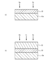
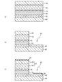
- 3A and 3B are cross-sectional views illustrating a film forming method of Comparative Example 1.
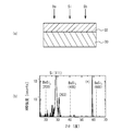
- FIG. 4A and FIG. 4B are cross-sectional views showing a film forming method of Comparative Example 2.
- FIG. 5A is a diagram showing an XRD diffraction pattern of the template BaSi layer 30 in FIG.
- FIG. 5B is a diagram showing an XRD diffraction pattern of the conductive BaSi layer 32 in FIG.
- FIG. 6A is a cross-sectional view illustrating a film forming method of Comparative Example 3.
- FIG. 6B is a diagram showing an XRD diffraction pattern of a sample formed by the method of Comparative Example 3.
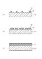
- FIG. 7A and FIG. 7B are diagrams showing a film forming method of Example 2.
- FIG. 8 is a diagram showing an XRD diffraction pattern of the conductive BaSi layer 32 formed by the method of Example 2.
- FIG. 9A is a cross-sectional view of a sample formed by the method of Example 2
- FIG. 9B is a cross-sectional view of a sample formed by the method of Comparative Example 4.
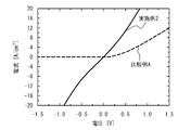
- FIG. 10 is a diagram showing current-voltage characteristics between the Si layer 10a and the conductive BaSi layer 32 of the sample formed by the method of Example 2 and the sample formed by the method of Comparative Example 4.
- FIG. 11A is a cross-sectional view of a sample formed by the method of Example 2.
- FIG. 11B is a diagram showing an XRD diffraction pattern of the second BaSi layer 18 formed by the method of the second embodiment.
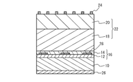
- 12 is a cross-sectional view of a solar cell manufactured using the method of Example 2.
- FIG. 13 is a cross-sectional view of the solar cell according to Example 3.
- FIG. 14A to FIG. 14C are cross-sectional views (part 1) illustrating the method for manufacturing the solar cell according to the third embodiment.
- FIG. 15A to FIG. 15C are cross-sectional views (part 2) illustrating the method for manufacturing the solar cell according to the third embodiment.
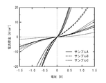
- FIG. 16 is a diagram showing current-voltage characteristics between the Si layers of Samples A to C and the conductive BaSi layer.
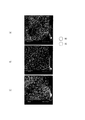
- FIGS. 17A to 17C are AFM images of the surface after forming the intermediate BsSi layers of samples A to C, respectively.
- 18 (a) to 18 (c) are views that are assumed to be cross sections of FIGS. 17 (a) to 17 (c), respectively.
- FIG. 19A and FIG. 19B are cross-sectional views of the solar cell according to Example 5.
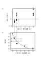
- FIG. 20A and FIG. 20B are diagrams showing the resistance and the aperture ratio with respect to the film thickness of the intermediate BaSi layer, respectively.
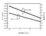
- FIG. 21 is a diagram showing conversion efficiency with respect to series resistance and Fill factor in a solar cell.
- FIG. 1 is a cross-sectional view of a solar cell according to Example 1.
- FIG. A tunnel junction layer 16 is formed on the Si layer 10 having the first conductivity type (for example, p-type).
- the Si layer 10 includes a dopant such as B (boron), Al (aluminum), and Ga (gallium).
- the dopant concentration of the Si layer 10 is preferably 1 ⁇ 10 16 to 1 ⁇ 10 18 cm ⁇ 3 , for example.
- a Si substrate having a film thickness of several hundred ⁇ m can be used.
- a Si thin film having a thickness of, for example, 50 to 500 nm formed on a glass substrate or the like can be used.
- the tunnel junction layer 16 includes a tunnel Si layer 12 and a tunnel BaSi layer 14.
- the tunnel Si layer 12 and the tunnel BaSi layer 14 form a tunnel junction.
- the tunnel Si layer 12 is formed on the Si layer 10 and has a first conductivity type (for example, p-type) having a dopant concentration higher than that of the Si layer 10.
- the tunnel Si layer 12 preferably has a dopant such as B or Al, and has a thickness of 10 to 50 nm and a dopant concentration of 1 ⁇ 10 19 to 1 ⁇ 10 20 cm ⁇ 3 , for example.
- the tunnel BaSi layer 14 is formed on the tunnel Si layer 12 and is of a second conductivity type (for example, n-type) having a dopant concentration higher than that of a second BaSi layer 18 described later.
- the tunnel BaSi layer 14 has a dopant such as Sb (antimony) or As (arsenic), for example, and has a film thickness of 10 to 50 nm and a dopant concentration of 1 ⁇ 10 19 to 1 ⁇ 10 20 cm ⁇ 3 , for example. Is preferred.
- a BaSi layer 22 having a pn junction is formed on the tunnel junction layer 16.
- the BaSi layer 22 includes a second conductivity type (for example, n-type) second BaSi layer 18 formed on the tunnel junction layer 16 and a first conductivity type (for example, p-type) first layer formed on the second BaSi layer 18.
- 1 BaSi layer 20 The first BaSi layer 20 and the second BaSi layer 18 form a pn junction.
- the second BaSi layer 18 has a dopant such as Sb or As, and preferably has a film thickness of 500 to 1000 nm and a dopant concentration of 1 ⁇ 10 16 to 5 ⁇ 10 16 cm ⁇ 3 , for example.
- the first BaSi layer 20 has a dopant such as Al, for example, and preferably has a film thickness of 50 to 100 nm and a dopant concentration of 5 ⁇ 10 17 to 5 ⁇ 10 18 cm ⁇ 3 , for example.
- a second electrode 24 for supplying carriers to the first BaSi layer 20 of the BaSi layer 22 is formed on the BaSi layer 22.
- the second electrode 24 is preferably made of a metal such as Al, for example, and preferably has an opening so that the light 50 can be transmitted.
- a first electrode 26 that supplies carriers to the Si layer 10 is formed under the Si layer 10.
- the first electrode 26 is preferably made of a metal such as Al.
- the tunnel BaSi layer 14, the second BaSi layer 18, the first BaSi layer 20, and the intermediate BaSi layer described in the second embodiment include Ba and Si, and are, for example, a barium silicide layer.
- the stoichiometric composition of barium silicide is BaSi 2 , but may be different from the stoichiometric composition.
- the tunnel BaSi layer 14, the second BaSi layer 18, the first BaSi layer 20, and the intermediate BaSi layer may contain, for example, Sr in addition to the barium silicide layer. That is, a mixed crystal of barium silicide and strontium silicide may be used.
- the energy band gap Eg is set to 1.4 eV by making the tunnel BaSi layer 14, the second BaSi layer 18, the first BaSi layer 20 and the intermediate BaSi layer, for example, Ba 0.5 Sr 0.5 Si 2 layers. Can do. Thereby, it is possible to provide a solar cell with higher efficiency and capable of being thinned.
- a mixed crystal of a silicide other than strontium silicide and barium silicide may be used.
- the tunnel BaSi layer 14, the second BaSi layer 18, the first BaSi layer 20, and the intermediate BaSi layer may contain a Group II element (that is, an alkaline earth metal element) such as Mg (magnesium) or Ca (calcium).
- a mixed crystal of magnesium silicide or calcium silicide and barium silicide may be used.
- an alkaline earth metal silicide containing at least barium silicide may be used.
- the tunnel BaSi layer 14, the second BaSi layer 18, the first BaSi layer 20, and the intermediate BaSi layer appropriately contain the elements exemplified above so as to have an energy band gap of 1.4 to 1.7 eV suitable for solar cells. It is preferable.
- FIG. 2 is an energy band diagram of a semiconductor layer in the solar cell according to Example 1.
- EF indicates the Fermi level.
- the Si layer 10 has an energy band gap Eg1
- the BaSi layer 22 has an energy band gap Eg2. Since the pn junction is formed by the BaSi layer 22 having a large band gap, it is possible to provide a solar cell that can be thinned with high efficiency.
- the tunnel Si layer 12 has a higher dopant concentration than the Si layer 10.
- the tunnel BaSi layer 14 has a higher dopant concentration than the second BaSi layer 18.
- the tunnel junction layer 16 can be formed by the tunnel Si layer 12 and the tunnel BaSi layer 14. Carriers can tunnel through the tunnel junction layer 16. Therefore, ohmic contact between the Si layer 10 and the second BaSi layer 18 is possible.
- a high-quality BaSi layer can be obtained by forming a BaSi layer on a (111) -oriented Si layer.
- the contact resistance between the Si layer 10 and the BaSi layer 22 is increased. This is because the electron affinity of the Si layer 10 is 4.0 eV and the electron affinity of the BaSi layer 22 is as small as 3.3 eV, and a barrier against carriers is formed between the Si layer 10 and the BaSi layer 22.
- a tunnel junction layer is formed between the Si layer 10 and the BaSi layer 22 having a pn junction.
- the electrical contact characteristic between the Si layer 10 and the BaSi layer 22 can be improved.
- the contact resistance between the Si layer 10 and the BaSi layer 22 can be reduced.
- the Si layer 10 and the tunnel Si layer 12 have the same conductivity type (first conductivity type), and the tunnel Si layer 12 preferably has a higher dopant concentration than the Si layer 10. .
- the second BaSi layer 18 and the tunnel BaSi layer 14 preferably have the same conductivity type (second conductivity type), and the tunnel BaSi layer 14 preferably has a higher dopant concentration than the second BaSi layer 18.
- the tunnel junction layer 16 is provided on the Si layer 10
- the tunnel Si layer 12 has the same conductivity type as the Si layer 10
- the tunnel BaSi layer 14 has a conductivity type different from that of the Si layer 10. Therefore, the second BaSi layer 18 having a conductivity type different from that of the Si layer 10 is formed on the tunnel BaSi layer 14, and the first BaSi layer 20 has the same conductivity type as that of the Si layer 10.
- a pn junction can be provided.
- the p-type is used as the first conductivity type and the n-type is used as the second conductivity type opposite to the first conductivity type.
- the first conductivity type is p-type and the second conductivity type is It may be n-type.
- the Si layer 10 becomes p-type. Therefore, when the Si layer 10 and the BaSi layer 22 having a pn junction are brought into contact with each other using a tunnel junction, the second BaSi layer 18 on the Si layer 10 side is made n-type, and the first BaSi layer 22 on the surface side is made p-type. preferable. Therefore, it is preferable that the first conductivity type is p-type and the second conductivity type is n-type.
- Example 2 is an example of a tunnel junction structure and a manufacturing method thereof according to Example 1.
- the tunnel Si layer 12 and the tunnel BaSi layer 14 are formed with a film thickness of, for example, about 50 nm or less, respectively.
- Example 2 is an example in which a thin and high-quality BaSi layer is formed on a Si layer.
- FIG. 3A and 3B are cross-sectional views illustrating a film forming method of Comparative Example 1.
- a Ba layer is formed on the (111) -oriented Si layer 10a by vapor deposition or the like.
- the substrate temperature is set to a temperature at which Si and Ba react to form barium silicide.
- the substrate temperature is set to 450 to 700 ° C.
- the Ba layer 33 and the Si layer 10a react to form the template BaSi layer 30.
- the template BaSi layer 30 is formed using the RDE (Reactive / Deposition / Epitaxy) method.
- a conductive BaSi layer 32 into which a dopant is introduced is formed on the template BaSi layer 30 by using MBE (Molecular Beam Epitaxy) method.
- Comparative Example 1 since the conductive BaSi layer 32 is formed using the template BaSi layer 30 as a template, a high-quality conductive BaSi layer 32 can be formed. However, the template BaSi layer 30 is not added with a dopant and has a thickness of about 20 nm. For this reason, the contact resistance between the conductive BaSi layer 32 and the Si layer 10a is increased. Further, in order to form a higher quality conductive BaSi layer 32, an undoped BaSi layer may be formed on the template BaSi layer 30 by using the MBE method, and the conductive BaSi layer 32 may be formed on the undoped BaSi layer. In this case, the contact resistance between the conductive BaSi layer 32 and the Si layer 10a is further increased. Therefore, as Comparative Example 2, the introduction of a dopant when forming the template BaSi layer 30 using the RDE method was examined.
- FIG. 4A and FIG. 4B are cross-sectional views showing a film forming method of Comparative Example 2.
- Si layer 10a a p-type Si wafer doped with B having (111) as the main surface was used.
- the hole concentration of the Si layer 10a is about 6 ⁇ 10 17 cm ⁇ 3 .
- Ba and Sb are vapor-deposited on the Si layer 10a.
- the substrate temperature is set to a temperature at which Ba reacts with Si.
- the template BaSi layer 30 is formed.
- the film forming conditions for the template BaSi layer 30 are as follows. Deposition method: RDE method
- Ba deposition rate 1.55 nm / min
- Sb cell temperature 250 ° C.
- Deposition time about 5 minutes
- Sb, Ba and Si were vapor-deposited on the template BaSi layer 30 by using the MBE method, and a conductive BaSi layer 32 using Sb as a dopant was formed.
- the film forming conditions for the conductive BaSi layer 32 are as follows. Deposition method: MBE method Substrate temperature: 550 ° C. Ba deposition rate: 2.6 nm / min Si deposition rate: 1.55 nm / min Sb cell temperature: 250 ° C. Film formation time: about 60 minutes By setting the Sb cell temperature to 250 ° C., an electron concentration of about 10 20 cm ⁇ 3 can be obtained as the conductive BaSi layer 32 of Example 2 described later.
- FIG. 5A is a diagram showing an XRD (X-ray diffraction method) diffraction pattern of the template BaSi layer 30 in FIG.
- peaks corresponding to the (111) plane of Si are observed, but peaks of the (200), (400), and (600) planes of BaSi 2 are not observed. From this, it was found that the template BaSi layer 30 was not a good crystal. Note that the peak indicated by (*) was observed at the position of the Si (222) plane, but this peak (*) is a peak reflected by the crystal plane a plurality of times, and the peak of the Si (222) plane. is not.
- FIG. 5A is a diagram showing an XRD (X-ray diffraction method) diffraction pattern of the template BaSi layer 30 in FIG.
- peaks corresponding to the (111) plane of Si are observed, but peaks of the (200), (400), and (600) planes of BaSi 2 are not observed. From this, it was found that the
- 5B is a diagram showing an XRD diffraction pattern of the conductive BaSi layer 32 in FIG. As shown in FIG. 5A, peaks corresponding to the (111) plane of Si are observed, but peaks of the (200), (400), and (600) planes of BaSi 2 are not observed. This shows that the conductive BaSi layer 32 is not a good crystal.
- Comparative Example 2 it was found that when the dopant was introduced into the template BaSi layer 30 using the RDE method, the crystallinity of the template BaSi layer 30 and the conductive BaSi layer 32 deteriorated. Therefore, as Comparative Example 3, it was studied to directly form a conductive BaSi layer on the Si layer 10a using the MBE method.
- FIG. 6A is a cross-sectional view illustrating a film forming method of Comparative Example 3.
- MBE MBE method
- FIG. 6B is a diagram showing an XRD diffraction pattern of a sample formed by the method of Comparative Example 3. As shown in FIG. 6B, peaks corresponding to the (111) plane of Si are observed, but peaks of the (200), (400), and (600) planes of BaSi 2 are not observed. From this, it was found that also in Comparative Example 3, the conductive BaSi layer 32 was not a good crystal.
- FIG. 7A and FIG. 7B are diagrams showing a film forming method of Example 2.
- FIG. 7A Ba was deposited very thinly on the same Si layer 10a as in Comparative Example 2.
- the substrate temperature is set to a temperature at which Ba reacts with Si.
- the intermediate BaSi layer 28 is formed.
- the film forming conditions for the intermediate BaSi layer 28 are as follows. Deposition method: RDE method Substrate temperature: 550 ° C Ba film formation rate: 1.55 nm / min Film formation time: about 0.5 minutes Since the deposition amount of Ba is very small, Ba does not cover the entire surface of the Si layer 10a. Therefore, an intermediate BaSi layer 28 including Ba and Si is formed on the Si layer 10a, having an opening 29 that exposes the surface of the Si layer 10a.
- the conductive BaSi layer 32 was formed so as to cover the intermediate BaSi layer 28 and to be in contact with the Si layer 10a through the opening 29.
- the film forming conditions for the conductive BaSi layer 32 are as follows. Deposition method: MBE method Substrate temperature: 550 ° C. Ba deposition rate: 2.6 nm / min Si deposition rate: 1.55 nm / min Sb cell temperature: 250 ° C. Deposition time: about 60 minutes As described above, Sb can be simultaneously formed to introduce Sb as a dopant into the conductive BaSi layer 32.
- FIG. 8 is a diagram showing an XRD diffraction pattern of the conductive BaSi layer 32 formed by the method of Example 2.
- FIG. BaSi 2 peaks at (200), (400) and (600) planes are observed. This indicates that an ⁇ -axis oriented BaSi 2 layer is formed on the (111) -oriented Si layer.
- the conductive BaSi layer 32 having good crystallinity could be formed.
- FIG. 9A is a cross-sectional view of a sample formed by the method of Example 2
- FIG. 9B is a cross-sectional view of a sample formed by the method of Comparative Example 4.
- the high-concentration Si layer 12a is formed on the p-type Si layer 10a, and the intermediate BaSi layer 28, which is the same as that shown in FIGS.
- An n-type conductive BaSi layer 32 is formed on the BaSi layer 28.
- the Si layer 10a is a B-doped (111) substrate having a hole concentration of about 6 ⁇ 10 17 cm ⁇ 3 .
- the film forming conditions for the high-concentration Si layer 12a are as follows. Film formation method: MBE substrate temperature: 700 ° C. Dopants: B, Si and HBO 3 are simultaneously deposited. The high concentration Si layer 12a has a hole concentration of about 5 ⁇ 10 19 cm ⁇ 3 and a film thickness of 70 nm.
- the method for forming the intermediate BaSi layer 28 is the same as that in the first embodiment.
- the substrate temperature, the deposition rate of Ba and Si, and the Sb cell temperature during the formation of the conductive BaSi layer 32 are the same as in FIG.
- the film formation time of the conductive BaSi layer 32 was set so that the film thickness was 140 nm.
- Table 1 is a table showing the dopant, conductivity type, carrier concentration, and film thickness of each layer of the sample prepared by the method of Example 2.
- the film thickness of the intermediate BaSi layer 28 is a film thickness estimated from the film formation time.
- the template BaSi layer 30 is formed on the Si layer 10a, the undoped BaSi layer 35 is formed on the template BaSi layer 30, and the conductive BaSi layer 32 is formed on the undoped BaSi layer 35.
- the Si layer 10a is a B-doped (111) substrate having a hole concentration of about 6 ⁇ 10 17 cm ⁇ 3 .
- the film forming conditions for the template BaSi layer 30 are as follows. Deposition method: RDE method
- Ba film formation rate 1.55 nm / min
- Film formation time set so that film thickness is 20 nm
- the method for forming the undoped BaSi layer 35 is as follows. Deposition method: MBE method Substrate temperature: 550 ° C. Ba film formation rate: 2.6 nm / min Si film formation rate: 1.55 nm / min Film formation time: about 60 minutes The undoped BaSi layer 35 is not intentionally doped, but in the Hall effect measurement, electrons are used. The concentration is about 10 16 cm ⁇ 3 .
- the film forming conditions for the conductive BaSi layer 32 are as follows. Deposition method: MBE method Substrate temperature: 550 ° C. Ba deposition rate: 2.6 nm / min Si deposition rate: 1.55 nm / min Sb cell temperature: 250 ° C. Deposition time: about 60 minutes
- Table 2 is a table showing the dopant, conductivity type, carrier concentration and film thickness of each layer of the sample produced by the method of Comparative Example 4.
- FIG. 10 shows the relationship between the Si layer 10a and the conductive BaSi layer 32 of the sample of FIG. 9A formed by the method of Example 2 and the sample of FIG. 9B formed by the method of Comparative Example 4. It is the figure which showed the current-voltage characteristic between. As shown in FIG. 10, in Comparative Example 4, the current-voltage characteristic is a rectifying characteristic. On the other hand, in Example 2, ohmic characteristics are obtained. Thus, in Example 2, the current flowing through the tunnel junction layer 16 exhibited ohmic characteristics, and good contact characteristics could be obtained between the conductive BaSi layer 32 and the Si layer 10a.
- FIG. 11A is a cross-sectional view of a sample formed by the method of Example 2.
- the tunnel Si layer 12 is formed on the p-type Si layer 10
- the intermediate BaSi layer 28 is formed on the tunnel Si layer 12
- the tunnel BaSi layer 14 is formed on the intermediate BaSi layer 28
- the second BaSi layer is formed on the tunnel BaSi layer 14.
- Layer 18 is formed.
- the Si layer 10 is a B-doped (111) substrate having a hole concentration of about 6 ⁇ 10 17 cm ⁇ 3 .
- the tunnel Si layer 12 has B as a dopant, a hole concentration of about 5 ⁇ 10 19 cm ⁇ 3 , and a film thickness of 70 nm.
- the conditions for forming the tunnel Si layer 12 are the same as those for the high-concentration Si layer 12a shown in FIG.
- the intermediate BaSi layer 28 has a thickness of about 1 nm.
- the film forming conditions for the intermediate BaSi layer 28 are the same as those in FIG.
- the tunnel BaSi layer 14 has Sb as a dopant, an electron concentration of about 10 20 cm ⁇ 3 , and a film thickness of 140 nm.
- the film forming conditions of the tunnel BaSi layer 14 are the same as those of the conductive BaSi layer 32 in FIG.
- the second BaSi layer 18 is not intentionally doped, but has an electron concentration of about 10 16 cm ⁇ 3 and a film thickness of 520 nm.
- the film forming conditions for the second BaSi layer 18 are as follows. Deposition method: MBE method Substrate temperature: 550 ° C. Ba deposition rate: 2.6 nm / min Si deposition rate is 1.55 nm / min Growth time: 60 minutes
- FIG. 11B is a diagram showing an XRD diffraction pattern of the second BaSi layer 18 formed by the method of the second embodiment. As shown in FIG. 11 (b), peaks on the (200), (400) and (600) planes of BaSi 2 are observed. As described above, in Example 2, the second BaSi layer 18 having good crystallinity could be formed.
- FIG. 12 is a cross-sectional view of a solar cell manufactured by the method of Example 2.
- an intermediate BaSi layer 28 having an opening is formed on the tunnel Si layer 12 as compared with Example 1.
- Other structures are the same as those of the first embodiment, and a description thereof is omitted.
- the solar cell manufactured by the method of Example 2 is manufactured as follows, for example.
- a first BaSi layer 20 is formed on the second BaSi layer 18 of FIG.
- a second electrode 24 is formed on the first BaSi layer 20.
- a first electrode 26 is formed under the Si layer 10.
- an opening that exposes the surface of the tunnel Si layer 12 on the tunnel Si layer 12 in FIG. 12 (corresponding to the Si layer 10a in FIG. 7A).
- An intermediate BaSi layer 28 having 29 is formed.
- no dopant is added to the intermediate BaSi layer 28.
- the intermediate BaSi layer 28 which is ⁇ -axis oriented can be formed on the Si layer 10a.
- the tunnel BaSi layer 14 in FIG. 12 (corresponding to the conductive BaSi layer 32 in FIG. 7B) covers the intermediate BaSi layer 28 and is in contact with the Si layer 10a through the opening 29. To form. At this time.
- the tunnel BaSi layer 14 also grows in the lateral direction so as to close the opening 29.
- the tunnel BaSi layer 14 having good crystallinity is formed using the intermediate BaSi layer 28 as a template.
- an intermediate BaSi layer 28 having an opening 29 in which the tunnel Si layer 12 and the tunnel BaSi layer 14 are in direct contact is formed at the interface between the tunnel Si layer 12 and the tunnel BaSi layer 14. Therefore, since the tunnel BaSi layer 14 directly contacts the tunnel Si layer 12 through the opening 29, the contact characteristics between the tunnel Si layer 12 and the tunnel BaSi layer 14 can be improved as shown in FIG.
- the intermediate BaSi layer 28 only needs to have a lower dopant concentration than the conductive BaSi layer 32.
- the opening 29 may be a hole penetrating the intermediate BaSi layer 28, or may be a space between a plurality of BaSi formed in an island shape.
- an intermediate BaSi layer 28 by depositing Ba on the tunnel Si layer 12 in FIG. 12 and reacting Ba with the tunnel Si layer 12.
- the temperature for reacting Ba and Si is preferably 450 ° C. to 700 ° C.
- the substrate temperature is set to a temperature at which Ba reacts with Si when Ba27 is deposited on the tunnel Si layer 12 in order to form the intermediate BaSi layer 28.
- the substrate temperature may be raised after Ba is deposited, and Ba may react with Si.
- Sb is used as the n-type dopant, but As or the like may be used.
- B is used as the p-type dopant, Al or the like may be used.
- the BaSi layer may contain a group II element such as Sr (that is, an alkaline earth metal element).
- FIG. 13 is a cross-sectional view of the solar cell according to Example 3.
- a conductive layer 42 is formed on the insulating substrate 40.
- a Si layer 10 is formed on the conductive layer 42.
- a first electrode 26 is formed on the conductive layer 42.
- Other structures are the same as those of the first embodiment or the second embodiment, and the description thereof is omitted.
- the insulating substrate 40 for example, a glass substrate, a silicon oxide substrate such as SiO 2 , or another insulating substrate can be used.
- a metal layer such as ZnO (zinc acid) to which Al is added can be used.
- the film thickness of the conductive layer 42 can be set to, for example, 500 to 1000 nm.
- the Si layer 10 is, for example, a (111) -oriented polycrystalline Si layer or a single-crystal Si layer, and the film thickness can be, for example, 50 to 500 nm.
- a conductive layer 42 that is a ZnO layer doped with Al is formed on an insulating substrate 40 that is a SiO 2 substrate.
- An Al layer 44 is formed on the conductive layer 42.
- An amorphous Si layer 46 is formed on the Al layer 44.
- the amorphous Si layer 46 and the Al layer 44 are exchanged by heating at 500 ° C. for about 10 hours in a nitrogen atmosphere. By this treatment, the conductive layer 42 is not altered.
- the (111) -oriented polycrystalline Si layer 10 is formed on the conductive layer 42.
- An Al layer 48 is formed on the Si layer 10. As shown in FIG. 14C, the Al layer 48 is removed.
- the tunnel junction layer 16, the second BaSi layer 18, and the first BaSi layer 20 are formed on the Si layer 10 in the same manner as in the first or second embodiment.
- the first BaSi layer 20 to the Si layer 10 are selectively removed to form an opening 52.
- the first electrode 26 is formed on the conductive layer 42 on the bottom surface of the opening 52.
- a second electrode 24 is formed on the first BaSi layer 20.
- Example 3 a conductive layer 42 is provided between the insulating substrate 40 and the Si layer 10, and the first electrode 26 supplies carriers to the Si layer 10 through the conductive layer 42. Accordingly, even when the Si layer 10 is formed on the insulating substrate 40 as in Non-Patent Document 1, the first electrode 26 that supplies carriers to the Si layer 10 can be easily formed.
- Example 4 is an example in which the film thickness of the intermediate BaSi layer is changed in FIGS. 7A and 7B of Example 2.
- FIG. The deposition times of the intermediate BaSi layer 28 in samples A to C were 0.5 minutes, 1 minute, and 5 minutes, respectively.
- the film thickness of the intermediate BaSi layer 28 calculated from the film forming speeds in the samples A to C corresponds to 1, 2, and 10 nm.
- Other film forming conditions are the same as those in FIGS. 7A and 7B.
- Table 3 summarizes the conditions of samples A to C.
- FIG. 16 is a diagram showing current-voltage characteristics between the Si layer 10a and the conductive BaSi layer 32 of samples A to C.
- the solid line is the measurement result of sample A
- the broken line is the measurement result of sample B
- the dotted line is the measurement result of sample C.
- the plurality of curves for each of samples A to C are the results of measuring a plurality of samples.
- the voltage-current characteristic of sample A is close to the ohmic characteristic.
- the voltage-current characteristics of sample B are close to ohmic characteristics, but the resistance is higher than that of sample A.
- the resistance of the voltage-current characteristic of sample C is further increased.
- FIGS. 17 (a) to 17 (c) are AFM (Atomic Force Microscope) images of the surface after the intermediate BsSi layer 28 of samples A to C is formed (the state of FIG. 7 (a)), respectively.
- 18 (a) to 18 (c) are views that are assumed to be cross sections of FIGS. 17 (a) to 17 (c), respectively.
- FIG. 17A regions where the contrast changes abruptly are scattered. This region is considered to be an island 90 of BaSi.
- the black linear region 92 is considered as a step of the Si substrate.
- FIG. 18A in sample A, it is considered that the cores of the intermediate BaSi layer 28 are scattered as islands 90 on the high-concentration Si layer 12a.
- the density of the region considered to be the BaSi island 90 is increased, and there are also places where the islands 90 are in contact with each other.
- FIG. 18B in sample B, lateral growth starts from the nucleus of the intermediate BaSi layer 28 on the high-concentration Si layer 12a, the island-like high-concentration Si layer 12a becomes large, and islands It is thought that they are in contact with each other and growing into larger islands. In this state, the opening between the intermediate BaSi layers 28 is reduced. For this reason, when the conductive BaSi layer 32 is formed, the area in which the high-concentration Si layer 12a and the conductive BaSi layer 32 are in direct contact with each other is smaller than that in FIG. For this reason, as shown by the broken line in FIG.
- FIG. 17 (c) a region considered to be an island of BaSi is hardly observed.
- FIG. 18C in the sample C, it is considered that the intermediate BaSi layer 28 on the high concentration Si layer 12a is continuous in the lateral direction. In this state, the non-doped intermediate BaSi layer 28 is continuously formed between the high-concentration Si layer 12a and the conductive BaSi layer 32. If the film formation time of the intermediate BaSi layer 28 is lengthened, the film thickness of the intermediate BaSi layer 28 is increased. Therefore, the resistance of the sample C increases as shown by the dotted line in FIG.
- the film formation time of the intermediate BaSi layer 28 in the step of forming the intermediate BaSi layer 28 in FIG. 7A is the film thickness of the intermediate BaSi layer 28 in terms of film formation speed. Is preferably a time of 2 nm or less. More preferably, it is 1 nm or less.
- Example 5 is an example of a tandem solar cell.
- FIG. 19A and FIG. 19B are cross-sectional views of the solar cell according to Example 5.
- the Si layer 10 includes an n-type second Si layer 64 and a p-type first Si layer 62 formed on the n-type second Si layer 64.
- the tunnel junction layer 16 and the BaSi layer 22 similar to those in the first to fourth embodiments are formed.
- the tunnel junction layer 16 has a p-type tunnel Si layer 12 formed on the p-type first Si layer 62 and an n-type tunnel BaSi layer 14 formed on the tunnel Si layer 12.
- the BaSi layer 22 includes an n-type second BaSi layer 18 formed on the tunnel BaSi layer 14 and a p-type first BaSi layer 20 formed on the second BaSi layer 18.
- a second electrode 24 to which carriers are supplied from the first BaSi layer 20 of the BaSi layer 22 is formed on the BaSi layer 22.
- a first electrode 26 to which carriers are supplied from the Si layer 10 is formed under the second Si layer 64 of the Si layer 10.
- the film thickness of the Si layer 10 is, for example, 50 ⁇ m to 200 ⁇ m, and the film thickness of the BaSi layer 22 is, for example, 1 ⁇ m to 2 ⁇ m.
- the Si layer 10b has a p-type second Si layer 64b and an n-type first Si layer 62b formed on the p-type second Si layer 64b.
- a tunnel junction layer 16b and a BaSi layer 22b similar to those in the first to fourth embodiments are formed on the n-type first Si layer 62b.
- the tunnel junction layer 16b has an n-type tunnel Si layer 12b formed on the n-type first Si layer 62b and a p-type tunnel BaSi layer 14b formed on the tunnel Si layer 12b.
- the BaSi layer 22b has a p-type second BaSi layer 18b formed on the tunnel BaSi layer 14b and an n-type first BaSi layer 20b formed on the second BaSi layer 18b.
- the same intermediate BaSi layer 28 as in the second to fourth embodiments may be formed between the tunnel Si layer 12 and the tunnel BaSi layer 14.
- the Si layer 10 has a pn junction. Thereby, a photovoltaic force is generated also in the Si layer 10 and can function as a solar cell.
- the BaSi layer 22 has a larger band gap than Si. Therefore, light having a short wavelength is converted into electric energy by the BaSi layer 22, and light having a long wavelength is converted into electric energy by the Si layer. Thereby, a solar cell with high photoelectric efficiency is realizable.
- the first Si layer 62 preferably has the same conductivity type as the tunnel Si layer 12 so that no pn junction is interposed between the first Si layer 62 and the tunnel Si layer 12. That is, when the second Si layer 64 is of the second conductivity type and the first Si layer 62 is of the first conductivity type, the second BaSi layer 18 is of the second conductivity type, and the first BaSi layer 20 is of the first conductivity type. It is preferable.
- Example 6 is an example in which a preferable aperture ratio range was obtained from the results of Example 4.
- FIGS. 20A and 20B are diagrams showing the resistance and the aperture ratio with respect to the film thickness of the intermediate BaSi layer 28, respectively.
- the vertical axis represents the resistance per unit cross-sectional area obtained from the voltage-current characteristics of FIG. The resistance value was calculated from the current density when a voltage of 0.1 V was applied.
- the plots when the film thickness of the intermediate BaSi layer 28 is 1, 2, and 10 nm correspond to the samples A, B, and C in Example 4, respectively.
- FIG. 20B shows the aperture ratio obtained from FIGS. 17A to 17C.
- an uncovered region between the covering portion and the covering portion of the intermediate BaSi layer 28 covering the high-concentration Si layer 12a is defined as an opening.
- the aperture ratio indicates the area of the opening with respect to the entire area.
- a sample with an intermediate BaSi layer 28 having a thickness of 0 nm (no intermediate BaSi layer 28 is formed) and a sample with 6 nm are prepared. The aperture ratio was measured.
- the growth of the intermediate BaSi layer 28 is not a step flow growth but an island growth.
- the island is considered as a cone having a bottom radius R and a height H.
- the volume V of the intermediate BaSi layer 28 is expressed by the following equation.
- V (1/3) ⁇ R 2 HN Since the volume V of the intermediate BaSi layer 28 is proportional to the supply amount of Ba, it is proportional to time. Therefore, the proportionality constant C and time t are expressed by the following equation.
- FIG. 21 is a diagram showing conversion efficiency and fill factor with respect to series resistance in a solar cell.
- FIG. 21 shows the conversion efficiency and the fill factor of a general solar cell based on the inventor's experience. As shown in FIG. 21, the conversion efficiency and the fill factor deteriorate as the series resistance increases. In the example of FIG. 21, when the series resistance is 1 ⁇ cm 2 , the conversion efficiency deteriorates by about 2%. Thus, it is better that the series resistance is small.
- the series resistance in a semiconductor device including a solar cell is greatly affected by the contact resistance between the semiconductor and the electrode and the resistance of the semiconductor itself. For example, the contact resistance between the semiconductor and the electrode and the resistance of the semiconductor itself are about 1 ⁇ cm 2 .
- the silicon layer and the silicide layer contact resistance between is preferably from 1 .OMEGA.cm 2 1 order of magnitude smaller 0.1? cm 2 or less.
- the resistance in Sample B is approximately 0.1 ⁇ cm 2 . Therefore, from FIG. 20B, the aperture ratio is preferably 0.5 or more. Furthermore, in order to further reduce the contact resistance between the silicon layer and the silicide layer, the resistance is preferably 0.03 ⁇ cm 2 as in Sample A in FIG. Therefore, from FIG. 20B, the aperture ratio is preferably 0.7 or more.
- the aperture ratio is 1, no intermediate BaSi layer 28 is formed on the high-concentration Si layer 12a. For this reason, the crystallinity of the high-concentration BaSi layer 32 is deteriorated as shown in FIG. On the other hand, if a small amount of the intermediate BaSi layer 28 is formed on the high-concentration Si layer 12a, the high-concentration BaSi layer 32 is formed with good crystallinity around the island of the intermediate BaSi layer 28 as a nucleus. Therefore, the aperture ratio is preferably less than 1.
- the intermediate silicide layer (for example, intermediate BaSi layer 28) containing barium silicide is on the silicon layer (for example, high-concentration Si layer 12a). And has an opening.
- An upper silicide layer (for example, high-concentration BaSi layer 32) having a dopant concentration higher than that of the intermediate silicide layer and containing barium silicide is provided so as to cover the intermediate silicide layer and to be in contact with the silicon layer through the opening. Thereby, good electrical contact can be obtained between the silicon layer and the upper silicide layer.
- the opening ratio of the opening of the intermediate silicide layer is preferably 0.5 or more and less than 1, more preferably 0.7 or more and less than 1.
- the silicon layer preferably has a higher dopant concentration than the intermediate silicide layer. Further, since the silicon layer and the upper silicon layer form a tunnel junction layer, it is preferable that the silicon layer and the upper silicide layer have different conductivity types.
- solar cells have been described as an example of a semiconductor device.
- a transistor or the like may be used as long as it is a semiconductor device in which a silicide layer is formed on a silicon layer.
- the intermediate silicide layer As a method for forming the intermediate silicide layer, a method for forming the intermediate silicide layer by depositing barium on the silicon layer and reacting the barium with the silicon layer.
- a method of forming the upper silicide layer in FIG. 7B a method of forming the upper silicide layer by simultaneously depositing dopant, silicon and barium on the intermediate silicide layer and the silicon layer has been described.
- the intermediate silicide layer and the upper silicide layer may be formed by sputtering or CVD (Chemical Vapor Deposition).
- the solar cell includes a silicon layer (for example, Si layer 10), a tunnel junction layer formed on the silicon layer, and a silicide layer (barium silicide containing barium silicide) formed on the tunnel junction layer.
- a silicon layer for example, Si layer 10
- a tunnel junction layer formed on the silicon layer
- a silicide layer barium silicide containing barium silicide
- a pn junction made of a BaSi layer 22.
- the tunnel junction layer has a tunnel silicon layer (for example, tunnel Si layer 12) having a higher dopant concentration than the silicon layer and having the same conductivity type (first conductivity type) as the silicon layer, It is preferable to include a tunnel silicide layer (for example, tunnel BaSi layer 14) formed on the silicon layer and having a conductivity type opposite to the first conductivity type (second conductivity type) and containing barium silicide.
- a tunnel silicon layer for example, tunnel Si layer 12
- tunnel Si layer 12 having a higher dopant concentration than the silicon layer and having the same conductivity type (first conductivity type) as the silicon layer
- a tunnel silicide layer for example, tunnel BaSi layer 14
- the tunnel junction layer is a silicide layer formed on the tunnel junction layer and having a second conductivity type having a dopant concentration lower than that of the tunnel silicide layer and containing barium silicide (for example, the second BaSi layer 18); And a first silicide layer (first BaSi layer) which is formed on the two silicide layers and has the first conductivity type and contains barium silicide.
- the silicide layer is preferably made of barium silicide (for example, formed as a barium silicide crystal within a range including impurities such as dopants). Further, in order to improve the conversion efficiency of the solar cell, it is preferably made of strontium barium silicide (for example, formed as a crystal as strium barium silicide within a range including impurities such as dopants).
Landscapes
- Photovoltaic Devices (AREA)
- Electrodes Of Semiconductors (AREA)
Abstract
Description
テンプレートBaSi層30の成膜条件は以下である。
成膜方法:RDE法
基板温度:550℃
Baの成膜速度:1.55nm/分
Sbセル温度:250℃
成膜時間:約5分
導電性BaSi層32の成膜条件は以下である。
成膜方法:MBE法
基板温度:550℃
Baの成膜速度:2.6nm/分
Siの成膜速度:1.55nm/分
Sbセル温度:250℃
成膜時間:約60分
なお、Sbセル温度を250℃とすることにより、後述する実施例2の導電性BaSi層32として、1020cm-3程度の電子濃度が得られる。
導電性BaSi層32の成膜条件は以下である。
成膜方法:MBE法
基板温度:550℃
Baの成膜速度:2.6nm/分
Siの成膜速度:1.55nm/分
Sbセル温度:250℃
成膜時間:約60分
中間BaSi層28の成膜条件は以下である。
成膜方法:RDE法
基板温度:550℃
Baの成膜速度:1.55nm/分
成膜時間:約0.5分
Baの蒸着量は非常に小さいため、Baは、Si層10aの表面の全体を覆わない。よって、Si層10a上に、Si層10aの表面が露出するような開口29を有し、BaとSiとを含む中間BaSi層28が形成される。
導電性BaSi層32の成膜条件は以下である。
成膜方法:MBE法
基板温度:550℃
Baの成膜速度:2.6nm/分
Siの成膜速度:1.55nm/分
Sbセル温度:250℃
成膜時間:約60分
このように、Sbも同時の成膜することによりSbをドーパントとして、導電性BaSi層32に導入することができる。
高濃度Si層12aの成膜条件は以下である。
成膜方法:MBE法
基板温度:700℃
ドーパント:B、SiとHBO3を同時に蒸着
高濃度Si層12aのホール濃度は約5×1019cm-3、膜厚は70nmである。
中間BaSi層28の成膜方法は、実施例1と同じである。導電性BaSi層32の成膜の際の基板温度、BaおよびSiの成膜速度、Sbセル温度は図7(b)と同じである。導電性BaSi層32の成膜時間は膜厚が140nmとなるように設定した。表1は、実施例2の方法で作製した試料の各層のドーパント、導電型、キャリア濃度および膜厚を示す表である。なお、中間BaSi層28の膜厚は、成膜時間から推定した膜厚である。

テンプレートBaSi層30の成膜条件は以下である。
成膜方法:RDE法
基板温度:550℃
Baの成膜速度:1.55nm/分
成膜時間:膜厚が20nmとなるように設定
成膜方法:MBE法
基板温度:550℃
Baの成膜速度:2.6nm/分
Siの成膜速度:1.55nm/分
成膜時間:約60分
アンドープBaSi層35には意図的にはドープしていないが、ホール効果測定では電子濃度が約1016cm-3である。
成膜方法:MBE法
基板温度:550℃
Baの成膜速度:2.6nm/分
Siの成膜速度:1.55nm/分
Sbのセル温度:250℃
成膜時間:約60分

第2BaSi層18の成膜条件は以下である。
成膜方法:MBE法
基板温度:550℃
Baの成膜速度:2.6nm/分
Siの成膜速度が1.55nm/分
成長時間:60分

このとき1つの島の体積Viは次式で表される。
Vi=(1/3)πR2H
島の数Nのとき中間BaSi層28の体積Vは次式で表される。
V=(1/3)πR2HN
中間BaSi層28の体積Vは、Baの供給量に比例するため時間に比例する。よって、比例定数C、時間tとし、次式で表される。
V=Ct=(1/3)πR2HN
よって、
NR2∝t/H(t)
である。
また、中間BaSi層28の島の高さは、BaのSiへの拡散(またはSiのBaの拡散)に依存する。よって、結晶成長における原子の拡散モデルから次式で表される。
H∝√t
中間BaSi層28の島がシリコン層表面を覆う割合(1-開口率)はNR2で表される。よって、
(1-開口率)=NR2∝√t∝√(中間BaSi層28の膜厚)
となる。
図20(b)の破線は、実験値(黒丸)に合うように上記モデル式を用いて描いた曲線である。
Claims (14)
- シリコン層と、
前記シリコン層上に設けられ、開口を有し、バリウムシリサイドを含む中間シリサイド層と、
中間シリサイド層を覆い、前記開口を介しシリコン層に接するように設けられ、前記中間シリサイド層よりドーパント濃度が高くバリウムシリサイドを含む上部シリサイド層と、
を含む半導体装置。 - 前記開口の開口率は、0.5以上1未満である請求項1記載の半導体装置。
- 前記シリコン層は、前記中間シリサイド層よりドーパント濃度が高い請求項1または2記載の半導体装置。
- 前記シリコン層と前記上部シリサイド層とは、異なる導電型である請求項1から3のいずれか一項記載の半導体装置。
- 前記シリコン層と前記上部シリサイド層とはトンネル接合を形成する請求項4記載の半導体装置。
- 前記中間シリサイド層および前記上部シリサイド層は、バリウムシリサイドからなる請求項1から5のいずれか一項記載の半導体装置。
- シリコン層上に、前記シリコン層の表面が露出するような開口を有し、バリウムシリサイドを含む中間シリサイド層を形成する工程と、
中間シリサイド層を覆い、前記開口を介しシリコン層に接するように、前記中間シリサイド層よりドーパント濃度が高くバリウムシリサイドを含む上部シリサイド層を形成する工程と、
を含み、
前記中間シリサイド層を形成する工程は、前記シリコン層上にバリウムを堆積させ、前記バリウムを前記シリコン層と反応させることにより前記中間シリサイド層を形成する工程である半導体装置の製造方法。 - 前記上部シリサイド層を形成する工程は、前記中間シリサイド層上および前記シリコン層上にドーパント、シリコンおよびバリウムを同時に蒸着することにより前記上部シリサイド層を形成する工程である請求項7記載の半導体装置の製造方法。
- シリコン層と、
前記シリコン層上に形成されたトンネル接合層と、
前記トンネル接合層上に形成され、バリウムシリサイドを含むシリサイド層からなるpn接合と、前記シリコン層からキャリアが供給される第1電極と、
前記シリサイド層からキャリアが供給される第2電極と、
を具備する太陽電池。 - 前記シリコン層は第1導電型であり、
前記トンネル接合層は、前記シリコン層上に形成された前記シリコン層よりドーパント濃度の高い前記第1導電型であるトンネルシリコン層と、前記トンネルシリコン層上に形成され前記第1導電型の反対の導電型である第2導電型でありバリウムシリサイドを含むトンネルシリサイド層と、を含み、
前記シリサイド層は、前記トンネル接合層上に形成され前記トンネルシリサイド層よりドーパント濃度が低い前記第2導電型でありバリウムシリサイドを含む第2シリサイド層と、前記第2シリサイド層上に形成され前記第1導電型でありバリウムシリサイドを含む第1シリサイド層と、を含む請求項9記載の太陽電池。 - 前記トンネルシリコン層と前記トンネルシリサイド層との界面に形成され、前記トンネルシリコン層と前記トンネルシリサイド層とが直接接するような開口を有し、前記トンネルシリサイド層よりドーパント濃度の低く、バリウムシリサイドを含む中間シリサイド層を具備する請求項10記載の太陽電池。
- 前記開口の開口率は、0.5以上1未満である請求項11記載の太陽電池。
- 前記シリサイド層は、バリウムシリサイドからなる請求項9から12のいずれか一項記載の太陽電池。
- 前記シリサイド層は、ストロンチウムバリウムシリサイドからなる請求項9から12のいずれか一項記載の太陽電池。
Priority Applications (3)
| Application Number | Priority Date | Filing Date | Title |
|---|---|---|---|
| US13/318,913 US8502191B2 (en) | 2009-05-12 | 2010-05-11 | Semiconductor device, manufacturing method therefor, and solar cell |
| CN201080020824.5A CN102422438B (zh) | 2009-05-12 | 2010-05-11 | 半导体装置及其制造方法以及太阳能电池 |
| JP2011513338A JP5550025B2 (ja) | 2009-05-12 | 2010-05-11 | 半導体装置およびその製造方法並びに太陽電池 |
Applications Claiming Priority (4)
| Application Number | Priority Date | Filing Date | Title |
|---|---|---|---|
| JP2009115337 | 2009-05-12 | ||
| JP2009-115337 | 2009-05-12 | ||
| JP2009185666 | 2009-08-10 | ||
| JP2009-185666 | 2009-08-10 |
Publications (1)
| Publication Number | Publication Date |
|---|---|
| WO2010131639A1 true WO2010131639A1 (ja) | 2010-11-18 |
Family
ID=43085011
Family Applications (1)
| Application Number | Title | Priority Date | Filing Date |
|---|---|---|---|
| PCT/JP2010/057936 Ceased WO2010131639A1 (ja) | 2009-05-12 | 2010-05-11 | 半導体装置およびその製造方法並びに太陽電池 |
Country Status (5)
| Country | Link |
|---|---|
| US (1) | US8502191B2 (ja) |
| JP (1) | JP5550025B2 (ja) |
| CN (1) | CN102422438B (ja) |
| TW (1) | TWI407575B (ja) |
| WO (1) | WO2010131639A1 (ja) |
Cited By (9)
| Publication number | Priority date | Publication date | Assignee | Title |
|---|---|---|---|---|
| WO2014171146A1 (ja) * | 2013-04-18 | 2014-10-23 | 株式会社 東芝 | 太陽光発電モジュール |
| WO2015129878A1 (ja) * | 2014-02-27 | 2015-09-03 | 東ソー株式会社 | 珪化バリウム系バルク体、膜及びその製造方法 |
| JP2015160998A (ja) * | 2014-02-27 | 2015-09-07 | 東ソー株式会社 | 珪化バリウム膜およびその製造方法 |
| JP2015220371A (ja) * | 2014-05-19 | 2015-12-07 | 国立大学法人 筑波大学 | 半導体装置およびその製造方法 |
| JP2015221744A (ja) * | 2014-04-30 | 2015-12-10 | 東ソー株式会社 | 珪化バリウム系バルク体、珪化バリウム系スパッタリングターゲット及びそれを用いた珪化バリウム系結晶膜の製造方法 |
| JP2016000674A (ja) * | 2014-06-12 | 2016-01-07 | 東ソー株式会社 | 珪化バリウム系多結晶体及び前記珪化バリウム多結晶体からなるスパッタリングターゲット又は熱電変換素子 |
| JP2016054237A (ja) * | 2014-09-04 | 2016-04-14 | 国立大学法人名古屋大学 | 太陽電池 |
| JP2016084262A (ja) * | 2014-10-28 | 2016-05-19 | 東ソー株式会社 | 珪化バリウム系多結晶体及びその用途 |
| JPWO2017221353A1 (ja) * | 2016-06-22 | 2019-04-11 | オリンパス株式会社 | 画像処理装置、画像処理装置の作動方法及び画像処理装置の作動プログラム |
Citations (4)
| Publication number | Priority date | Publication date | Assignee | Title |
|---|---|---|---|---|
| JP2000501238A (ja) * | 1995-11-29 | 2000-02-02 | イギリス国 | 低抵抗接点半導体ダイオード |
| JP2002050790A (ja) * | 2000-08-04 | 2002-02-15 | Hitachi Cable Ltd | 化合物半導体発光ダイオードアレイ |
| JP2008066719A (ja) * | 2006-08-10 | 2008-03-21 | Univ Of Tsukuba | シリコンベースの高効率太陽電池およびその製造方法 |
| JP2009076895A (ja) * | 2007-08-30 | 2009-04-09 | Univ Of Tsukuba | 半導体材料、それを用いた太陽電池、およびそれらの製造方法 |
Family Cites Families (8)
| Publication number | Priority date | Publication date | Assignee | Title |
|---|---|---|---|---|
| US4036727A (en) * | 1974-11-11 | 1977-07-19 | Ppg Industries, Inc. | Electrode unit |
| US4131486A (en) * | 1977-01-19 | 1978-12-26 | The United States Of America As Represented By The Administrator Of The National Aeronautics And Space Administration | Back wall solar cell |
| JPH08162659A (ja) | 1994-12-06 | 1996-06-21 | Japan Energy Corp | 太陽電池 |
| US8178221B2 (en) * | 2000-07-10 | 2012-05-15 | Amit Goyal | {100}<100> or 45°-rotated {100}<100>, semiconductor-based, large-area, flexible, electronic devices |
| US7309832B2 (en) * | 2001-12-14 | 2007-12-18 | Midwest Research Institute | Multi-junction solar cell device |
| US20060021565A1 (en) * | 2004-07-30 | 2006-02-02 | Aonex Technologies, Inc. | GaInP / GaAs / Si triple junction solar cell enabled by wafer bonding and layer transfer |
| DE102005013668B3 (de) * | 2005-03-14 | 2006-11-16 | Universität Stuttgart | Solarzelle |
| CN100573923C (zh) * | 2008-02-04 | 2009-12-23 | 苏州纳米技术与纳米仿生研究所 | 硅基高效多结太阳电池及其制备方法 |
-
2010
- 2010-05-11 US US13/318,913 patent/US8502191B2/en not_active Expired - Fee Related
- 2010-05-11 TW TW099114960A patent/TWI407575B/zh not_active IP Right Cessation
- 2010-05-11 JP JP2011513338A patent/JP5550025B2/ja not_active Expired - Fee Related
- 2010-05-11 WO PCT/JP2010/057936 patent/WO2010131639A1/ja not_active Ceased
- 2010-05-11 CN CN201080020824.5A patent/CN102422438B/zh not_active Expired - Fee Related
Patent Citations (4)
| Publication number | Priority date | Publication date | Assignee | Title |
|---|---|---|---|---|
| JP2000501238A (ja) * | 1995-11-29 | 2000-02-02 | イギリス国 | 低抵抗接点半導体ダイオード |
| JP2002050790A (ja) * | 2000-08-04 | 2002-02-15 | Hitachi Cable Ltd | 化合物半導体発光ダイオードアレイ |
| JP2008066719A (ja) * | 2006-08-10 | 2008-03-21 | Univ Of Tsukuba | シリコンベースの高効率太陽電池およびその製造方法 |
| JP2009076895A (ja) * | 2007-08-30 | 2009-04-09 | Univ Of Tsukuba | 半導体材料、それを用いた太陽電池、およびそれらの製造方法 |
Cited By (10)
| Publication number | Priority date | Publication date | Assignee | Title |
|---|---|---|---|---|
| WO2014171146A1 (ja) * | 2013-04-18 | 2014-10-23 | 株式会社 東芝 | 太陽光発電モジュール |
| JPWO2014171146A1 (ja) * | 2013-04-18 | 2017-02-16 | 株式会社東芝 | 太陽光発電モジュール |
| WO2015129878A1 (ja) * | 2014-02-27 | 2015-09-03 | 東ソー株式会社 | 珪化バリウム系バルク体、膜及びその製造方法 |
| JP2015160998A (ja) * | 2014-02-27 | 2015-09-07 | 東ソー株式会社 | 珪化バリウム膜およびその製造方法 |
| JP2015221744A (ja) * | 2014-04-30 | 2015-12-10 | 東ソー株式会社 | 珪化バリウム系バルク体、珪化バリウム系スパッタリングターゲット及びそれを用いた珪化バリウム系結晶膜の製造方法 |
| JP2015220371A (ja) * | 2014-05-19 | 2015-12-07 | 国立大学法人 筑波大学 | 半導体装置およびその製造方法 |
| JP2016000674A (ja) * | 2014-06-12 | 2016-01-07 | 東ソー株式会社 | 珪化バリウム系多結晶体及び前記珪化バリウム多結晶体からなるスパッタリングターゲット又は熱電変換素子 |
| JP2016054237A (ja) * | 2014-09-04 | 2016-04-14 | 国立大学法人名古屋大学 | 太陽電池 |
| JP2016084262A (ja) * | 2014-10-28 | 2016-05-19 | 東ソー株式会社 | 珪化バリウム系多結晶体及びその用途 |
| JPWO2017221353A1 (ja) * | 2016-06-22 | 2019-04-11 | オリンパス株式会社 | 画像処理装置、画像処理装置の作動方法及び画像処理装置の作動プログラム |
Also Published As
| Publication number | Publication date |
|---|---|
| CN102422438B (zh) | 2014-07-09 |
| JPWO2010131639A1 (ja) | 2012-11-01 |
| TW201110376A (en) | 2011-03-16 |
| US20120049150A1 (en) | 2012-03-01 |
| TWI407575B (zh) | 2013-09-01 |
| CN102422438A (zh) | 2012-04-18 |
| JP5550025B2 (ja) | 2014-07-16 |
| US8502191B2 (en) | 2013-08-06 |
Similar Documents
| Publication | Publication Date | Title |
|---|---|---|
| JP5550025B2 (ja) | 半導体装置およびその製造方法並びに太陽電池 | |
| CN112259686B (zh) | 一种叠层电池及其制作方法 | |
| US11121269B2 (en) | Solar cell | |
| CN102822984B (zh) | 薄膜太阳能电池的背接触 | |
| JP5110593B2 (ja) | 半導体材料、それを用いた太陽電池、およびそれらの製造方法 | |
| JP2008053730A (ja) | 単一コンフォーマル接合のナノワイヤ光起電力装置 | |
| TWI455333B (zh) | 太陽能電池 | |
| JP6931366B2 (ja) | 三次元半導体素子のエピタキシャル成長に適した核形成構造 | |
| WO2018025188A1 (en) | Solar cells and methods of making solar cells | |
| US8420431B2 (en) | Solar cell | |
| CN101960611A (zh) | 具有高纵横比纳米结构的光伏装置 | |
| CN111934200A (zh) | 垂直型III-V族超晶格材料、具有超晶格分布的InGaAsSb四元合金及制备方法 | |
| CN101636846B (zh) | 光学器件 | |
| JP2015532537A (ja) | プニクチド含有吸収層およびエミッタ層間に電気的に介在されるカルコゲニド薄膜を組み込む光起電力デバイス | |
| JP5980059B2 (ja) | 太陽電池 | |
| KR101395028B1 (ko) | 탠덤형 태양전지 및 그의 제조 방법 | |
| Lyle | Research and Development of Electrical Contacts to β-Ga2O3 for Power Electronics and UV Photodetectors | |
| JPH04290274A (ja) | 光電変換装置 | |
| KR102105092B1 (ko) | 유기물 및 다공성 질화물을 이용한 광전소자 및 그 제조방법 | |
| JP4098386B2 (ja) | 薄膜シリコン系光電変換装置とその製造方法 | |
| KR101928353B1 (ko) | 질화물을 이용한 광전소자 및 그 제조방법 | |
| Gianneta et al. | High-Performance Crystalline Si Solar Cell on n-Type Si With a Thin Emitter by Al-Induced Crystallization and Doping | |
| KR101828422B1 (ko) | 태양 전지의 제조 방법 | |
| He et al. | Solar cells and methods of making solar cells | |
| Fukaya et al. | Influence of Insertion Position of a LiF Buffer Layer on Passivation Performance of Crystalline Si/SiO y/TiO x/Al Heterostructures |
Legal Events
| Date | Code | Title | Description |
|---|---|---|---|
| WWE | Wipo information: entry into national phase |
Ref document number: 201080020824.5 Country of ref document: CN |
|
| 121 | Ep: the epo has been informed by wipo that ep was designated in this application |
Ref document number: 10774896 Country of ref document: EP Kind code of ref document: A1 |
|
| WWE | Wipo information: entry into national phase |
Ref document number: 13318913 Country of ref document: US |
|
| WWE | Wipo information: entry into national phase |
Ref document number: 2011513338 Country of ref document: JP |
|
| NENP | Non-entry into the national phase |
Ref country code: DE |
|
| 122 | Ep: pct application non-entry in european phase |
Ref document number: 10774896 Country of ref document: EP Kind code of ref document: A1 |