WO2010125918A1 - SiC被膜を有する半導体熱処理部材 - Google Patents
SiC被膜を有する半導体熱処理部材 Download PDFInfo
- Publication number
- WO2010125918A1 WO2010125918A1 PCT/JP2010/056712 JP2010056712W WO2010125918A1 WO 2010125918 A1 WO2010125918 A1 WO 2010125918A1 JP 2010056712 W JP2010056712 W JP 2010056712W WO 2010125918 A1 WO2010125918 A1 WO 2010125918A1
- Authority
- WO
- WIPO (PCT)
- Prior art keywords
- cvd
- average
- sic film
- sic
- film
- Prior art date
- Legal status (The legal status is an assumption and is not a legal conclusion. Google has not performed a legal analysis and makes no representation as to the accuracy of the status listed.)
- Ceased
Links
Images








Classifications
-
- C—CHEMISTRY; METALLURGY
- C23—COATING METALLIC MATERIAL; COATING MATERIAL WITH METALLIC MATERIAL; CHEMICAL SURFACE TREATMENT; DIFFUSION TREATMENT OF METALLIC MATERIAL; COATING BY VACUUM EVAPORATION, BY SPUTTERING, BY ION IMPLANTATION OR BY CHEMICAL VAPOUR DEPOSITION, IN GENERAL; INHIBITING CORROSION OF METALLIC MATERIAL OR INCRUSTATION IN GENERAL
- C23C—COATING METALLIC MATERIAL; COATING MATERIAL WITH METALLIC MATERIAL; SURFACE TREATMENT OF METALLIC MATERIAL BY DIFFUSION INTO THE SURFACE, BY CHEMICAL CONVERSION OR SUBSTITUTION; COATING BY VACUUM EVAPORATION, BY SPUTTERING, BY ION IMPLANTATION OR BY CHEMICAL VAPOUR DEPOSITION, IN GENERAL
- C23C16/00—Chemical coating by decomposition of gaseous compounds, without leaving reaction products of surface material in the coating, i.e. chemical vapour deposition [CVD] processes
- C23C16/22—Chemical coating by decomposition of gaseous compounds, without leaving reaction products of surface material in the coating, i.e. chemical vapour deposition [CVD] processes characterised by the deposition of inorganic material, other than metallic material
- C23C16/30—Deposition of compounds, mixtures or solid solutions, e.g. borides, carbides, nitrides
- C23C16/32—Carbides
- C23C16/325—Silicon carbide
-
- C—CHEMISTRY; METALLURGY
- C23—COATING METALLIC MATERIAL; COATING MATERIAL WITH METALLIC MATERIAL; CHEMICAL SURFACE TREATMENT; DIFFUSION TREATMENT OF METALLIC MATERIAL; COATING BY VACUUM EVAPORATION, BY SPUTTERING, BY ION IMPLANTATION OR BY CHEMICAL VAPOUR DEPOSITION, IN GENERAL; INHIBITING CORROSION OF METALLIC MATERIAL OR INCRUSTATION IN GENERAL
- C23C—COATING METALLIC MATERIAL; COATING MATERIAL WITH METALLIC MATERIAL; SURFACE TREATMENT OF METALLIC MATERIAL BY DIFFUSION INTO THE SURFACE, BY CHEMICAL CONVERSION OR SUBSTITUTION; COATING BY VACUUM EVAPORATION, BY SPUTTERING, BY ION IMPLANTATION OR BY CHEMICAL VAPOUR DEPOSITION, IN GENERAL
- C23C16/00—Chemical coating by decomposition of gaseous compounds, without leaving reaction products of surface material in the coating, i.e. chemical vapour deposition [CVD] processes
- C23C16/44—Chemical coating by decomposition of gaseous compounds, without leaving reaction products of surface material in the coating, i.e. chemical vapour deposition [CVD] processes characterised by the method of coating
- C23C16/4401—Means for minimising impurities, e.g. dust, moisture or residual gas, in the reaction chamber
- C23C16/4404—Coatings or surface treatment on the inside of the reaction chamber or on parts thereof
-
- Y—GENERAL TAGGING OF NEW TECHNOLOGICAL DEVELOPMENTS; GENERAL TAGGING OF CROSS-SECTIONAL TECHNOLOGIES SPANNING OVER SEVERAL SECTIONS OF THE IPC; TECHNICAL SUBJECTS COVERED BY FORMER USPC CROSS-REFERENCE ART COLLECTIONS [XRACs] AND DIGESTS
- Y10—TECHNICAL SUBJECTS COVERED BY FORMER USPC
- Y10T—TECHNICAL SUBJECTS COVERED BY FORMER US CLASSIFICATION
- Y10T428/00—Stock material or miscellaneous articles
- Y10T428/24—Structurally defined web or sheet [e.g., overall dimension, etc.]
- Y10T428/24355—Continuous and nonuniform or irregular surface on layer or component [e.g., roofing, etc.]
Definitions
- the present invention relates to a semiconductor heat treatment member having a SiC film in a low pressure chemical vapor deposition (hereinafter referred to as LPCVD) process in a semiconductor manufacturing process.
- LPCVD low pressure chemical vapor deposition
- the polysilicon film or silicon nitride film formed on the silicon wafer in the LPCVD process in semiconductor manufacturing is not only formed on the silicon wafer but also on the wafer support jig and the reactor core tube.
- a similar film (hereinafter referred to as a deposit film) is formed.
- the thickness of these deposit films increases with the number of times of film formation. However, when the thickness exceeds a certain thickness, the deposit film is cracked or peeled off. . Along with this, particles of polysilicon or silicon nitride are generated and become defects of the silicon wafer. Particularly in the case of a silicon nitride film, internal stress is generated during film formation, so that the cracks and separation occur at a relatively thin stage, and particles are easily generated.
- a chemical solution such as hydrofluoric acid or a mixture of nitric acid and hydrofluoric acid, or 4
- a cleaning step is required to remove the deposit film with a gas such as carbon fluoride or carbon trifluoride.
- the maximum height from the average line of the protrusions that are peaks in the surface roughness curve obtained by performing waviness correction on the result of measurement with a surface roughness meter in the same CVD-SiC coated semiconductor member. Is less than 3 ⁇ m, and it is disclosed that it is difficult to peel the deposit film by grinding the surface so that the depth from the average line of the valley portion is in the range of 0.1 to 10 ⁇ m. .
- These conventional techniques aim to improve the deposit film adhesion by controlling the surface roughness of the SiC-CVD of the semiconductor heat treatment member, that is, the height difference of the surface protrusion as described above.
- the polysilicon film or silicon nitride film formed on the silicon wafer in the LPCVD process of semiconductor manufacturing is not only formed on the silicon wafer, but also the wafer support jig and the reactor core.
- a deposit film is also formed on the tube.
- the semiconductor is miniaturized, the allowable deposition thickness of the deposit film is also reduced, and the frequency of the cleaning process that significantly reduces the throughput of the wafer processing is increasing.
- An object of the present invention is to provide a semiconductor heat treatment member having a CVD-SiC film that can reduce the frequency of the cleaning process and remarkably improve the throughput of wafer processing, and a method for evaluating a SiC film for a semiconductor heat treatment member.
- the present invention has the following configuration.
- a semiconductor heat treatment member provided with a CVD-SiC film wherein the values of I1 (average) and I2 (average) determined according to the following procedures (1) to (6) for the CVD-SiC film are: Or the semiconductor heat processing member characterized by satisfying (B).
- (B) I1 (average) is 0.9 or more (1)
- the surface of the CVD-SiC film is observed with a laser microscope at a magnification of 400 to 600.
- a cross-sectional profile is measured at five or more positions at a pitch of 10 ⁇ m to 50 ⁇ m.
- Fourier transform the measurement value of the cross-sectional profile.
- a Fourier amplitude spectrum is calculated from the Fourier transform data.
- the Fourier amplitude spectrum is definite integrated at a frequency ( ⁇ ) with an integration range of I1 being 0.01 ⁇ ⁇ ⁇ 0.02, an integration range of I2 being 0.05 ⁇ ⁇ ⁇ 0.2, and I1 and I2 is obtained.
- I1 and I2 obtained from cross-sectional profiles measured at five or more locations in the X direction are averaged to obtain I1 (average) and I2 (average) of the CVD-SiC film.
- I1 (average) is 0.4 or less and I2 (average) is 1.6 or more.
- I3 (average) is 3 or more, and I3 obtained by definite integration with the integral range of the Fourier amplitude spectrum being 0.4 ⁇ ⁇ ⁇ 0.8 is obtained at a pitch between 10 ⁇ m and 50 ⁇ m.
- a ratio of I3 (average) obtained by averaging I3 obtained from cross-sectional profiles measured at five or more locations and I1 (average) (I3 (average) / I1 (average)) is 0.6 or less.
- the cross-sectional profile is measured at five or more locations with a pitch of 10 ⁇ m or more and 50 ⁇ m or less between the cross sections.
- Fourier transform the measurement value of the cross-sectional profile.
- a Fourier amplitude spectrum is calculated from the Fourier transform data.
- the Fourier amplitude spectrum is definite integrated at a frequency ( ⁇ ) with an integration range of I1 being 0.01 ⁇ ⁇ ⁇ 0.02, an integration range of I2 being 0.05 ⁇ ⁇ ⁇ 0.2, and I1 and I2 is obtained.
- I1 and I2 obtained from cross-sectional profiles measured at five or more positions at a pitch of 10 ⁇ m or more and 50 ⁇ m or less are averaged to obtain I1 (average) and I2 (average) of the CVD-SiC coating. 5).
- the surface of the CVD-SiC film is observed with a laser microscope at a magnification of 400 to 600.
- a cross-sectional profile is measured at five or more locations with a pitch of 5 ⁇ m or more and 10 ⁇ m or less between the cross sections.
- Fourier transform the measurement value of the cross-sectional profile.
- a Fourier amplitude spectrum is calculated from the Fourier transform data.
- the Fourier amplitude spectrum is definite integrated at a frequency ( ⁇ ) with an integration range of I1 being 0.01 ⁇ ⁇ ⁇ 0.02, an integration range of I2 being 0.05 ⁇ ⁇ ⁇ 0.2, and I1 and I2 is obtained.
- I1 and I2 obtained from cross-sectional profiles measured at five or more positions at a pitch of 10 ⁇ m or more and 50 ⁇ m or less are averaged to obtain I1 (average) and I2 (average) of the CVD-SiC coating.
- the integral range of I3 is set to 0.4 ⁇ ⁇ ⁇ 0.8, and the Fourier amplitude spectrum is definitely integrated at the frequency ( ⁇ ) to obtain I3.
- I3 obtained from cross-sectional profiles measured at five or more locations in the X direction is averaged to obtain I3 (average) of the CVD-SiC coating.
- the allowable deposition thickness of the deposit film has become thinner due to the miniaturization of the semiconductor, and the frequency of the cleaning process that significantly reduces the throughput of the wafer processing has increased.
- the semiconductor heat treatment member having the CVD-SiC film of the present invention and the CVD-SiC film evaluation method the frequency of the cleaning process can be reduced and the throughput of the wafer processing can be remarkably improved.
- FIG. 6 is an image photograph of the SiC-CVD texture with the fewest silicon nitride film cracks in FIG. 5.
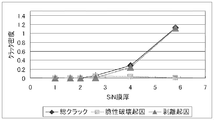
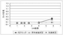
- the graph which shows the density of the crack resulting from the brittle fracture by stress, and its sum.
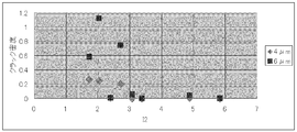
- the graph when a silicon nitride film is formed on a substrate having a different texture in the graph. Silicon nitride film whose texture is represented by I2 when a silicon nitride film is formed on the SiC substrate on which about 60 ⁇ m of CVD-SiC having various textures is formed by controlling the film forming conditions.
- the graph showing the crack density by the peeling origin.
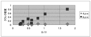
- the graph which expressed the texture for the crack density of the crack resulting from the brittle fracture by the internal stress of said formed silicon nitride film by I3 / I1.
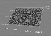
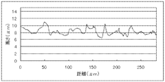
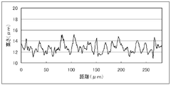
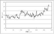
- FIG. 11 is an image photograph of the SiC-CVD texture with the fewest silicon nitride film cracks in FIG. 10. The above three-dimensional image photograph. The figure which shows said cross-sectional profile example.
- the SiC film formed on the semiconductor heat treatment member by the CVD method has various shapes and sizes of the SiC particles constituting the SiC film depending on the film forming conditions.
- FIG. 1 to FIG. 3 show surface properties of a surface portion of a typical CVD-SiC film observed with a laser microscope.
- the figure of (a) in each figure is an image figure by laser microscope observation, the figure of (b) shows the three-dimensional image figure by laser microscope observation, the figure of (c) shows a part of the figure of (a) horizontally. An example of the cross-sectional profile cut out in the direction is shown.
- FIG. 1 is a CVD-SiC film mainly composed of relatively large dome-shaped SiC particles
- FIG. 2 is a film mainly composed of relatively large pyramidal SiC particles
- FIG. 3 is a smooth structure composed of very fine SiC particles. 2 shows a laser micrograph image of a film-like film.
- the actual CVD-SiC coating is a complex combination of these, and the size of each particle varies, and there are coatings in which pyramidal particles are formed on dome-shaped particles.
- the ease of cracking and peeling of the deposit film cannot be uniformly determined by the surface roughness of the CVD-SiC film as in the prior art, but the surface properties of the CVD-SiC film ( Hereafter, it is known that it depends greatly on the texture).
- Table 1 shows a model in which a silicon nitride film having a thickness of 3 ⁇ m is formed on a textured CVD-SiC film entirely composed of single dome-shaped or pyramidal particles. Maximum stress is shown.
- the thickness is formed on a member on which a CVD-SiC film composed of a single dome-shaped or pyramidal single particle having a base L and a height H is formed on a SiC substrate. It is the result of simulating the stress acting on the interface between the SiC film and the silicon nitride film when a 3 ⁇ m thick silicon nitride film is formed by CVD.
- the maximum stress is caused by the difference in the representative length L of the particle and the shape, although the surface roughness Ra and Ry are both 4 ⁇ m. Is different.
- the maximum stress is large, the silicon nitride film is easily peeled off from the CVD-SiC film. Therefore, in the examples (a) to (c) in Table 1, the ease of peeling of the silicon nitride film changes.
- the likelihood of cracking changes depending on the typical length L of the particles and the difference in shape.
- the surface roughness Ra and Ry defining the conventional texture cannot represent the shape of the particles of these CVD-SiC coatings and the size of the individual particles.
- the texture of the SiC-CVD film could not be expressed accurately. Therefore, it was impossible to quantitatively grasp the ease of peeling or breaking the deposit film.
- the contact-type surface roughness meter has a problem that the surface irregularities due to very fine particles cannot be captured.
- SEM scanning electron microscope
- the inventors observed the CVD-SiC film with a laser microscope capable of obtaining three-dimensional quantitative dimension information, and obtained the CVD-SiC obtained by calculation from the observation result. It has been found that the texture can be expressed by I1 and I2, which are values obtained by integrating the Fourier amplitude spectrum of the cross-sectional profile of the film to which the cross-sectional profile of the film is applied with respect to ⁇ .
- the values of I1 and I2 vary depending on the number of peaks existing in the frequency ⁇ range and the height thereof, and the more peaks present in the frequency ⁇ range and the higher the height of each peak. Large value.
- the Fourier amplitude spectrum of the cross-sectional profile of the actual CVD-SiC film has a shape like a continuous spectrum because the peaks overlap, so the values of I1 and I2 are the values of each peak. Highly dependent on height.
- particles existing in the region of 0.01 ⁇ ⁇ ⁇ 0.02 are mainly dome-shaped particles, and particles existing in the region of 0.05 ⁇ ⁇ ⁇ 0.2 are mainly used. It was found to be a pyramidal or columnar particle.
- the texture is a mixture of dome-shaped particles and pyramidal or columnar particles. Further, in the region where I1 is smaller than 0.7 and I2 is smaller than 1.5, the growth of any of the dome-shaped pyramid-shaped particles is small, and the entire texture becomes smooth.
- FIGS. 1 to 3 the relationship between the numerical values of I1 and I2 and the texture will be specifically described.
- the inventors formed CVD-SiC films having various textures on the SiC substrate, and observed the texture of the surface portion with a laser microscope. Furthermore, a silicon nitride film used in the LPCVD process of actual semiconductor manufacturing was formed thereon by the LPCVD method, and the cracks generated in the CVD-SiC film and the state of peeling of the CVD-SiC film were observed. Through these observations, an attempt was made to clarify the relationship between cracks and delamination and the texture of the CVD-SiC film.
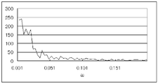
- the texture of the CVD-SiC film in the present invention was observed using a red laser microscope, a cross-sectional profile was calculated from the observed data, and the profile was converted into a Fourier amplitude spectrum with the observation length as the time axis.
- a red laser microscope As a method for converting to a Fourier amplitude spectrum, a red laser microscope has an observation length of 282 ⁇ m at a magnification of 500 times, a uniform pitch, and an observation length of a cross-sectional profile of a CVD-SiC film observed at 1024 measurement points. It was decided to convert to an amplitude spectrum.
- the integral value between the frequency ⁇ of the Fourier amplitude spectrum of 0.01 to 0.02 is I1
- the integral value of the frequency ⁇ from 0.05 to 0.2 is I2.
- An integrated value between the frequency ⁇ of 0.4 and 0.8 was set to I3.
- a CVD-SiC texture with an I1 of 0.9 or more, or a CVD-SiC film texture with an I1 of 0.9 or less and an I2 of 1.6 or more improves the adhesion of the deposit film, or deposits. It was found that there was an effect of remarkably suppressing the occurrence of cracks in the film. In order for these effects to be higher, it is preferable that I1 is 0.9 or less and I2 is 1.6 or more. More preferably, I1 is 0.4 or less and I2 is 1.6 or more. Particularly preferably, I2 is 3 or more and I3 / I1 is 0.6 or less.
- the values of I1, I2 and I3 change depending on the observation magnification of the laser microscope, and threshold values corresponding to each magnification may be set. However, noise is observed due to the influence of laser light reflection in the cross-sectional profile observed at a low magnification. Accurate profile may not be measured.
- the observation length becomes short, and it may not be possible to capture the entire texture by observing only specific particles.
- the diameter of a single particle can be several tens of ⁇ m, but if this is observed at a magnification of 1000 times or more, only one particle is observed. become.
- observation at 400 to 600 times is appropriate for the above reasons, and more preferably 500 times.
- the measurement of the cross-sectional profile for one observation image is performed five times or more, and these cross-sectional profiles and I1, I2 and I3 calculated therefrom are averaged to indicate the texture of the sample, I1 (average), I2 (Average) and I3 (Average).
- the cross-sectional profile is preferably measured 5 times or more at a pitch of 10 ⁇ m to 50 ⁇ m, and more preferably 5 times or more at a pitch of 20 to 30 ⁇ m.
- the present invention reduces the frequency of the cleaning process by depositing a thick deposit film in the LPCVD process in semiconductor manufacturing by controlling the CVD-SiC coating film of the CVD-SiC coated SiC heat treatment member to a texture in the above range. Became possible.
- the silicon nitride film is formed with a thickness of about 1.5 ⁇ m at a time.
- forced cooling is performed at a wind speed of about 1 m / second, and this film forming operation is repeated four times to form a silicon nitride film of about 6 ⁇ m in total. did.
- the number of cracks existing in the silicon nitride film was observed with an optical microscope.
- the texture of the CVD-SiC film on the SiC substrate was observed using a red laser microscope (manufactured by Keyence Corporation, model number VK8710).
- the observation length of the cross-sectional profile of the CVD-SiC film observed at 1024 ⁇ m and the number of measurement points of 1024 at an observation pitch of 282 ⁇ m at a magnification of 500 times was converted into a Fourier amplitude spectrum using the time axis as the observation length.
- the integral value between the frequency ⁇ of the Fourier amplitude spectrum of 0.01 to 0.02 is I1
- the integral value of the frequency ⁇ from 0.05 to 0.2 is I2.
- Eight cross-sectional profiles were measured so that the distance between the cross sections was 27.6 ⁇ m.
- I1 and I2 obtained from the cross-sectional profile are averaged, and I1 (average) and I2 (average) of the CVD-SiC film (hereinafter, I1 (average) and I2 (average) are simply referred to as I1 and I2).
- the number of cracks generated was significantly smaller than the number of cracks generated in the silicon nitride film coated on the other substrate.
- FIG. 5 is a graph in which the crack density in the silicon nitride film based on the above observation results is represented by a circle area, and the CVD-SiC film texture of each substrate is arranged in coordinates with the horizontal axis being I1 and the vertical axis being I2. is there.
- the area of the circle in this graph relatively represents the number per unit area of cracks generated in the silicon nitride film formed on the CVD-SiC film located in the coordinates. That is, if the area of the circle is large, it indicates that cracks in the numerical values of I1 and I2 are likely to occur. In the region where I1 is less than 0.9 and I2 is less than 1.6, a large number of large circles are scattered, and cracks are likely to occur in the nitride film formed on the substrate of the CVD-SiC film. Recognize.
- FIG. 6 shows the texture of the CVD-SiC film shown in FIG. 5 with the fewest cracks, ie, the smallest circle radius.
- a substrate on which a CVD-SiC film having a texture with I1 of 0.9 or more or I1 of 0.9 or less and I2 of 1.6 or more is formed on an SiC substrate by controlling the film forming conditions.
- a silicon nitride film was formed on each substrate by an LPCVD method with a thickness of about 6 ⁇ m. The silicon nitride film is formed to a thickness of about 1.5 ⁇ m at a time. After coating, forced cooling is performed at a wind speed of about 1 m / second, and this film forming operation is repeated four times to form a silicon nitride film up to a total of about 6 ⁇ m. Formed.
- the number of cracks present in the silicon nitride film was observed by classifying the silicon nitride film into a crack caused by peeling of the silicon nitride film and a crack caused by brittle fracture due to internal stress.
- the texture of the CVD-SiC film on the SiC substrate was observed using a red laser microscope (manufactured by Keyence Corporation, model number VK8710).
- the observation length of the cross-sectional profile of the CVD-SiC film observed at 1024 ⁇ m and the number of measurement points of 1024 at an observation pitch of 282 ⁇ m at a magnification of 500 times was converted into a Fourier amplitude spectrum using the time axis as the observation length.
- the integral value between the frequency ⁇ of the Fourier amplitude spectrum of 0.01 to 0.02 is I1
- the integral value of the frequency ⁇ is 0.05 to 0.2
- the frequency ⁇ is 0.4 ⁇ ⁇ ⁇ 0.
- the integral value up to 8 was defined as I3.
- Eight cross-sectional profiles were measured so that the distance between the cross sections was 27.6 ⁇ m.
- FIG. 7 (a) and 7 (b) show horizontal axes based on the above observation results when silicon nitride films are coated from about 1 ⁇ m to about 6 ⁇ m on samples having different values of I1, I2 and I3, respectively.
- 1 is an example of a graph showing the thickness of a silicon nitride film, the number of cracks per unit area of a crack caused by exfoliation of silicon nitride on the vertical axis, and a crack caused by brittle fracture caused by internal stress, and the sum thereof. It is shown that the number of cracks increases as the film thickness of the silicon nitride film increases, and the coating film is more easily broken as the film thickness of the silicon nitride film increases. On the other hand, in FIG.
- FIG. 8 is a graph showing the number of cracks per unit area due to peeling of the silicon nitride film on the horizontal axis and I2 on the horizontal axis for all samples coated with a silicon nitride film with thicknesses of about 4 ⁇ m and about 6 ⁇ m. It is. As I2 increases, the number of cracks decreases. In particular, in the region where I2 exceeds 3, there are almost no cracks due to peeling, and it can be seen that peeling hardly occurs.
- FIG. 9 shows the I3 / I1 on the horizontal axis and the number of cracks per unit area due to brittle fracture of the silicon nitride film on the vertical axis for all samples coated with a silicon nitride film with a thickness of about 4 ⁇ m and about 6 ⁇ m. It is a represented graph. When the silicon nitride film exceeds 4 ⁇ m, cracks are prominent. However, the smaller I3 / I1 is, the smaller the cracks are. It turns out that it is hard to generate.
- FIG. 10 shows the crack density in the silicon nitride film according to the above observation results as a circle area, and the CVD-SiC film texture of each substrate is arranged in the coordinates where the horizontal axis is I2 and the vertical axis is I3 / I1. It is a graph.
- the area of the circle in this graph is the sum of the cracks caused by the silicon nitride film peeling generated in the silicon nitride film formed on the CVD-SiC film located in the coordinates and the cracks caused by brittle fracture.
- the number per unit area is relatively represented. That is, if the area of the circle is large, it indicates that cracks in the numerical values of I2 and I3 / I1 are likely to occur.
- FIG. 11 shows the texture of the CVD-SiC film having the fewest cracks in FIG. 10, that is, the smallest circle radius.
- the present invention can be used for a semiconductor heat treatment member having a SiC film in an LPCVD process in a semiconductor manufacturing process. It should be noted that the entire contents of the specification, claims, drawings and abstract of Japanese Patent Application No. 2009-107932 filed on April 27, 2009 are cited here as disclosure of the specification of the present invention. Incorporated.
Landscapes
- Chemical & Material Sciences (AREA)
- General Chemical & Material Sciences (AREA)
- Chemical Kinetics & Catalysis (AREA)
- Engineering & Computer Science (AREA)
- Materials Engineering (AREA)
- Mechanical Engineering (AREA)
- Metallurgy (AREA)
- Organic Chemistry (AREA)
- Inorganic Chemistry (AREA)
- Chemical Vapour Deposition (AREA)
Abstract
Description
本発明は、クリーニング工程の頻度を低下させ、ウェハー処理のスループットを著しく向上できるCVD-SiC被膜を有する半導体熱処理部材、及び半導体熱処理部材用をSiC被膜の評価方法を提供することを目的とする。
1.CVD-SiC被膜を備える半導体熱処理部材であって、前記CVD-SiC被膜について、下記(1)~(6)の手順に従って求めたI1(平均)とI2(平均)の数値が下記の(A)又は(B)を満足することを特徴とする半導体熱処理部材。
(A)I1(平均)が0.9以下であり、かつI2(平均)が1.6以上である。
(B)I1(平均)が0.9以上である
(1)CVD-SiC被膜について、レーザ顕微鏡で、倍率400~600で、CVD-SiC被膜の表面観察を行う。
(2)レーザ顕微鏡で観察したCVD-SiC被膜から、断面間の間隔が10μm以上50μm以下のピッチで5箇所以上、断面プロファイルを測定する。
(3)断面プロファイルの測定値をフーリエ変換する。
(4)フーリエ変換データからフーリエ振幅スペクトルを計算する。
(5)フーリエ振幅スペクトルを、I1の積分範囲を0.01≦ω≦0.02、I2の積分範囲を0.05≦ω≦0.2とし、周波数(ω)で定積分し、I1とI2とを求める。
(6)X方向に5箇所以上測定した断面プロファイルから求めたI1とI2とをそれぞれ平均して、CVD-SiC被膜のI1(平均)とI2(平均)とする。
2.前記I1(平均)が0.4以下であり、かつ前記I2(平均)が1.6以上である上記1に記載の半導体熱処理部材。
3.前記I2(平均)が3以上で、かつ、前記フーリエ振幅スペクトルの積分範囲を0.4≦ω≦0.8として定積分して求めたI3を断面間の間隔が10μm以上50μm以下のピッチで5箇所以上測定した断面プロファイルから求めたI3を平均してもとめたI3(平均)と前記I1(平均)の比(I3(平均)/I1(平均))が0.6以下である上記1に記載の半導体熱処理部材。
4.CVD-SiC被膜を備える半導体熱処理部材におけるSiC被膜の評価方法であって、下記(1)~(6)の手順に従って求めたI1(平均)とI2(平均)を用いて、前記CVD-SiC被膜の表面性状を表すことを特徴とする半導体熱処理部材用SiC被膜の評価方法。
(1)CVD-SiC被膜について、レーザ顕微鏡で、倍率400~600で、CVD-SiC被膜の表面観察を行う。
(2)レーザ顕微鏡で観察したCVD-SiC被膜から、断面間の間隔が10μm以上50μm以下のピッチで5箇所以上断面プロファイルを測定する。
(3)断面プロファイルの測定値をフーリエ変換する。
(4)フーリエ変換データからフーリエ振幅スペクトルを計算する。
(5)フーリエ振幅スペクトルを、I1の積分範囲を0.01≦ω≦0.02、I2の積分範囲を0.05≦ω≦0.2とし、周波数(ω)で定積分し、I1とI2とを求める。
(6)10μm以上50μm以下のピッチで5箇所以上測定した断面プロファイルから求めたI1とI2とをそれぞれ平均して、CVD-SiC被膜のI1(平均)とI2(平均)とする。
5.CVD-SiC被膜を備える半導体熱処理部材におけるSiC被膜の評価方法であって、下記(1)~(8)の手順に従って求めたI1(平均)、I2(平均)及びI3(平均)を用いて、前記CVD-SiC被膜の表面性状を表すことを特徴とする半導体熱処理部材用SiC被膜の評価方法。
(1)CVD-SiC被膜について、レーザ顕微鏡で、倍率400~600で、CVD-SiC被膜の表面観察を行う。
(2)レーザ顕微鏡で観察したCVD-SiC被膜から、断面間の間隔が5μm以上10μm以下のピッチで5箇所以上、断面プロファイルを測定する。
(3)断面プロファイルの測定値をフーリエ変換する。
(4)フーリエ変換データからフーリエ振幅スペクトルを計算する。
(5)フーリエ振幅スペクトルを、I1の積分範囲を0.01≦ω≦0.02、I2の積分範囲を0.05≦ω≦0.2とし、周波数(ω)で定積分し、I1とI2とを求める。
(6)10μm以上50μm以下のピッチで5箇所以上測定した断面プロファイルから求めたI1とI2とをそれぞれ平均して、CVD-SiC被膜のI1(平均)とI2(平均)とする。
(7)フーリエ振幅スペクトルを、I3の積分範囲を0.4≦ω≦0.8とし、周波数(ω)で定積分し、I3を求める。
(8)X方向に5箇所以上測定した断面プロファイルから求めたI3を平均して、CVD-SiC被膜のI3(平均)とする。

また、I1が0.7より小さくかつI2が1.5より小さい領域では、ドーム状ピラミッド状のいずれの粒子とも成長が小さく、全体としてはスムースなテクスチャーとなる。
SiC基板の上のCVD-SiC被膜のテクスチャーは、赤色レーザ顕微鏡(キーエンス社製、型番VK8710)を用いて観測した。500倍の倍率で観測長を282μm、均等ピッチで、測定点数1024点で観測したCVD-SiC被膜の断面プロファイルの観測長を時間軸としてフーリエ振幅スペクトルに変換した。フーリエ振幅スペクトルの周波数ωが0.01~0.02の間の積分値をI1、周波数ωが0.05~0.2までの積分値をI2とした。断面間の間隔が27.6μmになるようにして、8箇所断面プロファイルを測定した。断面プロファイルから求めたI1とI2とをそれぞれ平均して、CVD-SiC被膜のI1(平均)とI2(平均)(なお、以下において、I1(平均)およびI2(平均)をそれぞれ、単にI1およびI2という。)とした。
SiC基板の上のCVD-SiC被膜のテクスチャーは、赤色レーザ顕微鏡(キーエンス社製、型番VK8710)を用いて観測した。500倍の倍率で観測長を282μm、均等ピッチで、測定点数1024点で観測したCVD-SiC被膜の断面プロファイルの観測長を時間軸としてフーリエ振幅スペクトルに変換した。フーリエ振幅スペクトルの周波数ωが0.01~0.02の間の積分値をI1、周波数ωが0.05~0.2までの積分値をI2、周波数ωが0.4≦ω≦0.8までの積分値をI3とした。断面間の間隔が27.6μmになるようにして、8箇所断面プロファイルを測定した。断面プロファイルから求めたI1、I2及びI3とをそれぞれ平均して、CVD-SiC被膜のI1(平均)、I2(平均)及びI3(平均)(なお、以下において、I1(平均)、I2(平均)およびI3(平均)をそれぞれ、単に、I1、I2およびI3という。)とした。
図7(a)および図7(b)は、それぞれI1、I2およびI3の値が異なるサンプル上に窒化ケイ素膜を約1μmから約6μmまでコーティングしたときに、上記観測結果に基いて横軸に窒化ケイ素膜厚み、縦軸に窒化ケイ素の剥離起因によるクラックと内部応力による脆性破壊起因によるクラックの単位面積当たりのクラック数とその総和を表したグラフの一例である。窒化ケイ素膜の膜厚が大きくなるほどクラックの数が増え、窒化ケイ素膜の膜厚が厚くなるほどコーティング膜が破壊され易いことが表されている。
一方、図7(a)では窒化ケイ素膜のクラックの大部分が窒化ケイ素膜の剥離に起因するクラックであるのに対して、図7(b)はクラックの数は少ないが、クラックの大部分は内部応力による脆性破壊起因によるクラックであった。このように、テクスチャーの違いによって窒化ケイ素膜の破壊メカニズムが異なることが表されており、特に窒化ケイ素膜に剥離が発生すると膜の破壊が急速に進展することが分かる。
図8は、約4μmと約6μmの厚味で窒化ケイ素膜をコーティングした全てのサンプルについて、横軸にI2、縦軸に窒化ケイ素膜の剥離起因によるクラックの単位面積当たりの数を表したグラフである。I2が大きくなるほどクラックは少なくなり、特にI2が3を超える領域において剥離起因におけるクラックは殆ど存在せず、剥離がほぼ発生していないことが分かる。
図9は、約4μmと約6μmの厚味で窒化ケイ素膜をコーティングした全てのサンプルについて、横軸にI3/I1、縦軸に窒化ケイ素膜の脆性破壊起因によるクラックの単位面積当たりの数を表したグラフである。窒化ケイ素膜が4μmを超えるとクラックの発生が顕著であるが、I3/I1が小さくなるほどクラックは少なくなり、特にI3/I1が0.6より小さい領域においてクラックが少なく脆性破壊起因によるクラックがほぼ発生し難いことが分かる。
図10は、上記観測結果による窒化ケイ素膜中のクラック密度を円の面積で表し、各基板のCVD-SiC被膜テクスチャーを、横軸をI2、縦軸をI3/I1とした座標中に配置したグラフである。このグラフ中の円の面積は、上記座標中に位置するCVD-SiC被膜上に製膜された窒化ケイ素膜中に発生した窒化ケイ素膜剥離に起因するクラックと脆性破壊に起因するクラックの和を単位面積当りの数を相対的に表している。即ち、円の面積が大きければ、そのI2とI3/I1の数値におけるクラックが発生しやすいことを示している。I2が3以上でかつI3/I1が0.4以下の領域では円の面積が他の領域よりも小さく、CVD-SiC被膜の基板に製膜された窒化膜中にクラックが発生し難いことがわかる。図11に図10中最もクラックが少ない、即ち最も円の半径が小さかったCVD-SiC皮膜のテクスチャーを示す。図10のI2とI3/I1の値はそれぞれI2=5.452、I3/I1=0.322であった。
なお、2009年4月27日に出願された日本特許出願2009-107932号の明細書、特許請求の範囲、図面及び要約書の全内容をここに引用し、本発明の明細書の開示として、取り入れるものである。
Claims (5)
- CVD-SiC被膜を備える半導体熱処理部材であって、前記CVD-SiC被膜について、下記(1)~(6)の手順に従って求めたI1(平均)とI2(平均)の数値が下記の(A)又は(B)を満足することを特徴とする半導体熱処理部材。
(A)I1(平均)が0.9以下であり、かつI2(平均)が1.6以上である。
(B)I1(平均)が0.9以上である。
(1)CVD-SiC被膜について、レーザ顕微鏡で、倍率400~600で、CVD-SiC被膜の表面観察を行う。
(2)レーザ顕微鏡で観察したCVD-SiC被膜から、断面間の間隔が10μm以上50μm以下のピッチで5箇所以上断面プロファイルを測定する。
(3)断面プロファイルの測定値をフーリエ変換する。
(4)フーリエ変換データからフーリエ振幅スペクトルを計算する。
(5)フーリエ振幅スペクトルを、I1の積分範囲を0.01≦ω≦0.02、I2の積分範囲を0.05≦ω≦0.2とし、周波数(ω)で定積分し、I1とI2とを求める。
(6)X方向に5箇所以上測定した断面プロファイルから求めたI1とI2とをそれぞれ平均して、CVD-SiC被膜のI1(平均)とI2(平均)とする。 - 前記I1(平均)が0.4以下であり、かつ前記I2(平均)が1.6以上である請求項1に記載の半導体熱処理部材。
- 前記I2(平均)が3以上で、かつ、前記フーリエ振幅スペクトルの積分範囲を0.4≦ω≦0.8として定積分して求めたI3について、断面間の間隔が10μm以上50μm以下のピッチで5箇所以上測定した断面プロファイルから求めたI3を平均してもとめたI3(平均)と前記I1(平均)の比(I3(平均)/I1(平均))が0.6以下である請求項1に記載の半導体熱処理部材。
- CVD-SiC被膜を備える半導体熱処理部材におけるSiC被膜の評価方法であって、下記(1)~(6)の手順に従って求めたI1(平均)とI2(平均)を用いて、前記CVD-SiC被膜の表面性状を表すことを特徴とする半導体熱処理部材用SiC被膜の評価方法。
(1)CVD-SiC被膜について、レーザ顕微鏡で、倍率400~600で、CVD-SiC被膜の表面観察を行う。
(2)レーザ顕微鏡で観察したCVD-SiC被膜から、断面間の間隔が10μm以上50μm以下のピッチで、5箇所以上断面プロファイルを測定する。
(3)断面プロファイルの測定値をフーリエ変換する。
(4)フーリエ変換データからフーリエ振幅スペクトルを計算する。
(5)フーリエ振幅スペクトルを、I1の積分範囲を0.01≦ω≦0.02、I2の積分範囲を0.05≦ω≦0.2とし、周波数(ω)で定積分し、I1とI2とを求める。
(6)X方向に5箇所以上測定した断面プロファイルから求めたI1とI2とをそれぞれ平均して、CVD-SiC被膜のI1(平均)とI2(平均)とする。 - CVD-SiC被膜を備える半導体熱処理部材におけるSiC被膜の評価方法であって、下記(1)~(8)の手順に従って求めたI1(平均)、I2(平均)及びI3(平均)を用いて、前記CVD-SiC被膜の表面性状を表すことを特徴とする半導体熱処理部材用SiC被膜の評価方法。
(1)CVD-SiC被膜について、レーザ顕微鏡で、倍率400~600で、CVD-SiC被膜の表面観察を行う。
(2)レーザ顕微鏡で観察したCVD-SiC被膜から、断面間の間隔が10μm以上50μm以下のピッチで、5箇所以上断面プロファイルを測定する。
(3)断面プロファイルの測定値をフーリエ変換する。
(4)フーリエ変換データからフーリエ振幅スペクトルを計算する。
(5)フーリエ振幅スペクトルを、I1の積分範囲を0.01≦ω≦0.02、I2の積分範囲を0.05≦ω≦0.2とし、周波数(ω)で定積分し、I1とI2とを求める。
(6)X方向に5箇所以上測定した断面プロファイルから求めたI1とI2とをそれぞれ平均して、CVD-SiC被膜のI1(平均)とI2(平均)とする。
(7)フーリエ振幅スペクトルを、I3の積分範囲を0.4≦ω≦0.8とし、周波数(ω)で定積分し、I3を求める。
(8)X方向に5箇所以上測定した断面プロファイルから求めたI3を平均して、CVD-SiC被膜のI3(平均)とする。
Priority Applications (3)
| Application Number | Priority Date | Filing Date | Title |
|---|---|---|---|
| JP2011511364A JP5585577B2 (ja) | 2009-04-27 | 2010-04-14 | 半導体熱処理部材用SiC被膜の評価方法 |
| SG2011071917A SG175038A1 (en) | 2009-04-27 | 2010-04-14 | Semiconductor heat treatment member comprising sic film |
| US13/281,680 US20120041714A1 (en) | 2009-04-27 | 2011-10-26 | Semiconductor heat treatment member having sic film |
Applications Claiming Priority (2)
| Application Number | Priority Date | Filing Date | Title |
|---|---|---|---|
| JP2009107932 | 2009-04-27 | ||
| JP2009-107932 | 2009-04-27 |
Related Child Applications (1)
| Application Number | Title | Priority Date | Filing Date |
|---|---|---|---|
| US13/281,680 Continuation US20120041714A1 (en) | 2009-04-27 | 2011-10-26 | Semiconductor heat treatment member having sic film |
Publications (1)
| Publication Number | Publication Date |
|---|---|
| WO2010125918A1 true WO2010125918A1 (ja) | 2010-11-04 |
Family
ID=43032071
Family Applications (1)
| Application Number | Title | Priority Date | Filing Date |
|---|---|---|---|
| PCT/JP2010/056712 Ceased WO2010125918A1 (ja) | 2009-04-27 | 2010-04-14 | SiC被膜を有する半導体熱処理部材 |
Country Status (6)
| Country | Link |
|---|---|
| US (1) | US20120041714A1 (ja) |
| JP (1) | JP5585577B2 (ja) |
| KR (1) | KR20120006492A (ja) |
| SG (2) | SG2014015127A (ja) |
| TW (1) | TW201101405A (ja) |
| WO (1) | WO2010125918A1 (ja) |
Citations (3)
| Publication number | Priority date | Publication date | Assignee | Title |
|---|---|---|---|---|
| JPH0415913A (ja) * | 1990-05-10 | 1992-01-21 | Furukawa Electric Co Ltd:The | 有機金属気相成長法とそれに用いるサセプタ |
| JP2005311290A (ja) * | 2004-03-23 | 2005-11-04 | Toshiba Ceramics Co Ltd | サセプタ |
| JP2006237498A (ja) * | 2005-02-28 | 2006-09-07 | Rohm Co Ltd | サセプタ |
Family Cites Families (3)
| Publication number | Priority date | Publication date | Assignee | Title |
|---|---|---|---|---|
| US6782337B2 (en) * | 2000-09-20 | 2004-08-24 | Kla-Tencor Technologies Corp. | Methods and systems for determining a critical dimension an a presence of defects on a specimen |
| JP2006038779A (ja) * | 2004-07-30 | 2006-02-09 | Hitachi High-Technologies Corp | パターン形状評価方法、評価装置、及び半導体装置の製造方法 |
| US20100235114A1 (en) * | 2009-03-10 | 2010-09-16 | Kla-Tencor Corporation | Systems and methods for determining one or more characteristics of a specimen using radiation in the terahertz range |
-
2010
- 2010-04-14 JP JP2011511364A patent/JP5585577B2/ja active Active
- 2010-04-14 SG SG2014015127A patent/SG2014015127A/en unknown
- 2010-04-14 WO PCT/JP2010/056712 patent/WO2010125918A1/ja not_active Ceased
- 2010-04-14 KR KR1020117022611A patent/KR20120006492A/ko not_active Withdrawn
- 2010-04-14 SG SG2011071917A patent/SG175038A1/en unknown
- 2010-04-23 TW TW099112855A patent/TW201101405A/zh unknown
-
2011
- 2011-10-26 US US13/281,680 patent/US20120041714A1/en not_active Abandoned
Patent Citations (3)
| Publication number | Priority date | Publication date | Assignee | Title |
|---|---|---|---|---|
| JPH0415913A (ja) * | 1990-05-10 | 1992-01-21 | Furukawa Electric Co Ltd:The | 有機金属気相成長法とそれに用いるサセプタ |
| JP2005311290A (ja) * | 2004-03-23 | 2005-11-04 | Toshiba Ceramics Co Ltd | サセプタ |
| JP2006237498A (ja) * | 2005-02-28 | 2006-09-07 | Rohm Co Ltd | サセプタ |
Also Published As
| Publication number | Publication date |
|---|---|
| JPWO2010125918A1 (ja) | 2012-10-25 |
| SG175038A1 (en) | 2011-11-28 |
| JP5585577B2 (ja) | 2014-09-10 |
| SG2014015127A (en) | 2014-06-27 |
| US20120041714A1 (en) | 2012-02-16 |
| TW201101405A (en) | 2011-01-01 |
| KR20120006492A (ko) | 2012-01-18 |
Similar Documents
| Publication | Publication Date | Title |
|---|---|---|
| US20230227375A1 (en) | Plasma-resistant member | |
| RU2195045C2 (ru) | Деталь из кварцевого стекла для применения при изготовлении полупроводников | |
| JP2018511943A (ja) | フッ化アニールした膜でコーティングした物品 | |
| JP2017534001A (ja) | プラズマ耐エッチング性が向上された工程部品及びそのプラズマ耐エッチング性の強化処理方法 | |
| CN110246811A (zh) | 复合结构物和其评价方法、半导体和显示屏制造装置 | |
| TWI862956B (zh) | 零部件、等離子體裝置、形成耐腐蝕塗層的方法及其裝置 | |
| JP6597922B1 (ja) | 複合構造物および複合構造物を備えた半導体製造装置並びにディスプレイ製造装置 | |
| EP2559791A1 (en) | Single-crystal substrate, single-crystal substrate having crystalline film, crystalline film, method for producing single-crystal substrate having crystalline film, method for producing crystalline substrate, and method for producing element | |
| TW201545198A (zh) | 電感耦合型等離子體處理腔室及其抗腐蝕絕緣視窗及製造方法 | |
| JP5652402B2 (ja) | 半導体製造用治具及びその製造方法 | |
| JP5585577B2 (ja) | 半導体熱処理部材用SiC被膜の評価方法 | |
| CN107833842B (zh) | 一种3d nand存储器的层叠结构的薄膜层厚度测量方法 | |
| TWI249510B (en) | Silica glass jig used in process for manufacturing semiconductor and method of manufacturing silica glass jig | |
| JP6358492B2 (ja) | 耐プラズマ性部材 | |
| CN114755074B (zh) | 物性分析方法、物性分析试片及其制备方法 | |
| KR20190032719A (ko) | 반도체 웨이퍼용 고효율 히터블럭 및 그 제조방법 | |
| Chang et al. | Nearly Zero Reflectance of Nano-Pyramids and Dual-Antireflection Coating Structure for Monocrystalline Silicon Solar Cells | |
| CN115579302A (zh) | 一种用于非标厚度硅片的量测方法及切片机 | |
| Velichko et al. | Influence of the surface microroughness of a Si (001) substrate on the morphology of CaF2 epitaxial layers under high-temperature growth conditions | |
| Kim et al. | Surface Texturing of Si with Periodically Arrayed Oblique Nanopillars to Achieve Antireflection. Materials 2021, 14, 380 | |
| KR20240177971A (ko) | 반도체 챔버용 pvd 코팅층 및 이의 제조방법 | |
| JPWO2020183914A1 (ja) | 表面微細構造および表面微細構造を備えた基体 | |
| CN120033050A (zh) | 半导体零部件及其涂层形成方法 |
Legal Events
| Date | Code | Title | Description |
|---|---|---|---|
| 121 | Ep: the epo has been informed by wipo that ep was designated in this application |
Ref document number: 10769617 Country of ref document: EP Kind code of ref document: A1 |
|
| WWE | Wipo information: entry into national phase |
Ref document number: 2011511364 Country of ref document: JP |
|
| ENP | Entry into the national phase |
Ref document number: 20117022611 Country of ref document: KR Kind code of ref document: A |
|
| NENP | Non-entry into the national phase |
Ref country code: DE |
|
| 122 | Ep: pct application non-entry in european phase |
Ref document number: 10769617 Country of ref document: EP Kind code of ref document: A1 |