WO2010122845A1 - 光学補償フィルムの製造方法 - Google Patents
光学補償フィルムの製造方法 Download PDFInfo
- Publication number
- WO2010122845A1 WO2010122845A1 PCT/JP2010/053636 JP2010053636W WO2010122845A1 WO 2010122845 A1 WO2010122845 A1 WO 2010122845A1 JP 2010053636 W JP2010053636 W JP 2010053636W WO 2010122845 A1 WO2010122845 A1 WO 2010122845A1
- Authority
- WO
- WIPO (PCT)
- Prior art keywords
- temperature
- coating
- liquid crystal
- film
- optical compensation
- Prior art date
- Legal status (The legal status is an assumption and is not a legal conclusion. Google has not performed a legal analysis and makes no representation as to the accuracy of the status listed.)
- Ceased
Links
Images

Classifications
-
- G—PHYSICS
- G02—OPTICS
- G02B—OPTICAL ELEMENTS, SYSTEMS OR APPARATUS
- G02B5/00—Optical elements other than lenses
- G02B5/30—Polarising elements
- G02B5/3025—Polarisers, i.e. arrangements capable of producing a definite output polarisation state from an unpolarised input state
- G02B5/3033—Polarisers, i.e. arrangements capable of producing a definite output polarisation state from an unpolarised input state in the form of a thin sheet or foil, e.g. Polaroid
- G02B5/3041—Polarisers, i.e. arrangements capable of producing a definite output polarisation state from an unpolarised input state in the form of a thin sheet or foil, e.g. Polaroid comprising multiple thin layers, e.g. multilayer stacks
- G02B5/305—Polarisers, i.e. arrangements capable of producing a definite output polarisation state from an unpolarised input state in the form of a thin sheet or foil, e.g. Polaroid comprising multiple thin layers, e.g. multilayer stacks including organic materials, e.g. polymeric layers
-
- G—PHYSICS
- G02—OPTICS
- G02B—OPTICAL ELEMENTS, SYSTEMS OR APPARATUS
- G02B5/00—Optical elements other than lenses
- G02B5/30—Polarising elements
- G02B5/3083—Birefringent or phase retarding elements
-
- G—PHYSICS
- G02—OPTICS
- G02F—OPTICAL DEVICES OR ARRANGEMENTS FOR THE CONTROL OF LIGHT BY MODIFICATION OF THE OPTICAL PROPERTIES OF THE MEDIA OF THE ELEMENTS INVOLVED THEREIN; NON-LINEAR OPTICS; FREQUENCY-CHANGING OF LIGHT; OPTICAL LOGIC ELEMENTS; OPTICAL ANALOGUE/DIGITAL CONVERTERS
- G02F1/00—Devices or arrangements for the control of the intensity, colour, phase, polarisation or direction of light arriving from an independent light source, e.g. switching, gating or modulating; Non-linear optics
- G02F1/01—Devices or arrangements for the control of the intensity, colour, phase, polarisation or direction of light arriving from an independent light source, e.g. switching, gating or modulating; Non-linear optics for the control of the intensity, phase, polarisation or colour
- G02F1/13—Devices or arrangements for the control of the intensity, colour, phase, polarisation or direction of light arriving from an independent light source, e.g. switching, gating or modulating; Non-linear optics for the control of the intensity, phase, polarisation or colour based on liquid crystals, e.g. single liquid crystal display cells
- G02F1/133—Constructional arrangements; Operation of liquid crystal cells; Circuit arrangements
- G02F1/1333—Constructional arrangements; Manufacturing methods
- G02F1/1335—Structural association of cells with optical devices, e.g. polarisers or reflectors
- G02F1/13363—Birefringent elements, e.g. for optical compensation
- G02F1/133633—Birefringent elements, e.g. for optical compensation using mesogenic materials
Definitions
- the present invention relates to a method for producing an optical compensation film. More specifically, the present invention relates to an optical compensation film having a retardation layer in which rod-like polymerizable liquid crystal compounds (hereinafter also simply referred to as polymerizable liquid crystal compounds) are vertically aligned and fixed. It relates to a manufacturing method.
- rod-like polymerizable liquid crystal compounds hereinafter also simply referred to as polymerizable liquid crystal compounds
- the transverse electric field switching mode type liquid crystal display device is excellent in contrast, viewing angle and the like for the liquid crystal mode of other liquid crystal display devices, for example, TN mode, and for the vertical alignment mode (VA, MVA, PVA, etc.). It has excellent display performance such as viewing angle, and has excellent effects such as a small change in luminance due to viewing angle and a small drop in response speed in halftones, so it is marketed as a so-called IPS (In Plane Switching) type liquid crystal display device. It came to be provided actively.
- Examples of the IPS mode type liquid crystal display device include an FFS (fringe field switching) mode and an FLC (ferroelectric liquid crystal) mode in addition to the so-called IPS mode.
- FFS field switching
- FLC ferrroelectric liquid crystal
- JP 2005-309379 A discloses a polarizing plate using an optical compensation film provided with a retardation layer having a vertically aligned rod-like liquid crystal compound
- JP 2005-265889 A describes retardation.
- the liquid crystal compound After coating a coating liquid containing a polymerizable liquid crystal compound on a support, forming a liquid crystal compound layer, and drying the liquid crystal compound layer, the liquid crystal compound is heated and aligned at a temperature equal to or higher than the liquid crystal transition temperature, and ultraviolet rays are irradiated.
- a method of heating the optically anisotropic layer after irradiation and fixing the orientation is known (for example, see Patent Document 2).
- Patent Document 1 and Patent Document 2 are effective methods for aligning rod-shaped polymerizable liquid crystal compounds, but are insufficient for surface roughness, alignment defects, and haze increase. It turned out that.
- the present invention has been made in view of the above circumstances, and an object thereof is to provide a method for producing an optical compensation film having a retardation layer having a polymerizable liquid crystal compound and having less surface roughness, alignment defects, and haze increase. That is.
- the method for producing an optical compensation film having an orientation step after the drying step and a curing step of irradiating the coating film with active radiation,
- the method for producing an optical compensation film wherein the coating solution is heated from + 5 ° C. to + 40 ° C. than the temperature at the time of coating, and then the temperature is lowered to the coating temperature and coated on the support.
- FIG. 1 is a schematic view showing a configuration of a liquid crystal display device using an optical compensation film.
- FIG. 1A is a schematic diagram showing a configuration of a liquid crystal display device using an optical compensation film having a retardation layer on the viewing side polarizing plate.
- FIG. 1B is a schematic view showing a configuration of a liquid crystal display device using an optical compensation film having a retardation layer on a backlight side polarizing plate.
- the liquid crystal display device 1 a includes a liquid crystal cell 101 sandwiched between a viewing side polarizing plate 102 and a backlight side polarizing plate 103.
- the liquid crystal cell 101 includes a liquid crystal layer 101c sandwiched between a glass substrate 101a and a glass substrate 101b.
- the viewing-side polarizing plate 102 has a first protective film 102a and a second protective film having a retardation layer 102c in which the orientation of the polymerizable liquid crystal compound is fixed on the liquid crystal cell 101 side from the viewing side (shown in the upper part of the figure).
- the first polarizing film 102d is sandwiched between the first polarizing film 102b and the second polarizing film 102d.
- the second protective film 102b having the retardation layer 102c is referred to as an optical compensation film.
- the backlight side polarizing plate 103 includes a second polarizing film 103c sandwiched between a third protective film 103a and a fourth protective film 103b.
- the retardation layer 102c may be disposed between the first polarizing film 102d and the second protective film 102b.
- the in-plane slow axis b (the arrow direction in the figure) of the second protective film 102b and the alignment direction c (the arrow direction in the figure) of the liquid crystal layer 101c are parallel.
- the polarization transmission axis a (the arrow direction in the figure) of the polarizing film and the rubbing axis d (the arrow direction in the figure) of the glass substrate are in the direction shown in the figure.
- the liquid crystal display device shown in FIG. In the figure, 1b denotes a liquid crystal display device.
- the liquid crystal display device 1b includes a viewing-side polarizing plate 102 'and a liquid crystal cell 101' sandwiched between the backlight-side polarizing plate 103 '.
- the liquid crystal cell 101 ′ has a configuration including a liquid crystal layer 101′c sandwiched between a glass substrate 101′a and a glass substrate 101′b.
- the viewing-side polarizing plate 102 includes a second polarizing film 102'c sandwiched between a fourth protective film 102'a and a third protective film 102'b from the viewing side (showing the upper side in the figure). It has composition which has.
- the backlight-side polarizing plate 103 ' is formed on a second protective film 103'a and a first protective film 103'b having a retardation layer 103'c in which the orientation of the rod-like liquid crystal compound is fixed on the liquid crystal cell 101' side.
- the first polarizing film 103′d is sandwiched.
- the second protective film 103′a having the retardation layer 103′c is referred to as an optical compensation film.
- the retardation layer 103′c may be disposed between the first polarizing film 103′d and the second protective film 103′a.
- the in-plane slow axis b (the arrow direction in the figure) of the second protective film 103'a and the alignment direction c (the arrow direction in the figure) of the liquid crystal layer 101'c are orthogonal to each other.
- the polarization transmission axis a (the arrow direction in the figure) of the polarizing film and the rubbing axis d (the arrow direction in the figure) of the glass substrate are in the direction shown in the figure.
- the present invention relates to a method for producing the optical compensation film shown in the figure.
- the optical compensation film according to the method for producing an optical compensation film of the present invention is obtained by applying a solution of a polymerizable liquid crystal compound on a resin film base material, and subjecting the polymerizable liquid crystal compound to orientation through drying, heat application processing and an orientation step. It is characterized by having a retardation layer made of a vertically aligned polymerizable liquid crystal compound that is fixed by actinic radiation curing or thermal polymerization. Note that the vertical alignment is a black color when the retardation layer is sandwiched between crossed Nicol polarizing films when evaluated using a polarizing microscope in order to evaluate the optical retardation of the obtained retardation layer.
- the one that appears white is defined as being vertically aligned.
- a so-called vertical alignment film may be used, and the vertical alignment film is not particularly limited.
- the alignment film is not particularly necessary when it extends to the interface opposite to that, and it is preferable from the viewpoint of simplifying the configuration.
- the retardation layer of the optical compensation film according to the method for producing an optical compensation film of the present invention is formed by a vertically aligned polymerizable liquid crystal compound having a retardation Ro in the range of 0 nm to 10 nm and a retardation Rt in the range of ⁇ 100 nm to ⁇ 400 nm.
- a phase difference layer is preferred.
- Ro is more preferably in the range of 0 nm to 5 nm.
- the thickness of the retardation layer, actinic radiation irradiation, the temperature during curing, the tilt angle control, and the pretilt angle at the support / air interface can be controlled. preferable.
- Ro shows in-plane retardation
- Rt shows thickness direction retardation
- Formula (i) Ro (nx ⁇ ny) ⁇ d
- Formula (ii) Rt ((nx + ny) / 2 ⁇ nz) ⁇ d (Where nx is the refractive index in the slow axis direction in the retardation layer surface, ny is the refractive index in the fast axis direction in the retardation layer surface, nz is the refractive index in the thickness direction of the retardation layer (refractive index is 23 Measured at a wavelength of 590 nm under an environment of ° C. and 55% RH), d represents the thickness (nm) of the retardation layer.
- an automatic birefringence meter KOBURA 21ADH manufactured by Oji Scientific Instruments was used, and the measurement was performed at 23 ° C. and 55% RH at a wavelength of 590 nm.
- Optical compensation film has very strict performance requirements, and even a few coating failures (defects) can have a great effect on optical properties.
- the present invention relates to a method for producing an optical compensation film with less surface roughness, alignment defects, and haze increase by subjecting a coating liquid for forming a polymerizable liquid crystal compound layer before coating to a temperature rise. Next, the method for producing the optical compensation film of the present invention will be described.
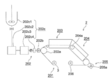
- FIG. 2 is a schematic diagram of the optical compensation film manufacturing process.
- the manufacturing process 2 includes a resin film supply process 201 as a support, a coating process 202, a drying process 203, an orientation process 204, a curing process 205, and a recovery process 206 in order.
- the resin film supply step 201 uses a feeding device (not shown) for the resin film 3 wound in a roll shape, and supplies the resin film 3 to the coating step 202.
- the coating step 202 uses a back roll 202a that holds the resin film 3, a coating device 202b, and a coating liquid preparation device 202c.
- the coating liquid preparation apparatus 202c has a coating liquid preparation tank 202c1, a coating liquid temperature rising apparatus 202c2, a coating liquid temperature decreasing apparatus 202c3, and a coating liquid filtering apparatus 202c4.
- the coating liquid filtering device 202c4 can be used as necessary.
- a thermal polymerization inhibitor is used for the polymerizable liquid crystal compound, the polymerization reaction is suppressed during the temperature rising process in the coating liquid temperature rising device, and the optical film. It is preferable to add 0.001% by mass to 2.0% by mass in consideration of the polymerization reaction at the time of the production of.
- the coating liquid temperature increasing device 202c2 activates each material in the coating liquid and separates the liquid crystal molecules and other states in which soft agglomeration and the like occur to make the state in the coating composition uniform. Is disposed for the temperature raising process.
- a coating liquid for forming a polymerizable liquid crystal compound layer (hereinafter also simply referred to as a coating liquid) prepared in the coating liquid preparation tank 202c1 is heated from + 5 ° C. to + 40 ° C. above the temperature at the time of coating by a coating liquid temperature rising device 202c2. It is processed.
- the temperature of the temperature raising treatment is preferably equal to or lower than the isotropic phase transition temperature of the rod-like polymerizable liquid crystal compound in consideration of shock to the liquid crystal molecules, thermal polymerization reaction, disorder due to phase transition, and the like.
- the time for performing the temperature increasing process with the coating liquid temperature increasing device 202c2 refers to the time for the processing after the temperature rising from + 5 ° C. to + 40 ° C. with respect to the temperature at the time of application with the coating liquid temperature increasing apparatus 202c2. In consideration of uniformity, liquid stability, etc., it is preferably 5 minutes or longer and 60 minutes or shorter. Furthermore, 10 minutes or more and 30 minutes or less are more preferable.
- the rate of temperature rise when the temperature rise process is performed by the coating solution temperature riser 202c2 takes into account the shock caused by agglomeration, rapid temperature change, and the like, since the polymerizable liquid crystal molecules cannot interlock with the phase state change of the polymerizable liquid crystal compound. It is preferable that it is 2 degrees C / min or less. More preferably, it is 0.1 ° C./min to 2 ° C./min.
- the means for raising the temperature is not particularly limited, and examples thereof include a method of heating a kettle provided with a jacket, a heater, and the like.
- the temperature of the coating liquid heated from + 5 ° C. to + 40 ° C. higher than the coating temperature by the coating liquid temperature increasing device 202c2 is lowered to the coating temperature by the coating liquid temperature decreasing device 202c3.
- the rate of temperature drop when the temperature of the coating liquid is lowered to the coating temperature is 2 ° C / consideration in consideration of shocks caused by agglomeration and sudden temperature changes because the polymerizable liquid crystal molecules cannot interlock with the phase state change of the polymerizable liquid crystal compound.
- it is less than or equal to minutes. More preferably, it is 0.1 ° C./min to 2 ° C./min.
- the coating liquid whose temperature is lowered to the temperature at the time of application by the temperature rising apparatus 202c2 and the temperature of the application liquid lowering apparatus 202c3 is a coating liquid when there is a concern that foreign substances brought in from the previous process and re-aggregation may occur. It is preferable to filter with a filtering device 202c4.
- the coating liquid filtering device 202c4 is not particularly limited, and examples thereof include a cartridge filter, a membrane filter, and a stainless cartridge filter.
- the filter medium used for the coating liquid filtering device 202c4 is not particularly limited as long as it is a cartridge filter, a membrane filter, or a stainless steel cartridge filter. Examples thereof include TFP series (Yamashin Filter Co., Ltd.), TCF type (ADVANTEC), and the like.
- the coating liquid whose temperature has been lowered to the temperature at the time of coating by the coating liquid temperature decreasing apparatus 202c3 is directly or as necessary filtered by the coating liquid filtering apparatus 202c4 and supplied to the coating apparatus 202b.
- This figure shows a case where the coating liquid filtered by the coating liquid filtering apparatus 202c4 is directly supplied to the coating apparatus 202b.
- a system in which the coating liquid is once stored in a storage tank and then supplied to the coating apparatus 202b may be used.
- the storage time of the coating liquid when it is once stored in a storage tank (not shown) and then supplied to the coating apparatus 202b is 120 considering the aggregation of the composition of the coating liquid, uniformity, deterioration over time, stagnation stability, etc.
- the time required for the transfer to the storage tank (not shown) after the temperature raising process is 60 minutes.
- the storage tank (not shown) is preferably provided with holding means and stirring means for keeping the temperature of the coating solution at the coating temperature.
- the coating liquid is applied onto the resin film 3 by the coating device 202b, and a polymerizable liquid crystal compound coating film (hereinafter also simply referred to as a coating film) is formed.
- a polymerizable liquid crystal compound coating film hereinafter also simply referred to as a coating film
- the coating apparatus 202b There is no particular limitation on the coating apparatus 202b.
- a roll coating method, a printing method, a dip pulling method, a die coating method, a casting method, a bar coating method, a blade coating method, a spray coating method, a gravure coating method, a reverse coating method, a slide Method, curtain method and the like but any known coating method can be used.
- the drying step 203 is a step of forming a polymerizable liquid crystal compound layer by evaporating the solvent of the coating film formed on the resin film 3 sent from the coating step 202.
- the polymerizable liquid crystal compound changes its temperature from low temperature to high temperature, and the molecule of the polymerizable liquid crystal compound changes phase from crystal phase (crystal phase), liquid crystal phase (nematic phase) to isotropic phase (isotropic phase). It has been known. For this reason, it is preferable to provide a region where the temperature is increased in the latter half of the drying step 203. By passing through the region where the temperature is increased, the molecules of the polymerizable liquid crystal compound become an isotropic phase (isotropic phase) and become stable.
- a method for removing the solvent for example, air drying, heat removal, or removal under reduced pressure, and a combination of these are performed.
- the drying step 203 After completion of the drying step 203, it is preferable to immediately shift to the alignment step 204. Specifically, it is preferable to shift to a temperature lowering process by the cooling roll 204a of the alignment step 204 within 10 seconds after the completion of the drying step 203. . After completion of the drying step 203, if the temperature is kept high for a long time, the liquid crystal molecules in the polymerizable liquid crystal compound layer move slowly and vertically align even if the isotropic phase is changed to a temperature at which the liquid crystal phase is changed. It may take a long time.
- the polymerizable liquid crystal compound is preferably fixed in a liquid crystal phase (nematic phase) from the viewpoint of optical anisotropy, and the alignment step 204 is performed from an isotropic phase (isotropic phase) to a liquid crystal phase ( (Nematic phase) state, and has a cooled section.
- An example of the cooling means is a cooling roll.
- This figure shows a case where a cooling roll 204a is used in the alignment step 204.
- a plurality of cooling rolls 204a can be provided.
- the method for cooling the cooling roll 204a is not particularly limited, and examples thereof include a method of flowing cold water and a method of using a cooling means using a Peltier element.
- the alignment state of the polymerizable liquid crystal compound varies depending on the temperature history from the cooling roll 204a to the curing step 205.
- the environment from the drying step 203 to the curing step is preferably set at 15 ° C. or higher and 40 ° C. or lower for 10 to 300 seconds in consideration of the alignment state of the polymerizable liquid crystal compound.
- the means to lower the temperature of a base material is not specifically limited, For example, the cooling zone by spraying of cold air may be sufficient.
- the curing step 205 is a step of imparting a function as a retardation layer by curing the vertically aligned polymerizable liquid crystal compound layer and fixing the vertical alignment of the polymerizable liquid crystal compound.
- Reference numeral 205a denotes an ultraviolet irradiation device.
- the curing step 205 energy for curing the polymerizable liquid crystal compound is given, and thermal energy may be used, but it is performed by irradiation with ionizing radiation capable of causing polymerization.
- a polymerization initiator may be contained in the polymerizable liquid crystal compound.
- the ionizing radiation is not particularly limited as long as it is a radiation capable of polymerizing the polymerizable liquid crystal compound, but ultraviolet light is used from the viewpoint of the ease of the apparatus, and the wavelength is 250 nm to 450 nm. More preferably, the ultraviolet ray has a wavelength of 300 nm to 400 nm.
- a method of performing radical polymerization by irradiating ultraviolet rays (UV) as actinic radiation and generating radicals from the polymerization initiator with ultraviolet rays is preferable. This is because the method using UV as the actinic radiation is an established technique, and therefore it is easy to apply to the present invention including the polymerization initiator to be used.
- UV ultraviolet rays
- a low-pressure mercury lamp (sterilization lamp, fluorescent chemical lamp, black light), a high-pressure discharge lamp (high-pressure mercury lamp, metal halide lamp), or a short arc discharge lamp (ultra-high-pressure mercury lamp, xenon) Lamp, mercury xenon lamp) and the like.
- a high-pressure discharge lamp high-pressure mercury lamp, metal halide lamp
- a short arc discharge lamp ultra-high-pressure mercury lamp, xenon Lamp, mercury xenon lamp
- the irradiation intensity may be appropriately adjusted depending on the composition of the polymerizable liquid crystal compound forming the liquid crystal layer and the amount of the photopolymerization initiator.
- the curing step by irradiation with actinic radiation may be performed at the treatment temperature in the step of forming the above-described polymerizable liquid crystal compound layer, that is, a temperature condition in which the polymerizable liquid crystal compound becomes a liquid crystal phase (nematic phase).
- the temperature may be lower than the temperature at which the nematic phase is obtained.
- the temperature below the liquid crystal phase temperature means that it is in the crystalline phase region, but the liquid crystal molecules are unable to follow the rate of temperature drop and are delayed, so for a certain amount of time the liquid crystal molecules do not become a crystalline phase and enter a liquid crystal phase state. I can do it. However, it must not be lowered to a temperature at which the liquid crystal crystallizes.
- the following effects can be obtained by lowering the temperature to the temperature at the time of coating. .
- the composition in the coating solution is made uniform, the film by coating / drying is uniform, the thickness of the coating film cured through the orientation process, the coating film surface is uniform, and a stable retardation layer is formed. It became possible to form.
- It became possible to produce an optical compensation film having good optical characteristics such as a partial alignment defect, surface roughness, and haze increase of the polymerizable liquid crystal compound accompanied by uneven composition of the coating solution.
- Stable production of a retardation film having a retardation layer free from alignment defects, surface roughness, and haze increase has become possible.
- the rod-like polymerizable liquid crystal compound can be polymerized by irradiating with predetermined actinic radiation, and the alignment state is fixed in the polymerized state.
- the rod-like polymerizable liquid crystal compound any of a polymerizable liquid crystal monomer, a polymerizable liquid crystal oligomer, and a polymerizable liquid crystal polymer can be used, and they can also be mixed with each other. Since the rod-like polymerizable liquid crystal compound can fix the alignment state, the alignment of the polymerizable liquid crystal compound can be easily performed at a low temperature, and the alignment state is fixed during use. Therefore, it can be used regardless of usage conditions such as temperature.
- rod-like polymerizable liquid crystal compound examples include Makromol. Chem. 190, 2255 (1989), Advanced Materials 5, 107 (1993), U.S. Pat. Nos. 4,683,327, 5,622,648, 5,770,107, International Publication No. 95/22586. No. 95/24455, No. 97/00600, No. 98/23580, No. 98/52905, JP-A-1-272551, No. 6-16616, 7-110469, 11-80081, JP-A 2001-328773, JP-A 2002-30042, JP-A 2004-240188, JP-A 2005-99236, JP-A 2005- No. 99237, JP-A 2005-121827, JP-A 2005-5548 , JP 2005-309379, JP 2005-265889 and JP include compounds described in JP-A 2006-227630 Patent Publication.
- a photopolymerization initiator In addition to the rod-like polymerizable liquid crystal compound, a photopolymerization initiator may be used as necessary. When polymerizing a polymerizable liquid crystal compound by electron beam irradiation, a photopolymerization initiator may be unnecessary, but it is generally used. This is because, for example, in the case of curing by ultraviolet (UV) irradiation, a photopolymerization initiator is usually used for promoting polymerization.
- UV ultraviolet
- Photopolymerization initiators include benzyl (also called bibenzoyl), benzoin isobutyl ether, benzoin isopropyl ether, benzophenone, benzoyl benzoic acid, methyl benzoyl benzoate, 4-benzoyl-4'-methyldiphenyl sulfide, benzyl methyl ketal, dimethylamino Methylbenzoate, 2-n-butoxyethyl-4-dimethylaminobenzoate, isoamyl p-dimethylaminobenzoate, 3,3′-dimethyl-4-methoxybenzophenone, methylobenzoyl formate, 2-methyl-1- (4 -(Methylthio) phenyl) -2-morpholinopropan-1-one, 2-benzyl-2-dimethylamino-1- (4-morpholinophenyl) -butan-1-one, 1- (4-dodecylphenyl) -2 Hydr
- the addition amount of the photopolymerization initiator is generally preferably from 0.01% to 20%, more preferably from 0.1% to 10%, still more preferably from 0.5% to 5%. Can be added to the polymerizable liquid crystal compound.
- a sensitizer can be added as long as the object of the present invention is not impaired.
- thermal polymerization inhibitor examples include hydroquinone, hydroquinone monomethyl ether, p-methoxyphenol, di-t-butyl-p-cresol, pyrogallol, t-butylcatechol, benzoquinone, picric acid, copper chloride, methyl hydroquinone, methoquinone, 4, 4'-thiobis (3-methyl-6-tert-butylphenol), 2,2'-methylenebis (4-methyl-6-tert-butylphenol), diphenylpicrylhydrazide, N-nitrosophenylhydroxyamine primary cerium salt, etc. Is mentioned.
- the solvent used for the preparation of the coating solution is not particularly limited as long as it is a solvent that can dissolve the above-described polymerizable liquid crystal material and the like and does not deteriorate the properties of the transparent resin film.
- hydrocarbons such as benzene and toluene; ethers such as methoxybenzene and diethylene glycol dimethyl ether; ketones such as acetone, methyl ethyl ketone, methyl isobutyl ketone, and cyclohexanone; ethyl acetate, ethylene glycol monomethyl ether acetate, propylene glycol Esters such as monomethyl ether acetate or ⁇ -butyrolactone; amide solvents such as 2-pyrrolidone, N-methyl-2-pyrrolidone, dimethylformamide; halogens such as dichloromethane, carbon tetrachloride, dichloroethane, tetrachloroethane, tritrich
- solvents preferred as a single solvent are a hydrocarbon solvent and a glycol monoether acetate solvent, and preferred as a mixed solvent is a mixed system of ethers or ketones and glycols. It is.
- the concentration of the solution depends on the solubility of the polymerizable liquid crystal material or the like and the film thickness of the liquid crystal layer to be manufactured, and thus cannot be defined unconditionally. However, it is usually 1% to 60% with respect to the solid content of the liquid crystal composition. Is more preferable, and it is more preferably adjusted in the range of 3% to 40%.
- compositions for forming a liquid crystal layer used in the present invention can be added to the composition for forming a liquid crystal layer used in the present invention within a range that does not impair the object of the present invention.
- Examples of compounds that can be added include polyester (meth) acrylates obtained by reacting (meth) acrylic acid with polyester prepolymers obtained by condensing polyhydric alcohols with monobasic acids or polybasic acids; polyol groups; A polyurethane (meth) acrylate obtained by reacting a compound having two isocyanate groups with each other and then reacting the reaction product with (meth) acrylic acid; bisphenol A type epoxy resin, bisphenol F type epoxy resin, novolak Type epoxy resin, polycarboxylic acid polyglycidyl ester, polyol polyglycidyl ether, aliphatic or cycloaliphatic epoxy resin, amine epoxy resin, triphenolmethane type epoxy resin, dihydroxybenzene type epoxy resin and the like (meth) Ak A photopolymerizable compound such as epoxy (meth) acrylate obtained by reacting phosphoric acid, or a photopolymerizable liquid crystal compound having an acrylic group or a methacryl group, an onium salt described in JP
- the amount of these compounds added to the composition for forming a liquid crystal layer of the present invention is selected within a range that does not impair the purpose of the present invention, and is generally 40% or less of the composition for forming a liquid crystal layer of the present invention. Preferably, it is 20% or less.
- a surfactant or the like can be added to the coating solution in which the polymerizable liquid crystal compound is dissolved in an organic solvent in order to facilitate coating.
- surfactants that can be added include cationic surfactants such as imidazoline, quaternary ammonium salts, alkylamine oxides, polyamine derivatives; polyoxyethylene-polyoxypropylene condensates, primary or secondary Alcohol ethoxylates, alkylphenol ethoxylates, polyethylene glycol and esters thereof, sodium lauryl sulfate, ammonium lauryl sulfate, amines of lauryl sulfate, alkyl-substituted aromatic sulfonates, alkyl phosphates, aliphatic or aromatic sulfonic acid formalin condensates, etc.
- Anionic surfactants amphoteric surfactants such as laurylamidopropylbetaine and laurylaminoacetic acid betaine; nonionic interfaces such as polyethylene glycol fatty acid esters and polyoxyethylene alkylamine Perfluoroalkyl sulfonate, perfluoroalkyl carboxylate, perfluoroalkyl ethylene oxide adduct, perfluoroalkyl trimethyl ammonium salt, perfluoroalkyl group / hydrophilic group-containing oligomer, perfluoroalkyl / lipophilic group Fluorine-based surfactants such as oligomeric perfluoroalkyl group-containing urethanes may be mentioned.
- the amount of the surfactant added depends on the type of surfactant, the type of liquid crystal material, the type of solvent, and the type of alignment film on which the solution is applied, but it is usually 0 of the polymerizable liquid crystal compound contained in the solution. It is preferably 0.0001% to 10%, more preferably 0.01% to 5%, and still more preferably 0.1% to 1%.
- the support used for the optical compensation film according to the present invention is preferably easy to manufacture and optically transparent, and particularly preferably a transparent resin film.
- an undercoat layer may be formed on the side on which a coating solution in which a rod-like polymerizable liquid crystal compound is dissolved in an organic solvent is applied.
- transparent as used in the present invention means that the visible light transmittance is 60% or more, preferably 80% or more, and particularly preferably 90% or more.
- cellulose ester films such as a cellulose diacetate film, a cellulose triacetate film, a cellulose acetate propionate film, a cellulose acetate butyrate film, a polyester film, a polycarbonate Film, polyarylate film, polysulfone (including polyethersulfone) film, polyester film such as polyethylene terephthalate and polyethylene naphthalate, polyethylene film, polypropylene film, cellophane, polyvinylidene chloride film, polyvinyl alcohol film, ethylene vinyl alcohol Film, syndiotactic polystyrene film, polycarbonate film, Bornene resin film, a polymethylpentene film, a polyether ketone film, polyether ketone imide film, a polyamide film, a fluororesin film, a nylon film, polymethyl methacrylate film, may be mentioned acrylic film or a glass plate or the like.
- the norbornene-based resin film is an amorphous polyolefin film having a norbornene structure, such as APO manufactured by Mitsui Petrochemical Co., Ltd., ZEONEX manufactured by Nippon Zeon Co., Ltd., or ARTON manufactured by JSR Corporation.
- the cellulose ester films described in JP-A-2007-231157, JP-A-2006-301592, JP-A-2005-031614, and JP-A-2004-272234 are used. It is preferable.
- These films may be films produced by melt casting film formation or films produced by solution casting film formation.
- Aerosil 972V manufactured by Nippon Aerosil Co., Ltd. 12 parts by mass (average primary particle diameter 16 nm, apparent specific gravity 90 g / liter) 88 parts by mass of ethanol or more was stirred and mixed with a dissolver for 30 minutes, and then dispersed with Manton Gorin.
- the liquid turbidity after dispersion was 200 ppm.
- 88 parts by mass of methylene chloride was added to the silicon dioxide dispersion while stirring, and the mixture was stirred and mixed for 30 minutes with a dissolver to prepare a silicon dioxide dispersion.
- the film was stretched so as to have a longitudinal stretching ratio of 1.1 times by applying a tensile force, and then the web end was gripped with a tenter at a residual solvent amount of 24% and a temperature of 135 ° C. It extended
- the film was held for several seconds while maintaining its width, then the tension in the width direction was relaxed, and the film was dried at 120 ° C. after releasing the width.
- the prepared cellulose ester film was used as a base material used in Examples 1 to 6.
- Example 1 Production of optical compensation film >> (Preparation of coating liquid for forming a polymerizable liquid crystal compound layer)
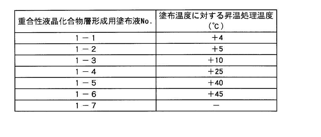
- the coating liquid for forming a polymerizable liquid crystal compound layer shown below is subjected to a temperature rising process by changing the temperature of the coating liquid for forming a polymerizable liquid crystal compound layer before coating under the conditions shown in Table 1, and subsequently applied in the temperature lowering process.
- the coating liquid for forming a polymerizable liquid crystal compound layer was prepared by applying a temperature-lowering treatment to the temperature and not performing a filtration treatment in the coating liquid filtration step. 1-1 to 1-6.
- a coating liquid for forming a polymerizable liquid crystal compound layer was prepared under the same conditions except that no treatment was performed in the temperature raising step and the temperature lowering step, and the comparative polymerizable liquid crystal compound layer forming coating solution No. 1-7.
- the temperature increasing treatment time was 30 minutes
- the temperature increasing rate of the temperature increasing treatment was 1.0 ° C./min
- the temperature decreasing rate was 1.0 ° C./min.
- the nematic-isotropic liquid phase transition temperature of this polymerizable liquid crystal composition was 73 ° C.
- the prepared coating liquid for forming a polymerizable liquid crystal compound layer is applied on the prepared cellulose ester film, and a retardation layer is formed through a drying process, an alignment process, and a curing process.
- An optical compensation film having a retardation layer was prepared and 101 to 107.
- the coating liquid for forming the polymerizable liquid crystal compound layer was used for coating immediately after being lowered to the coating temperature in the temperature lowering process.
- the prepared coating liquid for forming a polymerizable liquid crystal compound layer was applied on a cellulose ester film cut to a width of 1325 mm with an extrusion die coater at a coating liquid temperature of 22 ° C. at the time of application to form a coating film.
- the conveyance speed of the cellulose ester film was 10 m / min.
- This coating film is conveyed to a drying process, and the solvent of the coating film is evaporated. The temperature was adjusted so that the coating surface temperature was equal to or higher than the isotropic phase transition temperature before the drying process was completed.
- the film thickness of the polymerizable liquid crystal compound layer after drying was 1.65 ⁇ m.
- the film thickness of the polymerizable liquid crystal compound layer is a value measured using an optical interference film thickness meter FE-3000 (manufactured by Otsuka Electronics Co., Ltd.).
- the rod-shaped polymerizable liquid crystal compound in the polymerizable liquid crystal compound layer before curing is irradiated by irradiating ultraviolet rays so that the integrated light quantity becomes 250 mJ / cm 2 at an output of 160 W / cm with a high pressure mercury lamp with an oxygen concentration of 0.2%.
- a polymerizable liquid crystal compound layer (retardation layer) that was cured to fix the alignment state was obtained.
- the film thickness of the polymerizable liquid crystal compound layer (retardation layer) was 1.4 ⁇ m.
- an optical interference film thickness meter FE-3000 manufactured by Otsuka Electronics Co., Ltd.
- Each optical compensation film No. Table 2 shows the results obtained by measuring surface roughness, alignment defects, and haze as substitute characteristics for surface roughness by the methods shown below and evaluating according to the evaluation ranks shown below.
- Measuring method of surface roughness 10m, 100m, 500m to 1m were sampled from the start of sample application, 10 points per sample were measured with a surface roughness meter manufactured by WYCO, and the average value was defined as the surface roughness. .
- Evaluation rank of surface roughness ⁇ Less than 1.5 nm ⁇ : 1.5 nm or more, less than 2.5 nm ⁇ : 2.5 nm or more, less than 3.5 nm ⁇ : 3.5 nm or more Measurement method of orientation defect 10 m, 100 m, and 500 m to 1 m were sampled, and the alignment defects generated in the polarizing microscope attached to each sample were counted and averaged, and converted to the number of alignment defects per unit area.
- Evaluation rank of orientation defects ⁇ : Less than 0.5 pieces / mm 2 ⁇ : 0.5 pieces / mm 2 or more, less than 1.0 pieces / mm 2 ⁇ : 1.0 piece / mm 2 or more, 1.5 pieces / mm 2 Less than mm 2 ⁇ : 1.5 pcs / mm 2 or more Haze measurement method Samples 10m, 100m, 500m to 1m from the start of sample application, and 10 points per sample were measured with a haze meter (1001DP type, NEC) Measured by Color Industries Co., Ltd.) and averaged.
- a haze meter 1001DP type, NEC
- Evaluation rank of haze ⁇ Less than 1.0 ⁇ : 1.0 or more, less than 1.5 ⁇ : 1.5 or more, less than 2.0 ⁇ : 2.0 or more
- the temperature was increased from + 5 ° C. to + 40 ° C. with respect to the temperature at the time of application, and the optical compensation film No. .
- the surface roughness, the alignment defect, and the haze all showed results superior to the comparison.
- Optical compensation film No. produced by coating using a coating liquid for forming a polymerizable liquid crystal compound layer that was heated at + 4 ° C. with respect to the temperature at the time of coating.
- No. 101 shows surface roughness, alignment defects, and haze. The result was inferior to 102-105.
- Optical compensation film No. prepared by coating using a coating liquid for forming a polymerizable liquid crystal compound layer that was heated at 45 ° C. with respect to the temperature at the time of coating.
- No. 106 shows surface roughness, alignment defects, and haze. The result was inferior to 102-105.
- Optical compensation film No. produced using a coating liquid for forming a polymerizable liquid crystal compound layer that is not subjected to a temperature rise treatment.
- No. 107 is any of the surface roughness, alignment defects, and haze of the sample No. of the present invention. The result was inferior to 102-105. The effectiveness of the present invention was confirmed.
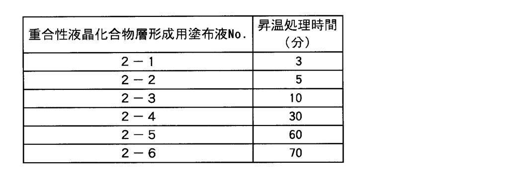
- Example 2 Production of optical compensation film >> (Preparation of coating liquid for forming a polymerizable liquid crystal compound layer) After preparing a coating liquid for forming a polymerizable liquid crystal compound layer comprising the same polymerizable liquid crystal composition as in Example 1, the temperature of the temperature raising process in the temperature raising step was changed as shown in Table 3 to form a polymerizable liquid crystal compound layer. A coating liquid for forming a polymerizable liquid crystal compound layer was prepared. From 2-1 to 2-6.
- the temperature raising treatment was performed at a temperature of 40 ° C., the temperature raising treatment at a temperature raising rate of 1.0 ° C./min, and the temperature lowering rate at 1.0 ° C./min.
- Each optical compensation film No. Table 4 shows the results obtained by measuring the alignment defects and haze as the optical characteristics and the surface roughness as the surface characteristics by the same method as in Example 1 and evaluating according to the same evaluation rank as in Example 1.
- the heating process time of the heating process is 5 minutes or more and within 60 minutes.
- Example 3 Production of optical compensation film >> (Preparation of coating liquid for forming a polymerizable liquid crystal compound layer) After preparing a coating liquid for forming a polymerizable liquid crystal compound layer comprising the same polymerizable liquid crystal composition as in Example 1, the temperature rising rate in the temperature rising step is changed as shown in Table 5 to apply for forming a polymerizable liquid crystal compound layer.
- the temperature raising treatment was performed at 40 ° C. (the temperature raising treatment temperature was + 18 ° C. with respect to the coating temperature of 22 ° C.), and the temperature lowering rate was 1.0 ° C./min.
- Each optical compensation film No. Table 6 shows the results obtained by measuring surface roughness, orientation defects, and haze in 301 to 306 in the same manner as in Example 1 and evaluating according to the same evaluation rank as in Example 1.
- the temperature rising rate of the temperature rising process is 2 ° C./min or less.
- the surface characteristics were surface roughness, and the optical characteristics were orientation defects and haze, both of which showed results superior to the comparison. The effectiveness of the present invention was confirmed.
- Example 4 Production of optical compensation film >> (Preparation of coating liquid for forming a polymerizable liquid crystal compound layer) After preparing a coating liquid for forming a polymerizable liquid crystal compound layer comprising the same polymerizable liquid crystal composition as in Example 1, the temperature decreasing rate in the temperature decreasing step was changed as shown in Table 7 to change the coating liquid for forming a polymerizable liquid crystal compound layer.
- the temperature raising treatment was performed at 40 ° C. and the temperature raising treatment time was 1.0 / min. In addition, after temperature-falling process was complete
- Each optical compensation film No. Table 8 shows the results from 401 to 406, in which surface roughness as surface characteristics, alignment defects and haze as optical characteristics were measured by the same method as in Example 1, and evaluated according to the same evaluation rank as in Example 1.
- the temperature decreasing rate in the temperature decreasing step is 2 ° C./min or less.
- the surface roughness as the characteristics and the alignment defect and haze as the optical characteristics were all superior to the comparison. The effectiveness of the present invention was confirmed.
- Example 5 Production of optical compensation film >> (Preparation of coating liquid for forming a polymerizable liquid crystal compound layer)
- a coating liquid for forming a polymerizable liquid crystal compound layer comprising the same polymerizable liquid crystal composition as in Example 1 was prepared and stored at the coating temperature until coating.
- the temperature of the heating process is 40 ° C. (the heating process temperature is + 18 ° C. with respect to the coating temperature of 22 ° C.), the heating process time is 30 / min, and the heating rate is 1.0 ° C. / Min, the temperature lowering rate of the temperature lowering step was 1.0 ° C./min.
- Each optical compensation film No. Table 9 shows the results obtained by measuring the alignment defects and haze as optical characteristics and the surface roughness as surface characteristics by the same method as in Example 1 and evaluating according to the same evaluation rank as in Example 1.
- the time until coating is set to 180 minutes or less to align as optical characteristics Defects and haze were the surface characteristics, and the surface roughness was superior to the comparison. The effectiveness of the present invention was confirmed.
- Example 6 Production of optical compensation film >> (Preparation of coating liquid for forming a polymerizable liquid crystal compound layer)
- the addition amount of the thermal polymerization inhibitor was changed as shown in Table 10.
- the temperature raising treatment temperature was 40 ° C.
- the temperature raising treatment time was 30 / min
- the temperature raising rate was 1.0 ° C./min.
- Each optical compensation film No. Table 10 shows the results obtained by measuring the alignment defects and haze as optical characteristics and the surface roughness as surface characteristics by the same method as in Example 1 and evaluating according to the same evaluation rank as in Example 1.
- a coating liquid for forming a polymerizable liquid crystal compound layer to be used for coating is prepared within the scope of the present invention, subjected to a heating step and a cooling step, and then coated to apply alignment defects and haze as optical characteristics, and surface roughness as surface characteristics. All showed results superior to the comparison. The effectiveness of the present invention was confirmed.
Landscapes
- Physics & Mathematics (AREA)
- General Physics & Mathematics (AREA)
- Optics & Photonics (AREA)
- Polarising Elements (AREA)
Abstract
重合性液晶化合物を有する位相差層を有し、表面粗れ、配向欠陥、ヘイズ上昇が少ない光学補償フィルムの製造方法を提供するため、支持体上に棒状の重合性液晶化合物を有機溶媒に溶解させた塗布液を塗布する塗布工程と、前記塗布液が塗布され前記支持体上に形成された塗膜を乾燥する乾燥工程と、前記乾燥工程の後に配向工程と、前記塗膜に対し活性放射線を照射する硬化工程とを有する光学補償フィルムの製造方法において、前記塗布工程で前記塗布液を前記支持体上に塗布する時、前記塗布液は塗布時の温度よりも+5℃から+40℃に昇温処理した後、塗布温度まで温度を下げ、前記支持体上に塗布することを特徴とする光学補償フィルムの製造方法。
Description
本発明は光学補償フィルムの製造方法に関し、更に詳しくは、棒状の重合性液晶化合物(以下、単に重合性液晶化合物とも言う)が垂直配向し、固定化された位相差層を有する光学補償フィルムの製造方法に関する。
横電界スイッチングモード型液晶表示装置は、他の液晶表示装置の液晶モード、例えばTNモードに対してはコントラスト、視野角等に優れ、又垂直配向モード(VA、MVA、PVA等)に対しては視野角等の表示性能に優れ、更に視角による輝度変化の少なさ、中間調での応答速度の落ち込みの少なさといった優れた効果から、いわゆるIPS(In Plane Switching)モード型液晶表示装置として市場に活発に提供されるようになった。IPSモード型液晶表示装置としては、いわゆるIPSモード以外に、FFS(フリンジフィールドスイッチング)モード、FLC(強誘電性液晶)モードが挙げられる。従来、IPS方式は、例えば特開2000-131700号公報に記載されている様に、液晶セル自体は補償する必要がなく、補償フィルムなしでも広い視野角が得られると言うことが知られている。
ところが、液晶表示装置に用いる偏光板自体が、クロスニコル状態で吸収軸と45°方向に視角を変化させた場合に光モレが発生し、それによって液晶表示装置の周辺コントラストが低下してしまう現象が起こっている。光モレが発生する原因の1つに液晶化合物の不均一な配向が挙げられる。そこで、例えば、特開2006-126770号公報、特開2005-31626号公報には、光学フィルムを偏光板に積層させて、偏光板の光モレを抑える形が開示されている。しかし、これらの方法は、ロールトゥーロールでの偏光板化が難しく、又粘着層や接着層を介して複数のフィルムを貼合するため、手間とコストが掛かり、更に透過率の低下や偏光板の厚膜化と言う問題が起こってしまう。
又、液晶ディスプレイが大型化するに従い、広視野角化への要求が大きくなっており、その対応として液晶セルの形式に種々の手法が提案されている。例えば広視野角化として特開2005-309379号公報に、垂直配向した棒状液晶化合物を有する位相差層を設けた光学補償フィルムを使用した偏光板、及び特開2005-265889号公報に、リターデーション上昇剤を入れた支持体に棒状液晶化合物を垂直配向させて固めた位相差層を設けた光学補償フィルムを使用した偏光板を使用することで偏光板の光モレ、広視野角化に対して有効な技術が開示されている。
又、棒状液晶化合物の配向の安定性により光モレ、広視野角化に対する効果が影響するため、更に棒状液晶化合物を垂直に配向させる技術が検討されてきた。
例えば、重合性液晶化合物が液晶規則性を発現する温度以上に加熱した後、重合性液晶化合物の液晶転移点以下の温度になるまで水冷方式等で冷却した冷却板、冷却ローラの接触による冷却、冷風の吹き付けによる方法が知られている(例えば、特許文献1参照。)。
支持体上に重合性液晶化合物を含む塗布液を塗布し、液晶化合物層を形成した後、液晶化合物層を乾燥した後に、液晶転移温度以上の温度で前記液晶化合物を加熱し配向させ、紫外線を照射して配向を固定した後、更に前記光学異方性層を加熱する方法が知られている(例えば、特許文献2参照。)。
しかしながら、特許文献1、特許文献2に記載の技術は、棒状の重合性液晶化合物を配向させるには有効な方法であるが、表面粗れ、配向欠陥、ヘイズ上昇が生じることに対して不十分であることが判った。
この様なことから重合性液晶化合物を有する位相差層を有し、表面粗れ、配向欠陥、ヘイズ上昇が少ない光学補償フィルムの製造方法の開発が望まれている。
本発明は、上記状況に鑑みなされたものであり、その目的は重合性液晶化合物を有する位相差層を有し、表面粗れ、配向欠陥、ヘイズ上昇が少ない光学補償フィルムの製造方法を提供することである。
本発明の上記目的は、下記の構成により達成された。
1.支持体上に棒状の重合性液晶化合物を有機溶媒に溶解させた塗布液を塗布する塗布工程と、前記塗布液が塗布され前記支持体上に形成された塗膜を乾燥する乾燥工程と、前記乾燥工程の後に配向工程と、前記塗膜に対し活性放射線を照射する硬化工程とを有する光学補償フィルムの製造方法において、
前記塗布工程で前記塗布液を前記支持体上に塗布する時、
前記塗布液は塗布時の温度よりも+5℃から+40℃に昇温処理した後、塗布温度まで温度を下げ、前記支持体上に塗布することを特徴とする光学補償フィルムの製造方法。
前記塗布工程で前記塗布液を前記支持体上に塗布する時、
前記塗布液は塗布時の温度よりも+5℃から+40℃に昇温処理した後、塗布温度まで温度を下げ、前記支持体上に塗布することを特徴とする光学補償フィルムの製造方法。
2.前記昇温処理の温度が、棒状の重合性液晶化合物の等方相転移温度以下であることを特徴とする前記1に記載の光学補償フィルムの製造方法。
3.前記昇温処理の時間が5分以上、60分以下であることを特徴とする前記1又は2に記載の光学補償フィルムの製造方法。
4.前記昇温処理の昇温速度が2℃/分以下であることを特徴とする前記1から3の何れか1項に記載の光学補償フィルムの製造方法。
5.前記昇温処理をした後、塗布液を塗布温度まで温度を下げる時の降温速度が2℃/分以下であることを特徴とする前記1から4の何れか1項に記載の光学補償フィルムの製造方法。
6.前記塗布液は熱重合禁止剤を棒状の重合性液晶化合物に対して、0.001質量%から2.0質量%含むことを特徴とする前記1から5の何れか1項に記載の光学補償フィルムの製造方法。
7.前記昇温処理した塗布液を濾過処理した後に塗布することを特徴とする前記1から6の何れか1項に記載の光学補償フィルムの製造方法。
8.前記昇温処理をした後に塗布するまでの時間が180分以下であることを特徴とする前記7に記載の光学補償フィルムの製造方法。
重合性液晶化合物を有する位相差層を有し、表面粗れ、配向欠陥、ヘイズ上昇が少ない光学補償フィルムの製造方法を提供することが出来た。
本発明の実施の形態を以下、図1、図2を参照しながら説明するが、本発明はこれに限定されるものではない。
図1は光学補償フィルムを用いた液晶表示装置の構成を示す概略図である。図1(a)は視認側偏光板に位相差層を有する光学補償フィルムを用いた液晶表示装置の構成を示す概略図である。図1(b)はバックライト側偏光板に位相差層を有する光学補償フィルムを用いた液晶表示装置の構成を示す概略図である。
図1(a)に示される液晶表示装置に付き説明する。図中、1aは液晶表示装置を示す。液晶表示装置1aは、視認側偏光板102と、バックライト側偏光板103との間に挟持された液晶セル101とを有する構成となっている。液晶セル101は、ガラス基板101aとガラス基板101bとの間に挟持された液晶層101cとを有する構成となっている。
視認側偏光板102は視認側(本図の上部を示す)より第1の保護フィルム102aと液晶セル101側に重合性液晶化合物の配向を固定化した位相差層102cを有する第2の保護フィルム102bとに挟持された第1の偏光膜102dとを有する構成となっている。尚、位相差層102cを有する第2の保護フィルム102bを光学補償フィルムと言う。
バックライト側偏光板103は第3の保護フィルム103aと第4の保護フィルム103bとに挟持された第2の偏光膜103cとを有する構成となっている。尚、位相差層102cは第1の偏光膜102dと第2の保護フィルム102bとの間に配置されてもよい。第2の保護フィルム102bの面内遅相軸b(図中の矢印方向)と液晶層101cの配向方向c(図中の矢印方向)は平行である。偏光膜の偏光透過軸a(図中の矢印方向)、ガラス基板のラビング軸d(図中の矢印方向)は図で示す方向にある。
図1(b)に示される液晶表示装置に付き説明する。図中、1bは液晶表示装置を示す。液晶表示装置1bは、視認側偏光板102′と、バックライト側偏光板103′との間に挟持された液晶セル101′とを有する構成となっている。液晶セル101′は、ガラス基板101′aとガラス基板101′bとの間に挟持された液晶層101′cとを有する構成となっている。
視認側偏光板102′は視認側(本図の上部側を示す)より第4の保護フィルム102′aと第3の保護フィルム102′bとに挟持された第2の偏光膜102′cとを有する構成となっている。バックライト側偏光板103′は液晶セル101′側に棒状液晶化合物の配向を固定化した位相差層103′cを有する第2の保護フィルム103′aと第1の保護フィルム103′bとに挟持された第1の偏光膜103′dとを有する構成となっている。位相差層103′cを有する第2の保護フィルム103′aを光学補償フィルムと言う。尚、位相差層103′cは第1の偏光膜103′dと第2の保護フィルム103′aの間に配置されてもよい。
第2の保護フィルム103′aの面内遅相軸b(図中の矢印方向)と液晶層101′cの配向方向c(図中の矢印方向)は直交である。偏光膜の偏光透過軸a(図中の矢印方向)、ガラス基板のラビング軸d(図中の矢印方向)は図で示す方向にある。本発明は本図に示される光学補償フィルムの製造方法に関するものである。
本発明の光学補償フィルムの製造方法に係わる光学補償フィルムは、重合性液晶化合物の溶液を樹脂フィルム基材上に塗布し、乾燥と熱量付与処理と配向工程を経て、重合性液晶化合物の配向を活性放射線硬化もしくは熱重合などで固定化を行い、垂直配向した重合性液晶化合物による位相差層を有することが特徴である。尚、垂直配向とは、得られた位相差層の光学位相差を評価するために、偏光顕微鏡を用いて評価する時、位相差層をクロスニコル偏光膜の間に挟んだ場合に黒色に見え、クロスニコル偏光膜の間で位相差層を傾けた場合に白色に見えるものを垂直配向しているものと定義する。位相差層を形成する際には、いわゆる垂直配向膜を用いてもよく、垂直配向膜として特に制限はないが、液晶材料自身が空気界面で垂直配向する場合で、その配向規制力が空気界面と反対の界面まで及ぶ場合には該配向膜は特に必要ではなく、構成が簡素化出来る観点からもその方が好ましい。垂直配向膜を使用する場合は、特開2005-148473号公報等に記載されている(メタ)アクリル系ブロックポリマーを含有するブロックポリマー組成物の架橋体からなる配向膜等を用いることも好ましい。
本発明の光学補償フィルムの製造方法に係る光学補償フィルムの位相差層は、リターデーションRoが0nmから10nm、リターデーションRtが-100nmから-400nmの範囲にある垂直配向した重合性液晶化合物による位相差層であることが好ましい。更に、Roは0nmから5nmの範囲がより好ましい。該位相差層を上記範囲とするためには、位相差層の膜厚制御、活性放射線照射、硬化時の温度、チルト角制御、及び支持体と空気界面でのプレチルト角の制御を行うことが好ましい。
尚、Roとは面内リターデーションを示し、Rtとは厚み方向リターデーションを示す。リターデーションRo、Rtは下記式により求められる。
式(i) Ro=(nx-ny)×d
式(ii) Rt=((nx+ny)/2-nz)×d
(式中、nxは位相差層面内の遅相軸方向の屈折率、nyは位相差層面内の進相軸方向の屈折率、nzは位相差層の厚み方向の屈折率(屈折率は23℃、55%RHの環境下、波長590nmで測定)、dは位相差層の厚さ(nm)を表す。)
測定には自動複屈折計KOBURA・21ADH(王子計測器(株)製)を用いて、23℃、55%RHの環境下で、波長が590nmにおいて測定した。
式(ii) Rt=((nx+ny)/2-nz)×d
(式中、nxは位相差層面内の遅相軸方向の屈折率、nyは位相差層面内の進相軸方向の屈折率、nzは位相差層の厚み方向の屈折率(屈折率は23℃、55%RHの環境下、波長590nmで測定)、dは位相差層の厚さ(nm)を表す。)
測定には自動複屈折計KOBURA・21ADH(王子計測器(株)製)を用いて、23℃、55%RHの環境下で、波長が590nmにおいて測定した。
光学補償フィルムは非常に要求性能が厳しく少しの塗布故障(欠陥)でも光学特性に大きな影響を与えることがある。本発明は、塗布前の重合性液晶化合物層形成用塗布液を昇温処理することで表面粗れ、配向欠陥、ヘイズ上昇が少ない光学補償フィルムを製造する方法に関するものである。次に、本発明の光学補償フィルムの製造方法に付き説明する。
図2は光学補償フィルムの製造工程の模式図である。
図中、2は製造工程を示す。製造工程2は、支持体としての樹脂フィルム供給工程201と、塗布工程202と、乾燥工程203と、配向工程204と、硬化工程205と、回収工程206とを順番に有している。
樹脂フィルム供給工程201はロール状に巻かれた樹脂フィルム3の繰り出し装置(不図示)を使用し、塗布工程202に樹脂フィルム3を供給する様になっている。
塗布工程202は樹脂フィルム3を保持するバックロール202aと、塗布装置202bと、塗布液調製装置202cとを使用している。
塗布液調製装置202cは、塗布液調製タンク202c1と、塗布液昇温装置202c2と、塗布液降温装置202c3と、塗布液濾過装置202c4を有している。尚、塗布液濾過装置202c4は必要に応じて使用することが可能となっている。
塗布液調製タンク202c1で調製される塗布液は使用する際には、重合性液晶化合物に対して熱重合禁止剤を、塗布液昇温装置での昇温処理時の重合反応の抑制、光学フィルムの作製時の重合反応等を考慮し、0.001質量%から2.0質量%添加することが好ましい。
塗布液昇温装置202c2は、塗布液中の各素材を活性化させ液晶分子同士、その他軟凝集等が起きている状態をバラバラにすることで塗布組成物中の状態を均一にするため塗布液を昇温処理するために配設されている。塗布液の液組成物を均一にすることで塗布・乾燥での膜も均一になりその後配向工程を経て硬化させた膜も均一な膜を得ることが可能となる。
塗布液調製タンク202c1で調製された重合性液晶化合物層形成用塗布液(以下、単に塗布液とも言う)は塗布液昇温装置202c2で、塗布時の温度よりも+5℃から+40℃に昇温処理される。
昇温処理の温度が+5℃未満の場合、塗布時の液温に対して差が少なく、塗布液の組成物を均一化する効果が得られないことがあるため好ましくない。
昇温処理の温度が+40℃を超える場合、液晶分子の活性化が上がりすぎて降温時に再凝集が生じる、固形分濃度が変化し不均一が解消されないなどの懸念があり好ましくない。
昇温処理の温度は、液晶分子へのショック、熱重合反応、相転移による乱れ等を考慮し、棒状の重合性液晶化合物の等方相転移温度以下であることが好ましい。
塗布液昇温装置202c2で昇温処理する時間は、塗布液昇温装置202c2で、塗布時の温度よりも+5℃から+40℃に昇温した後の処理する時間を言い、塗布液組成物の均一性、液の安定性等を考慮し、5分以上、60分以下であることが好ましい。更に、10分以上、30分以下がより好ましい。
塗布液昇温装置202c2で昇温処理する時の昇温速度は、重合性液晶化合物の相状態変化に重合性液晶分子が連動出来ずに逆に凝集、急激な温度変化によるショック等を考慮し、2℃/分以下であることが好ましい。より好ましくは0.1℃/分から2℃/分である。
昇温する手段は特に限定はなく、例えば釜にジャケット、ヒーターなどを設け加温する方式等が挙げられる。
塗布液昇温装置202c2で、塗布温度よりも+5℃から+40℃に昇温処理された塗布液は、塗布液降温装置202c3で塗布温度まで温度が下げられる。
塗布液を塗布温度まで温度を下げる時の降温速度は、重合性液晶化合物の相状態変化に重合性液晶分子が連動出来ず逆に凝集、急激な温度変化によるショック等を考慮し、2℃/分以下であることが好ましい。より好ましくは0.1℃/分から2℃/分である。
塗布液昇温装置202c2での昇温、塗布液降温装置202c3で塗布時の温度まで温度を下げられた塗布液は、前工程からの持ち込み異物、再凝集が発生する懸念がある場合、塗布液濾過装置202c4で濾過することが好ましい。
塗布液濾過装置202c4としては特に限定はなく、例えば、カートリッジフィルター、メンブレンフィルター、ステンレスカートリッジフィルター等が挙げられる。塗布液濾過装置202c4に使用する濾過材としては、カートリッジフィルター、メンブレンフィルター、ステンレスカートリッジフィルターであれば特に限定はなく、例えばTFPシリーズ(ヤマシンフィルタ株式会社)、TCFタイプ(ADVANTEC)等が挙げられる。
塗布液降温装置202c3で塗布時の温度まで温度を下げられた塗布液は、直接又は必要に応じて塗布液濾過装置202c4で濾過処理し、塗布装置202bに供給される。本図は塗布液濾過装置202c4で濾過処理した塗布液を直接、塗布装置202bに供給する場合を示してあるが、一旦貯留タンクに蓄えた後に塗布装置202bに供給する方式であっても構わない。一旦、貯留タンク(不図示)に蓄えた後に塗布装置202bに供給する場合の塗布液の備蓄時間は、塗布液の組成物の凝集、均一性、経時劣化、停滞安定生等を考慮し、120分以下であることが好ましい。尚、昇温処理後、貯留タンク(不図示)に移送する迄に要した時間は60分である。貯留タンク(不図示)には塗布液の温度を塗布温度に保持しておくための保持手段及び攪拌手段を配設しておくことが好ましい。
塗布装置202bにより、塗布液を樹脂フィルム3の上に塗布し、重合性液晶化合物塗膜(以下、単に塗膜とも言う)が形成される。
塗布装置202bとしては特に限定はなく、例えば、ロールコート法、プリント法、浸漬引き上げ法、ダイコート法、キャスティング法、バーコート法、ブレードコート法、スプレーコート法、グラビアコート法、リバースコート法、スライド法、カーテン法等が挙げられるが、公知の塗布方法であれば使用可能である。
乾燥工程203では塗布工程202から送られて来る樹脂フィルム3の上に形成された塗膜の溶媒を蒸発させ重合性液晶化合物層を形成する工程である。
重合性液晶化合物は低温から高温に温度を変化することにより、重合性液晶化合物の分子は結晶相(クリスタル相)、液晶相(ネマチック相)、等方相(イソトロピック相)に相変化することが知られている。このことから乾燥工程203の後半に温度を高くした領域を配設することが好ましい。温度を高くした領域を通すことで、重合性液晶化合物の分子は等方相(イソトロピック相)状態となり安定となる。
溶媒を除去する方法としては、例えば、風乾、加熱除去、もしくは減圧除去、更にはこれらを組み合わせる方法等により行われる。
乾燥工程203の終了後は速やかに配向工程204に移行することが好ましく、具体的には乾燥工程203の処理終了後10秒以内に配向工程204の冷却ロール204aによる降温過程に移行することが好ましい。乾燥工程203の終了後、温度が高い状態を長く維持していると等方相から液晶相になる温度に移動しても重合性液晶化合物層中液晶分子の動きが遅くなり垂直配向するのに要する時間が長くなってしまうことがある。
重合性液晶化合物は、光学異方性の面から液晶相(ネマチック相)状態で固定化することが好ましいことが知られており、配向工程204は等方相(イソトロピック相)から液晶相(ネマチック相)状態にする工程であり、冷却されている区間を有している。
冷却手段の一例として冷却ロールが挙げられる。本図は配向工程204に冷却ロール204aを用いた場合を示している。乾燥工程203から搬送されてくる重合性液晶化合物層を形成した樹脂フィルムの温度を下げることで重合性液晶化合物を垂直配向させる工程である。尚、冷却ロール204aは複数本を配設することも可能である。
冷却ロール204aを冷却する方法は特に限定されないが、例えば冷水を流す方法、ペルチェ素子を使用した冷却手段を使用する方法等が挙げられる。
冷却ロール204aにより降温し、重合性液晶化合物を垂直配向した状態で硬化工程205で固定化するに当たり、冷却ロール204aから硬化工程205までの温度履歴により重合性液晶化合物の配向状態が異なる。乾燥工程203以降から硬化工程までの環境は、重合性液晶化合物の配向状態を考慮し、15℃以上、40℃以下に10秒から300秒置くことが好ましい。
尚、本図では樹脂フィルムの温度を下げる手段として冷却ロールを使用した場合を示したが、基材の温度を下げる手段は特に限定はなく、例えば冷風の吹き付けによる冷却ゾーンであってもよい。
硬化工程205は垂直配向した重合性液晶化合物層を硬化し重合性液晶化合物の垂直配向を固定化することで、位相差層としての機能を付与する工程である。205aは紫外線照射装置を示す。
硬化工程205では、重合性液晶化合物を硬化させるためのエネルギーが与えられ、熱エネルギーでもよいが、重合を起こさせる能力がある電離放射線の照射によって行う。必要であれば重合性液晶化合物内に重合開始剤が含まれていてもよい。電離放射線としては、重合性液晶化合物を重合させることが可能な放射線であれば特に限定されるものではないが、装置の容易性等の観点から紫外光が使用され、波長が250nmから450nmであり、もっと好ましくは300nmから400nmの波長の紫外線である。
本発明においては、紫外線(UV)を活性放射線として照射し、紫外線で重合開始剤からラジカルを発生させ、ラジカル重合を行わせる方法が好ましい。活性放射線としてUVを用いる方法は、既に確立された技術であることから、用いる重合開始剤を含めて、本発明への応用が容易であるからである。
この紫外線を照射するための光源としては、低圧水銀ランプ(殺菌ランプ、蛍光ケミカルランプ、ブラックライト)、高圧放電ランプ(高圧水銀ランプ、メタルハライドランプ)、もしくはショートアーク放電ランプ(超高圧水銀ランプ、キセノンランプ、水銀キセノンランプ)等を挙げることが出来る。中でもメタルハライドランプ、キセノンランプ、高圧水銀ランプ灯等の使用が推奨される。照射強度は、液晶層を形成している重合性液晶化合物の組成や光重合開始剤の多寡によって適宜に調整すればよい。
活性放射線の照射による硬化工程は、上述した重合性液晶化合物層を形成する工程における処理温度、即ち重合性液晶化合物が液晶相(ネマチック相)となる温度条件で行ってもよく、又液晶相(ネマチック相)となる温度より低い温度で行ってもよい。液晶相温度以下とは結晶相領域にするとのことを意味するが、液晶分子は温度低下速度に追従出来ず遅れるためある程度の時間であれば結晶相とはならず液晶分子は液晶相状態にすることが出来る。但し、液晶が結晶化する温度まで下げてはならない。
本図に示す様に、塗布する前に塗布液を塗布時の温度よりも+5℃から+40℃に昇温処理した後、塗布時の温度まで温度が下げ塗布することで次の効果が挙げられる。
1)塗布液中の組成物が均一化され、塗布・乾燥での膜も均一になりその後配向工程を経て硬化させた塗膜の厚さ、塗膜面も均一となり、安定した位相差層が形成することが可能となった。
2)塗布液の組成物が不均一に伴う重合性液晶化合物の部分的な配向欠陥、表面粗さ、ヘイズ上昇が少ない光学特性も良好な光学補償フィルムの製造が可能となった。
3)配向欠陥、表面粗さ、ヘイズ上昇がない位相差層を有した位相差フィルムの安定生産が可能となった。
1)塗布液中の組成物が均一化され、塗布・乾燥での膜も均一になりその後配向工程を経て硬化させた塗膜の厚さ、塗膜面も均一となり、安定した位相差層が形成することが可能となった。
2)塗布液の組成物が不均一に伴う重合性液晶化合物の部分的な配向欠陥、表面粗さ、ヘイズ上昇が少ない光学特性も良好な光学補償フィルムの製造が可能となった。
3)配向欠陥、表面粗さ、ヘイズ上昇がない位相差層を有した位相差フィルムの安定生産が可能となった。
次に本発明の光学補償フィルムの製造方法に係わる材料に付き説明する。
(棒状の重合性液晶化合物)
棒状の重合性液晶化合物は、所定の活性放射線を照射することにより重合させることが出来、重合させた状態では配向状態は固定化されるようになっている。棒状の重合性液晶化合物としては、重合性液晶モノマー、重合性液晶オリゴマー、もしくは重合性液晶ポリマーの何れかを用いることが出来、相互に混合して用いることも出来る。棒状の重合性液晶化合物は、配向状態を固定化することが可能であるので、重合性液晶化合物の配向を低温で容易に行うことが可能であり、且つ使用に際しては配向状態が固定化されているので、温度等の使用条件に係わらず使用することが出来る。
棒状の重合性液晶化合物は、所定の活性放射線を照射することにより重合させることが出来、重合させた状態では配向状態は固定化されるようになっている。棒状の重合性液晶化合物としては、重合性液晶モノマー、重合性液晶オリゴマー、もしくは重合性液晶ポリマーの何れかを用いることが出来、相互に混合して用いることも出来る。棒状の重合性液晶化合物は、配向状態を固定化することが可能であるので、重合性液晶化合物の配向を低温で容易に行うことが可能であり、且つ使用に際しては配向状態が固定化されているので、温度等の使用条件に係わらず使用することが出来る。
棒状の重合性液晶化合物としては、例えば、Makromol.Chem.,190巻、2255頁(1989年)、Advanced Materials 5巻、107頁(1993年)、米国特許第4683327号明細書、同5622648号明細書、同5770107号明細書、国際公開第95/22586号明細書、同95/24455号明細書、同97/00600号明細書、同98/23580号明細書、同98/52905号明細書、特開平1-272551号公報、同6-16616号公報、同7-110469号公報、同11-80081号公報、特開2001-328973号公報、特開2002-30042号公報、特開2004-240188号公報、特開2005-99236号公報、特開2005-99237号公報、特開2005-121827号公報、特開2005-55486号公報、特開2005-309379号公報、特開2005-265889号公報、特開2006-227630号公報等に記載されている化合物が挙げられる。
(光重合開始剤)
棒状の重合性液晶化合物に加え、必要に応じて光重合開始剤を用いてもよい。電子線照射により重合性液晶化合物を重合させる際には、光重合開始剤が不要な場合があるが、一般的に用いられている。例えば紫外線(UV)照射による硬化の場合においては、通常光重合開始剤が重合促進のために用いられるからである。
棒状の重合性液晶化合物に加え、必要に応じて光重合開始剤を用いてもよい。電子線照射により重合性液晶化合物を重合させる際には、光重合開始剤が不要な場合があるが、一般的に用いられている。例えば紫外線(UV)照射による硬化の場合においては、通常光重合開始剤が重合促進のために用いられるからである。
光重合開始剤としては、ベンジル(ビベンゾイルとも言う)、ベンゾインイソブチルエーテル、ベンゾインイソプロピルエーテル、ベンゾフェノン、ベンゾイル安息香酸、ベンゾイル安息香酸メチル、4-ベンゾイル-4′-メチルジフェニルサルファイド、ベンジルメチルケタール、ジメチルアミノメチルベンゾエート、2-n-ブトキシエチル-4-ジメチルアミノベンゾエート、p-ジメチルアミノ安息香酸イソアミル、3,3′-ジメチル-4-メトキシベンゾフェノン、メチロベンゾイルフォーメート、2-メチル-1-(4-(メチルチオ)フェニル)-2-モルフォリノプロパン-1-オン、2-ベンジル-2-ジメチルアミノ-1-(4-モルフォリノフェニル)-ブタン-1-オン、1-(4-ドデシルフェニル)-2-ヒドロキシ-2-メチルプロパン-1-オン、1-ヒドロキシシクロヘキシルフェニルケトン、2-ヒドロキシ-2-メチル-1-フェニルプロパン-1-オン、1-(4-イソプロピルフェニル)-2-ヒドロキシ-2-メチルプロパン-1-オン、2-クロロチオキサントン、2,4-ジエチルチオキサントン、2,4-ジイソプロピルチオキサントン、2,4-ジメチルチオキサントン、イソプロピルチオキサントン、もしくは1-クロロ-4-プロポキシチオキサントン等を挙げることが出来る。光重合開始剤の添加量としては、一般的には0.01%から20%が好ましく、より好ましくは0.1%から10%であり、更に好ましくは0.5%から5%の範囲で、重合性液晶化合物に添加することが出来る。尚、光重合開始剤の他に、本発明の目的が損なわれない範囲で増感剤を添加することも可能である。
(熱重合禁止剤)
熱重合防止剤としては、ハイドロキノン、ハイドロキノンモノメチルエーテル、p-メトキシフェノール、ジ-t-ブチル-p-クレゾール、ピロガロール、t-ブチルカテコール、ベンゾキノン、ピクリン酸、塩化銅、メチルハイドロキノン、メトキノン、4,4′-チオビス(3-メチル-6-t-ブチルフェノール)、2,2′-メチレンビス(4-メチル-6-t-ブチルフェノール)、ジフェニルピクリルヒドラジド、N-ニトロソフェニルヒドロキシアミン第一セリウム塩等が挙げられる。
熱重合防止剤としては、ハイドロキノン、ハイドロキノンモノメチルエーテル、p-メトキシフェノール、ジ-t-ブチル-p-クレゾール、ピロガロール、t-ブチルカテコール、ベンゾキノン、ピクリン酸、塩化銅、メチルハイドロキノン、メトキノン、4,4′-チオビス(3-メチル-6-t-ブチルフェノール)、2,2′-メチレンビス(4-メチル-6-t-ブチルフェノール)、ジフェニルピクリルヒドラジド、N-ニトロソフェニルヒドロキシアミン第一セリウム塩等が挙げられる。
(溶媒)
塗布液の調製に使用する溶媒としては、上述した重合性液晶材料等を溶解することが可能な溶媒であり、且つ透明樹脂フィルムの性状を低下させない溶媒であれば特に限定されるものではない。具体的には、ベンゼン、トルエン、等の炭化水素類;メトキシベンゼン、ジエチレングリコールジメチルエーテル等のエーテル類;アセトン、メチルエチルケトン、メチルイソブチルケトン、シクロヘキサノン等のケトン類;酢酸エチル、エチレングリコールモノメチルエーテルアセテート、プロピレングリコールモノメチルエーテルアセテートもしくはγ-ブチロラクトン等のエステル類;2-ピロリドン、N-メチル-2-ピロリドン、ジメチルホルムアミド等のアミド系溶媒;ジクロロメタン、四塩化炭素、ジクロロエタン、テトラクロロエタン、トリトリクロロエチレン、テトラクロロエチレン等のハロゲン系溶媒;t-ブチルアルコール、ジアセトンアルコール、グリセリン、モノアセチン、エチレングリコール、トリエチレングリコール、エチレングリコールモノメチルエーテル、エチルセルソルブ等のアルコール類;フェノール、パラクロロフェノール等のフェノール類等の1種又は2種以上が使用可能である。
塗布液の調製に使用する溶媒としては、上述した重合性液晶材料等を溶解することが可能な溶媒であり、且つ透明樹脂フィルムの性状を低下させない溶媒であれば特に限定されるものではない。具体的には、ベンゼン、トルエン、等の炭化水素類;メトキシベンゼン、ジエチレングリコールジメチルエーテル等のエーテル類;アセトン、メチルエチルケトン、メチルイソブチルケトン、シクロヘキサノン等のケトン類;酢酸エチル、エチレングリコールモノメチルエーテルアセテート、プロピレングリコールモノメチルエーテルアセテートもしくはγ-ブチロラクトン等のエステル類;2-ピロリドン、N-メチル-2-ピロリドン、ジメチルホルムアミド等のアミド系溶媒;ジクロロメタン、四塩化炭素、ジクロロエタン、テトラクロロエタン、トリトリクロロエチレン、テトラクロロエチレン等のハロゲン系溶媒;t-ブチルアルコール、ジアセトンアルコール、グリセリン、モノアセチン、エチレングリコール、トリエチレングリコール、エチレングリコールモノメチルエーテル、エチルセルソルブ等のアルコール類;フェノール、パラクロロフェノール等のフェノール類等の1種又は2種以上が使用可能である。
上記した溶媒の中にあって、単独溶媒として好ましいものは、炭化水素系溶媒とグリコールモノエーテルアセテート系溶媒であり、混合溶媒として好ましいのは、エーテル類又はケトン類と、グリコール類との混合系である。
溶液の濃度は、重合性液晶材料等の溶解性や製造しようとする液晶層の膜厚に依存するため一概には規定出来ないが、通常は液晶組成物の固形分に対し1%から60%が好ましく、より好ましくは3%から40%の範囲で調整される。
(その他添加物)
本発明に用いられる液晶層形成用組成物には、本発明の目的を損なわない範囲内で、上記以外の化合物を添加することが出来る。
本発明に用いられる液晶層形成用組成物には、本発明の目的を損なわない範囲内で、上記以外の化合物を添加することが出来る。
添加出来る化合物としては、例えば、多価アルコールと1塩基酸又は多塩基酸を縮合して得られるポリエステルプレポリマーに、(メタ)アクリル酸を反応させて得られるポリエステル(メタ)アクリレート;ポリオール基と2個のイソシアネート基を持つ化合物を互いに反応させた後、その反応生成物に(メタ)アクリル酸を反応させて得られるポリウレタン(メタ)アクリレート;ビスフェノールA型エポキシ樹脂、ビスフェノールF型エポキシ樹脂、ノボラック型エポキシ樹脂、ポリカルボン酸ポリグリシジルエステル、ポリオールポリグリシジルエーテル、脂肪族もしくは脂環式エポキシ樹脂、アミンエポキシ樹脂、トリフェノールメタン型エポキシ樹脂、ジヒドロキシベンゼン型エポキシ樹脂等のエポキシ樹脂と、(メタ)アクリル酸を反応させて得られるエポキシ(メタ)アクリレート等の光重合性化合物、又はアクリル基もしくはメタクリル基を有する光重合性の液晶性化合物、特開2007-45993号公報に記載のオニウム塩、フッ化アクリレートポリマー等が挙げられる。
本発明の液晶層形成用組成物に対するこれら化合物の添加量は、本発明の目的が損なわれない範囲で選択され、一般的には、本発明の液晶層形成用組成物の40%以下であることが好ましく、より好ましくは20%以下である。
これらの化合物の添加により、本発明における液晶材料の硬化性が向上し、得られる液晶層の機械強度が増大し、又その安定性が改善される。
(重合性液晶化合物を有機溶媒に溶解した塗布液に使用する界面活性剤)
重合性液晶化合物を有機溶媒に溶解した塗布液には、塗布を容易にするために界面活性剤等を加えることが出来る。添加可能な界面活性剤を例示すると、イミダゾリン、第四級アンモニウム塩、アルキルアミンオキサイド、ポリアミン誘導体等の陽イオン系界面活性剤;ポリオキシエチレン-ポリオキシプロピレン縮合物、第一級或いは第二級アルコールエトキシレート、アルキルフェノールエトキシレート、ポリエチレングリコール及びそのエステル、ラウリル硫酸ナトリウム、ラウリル硫酸アンモニウム、ラウリル硫酸アミン類、アルキル置換芳香族スルホン酸塩、アルキルリン酸塩、脂肪族或いは芳香族スルホン酸ホルマリン縮合物等の陰イオン系界面活性剤;ラウリルアミドプロピルベタイン、ラウリルアミノ酢酸ベタイン等の両性系界面活性剤;ポリエチレングリコール脂肪酸エステル類、ポリオキシエチレンアルキルアミン等の非イオン系界面活性剤;パーフルオロアルキルスルホン酸塩、パーフルオロアルキルカルボン酸塩、パーフルオロアルキルエチレンオキシド付加物、パーフルオロアルキルトリメチルアンモニウム塩、パーフルオロアルキル基・親水性基含有オリゴマー、パーフルオロアルキル・親油基含有オリゴマーパーフルオロアルキル基含有ウレタン等のフッ素系界面活性剤などが挙げられる。界面活性剤の添加量は、界面活性剤の種類、液晶材料の種類、溶媒の種類、更には溶液を塗布する配向膜の種類にもよるが、通常は溶液に含まれる重合性液晶化合物の0.0001%から10%が好ましく、より好ましくは0.01%から5%であり、更に好ましくは0.1%から1%の範囲である。
重合性液晶化合物を有機溶媒に溶解した塗布液には、塗布を容易にするために界面活性剤等を加えることが出来る。添加可能な界面活性剤を例示すると、イミダゾリン、第四級アンモニウム塩、アルキルアミンオキサイド、ポリアミン誘導体等の陽イオン系界面活性剤;ポリオキシエチレン-ポリオキシプロピレン縮合物、第一級或いは第二級アルコールエトキシレート、アルキルフェノールエトキシレート、ポリエチレングリコール及びそのエステル、ラウリル硫酸ナトリウム、ラウリル硫酸アンモニウム、ラウリル硫酸アミン類、アルキル置換芳香族スルホン酸塩、アルキルリン酸塩、脂肪族或いは芳香族スルホン酸ホルマリン縮合物等の陰イオン系界面活性剤;ラウリルアミドプロピルベタイン、ラウリルアミノ酢酸ベタイン等の両性系界面活性剤;ポリエチレングリコール脂肪酸エステル類、ポリオキシエチレンアルキルアミン等の非イオン系界面活性剤;パーフルオロアルキルスルホン酸塩、パーフルオロアルキルカルボン酸塩、パーフルオロアルキルエチレンオキシド付加物、パーフルオロアルキルトリメチルアンモニウム塩、パーフルオロアルキル基・親水性基含有オリゴマー、パーフルオロアルキル・親油基含有オリゴマーパーフルオロアルキル基含有ウレタン等のフッ素系界面活性剤などが挙げられる。界面活性剤の添加量は、界面活性剤の種類、液晶材料の種類、溶媒の種類、更には溶液を塗布する配向膜の種類にもよるが、通常は溶液に含まれる重合性液晶化合物の0.0001%から10%が好ましく、より好ましくは0.01%から5%であり、更に好ましくは0.1%から1%の範囲である。
(支持体)
本発明に係わる光学補償フィルムに用いられる支持体としては、製造が容易であること、光学的に透明であること等が好ましく、特に透明樹脂フィルムであることが好ましい。又、棒状の重合性液晶化合物を有機溶媒に溶解させた塗布液を塗布する側には、下塗り層が形成されていてもよい。本発明で言う透明とは、可視光の透過率60%以上であることを指し、好ましくは80%以上であり、特に好ましくは90%以上である。
本発明に係わる光学補償フィルムに用いられる支持体としては、製造が容易であること、光学的に透明であること等が好ましく、特に透明樹脂フィルムであることが好ましい。又、棒状の重合性液晶化合物を有機溶媒に溶解させた塗布液を塗布する側には、下塗り層が形成されていてもよい。本発明で言う透明とは、可視光の透過率60%以上であることを指し、好ましくは80%以上であり、特に好ましくは90%以上である。
上記の性質を有していれば特に限定はないが、例えば、セルロースジアセテートフィルム、セルローストリアセテートフィルム、セルロースアセテートプロピオネートフィルム、セルロースアセテートブチレートフィルム等のセルロースエステル系フィルム、ポリエステル系フィルム、ポリカーボネート系フィルム、ポリアリレート系フィルム、ポリスルホン(ポリエーテルスルホンも含む)系フィルム、ポリエチレンテレフタレート、ポリエチレンナフタレート等のポリエステルフィルム、ポリエチレンフィルム、ポリプロピレンフィルム、セロファン、ポリ塩化ビニリデンフィルム、ポリビニルアルコールフィルム、エチレンビニルアルコールフィルム、シンジオタクティックポリスチレン系フィルム,ポリカーボネートフィルム、ノルボルネン系樹脂フィルム、ポリメチルペンテンフィルム、ポリエーテルケトンフィルム、ポリエーテルケトンイミドフィルム、ポリアミドフィルム、フッ素樹脂フィルム、ナイロンフィルム、ポリメチルメタクリレートフィルム、アクリルフィルム又はガラス板等を挙げることが出来る。中でもノルボルネン系樹脂フィルム、及びセルロースエステル系フィルムが好ましい。
ノルボルネン系樹脂フィルムとは、ノルボルネン構造を有する非晶性ポリオレフィンフィルムで、例えば三井石油化学(株)製のAPOや日本ゼオン(株)製のゼオネックス、JSR(株)製のARTON等がある。
本発明に係わる光学補償フィルムにおいては、これらの中でも特開2007-231157号公報、同2006-301592号公報、同2005-031614号公報、同2004-272234号公報に記載のセルロースエステル系フィルムを用いることが好ましい。市販のセルロースエステル系フィルムとしては、例えば、コニカミノルタタック KC8UX、KC4UX、KC5UX、KC8UCR3、KC8UCR4、KC8UCR5、KC8UY、KC4UY、KC12UR、KC4FR、KC8UY-HA、KC8UX-RHA(コニカミノルタオプト(株)製)等が、製造上、コスト面、透明性、密着性等の観点から好ましく用いられる。これらのフィルムは、溶融流延製膜で製造されたフィルムであっても、溶液流延製膜で製造されたフィルムであってもよい。
以下、実施例を挙げて本発明の具体的な効果を示す、本発明はこれらに限定されるものではない。
(支持体の作製)
支持体としてセルロースエステルフィルムを次ぎに示す方法で作製した。
支持体としてセルロースエステルフィルムを次ぎに示す方法で作製した。
(二酸化珪素分散液の調製)
アエロジル972V(日本アエロジル(株)製) 12質量部
(一次粒子の平均径16nm、見掛け比重90g/リットル)
エタノール 88質量部
以上をディゾルバーで30分間攪拌混合した後、マントンゴーリンで分散を行った。分散後の液濁度は200ppmであった。二酸化珪素分散液に88質量部のメチレンクロライドを攪拌しながら投入し、ディゾルバーで30分間攪拌混合し、二酸化珪素分散希釈液を調製した。
アエロジル972V(日本アエロジル(株)製) 12質量部
(一次粒子の平均径16nm、見掛け比重90g/リットル)
エタノール 88質量部
以上をディゾルバーで30分間攪拌混合した後、マントンゴーリンで分散を行った。分散後の液濁度は200ppmであった。二酸化珪素分散液に88質量部のメチレンクロライドを攪拌しながら投入し、ディゾルバーで30分間攪拌混合し、二酸化珪素分散希釈液を調製した。
(ドープ液の調製)
セルロースエステル(アセチル基置換度2.50、プロピオニル基置換度0.10、総アシル基置換度2.60) 100質量部
トリメチロールプロパントリベンゾエート 5質量部
エチルフタリルエチルグリコレート 5質量部
二酸化珪素分散希釈液 10質量部
チヌビン109(チバ・ジャパン(株)製) 1.2質量部
チヌビン171(チバ・ジャパン(株)製) 0.8質量部
メチレンクロライド 430質量部
エタノール 40質量部
上記ドープ組成物を密封容器に投入し、70℃まで加熱し、撹拌しながら、セルロースエステルを完全に溶解しドープ液を調製した。
セルロースエステル(アセチル基置換度2.50、プロピオニル基置換度0.10、総アシル基置換度2.60) 100質量部
トリメチロールプロパントリベンゾエート 5質量部
エチルフタリルエチルグリコレート 5質量部
二酸化珪素分散希釈液 10質量部
チヌビン109(チバ・ジャパン(株)製) 1.2質量部
チヌビン171(チバ・ジャパン(株)製) 0.8質量部
メチレンクロライド 430質量部
エタノール 40質量部
上記ドープ組成物を密封容器に投入し、70℃まで加熱し、撹拌しながら、セルロースエステルを完全に溶解しドープ液を調製した。
(セルロースエステルフィルムの作製)
準備したドープ液を濾過した後、33℃に温度調整しダイに送液して、ダイスリットからステンレスベルト上に幅2.5mで均一に流延した。ステンレスベルトの流延部は裏面から37℃の温水で加熱した。流延後、金属支持体上のドープ膜(ステンレスベルトに流延以降はウェブと言う)に44℃の温風を当てて乾燥させ、剥離の残留溶媒量が120質量%で剥離し、剥離の際の張力を掛けて1.1倍の縦延伸倍率となるように延伸し、次いで、残留溶媒量24%、温度135℃にてテンターでウェブ端部を把持し、幅手方向に1.2倍の延伸倍率となるように延伸した。延伸後、その幅を維持したまま数秒間保持した後、幅方向の張力を緩和させ、幅保持を解放した後に120℃で乾燥させた。以上のようにして作製した膜厚30μm、幅2.65m、長さ7500mのセルロースエステルフィルムをコアに巻き取った。
準備したドープ液を濾過した後、33℃に温度調整しダイに送液して、ダイスリットからステンレスベルト上に幅2.5mで均一に流延した。ステンレスベルトの流延部は裏面から37℃の温水で加熱した。流延後、金属支持体上のドープ膜(ステンレスベルトに流延以降はウェブと言う)に44℃の温風を当てて乾燥させ、剥離の残留溶媒量が120質量%で剥離し、剥離の際の張力を掛けて1.1倍の縦延伸倍率となるように延伸し、次いで、残留溶媒量24%、温度135℃にてテンターでウェブ端部を把持し、幅手方向に1.2倍の延伸倍率となるように延伸した。延伸後、その幅を維持したまま数秒間保持した後、幅方向の張力を緩和させ、幅保持を解放した後に120℃で乾燥させた。以上のようにして作製した膜厚30μm、幅2.65m、長さ7500mのセルロースエステルフィルムをコアに巻き取った。
尚、準備したセルロースエステルフィルムは実施例1から実施例6に使用する基材とした。
実施例1
《光学補償フィルムの作製》
(重合性液晶化合物層形成用塗布液の準備)
以下に示す重合性液晶化合物層形成用塗布液を表1に示す条件で塗布前の重合性液晶化合物層形成用塗布液を昇温工程で温度を変えて昇温処理し、引き続き降温工程で塗布温度まで降温処理し、塗布液濾過工程で濾過処理を行わず、重合性液晶化合物層形成用塗布液を準備し重合性液晶化合物層形成用塗布液No.1-1から1-6とした。尚昇温工程、降温工程で処理を行わない他は全て同じ条件で重合性液晶化合物層形成用塗布液を準備し濾過処理を行わずに比較重合性液晶化合物層形成用塗布液No.1-7とした。
《光学補償フィルムの作製》
(重合性液晶化合物層形成用塗布液の準備)
以下に示す重合性液晶化合物層形成用塗布液を表1に示す条件で塗布前の重合性液晶化合物層形成用塗布液を昇温工程で温度を変えて昇温処理し、引き続き降温工程で塗布温度まで降温処理し、塗布液濾過工程で濾過処理を行わず、重合性液晶化合物層形成用塗布液を準備し重合性液晶化合物層形成用塗布液No.1-1から1-6とした。尚昇温工程、降温工程で処理を行わない他は全て同じ条件で重合性液晶化合物層形成用塗布液を準備し濾過処理を行わずに比較重合性液晶化合物層形成用塗布液No.1-7とした。
尚、昇温処理の時間は30分、昇温処理の昇温速度が1.0℃/分、降温速度は1.0℃/分で行った。
(重合性液晶化合物の組成物の調製)
化合物A 45質量%
化合物B 45質量%
化合物C 10質量%
化合物A 45質量%
化合物B 45質量%
化合物C 10質量%

この重合性液晶組成物のネマチック-等方性液体相転移温度は73℃であった。
(重合性液晶組成物の調製)
重合性液晶化合物の組成物 99.7質量%
光重合開始剤ルシリンTPO(バスフ社製) 0.2質量%
ヒンダードアミンLS-765(三共ライフテック株式会社製)
0.1質量%
熱重合禁止剤(チバ・ジャパン製、IRGANOX1076)
0.1質量%
(重合性液晶化合物層形成用塗布液の調製)
重合性液晶組成物 33質量%
キシレン 67質量%
重合性液晶化合物の組成物 99.7質量%
光重合開始剤ルシリンTPO(バスフ社製) 0.2質量%
ヒンダードアミンLS-765(三共ライフテック株式会社製)
0.1質量%
熱重合禁止剤(チバ・ジャパン製、IRGANOX1076)
0.1質量%
(重合性液晶化合物層形成用塗布液の調製)
重合性液晶組成物 33質量%
キシレン 67質量%
(位相差層の形成)
図2に示す製造工程を使用し、準備した重合性液晶化合物層形成用塗布液を、準備したセルロースエステルフィルムの上に塗布し、乾燥工程、配向工程、硬化工程を経て位相差層を形成し位相差層を有する光学補償フィルムを作製しNo.101から107とした。
図2に示す製造工程を使用し、準備した重合性液晶化合物層形成用塗布液を、準備したセルロースエステルフィルムの上に塗布し、乾燥工程、配向工程、硬化工程を経て位相差層を形成し位相差層を有する光学補償フィルムを作製しNo.101から107とした。
(塗布)
重合性液晶化合物層形成用塗布液は降温処理工程で塗布温度に下げた後、直ちに塗布に使用した。準備した重合性液晶化合物層形成用塗布液をエクストルージョン型ダイコータにより、幅1325mmに断裁したセルロースエステルフィルム上に5μmの厚みで塗布時の塗布液温度22℃で塗布し塗膜を形成した。セルロースエステルフィルムの搬送速度は10m/minとした。
重合性液晶化合物層形成用塗布液は降温処理工程で塗布温度に下げた後、直ちに塗布に使用した。準備した重合性液晶化合物層形成用塗布液をエクストルージョン型ダイコータにより、幅1325mmに断裁したセルロースエステルフィルム上に5μmの厚みで塗布時の塗布液温度22℃で塗布し塗膜を形成した。セルロースエステルフィルムの搬送速度は10m/minとした。
(乾燥処理)
この塗膜を乾燥工程へ搬送し、塗膜の溶媒を蒸発さる。尚、乾燥工程を終了するまでに塗膜面温度が等方相転移温度以上になるように温度調整した。乾燥後の重合性液晶化合物層の膜厚は、1.65μmであった。
この塗膜を乾燥工程へ搬送し、塗膜の溶媒を蒸発さる。尚、乾燥工程を終了するまでに塗膜面温度が等方相転移温度以上になるように温度調整した。乾燥後の重合性液晶化合物層の膜厚は、1.65μmであった。
(残留溶媒量の測定方法)
乾燥した液晶層を有するセルロースエステルフィルムを10cm角に切り出し質量を測定し、その後オーブンにて110℃30分加熱し再度質量を測定した。この質量差より算出した1m2当たりの溶媒量を残留溶媒量とした。
乾燥した液晶層を有するセルロースエステルフィルムを10cm角に切り出し質量を測定し、その後オーブンにて110℃30分加熱し再度質量を測定した。この質量差より算出した1m2当たりの溶媒量を残留溶媒量とした。
重合性液晶化合物層の膜厚は、光干渉膜厚計FE-3000(大塚電子(株)製)を用いて測定した値を示す。
(配向工程)
温度30℃に制御された配向工程を1分間通過させた。
温度30℃に制御された配向工程を1分間通過させた。
(硬化工程)
酸素濃度0.2%、高圧水銀灯により160W/cmの出力で積算光量が250mJ/cm2となるように紫外線を照射して、硬化前の重合性液晶化合物層中の棒状の重合性液晶化合物を硬化させ配向状態を固定した重合性液晶化合物層(位相差層)を得た。重合性液晶化合物層(位相差層)の膜厚は1.4μmであった。膜厚測定は、光干渉膜厚計FE-3000(大塚電子(株)製)を用いた。
酸素濃度0.2%、高圧水銀灯により160W/cmの出力で積算光量が250mJ/cm2となるように紫外線を照射して、硬化前の重合性液晶化合物層中の棒状の重合性液晶化合物を硬化させ配向状態を固定した重合性液晶化合物層(位相差層)を得た。重合性液晶化合物層(位相差層)の膜厚は1.4μmであった。膜厚測定は、光干渉膜厚計FE-3000(大塚電子(株)製)を用いた。
評価
作製した各光学補償フィルムNo.101から107に付き、表面粗れの代用特性として表面粗さ、配向欠陥、ヘイズを以下に示す方法で測定し、以下に示す評価ランクに従って評価した結果を表2に示す。
作製した各光学補償フィルムNo.101から107に付き、表面粗れの代用特性として表面粗さ、配向欠陥、ヘイズを以下に示す方法で測定し、以下に示す評価ランクに従って評価した結果を表2に示す。
表面粗さの測定方法
試料の塗布開始から、10m、100m、500mから1mをサンプリングし、各試料に付き10点を、WYCO社製表面粗さ計で測定し、平均した値を表面粗さとした。
試料の塗布開始から、10m、100m、500mから1mをサンプリングし、各試料に付き10点を、WYCO社製表面粗さ計で測定し、平均した値を表面粗さとした。
表面粗さの評価ランク
◎:1.5nm未満
○:1.5nm以上、2.5nm未満
△:2.5nm以上、3.5nm未満
×:3.5nm以上
配向欠陥の測定方法
試料の塗布開始から、10m、100m、500mから1mをサンプリングし、各試料に付き偏光顕微鏡にて発生している配向欠陥をカウントし平均し、単位面積当たりの配向欠陥数に換算した。
◎:1.5nm未満
○:1.5nm以上、2.5nm未満
△:2.5nm以上、3.5nm未満
×:3.5nm以上
配向欠陥の測定方法
試料の塗布開始から、10m、100m、500mから1mをサンプリングし、各試料に付き偏光顕微鏡にて発生している配向欠陥をカウントし平均し、単位面積当たりの配向欠陥数に換算した。
配向欠陥の評価ランク
◎:0.5個/mm2未満
○:0.5個/mm2以上、1.0個/mm2未満
△:1.0個/mm2以上、1.5個/mm2未満
×:1.5個/mm2以上
ヘイズの測定方法
試料の塗布開始から、10m、100m、500mから1mをサンプリングし、各試料に付き10点を、ヘイズ計(1001DP型、日本電色工業(株)製)で測定し、平均した。
◎:0.5個/mm2未満
○:0.5個/mm2以上、1.0個/mm2未満
△:1.0個/mm2以上、1.5個/mm2未満
×:1.5個/mm2以上
ヘイズの測定方法
試料の塗布開始から、10m、100m、500mから1mをサンプリングし、各試料に付き10点を、ヘイズ計(1001DP型、日本電色工業(株)製)で測定し、平均した。
ヘイズの評価ランク
◎:1.0未満
○:1.0以上、1.5未満
△:1.5以上、2.0未満
×:2.0以上
◎:1.0未満
○:1.0以上、1.5未満
△:1.5以上、2.0未満
×:2.0以上
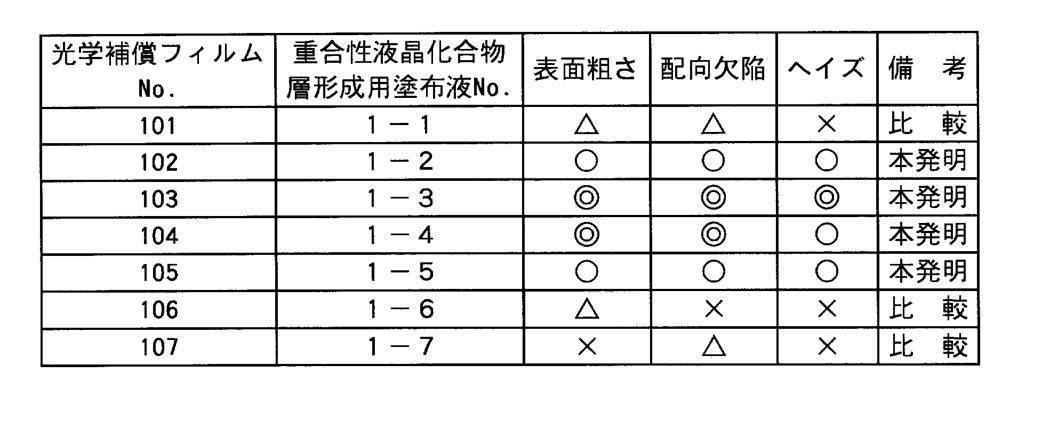
重合性液晶化合物層形成用塗布液を調整後、塗布時の温度に対して+5℃から+40℃で昇温処理し、降温処理工程で塗布温度まで下げて塗布することで作製した光学補償フィルムNo.102から105は、表面粗さ、配向欠陥、ヘイズは何れも比較よりも優れた結果を示した。
塗布時の温度に対して+4℃で昇温処理した重合性液晶化合物層形成用塗布液を使用し、塗布することで作製した光学補償フィルムNo.101は、表面粗さ、配向欠陥、ヘイズは何れも本発明の試料No.102から105に比べ劣る結果となった。
塗布時の温度に対して45℃で昇温処理した重合性液晶化合物層形成用塗布液を使用し、塗布することで作製した光学補償フィルムNo.106は、表面粗さ、配向欠陥、ヘイズは何れも本発明の試料No.102から105に比べ劣る結果となった。
昇温処理を行わない重合性液晶化合物層形成用塗布液を使用し使用し、塗布することで作製した光学補償フィルムNo.107は、表面粗さ、配向欠陥、ヘイズは何れも本発明の試料No.102から105に比べ劣る結果となった。本発明の有効性が確認された。
又、No.101から107と同じ方法塗布液を調製し、塗布前に濾過工程を通した以外はで同じ方法で光学補償フィルムを作製し評価を実施した結果、濾過なしの結果と同等の結果が得られた。
実施例2
《光学補償フィルムの作製》
(重合性液晶化合物層形成用塗布液の準備)
実施例1と同じ重合性液晶組成物からなる重合性液晶化合物層形成用塗布液を調製した後、昇温工程での昇温処理の時間を表3に示す様に変え重合性液晶化合物層形成用塗布液を調製し重合性液晶化合物層形成用塗布液No.2-1から2-6とした。
《光学補償フィルムの作製》
(重合性液晶化合物層形成用塗布液の準備)
実施例1と同じ重合性液晶組成物からなる重合性液晶化合物層形成用塗布液を調製した後、昇温工程での昇温処理の時間を表3に示す様に変え重合性液晶化合物層形成用塗布液を調製し重合性液晶化合物層形成用塗布液No.2-1から2-6とした。
尚、昇温処理の温度は40℃、昇温処理の昇温速度が1.0℃/分、降温速度は1.0℃/分で行った。尚、降温処理が終了した後、濾過処理は行わずに塗布を行った。
(位相差層の形成)
図2に示す製造工程を使用し、準備した重合性液晶化合物層形成用塗布液を、準備したセルロースエステルフィルムの上に実施例1と同じ方法で塗布し、乾燥工程、配向工程、硬化工程を経て位相差層を形成し位相差層を有する光学補償フィルムを作製しNo.201から206とした。
図2に示す製造工程を使用し、準備した重合性液晶化合物層形成用塗布液を、準備したセルロースエステルフィルムの上に実施例1と同じ方法で塗布し、乾燥工程、配向工程、硬化工程を経て位相差層を形成し位相差層を有する光学補償フィルムを作製しNo.201から206とした。
評価
作製した各光学補償フィルムNo.201から206に付き、光学特性として配向欠陥、ヘイズを、表面特性として表面粗さを実施例1と同じ方法で測定し、実施例1と同じ評価ランクに従って評価した結果を表4に示す。
作製した各光学補償フィルムNo.201から206に付き、光学特性として配向欠陥、ヘイズを、表面特性として表面粗さを実施例1と同じ方法で測定し、実施例1と同じ評価ランクに従って評価した結果を表4に示す。
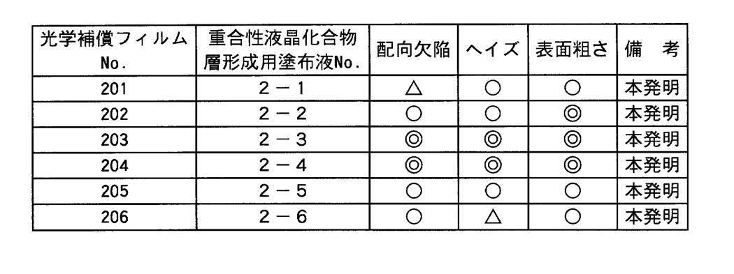
塗布に使用する重合性液晶化合物層形成用塗布液を調製後、昇温工程、降温工程で本発明の範囲で処理する際、昇温工程の昇温処理の時間を5分以上、60分以内とすることで光学特性として表面粗さ配向欠陥、ヘイズを、何れも比較よりも優れた結果を示した。本発明の有効性が確認された。
実施例3
《光学補償フィルムの作製》
(重合性液晶化合物層形成用塗布液の準備)
実施例1と同じ重合性液晶組成物からなる重合性液晶化合物層形成用塗布液を調製した後、昇温工程での昇温速度を表5に示す様に変え重合性液晶化合物層形成用塗布液を調製し重合性液晶化合物層形成用塗布液No.3-1から3-6とした。尚、昇温処理の温度は40℃(塗布温度22℃に対して昇温処理温度は+18℃となる。)、降温速度は1.0℃/分で行った。尚、降温処理が終了した後、濾過処理は行わずに塗布を行った。
《光学補償フィルムの作製》
(重合性液晶化合物層形成用塗布液の準備)
実施例1と同じ重合性液晶組成物からなる重合性液晶化合物層形成用塗布液を調製した後、昇温工程での昇温速度を表5に示す様に変え重合性液晶化合物層形成用塗布液を調製し重合性液晶化合物層形成用塗布液No.3-1から3-6とした。尚、昇温処理の温度は40℃(塗布温度22℃に対して昇温処理温度は+18℃となる。)、降温速度は1.0℃/分で行った。尚、降温処理が終了した後、濾過処理は行わずに塗布を行った。
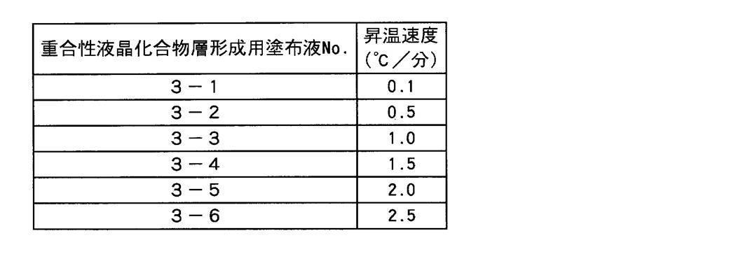
(位相差層の形成)
図2に示す製造工程を使用し、準備した重合性液晶化合物層形成用塗布液を、準備したセルロースエステルフィルムの上に実施例1と同じ方法で塗布し、乾燥工程、配向工程、硬化工程を経て位相差層を形成し位相差層を有する光学補償フィルムを作製しNo.301から306とした。
図2に示す製造工程を使用し、準備した重合性液晶化合物層形成用塗布液を、準備したセルロースエステルフィルムの上に実施例1と同じ方法で塗布し、乾燥工程、配向工程、硬化工程を経て位相差層を形成し位相差層を有する光学補償フィルムを作製しNo.301から306とした。
評価
作製した各光学補償フィルムNo.301から306に付き、表面粗さ、配向欠陥、ヘイズを実施例1と同じ方法で測定し、実施例1と同じ評価ランクに従って評価した結果を表6に示す。
作製した各光学補償フィルムNo.301から306に付き、表面粗さ、配向欠陥、ヘイズを実施例1と同じ方法で測定し、実施例1と同じ評価ランクに従って評価した結果を表6に示す。

塗布に使用する重合性液晶化合物層形成用塗布液を調製後、昇温工程、降温工程で本発明の範囲で処理する際、昇温工程の昇温速度を2℃/分以下とすることで表面特性として表面粗さ、光学特性として配向欠陥、ヘイズを、何れも比較よりも優れた結果を示した。本発明の有効性が確認された。
実施例4
《光学補償フィルムの作製》
(重合性液晶化合物層形成用塗布液の準備)
実施例1と同じ重合性液晶組成物からなる重合性液晶化合物層形成用塗布液を調製した後、降温工程での降温速度を表7に示す様に変え重合性液晶化合物層形成用塗布液を調製し重合性液晶化合物層形成用塗布液No.4-1から4-6とした。尚、昇温処理の温度は40℃、昇温処理の処理時間が1.0/分で行った。尚、降温処理が終了した後、濾過処理は行わずに塗布を行った。
《光学補償フィルムの作製》
(重合性液晶化合物層形成用塗布液の準備)
実施例1と同じ重合性液晶組成物からなる重合性液晶化合物層形成用塗布液を調製した後、降温工程での降温速度を表7に示す様に変え重合性液晶化合物層形成用塗布液を調製し重合性液晶化合物層形成用塗布液No.4-1から4-6とした。尚、昇温処理の温度は40℃、昇温処理の処理時間が1.0/分で行った。尚、降温処理が終了した後、濾過処理は行わずに塗布を行った。

(位相差層の形成)
図2に示す製造工程を使用し、準備した重合性液晶化合物層形成用塗布液を、準備したセルロースエステルフィルムの上に実施例1と同じ方法で塗布し、乾燥工程、配向工程、硬化工程を経て位相差層を形成し位相差層を有する光学補償フィルムを作製しNo.401から406とした。
図2に示す製造工程を使用し、準備した重合性液晶化合物層形成用塗布液を、準備したセルロースエステルフィルムの上に実施例1と同じ方法で塗布し、乾燥工程、配向工程、硬化工程を経て位相差層を形成し位相差層を有する光学補償フィルムを作製しNo.401から406とした。
評価
作製した各光学補償フィルムNo.401から406に付き、表面特性として表面粗さ、光学特性として配向欠陥、ヘイズを実施例1と同じ方法で測定し、実施例1と同じ評価ランクに従って評価した結果を表8に示す。
作製した各光学補償フィルムNo.401から406に付き、表面特性として表面粗さ、光学特性として配向欠陥、ヘイズを実施例1と同じ方法で測定し、実施例1と同じ評価ランクに従って評価した結果を表8に示す。

塗布に使用する重合性液晶化合物層形成用塗布液を調製後、昇温工程、降温工程で本発明の範囲で処理する際、降温工程の降温速度を2℃/分以下とすることで、表面特性として表面粗さ、光学特性として配向欠陥、ヘイズを、何れも比較よりも優れた結果を示した。本発明の有効性が確認された。
実施例5
《光学補償フィルムの作製》
(重合性液晶化合物層形成用塗布液の準備)
実施例1と同じ重合性液晶組成物からなる重合性液晶化合物層形成用塗布液を調製し、塗布するまでは塗布温度で保存した。尚、昇温処理の温度は40℃(塗布温度22℃に対して昇温処理温度は+18℃となる。)、昇温処理の処理時間が30/分、昇温速度は1.0℃/分、降温工程の降温速度1.0℃/分で行った。尚、降温処理が終了した後、濾過処理は行わずに塗布を行った。
《光学補償フィルムの作製》
(重合性液晶化合物層形成用塗布液の準備)
実施例1と同じ重合性液晶組成物からなる重合性液晶化合物層形成用塗布液を調製し、塗布するまでは塗布温度で保存した。尚、昇温処理の温度は40℃(塗布温度22℃に対して昇温処理温度は+18℃となる。)、昇温処理の処理時間が30/分、昇温速度は1.0℃/分、降温工程の降温速度1.0℃/分で行った。尚、降温処理が終了した後、濾過処理は行わずに塗布を行った。
(位相差層の形成)
図2に示す製造工程を使用し、重合性液晶化合物層形成用塗布液の昇温処理をした後に塗布するまでの時間を表9に示す様に変えて、準備したセルロースエステルフィルムの上に実施例1と同じ方法で塗布し、乾燥工程、配向工程、硬化工程を経て位相差層を形成し位相差層を有する光学補償フィルムを作製しNo.501から506とした。
図2に示す製造工程を使用し、重合性液晶化合物層形成用塗布液の昇温処理をした後に塗布するまでの時間を表9に示す様に変えて、準備したセルロースエステルフィルムの上に実施例1と同じ方法で塗布し、乾燥工程、配向工程、硬化工程を経て位相差層を形成し位相差層を有する光学補償フィルムを作製しNo.501から506とした。
評価
作製した各光学補償フィルムNo.501から506に付き、光学特性として配向欠陥、ヘイズを、表面特性として表面粗さを実施例1と同じ方法で測定し、実施例1と同じ評価ランクに従って評価した結果を表9に示す。
作製した各光学補償フィルムNo.501から506に付き、光学特性として配向欠陥、ヘイズを、表面特性として表面粗さを実施例1と同じ方法で測定し、実施例1と同じ評価ランクに従って評価した結果を表9に示す。

塗布に使用する重合性液晶化合物層形成用塗布液を調製後、昇温工程、降温工程で本発明の範囲で処理した後、塗布するまでの時間を180分以下とすることで光学特性として配向欠陥、ヘイズを、表面特性として表面粗さ何れも比較よりも優れた結果を示した。本発明の有効性が確認された。
実施例6
《光学補償フィルムの作製》
(重合性液晶化合物層形成用塗布液の準備)
実施例1と同じ重合性液晶組成物からなる重合性液晶化合物層形成用塗布液を調製する際に熱重合禁止剤の添加量を表10の様に変化させた。尚、昇温処理の温度は40℃、昇温処理の処理時間が30/分、昇温速度は1.0℃/分降温工程の降温速度1.0℃/分で行った。尚、降温処理が終了した後、濾過処理は行わずに塗布を行った。
《光学補償フィルムの作製》
(重合性液晶化合物層形成用塗布液の準備)
実施例1と同じ重合性液晶組成物からなる重合性液晶化合物層形成用塗布液を調製する際に熱重合禁止剤の添加量を表10の様に変化させた。尚、昇温処理の温度は40℃、昇温処理の処理時間が30/分、昇温速度は1.0℃/分降温工程の降温速度1.0℃/分で行った。尚、降温処理が終了した後、濾過処理は行わずに塗布を行った。
(位相差層の形成)
図2に示す製造工程を使用し、準備した重合性液晶化合物層形成用塗布液を、準備したセルロースエステルフィルムの上に実施例1と同じ方法で塗布し、乾燥工程、配向工程、硬化工程を経て位相差層を形成し位相差層を有する光学補償フィルムを作製しNo.601から607とした。
図2に示す製造工程を使用し、準備した重合性液晶化合物層形成用塗布液を、準備したセルロースエステルフィルムの上に実施例1と同じ方法で塗布し、乾燥工程、配向工程、硬化工程を経て位相差層を形成し位相差層を有する光学補償フィルムを作製しNo.601から607とした。
評価
作製した各光学補償フィルムNo.601から607に付き、光学特性として配向欠陥、ヘイズを、表面特性として表面粗さを実施例1と同じ方法で測定し、実施例1と同じ評価ランクに従って評価した結果を表10に示す。
作製した各光学補償フィルムNo.601から607に付き、光学特性として配向欠陥、ヘイズを、表面特性として表面粗さを実施例1と同じ方法で測定し、実施例1と同じ評価ランクに従って評価した結果を表10に示す。
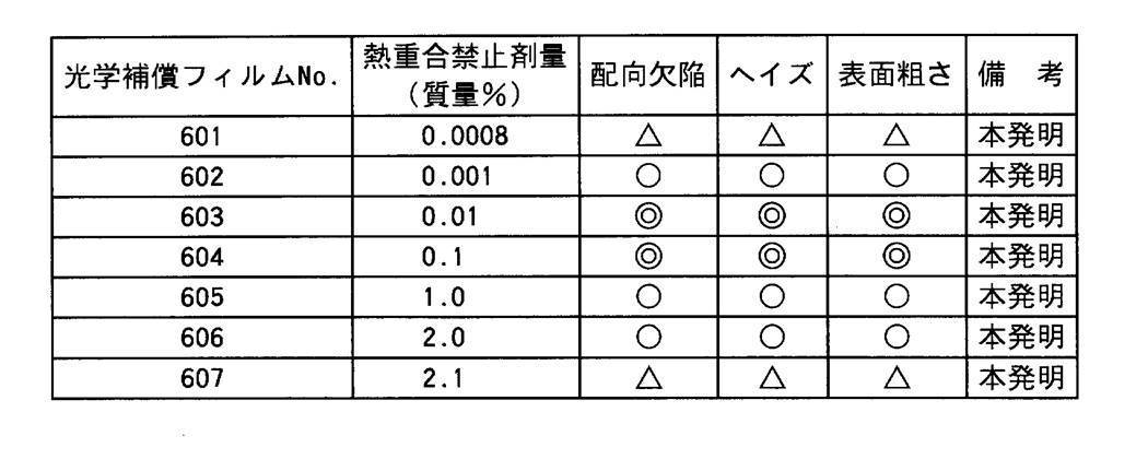
塗布に使用する重合性液晶化合物層形成用塗布液を本発明の範囲で調製し昇温工程、降温工程処理した後、塗布することで光学特性として配向欠陥、ヘイズを、表面特性として表面粗さ何れも比較よりも優れた結果を示した。本発明の有効性が確認された。
1a、1b 液晶表示装置
101、101′ 液晶セル
101a、101′a、101b、101′b ガラス基板
101c、101′c 液晶層
102、102′ 視認側偏光板
102a、103′b 第1の保護フィルム
102b、103′a 第2の保護フィルム
102c、103′c 位相差層
102d、103′d 第1の偏光膜
103、103′ バックライト側偏光板
103a、102′b 第3の保護フィルム
103b、102′a 第4の保護フィルム
103c、102′c 第2の偏光膜
2 製造装置
201 樹脂フィルム供給工程
202 塗布工程
202a バックロール
202b 塗布装置
202c 塗布液調製装置
202c1 塗布液調製タンク
202c2 塗布液昇温装置
202c3 塗布液降温装置
202c4 塗布液濾過装置
203 乾燥工程
204 配向工程
204a 冷却ロール
205 硬化工程
206 回収工程
3 樹脂フィルム
101、101′ 液晶セル
101a、101′a、101b、101′b ガラス基板
101c、101′c 液晶層
102、102′ 視認側偏光板
102a、103′b 第1の保護フィルム
102b、103′a 第2の保護フィルム
102c、103′c 位相差層
102d、103′d 第1の偏光膜
103、103′ バックライト側偏光板
103a、102′b 第3の保護フィルム
103b、102′a 第4の保護フィルム
103c、102′c 第2の偏光膜
2 製造装置
201 樹脂フィルム供給工程
202 塗布工程
202a バックロール
202b 塗布装置
202c 塗布液調製装置
202c1 塗布液調製タンク
202c2 塗布液昇温装置
202c3 塗布液降温装置
202c4 塗布液濾過装置
203 乾燥工程
204 配向工程
204a 冷却ロール
205 硬化工程
206 回収工程
3 樹脂フィルム
Claims (8)
- 支持体上に棒状の重合性液晶化合物を有機溶媒に溶解させた塗布液を塗布する塗布工程と、前記塗布液が塗布され前記支持体上に形成された塗膜を乾燥する乾燥工程と、前記乾燥工程の後に配向工程と、前記塗膜に対し活性放射線を照射する硬化工程とを有する光学補償フィルムの製造方法において、
前記塗布工程で前記塗布液を前記支持体上に塗布する時、
前記塗布液は塗布時の温度よりも+5℃から+40℃に昇温処理した後、塗布温度まで温度を下げ、前記支持体上に塗布することを特徴とする光学補償フィルムの製造方法。 - 前記昇温処理の温度が、棒状の重合性液晶化合物の等方相転移温度以下であることを特徴とする請求項1に記載の光学補償フィルムの製造方法。
- 前記昇温処理の時間が5分以上、60分以下であることを特徴とする請求項1又は2に記載の光学補償フィルムの製造方法。
- 前記昇温処理の昇温速度が2℃/分以下であることを特徴とする請求項1から3の何れか1項に記載の光学補償フィルムの製造方法。
- 前記昇温処理をした後、塗布液を塗布温度まで温度を下げる時の降温速度が2℃/分以下であることを特徴とする請求項1から4の何れか1項に記載の光学補償フィルムの製造方法。
- 前記塗布液は熱重合禁止剤を棒状の重合性液晶化合物に対して、0.001質量%から2.0質量%含むことを特徴とする請求項1から5の何れか1項に記載の光学補償フィルムの製造方法。
- 前記昇温処理した塗布液を濾過処理した後に塗布することを特徴とする請求項1から6の何れか1項に記載の光学補償フィルムの製造方法。
- 前記昇温処理をした後に塗布するまでの時間が180分以下であることを特徴とする請求項7に記載の光学補償フィルムの製造方法。
Applications Claiming Priority (2)
| Application Number | Priority Date | Filing Date | Title |
|---|---|---|---|
| JP2009-102822 | 2009-04-21 | ||
| JP2009102822 | 2009-04-21 |
Publications (1)
| Publication Number | Publication Date |
|---|---|
| WO2010122845A1 true WO2010122845A1 (ja) | 2010-10-28 |
Family
ID=43010968
Family Applications (1)
| Application Number | Title | Priority Date | Filing Date |
|---|---|---|---|
| PCT/JP2010/053636 Ceased WO2010122845A1 (ja) | 2009-04-21 | 2010-03-05 | 光学補償フィルムの製造方法 |
Country Status (1)
| Country | Link |
|---|---|
| WO (1) | WO2010122845A1 (ja) |
Citations (4)
| Publication number | Priority date | Publication date | Assignee | Title |
|---|---|---|---|---|
| JPH06332202A (ja) * | 1993-05-26 | 1994-12-02 | Canon Inc | 電子写真感光体の製造方法 |
| JPH10286511A (ja) * | 1997-02-17 | 1998-10-27 | Ricoh Co Ltd | 液体塗布装置 |
| JP2006227360A (ja) * | 2005-02-18 | 2006-08-31 | Fuji Photo Film Co Ltd | 光学補償シートおよびその製造方法、偏光板、液晶表示装置 |
| JP2007298967A (ja) * | 2006-04-03 | 2007-11-15 | Sumitomo Chemical Co Ltd | フィルムおよびフィルムの製造方法、並びにその利用 |
-
2010
- 2010-03-05 WO PCT/JP2010/053636 patent/WO2010122845A1/ja not_active Ceased
Patent Citations (4)
| Publication number | Priority date | Publication date | Assignee | Title |
|---|---|---|---|---|
| JPH06332202A (ja) * | 1993-05-26 | 1994-12-02 | Canon Inc | 電子写真感光体の製造方法 |
| JPH10286511A (ja) * | 1997-02-17 | 1998-10-27 | Ricoh Co Ltd | 液体塗布装置 |
| JP2006227360A (ja) * | 2005-02-18 | 2006-08-31 | Fuji Photo Film Co Ltd | 光学補償シートおよびその製造方法、偏光板、液晶表示装置 |
| JP2007298967A (ja) * | 2006-04-03 | 2007-11-15 | Sumitomo Chemical Co Ltd | フィルムおよびフィルムの製造方法、並びにその利用 |
Similar Documents
| Publication | Publication Date | Title |
|---|---|---|
| JP6149078B2 (ja) | 位相差フィルム、位相差フィルムの製造方法、積層体、組成物、偏光板および液晶表示装置 | |
| JP7217359B2 (ja) | 光学フィルム、円偏光板、有機エレクトロルミネッセンス表示装置 | |
| JP7187764B2 (ja) | 液晶表示装置 | |
| JP5234113B2 (ja) | 位相差フィルム、偏光板、液晶表示装置 | |
| JP5720795B2 (ja) | パターン位相差フィルム及びその製造方法 | |
| TWI718093B (zh) | 光學異向性膜 | |
| JP7282189B2 (ja) | 光学異方性層、光学フィルム、偏光板および画像表示装置 | |
| JP2001055573A (ja) | 液晶フィルム | |
| JP5282266B2 (ja) | 光学補償フィルムの製造方法 | |
| WO2021193825A1 (ja) | 光学異方性層、光学フィルム、偏光板および画像表示装置 | |
| JP2009157226A (ja) | 配向基材並びに傾斜配向位相差フィルムの製造方法 | |
| JPWO2011010551A1 (ja) | 光学異方性フィルム、偏光板及び液晶表示装置 | |
| WO2008056568A1 (en) | Polarization plate and liquid crystal display device | |
| JPWO2010110090A1 (ja) | 光学フィルム、偏光板、および液晶表示装置 | |
| JP5477186B2 (ja) | 光学異方性フィルム、偏光板及び液晶表示装置 | |
| JP2010250172A (ja) | 光学フィルム、光学フィルムの製造方法、偏光板、及び液晶表示装置 | |
| JP2009122234A (ja) | 光学補償フィルムの製造方法 | |
| JP2014186248A (ja) | 位相差フィルムの製造方法 | |
| WO2019098215A1 (ja) | 長尺液晶フィルム、長尺偏光板、画像表示装置、および、長尺液晶フィルムの製造方法 | |
| JP2010128270A (ja) | 光学補償フィルムの製造方法、光学補償フィルム、偏光板及び液晶表示装置 | |
| WO2021182248A1 (ja) | 組成物、光学フィルムの製造方法、光学フィルム | |
| JP2010085574A (ja) | 光学補償フィルムの鹸化処理方法、光学補償フィルム、偏光板、及び液晶表示装置 | |
| JP5282267B2 (ja) | 光学補償フィルムの製造方法 | |
| JP2009276442A (ja) | 1/4波長板、画像表示装置および液晶表示装置 | |
| WO2010122845A1 (ja) | 光学補償フィルムの製造方法 |
Legal Events
| Date | Code | Title | Description |
|---|---|---|---|
| 121 | Ep: the epo has been informed by wipo that ep was designated in this application |
Ref document number: 10766904 Country of ref document: EP Kind code of ref document: A1 |
|
| NENP | Non-entry into the national phase |
Ref country code: DE |
|
| 122 | Ep: pct application non-entry in european phase |
Ref document number: 10766904 Country of ref document: EP Kind code of ref document: A1 |
|
| NENP | Non-entry into the national phase |
Ref country code: JP |