WO2010116784A1 - 放射線画像検出カセッテ - Google Patents
放射線画像検出カセッテ Download PDFInfo
- Publication number
- WO2010116784A1 WO2010116784A1 PCT/JP2010/051689 JP2010051689W WO2010116784A1 WO 2010116784 A1 WO2010116784 A1 WO 2010116784A1 JP 2010051689 W JP2010051689 W JP 2010051689W WO 2010116784 A1 WO2010116784 A1 WO 2010116784A1
- Authority
- WO
- WIPO (PCT)
- Prior art keywords
- glass substrate
- base
- cassette type
- type detector
- cassette
- Prior art date
- Legal status (The legal status is an assumption and is not a legal conclusion. Google has not performed a legal analysis and makes no representation as to the accuracy of the status listed.)
- Ceased
Links
Images



Classifications
-
- G—PHYSICS
- G03—PHOTOGRAPHY; CINEMATOGRAPHY; ANALOGOUS TECHNIQUES USING WAVES OTHER THAN OPTICAL WAVES; ELECTROGRAPHY; HOLOGRAPHY
- G03B—APPARATUS OR ARRANGEMENTS FOR TAKING PHOTOGRAPHS OR FOR PROJECTING OR VIEWING THEM; APPARATUS OR ARRANGEMENTS EMPLOYING ANALOGOUS TECHNIQUES USING WAVES OTHER THAN OPTICAL WAVES; ACCESSORIES THEREFOR
- G03B42/00—Obtaining records using waves other than optical waves; Visualisation of such records by using optical means
- G03B42/02—Obtaining records using waves other than optical waves; Visualisation of such records by using optical means using X-rays
- G03B42/04—Holders for X-ray films
Definitions
- the present invention relates to a radiation image detection cassette.
- a digital radiological image detection apparatus has been used as a method for obtaining a radiographic image by irradiating a subject with radiation and detecting the radiation transmitted through the subject.
- a radiation image detection apparatus there is a so-called FPD (Flat Panel Detector).
- an FPD As an example of an FPD, a plurality of detection elements are two-dimensionally arranged on a substrate, radiation that has passed through a subject is irradiated onto a phosphor (scintillator), and visible light that is emitted according to the amount of irradiated radiation is charged. There is one that obtains a radiographic image by reading the electric charge accumulated in the photoelectric conversion element by converting into the photoelectric conversion element.
- a radiographic image can be obtained immediately after imaging.
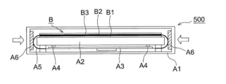
- FIG. 9 is a longitudinal sectional view of a cassette type FPD 500, and the cassette type FPD 500 shown in FIG. 9 has a structure described in Patent Document 1.
- the base A2 is built in the housing A1, and the radiation detection unit B is provided on the base A2.
- the radiation detection unit B includes a glass substrate B1 made of glass, a photoelectric conversion element B2 formed in a two-dimensional array by a semiconductor process, and a fluorescent plate B3 in which a phosphor made of a metal compound is applied to a resin plate. It is configured to be integrally laminated.
- a circuit board A3 on which electronic components for processing an electrical signal subjected to photoelectric conversion are mounted is fixed via a protrusion A4.
- the circuit board A3 and the photoelectric conversion element B2 are connected by a flexible circuit board A5.
- the cassette-type FPD 500 shown in FIG. 9 is portable and is transported to a predetermined location and used for radiographic imaging. However, the cassette-type FPD 500 is accidentally dropped while being transported to the predetermined location. In some cases, a sudden impact may be applied from the side of the cassette type FPD 500 as shown by an arrow in FIG. If no measures are taken against this impact, when a sudden impact is applied to the cassette-type FPD 500, the base A2 or the like inside the housing A1 contacts the inside of the housing A1, for example, The glass substrate B1 provided on the table A2 will be damaged.
- the cassette type FPD 500 described in Patent Document 1 applies an impact applied to the base A2 and the like inside the casing A1 as shown in FIG. Absorbing buffer A6 is provided.
- the cassette type FPD 500 shown in FIG. 9 since a space can be ensured between the base A2 and the inside of the housing A1, it is possible to install a sufficient cushioning material to absorb a sudden impact. .
- the cassette type FPD according to the standard (JIS) size in the conventional screen / film cassette in order to make it usable for existing equipment (Bucky etc.) the cassette type FPD 500 shown in FIG.
- a sufficient space cannot be secured between the base A2 and the inside of the casing A1
- a sufficient cushioning material for absorbing a sudden impact cannot be installed.
- an object of the present invention is to provide a radiation image detection cassette that prevents the glass substrate from being damaged by an external impact.
- a radiological image detection cassette comprises: A portable radiation image detection cassette that detects radiation irradiated toward a subject and obtains radiation image data, A detector that outputs an electrical signal corresponding to the incident radiation; A glass substrate on which the detection unit is installed; A base for supporting the glass substrate; A housing containing at least the detection unit, the glass substrate, and the base; A buffer member provided between an end of the base and the inside of the housing; Side walls are provided at the ends of the base, The glass substrate is supported in a state of being bonded to the base.
- an appropriate radiation image can be continuously detected without damaging the glass substrate even when an external impact is applied.
- FIG. 4 is an enlarged view of a region X in FIG. 3. It is explanatory drawing which shows the outline of the experiment which falls a cassette type
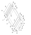
- FIG. 1 is a perspective view of a cassette type detector.
- a cassette type detector 1 which is a radiation image detection cassette is a cassette type flat panel detector.
- the cassette type detector 1 includes a radiation detection unit 2 (see FIG. 3 and the like) that detects irradiated radiation and acquires it as digital image data, and a housing (housing) 3 that houses the radiation detection unit 2 therein. I have.
- the housing 3 is formed so that the thickness in the radiation incident direction is 15 mm.
- the thickness of the housing 3 in the radiation incident direction is preferably 16 mm or less, and has a size (15 mm + 1 mm and 15 mm-2 mm) in accordance with the standard (JIS Z 4905) standard for screen / film cassettes. It is preferable to be within the range (the international standard corresponding to JIS Z 4905 is IEC 60406).
- FIG. 2 is an exploded perspective view of the housing 3.
- the housing 3 includes a hollow main body 31 having openings 311 and 312 at both ends, a first lid member 32 and a second lid 32 that close the openings 311 and 312 of the main body 31. And a lid member 33.
- the main body 31 is made of a carbon fiber body (for example, carbon fiber reinforced plastic: CFRP), and is lightweight and excellent in strength.
- CFRP carbon fiber reinforced plastic
- the thickness of the main body 31 is cylindrical so that the strength of the cassette type detector 1 is maintained.
- the first lid member 32 and the second lid member 33 include lid body portions 321 and 331 and insertion portions 322 and 332, and are formed of aluminum.
- Engagement pieces 324 and 334 that engage the first lid member 32 and the second lid member 33 and the main body 31 are inserted into the openings 311 and 312 on the side surfaces of the insertion portions 322 and 332, respectively. Extends in the direction. Engagement projections 325 and 335 are provided on the outer surfaces of the engagement pieces 324 and 334, respectively. When the first lid member 32 and the second lid member 33 are inserted into the main body portion 31, the engagement convex portions 325 and 335 engage with the engagement concave portions 315 and 316 installed in the main body portion 31.
- a wireless communication unit 4 for wirelessly transmitting and receiving information between the cassette type detector 1 and an external device is embedded in one side surface of the lid main body 321 in the first lid member 32, and wirelessly
- the communication unit 4 is provided with a pair of flat radiation plates 41 and 42 made of metal and a power feeding unit 43 that supplies power to the pair of radiation plates 41 and 42.
- the rechargeable battery 24 (see FIG. 3 and the like) provided inside the housing 3 on one surface of the lid main body 321 on the same surface as the surface on which the wireless communication unit 4 is formed.
- a charging terminal 51 connected to an external power source and the like, and a power switch 52 for switching ON / OFF of the power source of the cassette type detector 1 are provided.
- the corner formed by the surface on which the wireless communication unit 4 is formed and the surface on the radiation incident side is composed of, for example, an LED or the like and displays an indicator for charging the rechargeable battery 24 and various operation states. 53 is provided.
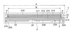
- FIG. 3 is a cross-sectional view of a predetermined portion of the cassette type detector 1 shown in FIG.
- the radiation detection unit 2 includes a detector unit 21, a base 22, and electrical components (a relay board 23A, a control board 23B, a rechargeable battery 24 (for example, a lithium-in capacitor)).
- the detector unit 21 is supported on the upper surface of the base 22, and a plurality of electrical components such as the control board 23 ⁇ / b> B and the rechargeable battery 24 are attached to the lower surface of the base 22. Yes.
- the base 22 is flexible and made of resin.
- the material of the base 22 is, for example, a resin in which polycarbonate and ABS are mixed.
- the base 22 supports the glass substrate 213, and although not shown in FIG. 3, a thin lead layer is interposed between the base 22 and the glass substrate 213.
- the detector unit 21 includes a scintillator 211, a detector 212, a glass substrate 213, a counter substrate 214, and the like.
- a detector 212 is installed on a glass substrate 213, and a scintillator 211 is installed above the detector 212.
- a counter substrate 214 is installed above the scintillator 211, and the scintillator 211 is sandwiched between the counter substrate 214 and the glass substrate 213.
- the glass substrate 213 and the counter substrate 214 are both substrates having a thickness of about 0.6 mm, for example.
- the scintillator 211 has a function of converting incident radiation into light.
- the scintillator 211 has, for example, a phosphor as a main component, and outputs an electromagnetic wave having a wavelength of 300 nm to 800 nm, that is, an electromagnetic wave (light) ranging from ultraviolet light to infrared light centering on visible light, based on incident radiation. It has become.
- the detection unit 212 converts the electromagnetic wave (light) output from the scintillator 211 into electric energy and accumulates it, and outputs an electric signal based on the accumulated electric energy.
- the electrical signal generated by the detection unit 212 is sent to the first relay board 23A by a flexible harness (not shown).
- a buffer member 215 is installed between the end of the base 22 and the inner side P of the housing 3 or above the counter substrate 214.
- the cassette type detector 1 shown in FIGS. 1 to 3 conforms to the standard (JIS) size of a conventional cassette for screens / films so that it can be used for existing equipment (Bucky etc.). It has become.
- “A” shown in FIG. 3 is the outer length of the housing 3, and “B” is the same direction as the outer length A (the same direction means the same direction as the direction in which the outer length A of the housing 3 is measured).
- the B / A value of the cassette type detector 1 in this embodiment is 0.95
- the B / A value of the standard type cassette type detector is in the range of 0.85 to 0.95.
- the radiation detection area occupies a large proportion with respect to the outer shape of the housing 3, the end of the detection unit 212 and the glass substrate 213, and the inner side P of the housing 3 (see FIG. 3). There is almost no space between. Accordingly, it is not possible to sufficiently install the buffer member 215 between the end of the detection unit 212 or the glass substrate 213 and the inner side P of the housing 3.
- a side wall 22A is provided at the end of the base 22. Since the side wall 22A is provided as shown in FIG. 3, the contact area between the base 22 and the buffer member 215 can be increased. Therefore, even if the buffer member 215 is thin, the side of the housing 3 (left and right in FIG. 3) The sudden impact applied to the base 22 from the direction) is mitigated, and the glass substrate 213 and the like can be prevented from being damaged. Further, even if the side wall 22A is provided at the end of the base 22, the area where the control board 23B is installed in the base 22 does not become thick as shown in FIG. You can also plan.
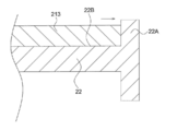
- FIG. 4 is an enlarged view of the X region in FIG. A side wall 22 ⁇ / b> A of the base 22 is provided at the end of the glass substrate 213.
- a double-sided tape 22B described later is installed, but the double-sided tape 22B is not installed, and the side of the housing 3 with the glass substrate 213 simply placed without being fixed to the base 22 is provided. If a sudden impact is applied from the side, even if the impact applied to the base 22 is mitigated by the side wall 22A or the buffer member, the glass substrate 213 is displaced in the direction of the arrow in FIG. There is a possibility that the end portion of the glass substrate 213 may be damaged by colliding with the side wall 22A of the glass substrate 213.
- the glass substrate 213 according to this embodiment is supported in a state of being bonded to the base 22.
- a double-sided tape 22B (thickness of about 0.1 to 0.2 mm) indicated by a broken line is installed between the glass substrate 213 and the base 22, and the glass substrate 213 and the base 22 are double-sided. Bonded with tape 22B.
- any form may be employed as long as the glass substrate 213 is supported in a state of being bonded to the base 22 (may be bonded by an adhesive instead of a double-sided tape).
- the case where the glass substrate 213 is not fixed to the base 22 and is simply placed is compared with the case where the glass substrate 213 is supported while being bonded to the base 22, and the cassette type Through experiments, it was confirmed at what rate the breakage of the glass substrate 213 occurs when a sudden impact is applied to the detector 1.
- the cassette-type detector 1 is dropped a plurality of times from a predetermined height H (the height at which the cassette-type detector 1 may be dropped when it is actually carried), and the glass substrate The rate at which 213 breaks was confirmed.
- the glass substrate 213 When the glass substrate 213 was not placed on the base 22 and was simply placed, the glass substrate 213 was broken three times out of six times when dropped from a height H of 60 cm. When dropped from a height H of 75 cm, the glass substrate 213 was broken four times in six times, and when dropped from a height H of 90 cm, the glass substrate 213 was broken six times in six times. On the other hand, when the glass substrate 213 was supported while being bonded to the base 22, the glass substrate 213 was not damaged at all when dropped from any height.
- the present invention is effective in a standard size cassette type detector having little space for installing a buffer member.
- FIG. 6 shows another embodiment.
- the end of the glass substrate 213 is in contact with the side wall 22A of the base 22, and no gap is provided between the end of the glass substrate 213 and the side wall 22A of the base 22.
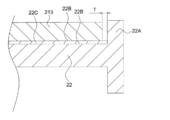
- a gap T (about 1 mm) is provided between the end of the glass substrate 213 and the side wall 22 ⁇ / b> A of the base 22.
- the glass substrate 213 and the base 22 shown in FIG. 6 are bonded with a double-sided tape 22B as in the embodiment of FIG.
- the glass substrate 213 and the base 22 are bonded even if there is no gap between the end of the glass substrate 213 and the side wall 22A of the base 22 as in the embodiment shown in FIG. Since the end portion of the glass substrate 213 is not displaced and collides with the side wall 22A of the base 22, the glass substrate 213 is not damaged by a sudden impact. However, if the glass substrate 213 and the base 22 are bonded as shown in FIG. 6 and a gap T is provided between the end of the glass substrate 213 and the side wall 22A of the base 22, a considerably strong impact is generated.
- the end portion of the glass substrate 213 and the side wall 22A of the base 22 do not collide, and the glass substrate 213 is not damaged. That is, by providing the gap T between the end of the glass substrate 213 and the side wall 22A of the base 22, it is possible to prevent the glass substrate 213 from being damaged even against a considerably strong impact, which is more effective. .
- FIG. 7 shows still another embodiment.
- the buffer member 22 ⁇ / b> C for dispersing the load applied when the patient lies on the cassette-type detector 1 at the time of detecting the radiographic image is provided between the glass substrate 213 and the base 22.
- the buffer member 22C is made of foamed polyethylene or the like and has a thickness of about 0.5 to 1.0 mm.
- the buffer member 22C and the glass substrate 213 are bonded by a double-sided tape 22B, and the buffer member 22C and the base 22 are also bonded by a double-sided tape 22B.
- the buffer member 22C When the buffer member 22C is disposed, the load applied to the glass substrate 213 and the like is dispersed. However, when a sudden impact is applied from the side of the cassette type detector 1, the glass substrate 213 is easily displaced from the base 22. Therefore, by disposing the buffer member 22C and providing a gap T between the end of the glass substrate 213 and the side wall 22A of the base 22 in the same manner as in FIG. 6, dispersion of the load applied to the glass substrate 213 and the glass substrate It is possible to achieve both prevention of damage of 213.
- the cassette type detector 1 may be accidentally dropped or collided with another object while the cassette type detector 1 is being transported to a predetermined place. Sudden impact may be applied to. After an impact is applied to the cassette type detector 1, the user may not be able to determine whether or not the cassette type detector 1 can operate normally. For example, even if a part of the detection unit 212 is damaged by an impact, a radiographic image detection operation is possible as long as the detection unit 212 does not have an electrical failure. Will continue to perform detection without recognizing a failure.
- the manufacturer specifies the cumulative number of impacts applied to the cassette type detector 1 (for example, the number of drops) from the viewpoint of durability, how many times the impact is applied to the cassette type detector 1.
- the cumulative number of impacts applied to the cassette type detector 1 for example, the number of drops
- the cassette type detector 1 is provided with means for detecting an impact, and it is determined whether or not the cassette type detector 1 has failed based on the degree of impact detected by the means and the cumulative number of impacts.
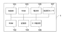
- FIG. 8 is a block diagram showing a configuration related to an operation for detecting a shock applied to the cassette type detector 1 and recognizing a failure.
- the control unit 101 is composed of, for example, a CPU, reads out a control program stored in the ROM 102, develops it in a work area formed in the RAM 103, and controls each part of the cassette type detector 1 according to the control program. .
- the ROM 102 is configured by a non-volatile semiconductor memory or the like, and stores a control program executed by the control unit 101, various programs, and the like.
- the RAM 103 forms a work area that temporarily stores various programs, input or output data, parameters, and the like that can be executed by the control unit 101 read from the ROM 102 in various processes that are executed and controlled by the control unit 101. .
- the storage unit 104 is composed of, for example, a nonvolatile memory such as a flash memory or a RAM, and stores the cumulative number of impacts detected by the acceleration sensor 107.
- the power supply unit 105 supplies power to the control unit 101, the acceleration sensor 107, and the like. Normally, power is supplied to each unit by the power supply unit 105. When the power supply unit 105 is turned off, the sub power supply unit 106 supplies power to the control unit 101, the acceleration sensor 107, and the like.
- the acceleration sensor 107 is, for example, a two-axis type that detects acceleration in the X-axis direction and the Y-axis direction, or a three-axis type that detects acceleration in the X-axis direction, the Y-axis direction, and the Z-axis direction. Based on the waveform of the output signal from the acceleration sensor 107, it is possible to detect that an impact has been applied to the cassette type detector 1. Specifically, the peak value of the waveform of the output signal in the acceleration sensor 107 is low unless an impact is applied to the cassette type detector 1, but the peak value of the waveform increases when an impact is applied to the cassette type detector 1. By detecting this change in peak value, it is possible to detect that an impact has been applied to the cassette type detector 1.
- the number of times when the peak value of the waveform is greater than or equal to the reference value is counted, and the number of times is stored in the storage unit 104.
- the installation position of the acceleration sensor 107 in the cassette type detector 1 is near the center of the cassette type detector 1.
- the power supply unit 105 of the cassette type detector 1 When the power supply unit 105 of the cassette type detector 1 is turned on, the cumulative number of impacts (history information) stored in the storage unit 104 is checked. If the cumulative number is less than the reference number, the power supply unit 105 is turned on as it is. If the cumulative number is equal to or greater than the reference number, the cassette-type detector 1 has a high probability of failure. A warning is displayed on a device that is communicating through the communication unit 4, and the power supply unit 105 is turned off.
- the power supply unit 105 of the cassette type detector 1 When the power supply unit 105 of the cassette type detector 1 is ON, the waveform of the output signal from the acceleration sensor 107 is monitored. If it is determined that the peak value of the waveform is greater than or equal to the first reference value, it is determined that a considerably large impact has been applied to the cassette type detector 1, and the probability that the cassette type detector 1 has failed is high, so the indicator 53 is warned.
- the power supply unit 105 is turned off by displaying a color or displaying a warning on a device communicating via the wireless communication unit 4.
- the cassette type detector 1 performs self-analysis, and if a failure is found somewhere, a warning color is similarly displayed on the indicator 53. Or a warning is displayed on a device communicating via the wireless communication unit 4 to turn off the power supply unit 105. If no failure is found, the power supply unit 105 is turned on as it is.
- the cumulative number of impacts applied to the cassette type detector 1 is increased by 1 and the cumulative number Is less than the reference number of times, the probability that the cassette type detector 1 has failed is low, so the power supply unit 105 is turned on as it is, and if it is greater than the reference number, the probability that the cassette type detector 1 has failed is high.
- a warning color is displayed on 53, or a warning is displayed on a device communicating via the wireless communication unit 4, so that the power supply unit 105 is turned off.
- the cassette type detector 1 is provided with means for detecting an impact, and it is determined whether or not the cassette type detector 1 has failed based on the degree of impact detected by the means and the cumulative number of impacts, It is possible to prevent the user from informing the user that a failure has occurred and to prevent unnecessary radiation image detection operations from being executed.
Landscapes
- Physics & Mathematics (AREA)
- General Physics & Mathematics (AREA)
- Apparatus For Radiation Diagnosis (AREA)
- Radiography Using Non-Light Waves (AREA)
- Measurement Of Radiation (AREA)
Abstract
Description
被写体に向けて照射された放射線を検出して放射線画像データを取得する可搬型の放射線画像検出カセッテであって、
入射した放射線に対応した電気信号を出力する検出部と、
当該検出部が設置されたガラス基板と、
前記ガラス基板を支持する基台と、
少なくとも前記検出部、前記ガラス基板、及び前記基台を内蔵する筐体と、
前記基台の端部と前記筐体の内側との間に設けられた緩衝部材と、を有し、
前記基台の端部には側壁が設けられており、
前記ガラス基板は前記基台に対して接着された状態で支持されていることを特徴とするものである。
図1は、カセッテ型検出器の斜視図である。放射線画像検出カセッテであるカセッテ型検出器1は、カセッテ型のフラットパネルディテクタ(Flat Panel Detector)である。カセッテ型検出器1は、照射された放射線を検出してデジタル画像データとして取得する放射線検出部2(図3等参照)と、放射線検出部2を内部に収納するハウジング(筐体)3とを備えている。
次にカセッテ型検出器1の内部構造について説明する。図3は、図1に示すカセッテ型検出器1をa方向から見た所定箇所の断面図である。
次にガラス基板213の破損防止に関する構造について説明する。
前述したように、カセッテ型検出器1を所定の場所に運ぶ最中に誤ってカセッテ型検出器1を落下させてしまったり、他の物体に衝突させてしまったりして、カセッテ型検出器1に突発的な衝撃が加わる場合がある。カセッテ型検出器1に衝撃が加わった後、カセッテ型検出器1が正常に動作可能か否かをユーザーが判断出来ない場合がある。例えば、検出部212の一部が衝撃により損傷したとしても電気的に故障していなければ放射線画像の検出動作が可能であり、検出部212の一部が正常に動作しないにもかかわらず、ユーザーは故障を認識せずに検出動作を継続して実行してしまう。
2 放射線検出部
3 ハウジング
21 検出器ユニット
22 基台
22A 側壁
22B 両面テープ
22C 緩衝部材
211 シンチレータ
212 検出部
213 ガラス基板
214 対向基板
Claims (4)
- 被写体に向けて照射された放射線を検出して放射線画像データを取得する可搬型の放射線画像検出カセッテであって、
入射した放射線に対応した電気信号を出力する検出部と、
当該検出部が設置されたガラス基板と、
前記ガラス基板を支持する基台と、
少なくとも前記検出部、前記ガラス基板、及び前記基台を内蔵する筐体と、
前記基台の端部と前記筐体の内側との間に設けられた緩衝部材と、を有し、
前記基台の端部には側壁が設けられており、
前記ガラス基板は前記基台に対して接着された状態で支持されていることを特徴とする放射線画像検出カセッテ。 - 前記ガラス基板の端部と前記側壁の間に隙間が設けられている請求項1に記載の放射線画像検出カセッテ。
- 前記ガラス基板と前記基台との間に緩衝部材が配置されている請求項2に記載の放射線画像検出カセッテ。
- 前記筐体の外形長さをA、当該外形長さと同方向における放射線画像検出カセッテの検出領域長さをBとした場合、B/Aの値が0.85から0.95の範囲内である請求項1~3のいずれかに記載の放射線画像検出カセッテ。
Priority Applications (2)
| Application Number | Priority Date | Filing Date | Title |
|---|---|---|---|
| US13/262,045 US20120018633A1 (en) | 2009-04-10 | 2010-02-05 | Radiation image detecting cassette |
| JP2011508268A JPWO2010116784A1 (ja) | 2009-04-10 | 2010-02-05 | 放射線画像検出カセッテ |
Applications Claiming Priority (2)
| Application Number | Priority Date | Filing Date | Title |
|---|---|---|---|
| JP2009-095698 | 2009-04-10 | ||
| JP2009095698 | 2009-04-10 |
Publications (1)
| Publication Number | Publication Date |
|---|---|
| WO2010116784A1 true WO2010116784A1 (ja) | 2010-10-14 |
Family
ID=42936073
Family Applications (1)
| Application Number | Title | Priority Date | Filing Date |
|---|---|---|---|
| PCT/JP2010/051689 Ceased WO2010116784A1 (ja) | 2009-04-10 | 2010-02-05 | 放射線画像検出カセッテ |
Country Status (3)
| Country | Link |
|---|---|
| US (1) | US20120018633A1 (ja) |
| JP (1) | JPWO2010116784A1 (ja) |
| WO (1) | WO2010116784A1 (ja) |
Cited By (2)
| Publication number | Priority date | Publication date | Assignee | Title |
|---|---|---|---|---|
| JP2016001128A (ja) * | 2014-06-11 | 2016-01-07 | キヤノン株式会社 | 放射線画像撮像装置及びその制御方法、並びに、プログラム |
| JP2022008628A (ja) * | 2016-12-02 | 2022-01-13 | コニカミノルタ株式会社 | 放射線画像撮影装置及び放射線画像撮影システム |
Families Citing this family (2)
| Publication number | Priority date | Publication date | Assignee | Title |
|---|---|---|---|---|
| JP2014235145A (ja) * | 2013-06-05 | 2014-12-15 | セイコーエプソン株式会社 | テラヘルツ波検出装置、カメラ、イメージング装置および計測装置 |
| JP7181050B2 (ja) * | 2018-10-18 | 2022-11-30 | 浜松ホトニクス株式会社 | 放射線撮像装置 |
Citations (4)
| Publication number | Priority date | Publication date | Assignee | Title |
|---|---|---|---|---|
| JP2002014168A (ja) * | 2000-06-27 | 2002-01-18 | Canon Inc | X線撮像装置 |
| JP2004219705A (ja) * | 2003-01-15 | 2004-08-05 | Konica Minolta Holdings Inc | 放射線画像撮影用カセッテ |
| JP2006521130A (ja) * | 2003-03-24 | 2006-09-21 | カルテンバッハ ウント ホイクト ゲゼルシャフト ミット ベシュレンクテル ハフツング ウント カンパニー カーゲー | 口腔内センサ |
| JP2009020099A (ja) * | 2007-07-10 | 2009-01-29 | General Electric Co <Ge> | ディジタルx線検出器 |
Family Cites Families (3)
| Publication number | Priority date | Publication date | Assignee | Title |
|---|---|---|---|---|
| US7514703B2 (en) * | 2003-06-10 | 2009-04-07 | Fujifilm Corporation | Image information detecting cassette |
| JP2005000370A (ja) * | 2003-06-11 | 2005-01-06 | Canon Inc | X線撮影装置 |
| US20090090850A1 (en) * | 2006-08-31 | 2009-04-09 | Aptina Imaging Corporation | Deep Recess Color Filter Array and Process of Forming the Same |
-
2010
- 2010-02-05 JP JP2011508268A patent/JPWO2010116784A1/ja active Pending
- 2010-02-05 US US13/262,045 patent/US20120018633A1/en not_active Abandoned
- 2010-02-05 WO PCT/JP2010/051689 patent/WO2010116784A1/ja not_active Ceased
Patent Citations (4)
| Publication number | Priority date | Publication date | Assignee | Title |
|---|---|---|---|---|
| JP2002014168A (ja) * | 2000-06-27 | 2002-01-18 | Canon Inc | X線撮像装置 |
| JP2004219705A (ja) * | 2003-01-15 | 2004-08-05 | Konica Minolta Holdings Inc | 放射線画像撮影用カセッテ |
| JP2006521130A (ja) * | 2003-03-24 | 2006-09-21 | カルテンバッハ ウント ホイクト ゲゼルシャフト ミット ベシュレンクテル ハフツング ウント カンパニー カーゲー | 口腔内センサ |
| JP2009020099A (ja) * | 2007-07-10 | 2009-01-29 | General Electric Co <Ge> | ディジタルx線検出器 |
Cited By (3)
| Publication number | Priority date | Publication date | Assignee | Title |
|---|---|---|---|---|
| JP2016001128A (ja) * | 2014-06-11 | 2016-01-07 | キヤノン株式会社 | 放射線画像撮像装置及びその制御方法、並びに、プログラム |
| JP2022008628A (ja) * | 2016-12-02 | 2022-01-13 | コニカミノルタ株式会社 | 放射線画像撮影装置及び放射線画像撮影システム |
| JP7207482B2 (ja) | 2016-12-02 | 2023-01-18 | コニカミノルタ株式会社 | 放射線画像撮影装置及び放射線画像撮影システム |
Also Published As
| Publication number | Publication date |
|---|---|
| US20120018633A1 (en) | 2012-01-26 |
| JPWO2010116784A1 (ja) | 2012-10-18 |
Similar Documents
| Publication | Publication Date | Title |
|---|---|---|
| CN110196447B (zh) | 放射线检测装置 | |
| US20120068073A1 (en) | Cassette type radiographic image solid-state detector | |
| CN110960236B (zh) | 放射线检测装置 | |
| WO2010116784A1 (ja) | 放射線画像検出カセッテ | |
| JP5692077B2 (ja) | 放射線画像検出カセッテ | |
| CN111317488A (zh) | 放射线摄影装置 | |
| JP5381327B2 (ja) | 放射線画像検出カセッテ | |
| CN113053677B (zh) | 电源单元和包括电源单元的放射线摄像装置 | |
| JP2009257914A (ja) | カセッテ型放射線画像検出器 | |
| CN102549455B (zh) | 放射线图像检测盒 | |
| US11099286B2 (en) | Radiation detection device | |
| JP2010127882A (ja) | 放射線画像検出装置 | |
| JP2010127680A (ja) | 放射線画像検出センサユニット | |
| JP7810011B2 (ja) | 放射線撮影装置 | |
| JP2025137662A (ja) | 放射線撮影装置 | |
| JP2011090024A (ja) | 放射線画像検出カセッテ | |
| JP2023124928A (ja) | 放射線撮影装置 | |
| CN110960237B (zh) | 放射线检测装置 | |
| JP2011045213A (ja) | カセッテ充電装置 | |
| JP2010217498A (ja) | 放射線画像検出カセッテ | |
| US20230125648A1 (en) | Radiographing apparatus | |
| US12602763B2 (en) | Radiographic imaging apparatus and maintenance management system | |
| JP2010249722A (ja) | 放射線画像検出カセッテ | |
| US20240402365A1 (en) | Radiation imaging apparatus | |
| JP2024076513A (ja) | 放射線画像撮影装置 |
Legal Events
| Date | Code | Title | Description |
|---|---|---|---|
| 121 | Ep: the epo has been informed by wipo that ep was designated in this application |
Ref document number: 10761486 Country of ref document: EP Kind code of ref document: A1 |
|
| WWE | Wipo information: entry into national phase |
Ref document number: 2011508268 Country of ref document: JP |
|
| WWE | Wipo information: entry into national phase |
Ref document number: 13262045 Country of ref document: US |
|
| NENP | Non-entry into the national phase |
Ref country code: DE |
|
| 122 | Ep: pct application non-entry in european phase |
Ref document number: 10761486 Country of ref document: EP Kind code of ref document: A1 |