WO2010116428A1 - 試料作製装置、及び試料作製装置における制御方法 - Google Patents
試料作製装置、及び試料作製装置における制御方法 Download PDFInfo
- Publication number
- WO2010116428A1 WO2010116428A1 PCT/JP2009/005580 JP2009005580W WO2010116428A1 WO 2010116428 A1 WO2010116428 A1 WO 2010116428A1 JP 2009005580 W JP2009005580 W JP 2009005580W WO 2010116428 A1 WO2010116428 A1 WO 2010116428A1
- Authority
- WO
- WIPO (PCT)
- Prior art keywords
- sample
- ion beam
- transfer means
- extracted
- probe
- Prior art date
- Legal status (The legal status is an assumption and is not a legal conclusion. Google has not performed a legal analysis and makes no representation as to the accuracy of the status listed.)
- Ceased
Links
Images


Classifications
-
- G—PHYSICS
- G01—MEASURING; TESTING
- G01N—INVESTIGATING OR ANALYSING MATERIALS BY DETERMINING THEIR CHEMICAL OR PHYSICAL PROPERTIES
- G01N1/00—Sampling; Preparing specimens for investigation
- G01N1/28—Preparing specimens for investigation including physical details of (bio-)chemical methods covered elsewhere, e.g. G01N33/50, C12Q
- G01N1/286—Preparing specimens for investigation including physical details of (bio-)chemical methods covered elsewhere, e.g. G01N33/50, C12Q involving mechanical work, e.g. chopping, disintegrating, compacting, homogenising
Definitions
- the present invention relates to a method for extracting a minute region of a sample with a focused ion beam.
- Patent Document 1 a part of a sample substrate is processed into a cantilever type by sputtering of a focused ion beam, a probe is brought into contact with a part of the extracted sample, and adhered by a FIB-induced deposition film. Sputtering is performed on the connection between the sample and the sample substrate, and the extracted sample is separated from the sample substrate.
- Patent Document 2 Japanese Patent No. 3547143 (Patent Document 2) and Japanese Patent No. 3695181 (Patent Document 3), a micro sample extracted by a focused ion beam is transferred to a sample holder arranged in a sample chamber, and the sample holder And a micro sample are adhered by a FIB-induced deposition film. Further, it is disclosed that a mark for specifying a region to be observed is provided on a sample substrate before extracting a micro sample with a focused ion beam.
- the inventor of the present application diligently studied the automation of a method of extracting a minute region of a sample with a focused ion beam, and the following knowledge was obtained.
- Patent Documents 1 to 3 a specific method for the focused ion beam apparatus to automatically perform the process of performing sputtering processing on the connection between the extracted sample and the sample substrate and separating the extracted sample from the sample substrate is described. It has not been. In addition, when the process is performed through human judgment, it is difficult to improve the yield beyond a certain fixed line.
- the adhesive part that is not completely separated may be peeled off and the sample substrate may fall off. There is also.
- An object of the present invention relates to automatically separating an extracted sample from a sample.
- the present invention provides an index for improving the accuracy of image recognition in a region to be an extracted sample in a sample, a region other than that, or a transfer means for transferring the extracted sample, or a sample holder that can hold the extracted sample.
- the present invention relates to image recognition of a sample and the relative movement of the sample with high accuracy.
- the present invention in the sampling of a micro sample using a focused ion beam, it becomes possible to automatically detect the end point of separation processing between the sample and the sample. For this reason, for example, unmanned sample extraction can be performed, and a large amount of sample preparation can be performed.
- substrate and the mark on a sample extraction part Observation image from the upper surface when the probe is in contact with the inner wall of the peripheral hole. An observation image from the upper surface when the probe is brought into contact with the sample extraction part. An observation image from the upper surface before probe bonding. Observation image when the probe is bonded to the sample extraction part and the bottom cutout pattern is placed. An observation image from above when the sample is extracted. Sectional drawing at the time of bottom cutting. Sectional drawing when the adhesion
- step difference probe with a mark is moved on the surrounding processing hole on the extraction point.
- Sectional drawing when the step probe with a mark contacts the substrate.
- Sectional drawing when a stage is moved and the stepped probe tip with a mark is made to contact an extraction part.
- the top view when a stage is moved and the step probe with a mark is made to contact an extraction part.
- the figure which shows the positional relationship of a sample, a probe, and a gas nozzle when forming a probe adhesion deposit film An observation image when a probe adhesion deposit film is formed and a bottom cut pattern is arranged. Observation image when the end of bottom cutting is detected. Observation image when the sample carrier is moved near the sample and the probe.
- Sectional drawing which shows the positional relationship of an extraction sample, a probe, and a sample carrier Sectional drawing which shows the positional relationship at the time of adhere
- An intermediate shape for thinning the sample on the sample carrier The top view when a rotating probe and a sample extraction part are made to contact. Sectional drawing when a rotating probe and a sample extraction part are made to contact. Sectional drawing when rotating a rotating probe and making it contact the sample upper part.
- a sample stage on which a sample can be placed, an ion beam optical system capable of irradiating an ion beam, a transfer means capable of transporting an excised sample separated from the sample by ion beam irradiation, and the ion beam optical system are controlled.
- a mark that is formed in a region that becomes the extracted sample in the sample when the sample is irradiated with an ion beam to separate the extracted sample from the sample, and other regions A sample preparation apparatus is disclosed that is configured to measure marks formed on the surface and stop ion beam irradiation when the relative position between the marks reaches a predetermined condition.
- a sample stage on which a sample can be placed an ion beam optical system capable of irradiating an ion beam, a transfer means capable of transporting an extracted sample separated from the sample by ion beam irradiation, and the ion beam optical system
- an arithmetic device that can control the sample, and is formed in a transfer means for holding a region to be the extracted sample in the sample when the sample is irradiated with an ion beam to separate the extracted sample from the sample.
- the mark and a mark formed in a region other than the region to be the extracted sample in the sample are measured, and the ion beam irradiation is stopped when a relative position between the marks becomes a predetermined condition.
- a sample preparation apparatus is disclosed.
- a sample stage on which a sample can be placed an ion beam optical system capable of irradiating an ion beam, a transfer means capable of transporting an extracted sample separated from the sample by ion beam irradiation, and the ion beam optical system
- An arithmetic unit capable of controlling the movement, and when moving the transfer means to bring the transfer means into contact with the extracted sample, a mark formed on the transfer means and a region to be the extracted sample in the sample
- a sample preparation apparatus is disclosed that is configured to measure the marks formed in the above and stop the transfer means when the relative position between the marks reaches a predetermined condition.
- a sample stage on which a sample can be placed an ion beam optical system capable of irradiating an ion beam, a transfer means capable of transporting an extracted sample separated from the sample by ion beam irradiation, and the ion beam optical system
- An arithmetic unit capable of controlling the movement, and when moving the transfer means to bring the transfer means into contact with the extracted sample, a mark formed on the transfer means and a region to be the extracted sample in the sample.
- a sample preparation apparatus configured to measure marks formed in a region other than the above and stop the transfer means when the relative position between the marks reaches a predetermined condition.
- a sample stage on which a sample can be placed an ion beam optical system capable of irradiating an ion beam, a transfer means capable of transporting an extracted sample separated from the sample by ion beam irradiation, and holding the extracted sample A mark holder formed on the extracted sample when the extracted sample held by the transfer means is transferred to the sample holder.
- a sample preparation device configured to measure the marks formed on the sample holder and stop the movement of the transfer means when the relative position between the marks reaches a predetermined condition.
- a sample stage on which a sample can be placed an ion beam optical system capable of irradiating an ion beam, a transfer means capable of transporting an extracted sample separated from the sample by ion beam irradiation, and holding the extracted sample
- a sample holder capable of controlling the ion beam optical system, and the transfer means for transferring the extracted sample when the extracted sample held by the transfer means is transferred to the sample holder.
- the sample is configured to measure the mark formed on the sample holder and the mark formed on the sample holder, and stop the movement of the transfer means when the relative position between the marks reaches a predetermined condition.
- a sample stage on which a sample can be placed an ion beam optical system capable of irradiating an ion beam, a transfer means capable of transporting an extracted sample separated from the sample by ion beam irradiation, and the ion beam optical system
- a control method in a sample preparation apparatus comprising: an arithmetic device capable of controlling the region, wherein when the sample is irradiated with an ion beam and the sample is separated from the sample, the sample becomes a region to be the sample to be extracted
- a method is disclosed in which the marks formed in the above and the marks formed in other regions are measured, and the ion beam irradiation is stopped when the relative position between the marks reaches a predetermined condition.
- a control method in a sample preparation apparatus comprising: an arithmetic device capable of controlling the region, wherein when the sample is irradiated with an ion beam and the sample is separated from the sample, the sample becomes a region to be the sample to be extracted When the mark formed on the transfer means for holding the mark and the mark formed in a region other than the region to be the extracted sample in the sample are measured, and the relative position between the marks becomes a predetermined condition, A method for stopping beam irradiation is disclosed.
- a sample stage on which a sample can be placed an ion beam optical system capable of irradiating an ion beam, a transfer means capable of transporting an extracted sample separated from the sample by ion beam irradiation, and the ion beam optical system
- a control method in a sample preparation apparatus comprising: a mark formed on the transfer means when the transfer means is moved to bring the transfer means into contact with the extracted sample;
- a method is disclosed in which a mark formed in a region to be the extracted sample in the sample is measured, and the transfer means is stopped when a relative position between the marks becomes a predetermined condition.
- a sample stage on which a sample can be placed, an ion beam optical system capable of irradiating an ion beam, a transfer means capable of transporting an extracted sample separated from the sample by ion beam irradiation, and the ion beam optical system A control method in a sample preparation apparatus comprising: a mark formed on the transfer means when the transfer means is moved to bring the transfer means into contact with the extracted sample; A method of measuring a mark formed in a region other than the region to be the extracted sample in the sample and stopping the transfer means when the relative position between the marks becomes a predetermined condition is disclosed.
- a sample stage on which a sample can be placed an ion beam optical system capable of irradiating an ion beam, a transfer means capable of transporting an extracted sample separated from the sample by ion beam irradiation, and holding the extracted sample A sample holder, and an arithmetic device capable of controlling the ion beam optical system, the method for controlling the sample preparation apparatus, wherein the extracted sample held in the transfer means is transferred to the sample holder.
- a sample stage on which a sample can be placed an ion beam optical system capable of irradiating an ion beam, a transfer means capable of transporting an extracted sample separated from the sample by ion beam irradiation, and holding the extracted sample A sample holder, and an arithmetic device capable of controlling the ion beam optical system, the method for controlling the sample preparation apparatus, wherein the extracted sample held in the transfer means is transferred to the sample holder.
- a method of stopping is disclosed.
- the sample preparation apparatus includes an electron beam column that can irradiate an electron beam, and the mark is measured by the electron beam.
- condition of the ion beam when measuring the mark can be changed from the condition of the ion beam when processing the sample.
- the ion beam is a focused ion beam. It is also disclosed that the ion beam is a projection ion beam.
- the transfer means includes a probe. Further, it is disclosed that a step is provided in a region to be contacted with the extracted sample in the probe. Further, it is disclosed that the probe has two or more steps arranged in the probe axial direction at the tip. Further, it is disclosed that the probe has at least two or more steps arranged in a substantially vertical direction of the probe axis at the tip.
- the transfer means includes a micromanipulator.
- the embodiment discloses that the sample stage and / or the transfer means are micro-driven so that a pressure is generated between the extracted sample and the transfer means.
- the probe is rotated around the probe axis so that a pressure is generated between the extracted sample and the probe.
- the mark is formed in the region that becomes the extracted sample in the sample and / or the region other than the region that becomes the extracted sample in the sample. To create a mark, which is.
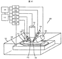
- FIG. 41 is a schematic diagram of the charged particle beam apparatus in the present embodiment, which is drawn by seeing through a part of the inside of the apparatus.
- the charged particle beam apparatus 100 includes a focused ion beam column 101 that generates an ion beam for observing and processing a sample and a probe, an electron beam column 102 that generates an electron beam for observing the surface shape of the sample and the probe, and a vacuum sample chamber. 103, a sample stage 104 on which a sample is placed, a probe driving unit 106 for finely moving the probe 105 in the vacuum sample chamber 103, a detector 108, a deposition gas source 115, a display 109, and a calculation processing unit 110.
- the focused ion beam column 101 observes or processes the surface of the sample 111 or the probe 105 by irradiating the sample 111 or the probe 105 with a beam of ions generated from an ion source (not shown). be able to.
- the electron beam column 102 can observe the surface of the sample 111 or the probe 105 by irradiating the sample 111 or the probe 105 with electrons generated from an electron source (not shown) in the form of a beam.
- the focused ion beam column 101 is arranged in the vertical direction, and the electron beam column 102 is arranged in a direction inclined with respect to the horizontal plane.
- the arrangement is not limited to this, and for example, the electron beam column 102 may be arranged in the vertical direction, and the focused ion beam column 101 may be arranged in a direction inclined with respect to the horizontal plane.
- a projection ion beam apparatus may be used instead of the focused ion beam.
- a single column focused ion beam device that does not include an electron beam column or a triple column device that further includes a gaseous ion beam column such as argon may be used.
- the sample stage 104 can place the sample 111, and a position necessary for ion beam processing and observation can be moved to an ion beam irradiation position or moved to an observation position by an electron beam.
- a position necessary for ion beam processing and observation can be moved to an ion beam irradiation position or moved to an observation position by an electron beam.
- the sample 111 in addition to a semiconductor sample, steel, light metal, a polymer polymer, and the like are assumed.
- the probe 105 can be moved in the vacuum sample chamber 103 by the probe driving unit 106, and is used to extract a minute sample piece formed on the sample or to supply a potential to the sample by bringing it into contact with the sample surface.
- the deposition gas source 115 stores deposition gas that forms a deposited film by irradiation with a charged particle beam, and can supply the deposition gas from the nozzle tip 112 as necessary.
- a micromanipulator such as a microfork that sandwiches a minute sample piece at the tip or a robot arm that can grasp the minute sample piece may be used.
- the detector 108 is a detector for secondary electrons and secondary ions, backscattered electrons, X-rays, reflected electrons, and the like generated from an irradiation unit such as a sample or a probe by irradiation with an ion beam or an electron beam. These detection signals are processed and imaged by the calculation processing unit 110, and a secondary electron image, a secondary ion image, an element map by characteristic X-rays, and the like are displayed on the display 109. Alternatively, the transmitted electrons may be converted into secondary electrons and detected by the detector 108, or the transmitted electrons may be detected using a detector (not shown).
- the calculation processing unit 110 also includes a focused ion beam column via an ion beam control unit 121, an electron beam control unit 122, a detector control unit 123, a stage control unit 124, a deposition gas source control unit 125, and a probe control unit 126.
- 101, the electron beam column 102, the detector 108, the sample stage 104, the deposition gas source 115, and the probe driving unit 106 can be controlled.
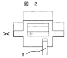
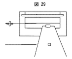
- FIGS. 1 to 6 show views from directly above the sample, and FIGS. 9 to 14 show cross-sectional views.
- the mark 1 on the substrate is detected by image recognition in a state where the sample is horizontal, and the periphery of the sample extraction unit 3 is automatically sputtered by the relative coordinates registered with respect to the mark 1 on the substrate.
- a state in which the formation of the holes 4 has been completed is shown.
- the sample extraction part 3 has a thin wall shape connected to the substrate only at the bottom.
- the relative position of the on-sample mark 2 with respect to the on-substrate mark 1 is determined in advance, and after the on-substrate mark 1 is formed, the on-sample mark 2 is automatically placed on the sample extraction portion 3 based on the on-substrate mark 1. It is processed with.
- the present invention is not limited to this, and the substrate mark 1 and the sample mark 2 may be processed together.
- the mark is created by sputtering by focused ion beam irradiation, but may be created by deposition or the like.
- the mark shape is not particularly limited as long as it is a size that can be processed on the sample, and a cross mark is used in this embodiment. When a similar shape exists on the sample surface, different mark shapes may be used in consideration of erroneous detection.
- the on-substrate mark 1 and the on-sample mark 2 have the same vertical position, but this is not necessarily important, and if they are included in the same scanning range, they must have a specific positional relationship. There is no. Moreover, the above-mentioned mark can be substituted with a clear feature existing in advance on the substrate.
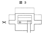
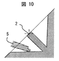
- the sample stage is inclined 45 ° and the sample extraction probe 5 is brought into contact with the substrate.
- the relationship between the initial coordinates on the probe tip image and the coordinate information of the probe drive mechanism is calibrated in advance. If the on-substrate mark 1 is detected by image recognition, it can be moved from the initial position of the probe to the target point according to the position information. Here, the probe tip is moved to the vicinity of the center of the front processing hole.
- the coordinates of the processing hole are known from the processing data, and the probe lowering position can be easily calculated by adding correction due to the sample inclination.
- FIGS. 2 and 3 show the positional relationship between the probe and the sample at this time.
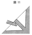
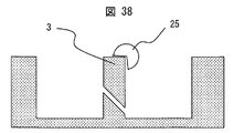
- FIG. 11 when the probe is moved vertically upward, the tip of the probe comes into contact with the thin wall because the thin wall of the extraction portion is inclined.
- the contact surface between the probe and the sample is almost determined by the tip step shape and the spring property of the probe.
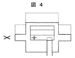
- the positional relationship between the sample and the probe at this time is shown in FIGS.
- the deposition gas is introduced by the nozzle to cause FIB-induced deposition around the contact surface.
- a probe and a sample can be adhere
- the positional relationship is likely to change due to the deformation of the tip, and the contact area is small. Therefore, the margin of the bonding process is small, and accurate positioning by the operator is required.
- the contact area can be secured by the above moving procedure and the probe step shape, so that accurate positioning becomes unnecessary.
- a tungsten deposited film by FIB induced deposition is used.
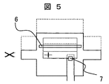
- the adhesion position on the extracted sample at this time may be determined based on either the on-substrate mark 1 or the on-sample mark 2. However, it is desirable that the deposited film is placed on the mark 2 on the sample and does not hinder mark detection.
- the relative position of the on-substrate mark 1 and the on-sample mark 2 in this state is the origin of displacement measurement for detecting the processing end point. Since both the mark 1 on the substrate and the mark 2 on the sample are registered in a state where the sample is horizontal, the shape when the sample is inclined 45 ° is cos (45 °) in the vertical direction of the screen. The image is shrunk to double, that is, 1 / ⁇ 2. However, since it is possible to collate with the original image by performing image processing, there is no problem in detecting the relative position.
- the coordinates of the processing pattern 6 in this step can be determined based on any of the on-substrate mark 1 and the on-sample mark 2. Since the thickness and width of the sample extraction portion are known, the size of the processing region can be determined by calculation from the coordinates and size of the peripheral processing pattern. Since the volume that must be removed by sputtering can be easily calculated, if the effects of the sputtering rate and the incident angle of the beam are reflected in the calculation, an approximate value of the processing time can be obtained using the probe current value of the FIB used for processing. It is done.
- the dimensions of the processing pattern are 1.5 microns in length and 15 microns in width, and the thickness of the thin wall of the extracted sample is 3 microns. Therefore, the volume is 95 considering the inclination angle of 45 °. .5 cubic microns.
- the processing volume per charge when tilted by 45 ° is known for gallium FIB with an acceleration energy of 30 keV and is 0.74 cubic microns / nC, so the required amount of charge is 129 nC.
- the probe current is 0.75 nA
- the calculation time is 172 seconds.
- the bottom-cutting hole 8 is close to the bottom of the peripheral processing hole 4, and the hole width is small compared to the thickness of the sample extraction portion, so that a high aspect ratio. It becomes the slot processing of.
- a phenomenon occurs in which the substance sputtered by the ion beam adheres to the separation processing portion as the redeposition film 10, and the processing speed is lower than the calculation. Therefore, it is technically difficult to stop the ion beam at the processing end point by managing only the beam irradiation time. Conventionally, when manually performed by an operator, the change in secondary electron intensity during processing was confirmed, or the processing was temporarily stopped and the secondary electron image was actually viewed to confirm whether or not they were separated. .
- the processing time is set to 10-20% longer than the calculation time and overetching is performed.
- the side wall near the hole outlet on the lower side of the sample is sputter processed. Therefore, reattachment occurs not only on the inner wall of the processed hole as shown in FIG. 8 but also on the back surface of the sample extraction portion on the side through which the processed hole passes, and must be removed again. Further, as shown in FIG. 8, there may be a case where the reattachment film 10 adheres the extraction portion and the inner surface of the hole and cannot be separated.
- a method of processing while spraying an etching gas containing a fluorine-based compound is effective for reducing redeposition.
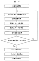
- the end point of the sample separation process is detected by measuring the relative position of the mark 1 on the substrate and the mark 2 on the sample.
- the processing time obtained from the calculation of the sputtering rate is 172 seconds as described above, but once every 20 seconds after 120 seconds, the ion beam scanning range is expanded from the sputter processing pattern to the entire region, and from the whole image.
- the registered image of each mark obtained before the start of processing is detected, and the relative position is measured. This procedure is shown in FIG. If the size of the image scanning area is 50 ⁇ m in length and width and the number of pixels is 512 ⁇ 512 in width and width, the pixel size is about 0.1 ⁇ m. Degree.
- separation processing with a high yield can be performed by detecting the relative position change between the extracted sample and the substrate by image recognition, detecting the processing end point, and stopping the FIB processing. Further, by detecting the movement of a minute sample at the processing end point using image recognition, the end point of separation processing by FIB processing can be detected mechanically regardless of human judgment. In addition, by forming marks on the extracted sample and the substrate in advance, the image recognition accuracy of a minute relative position movement between the substrate and the extracted sample is improved. Further, by providing a step shape at the probe tip, the positional relationship between the probe and the sample is limited.
- Adding a function to give the sample stage on which the substrate is mounted and the probe a minute displacement relative to the probe is added to the movement mechanism of the sample stage and / or the probe position control mechanism to expand the movement of the minute sample. And it is happening with good reproducibility. Further, by adding to the apparatus a function of stopping the beam scanning of the FIB apparatus being processed by detecting the relative position, over-etching from the detection of the processing end point is prevented.
- the separation of the sample from the substrate using focused ion beam irradiation and the adhesion and fixation of the extracted sample to the sample carrier are performed consistently and automatically.
- the difference from the first embodiment will be mainly described.
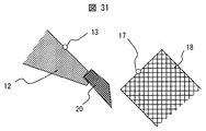
- FIG. 17 shows the marked probe 12 used in this embodiment.
- the marked probe 12 has an on-probe mark 13 formed on the upper surface thereof.
- FIG. 18 shows a cross-sectional shape of the probe. There is a step at the tip, and the contact between the probe and the sample is not a point but on a line segment along the sample, so the margin of the bonding process is large.
- the initial position registration of the probe is performed manually by the operator.
- the relative positional relationship between the probe mark 13 and the probe tip points 14 and 15 is registered on the image of FIG.
- the probe tip is adjusted in advance so as to be almost the same height as the sample surface. For this adjustment, first prepare a reference sample stage separately from the sample, obtain the eucentric height that does not change in height when tilted, and then contact the reference sample stage and the probe. This is done by confirming the secondary electron image of the FIB. This is defined as the reference height of the probe.
- the probe is moved in the X direction and Y direction of the probe driving mechanism, and the mark position on the probe is detected in the same manner.
- the conversion relationship between the coordinates of the probe driving mechanism and the pixel coordinates on the screen can be calculated.
- the center position of the FIB scan image and the origin position of the probe drive mechanism are not usually coincident and may rotate. Also, the display magnification of the screen is not accurate. Therefore, when the probe is driven based on the FIB scan image, this initial calibration is performed to obtain a conversion formula (generally a primary formula) between the pixel coordinates of the image and the coordinates of the drive mechanism.
- the peripheral processing is performed at a plurality of points on the substrate.
- the peripheral processing pattern is arranged with reference to the mark on the substrate.
- the peripheral machining shapes at all machining points are registered in the control device.
- the height of each point on the sample surface changes due to the tilt and warp of the sample, and the relative distance from the probe varies. Therefore, the height of the sample stage is adjusted at each processing point, and the coordinates are registered in the control device. .
- the height of the stage is so-called centric adjustment that moves so as to cancel the movement distance due to the tilt.
- an observation image using a FIB with a shallow depth of focus it is possible to substitute the focus by moving the stage.
- FIG. 19 shows a state in which the sample stage is moved to the registered coordinates of the first processing point with the probe retracted, the mark 1 on the substrate is detected, the stage height is lowered by 30 microns, and then the probe is inserted. It is a secondary electron image at the reference height. Since the height reproduction accuracy of the used sample stage and the probe drive mechanism is ⁇ 2 microns, the sample and the probe do not collide even if this operation is performed.
- the pixel coordinates of the probe tip within the screen are obtained from the probe tip point, that is, the 14 and 15 registration data in the FIB scan image of FIG. It is done. For this reason, since the position of the thin wall and the peripheral processing hole as the extracted sample can be determined from the coordinates of the mark 1 on the substrate and the processing pattern data of the peripheral processing registered at this point, the tip of the probe is the same as that of the first embodiment.
- the coordinates of the drive mechanism are set so as to be on the center of the front hole for peripheral machining. At this time, pixel coordinates obtained in advance and a coordinate conversion formula of the probe driving mechanism are used.
- the probe tip could be moved over the peripheral processing hole of the processed sample with an XY accuracy of ⁇ 0.2 ⁇ m of the probe moving mechanism.
- the probe is brought into contact with the substrate.
- the position detection of the on-probe mark 13 based on the FIB scanning image and the operation of raising the stage in steps of 2 microns are alternately performed. Since the position of the probe upper mark 13 changes due to the contact between the substrate and the probe, the contact is detected by detecting the displacement and the operation is stopped. While the stage is moving, if the probe vibrates due to the vibration generated by the drive motor, contact may be detected by mistake even though it is not in contact. Detect marks on the probe. After detecting the contact, the sample height is moved to the coordinate one step before the contact, and it is confirmed that the on-probe mark 13 has returned to the initial position, and the operation is terminated.
- the displacement detection method has an advantage that it can be used even when the substrate surface is insulative.
- the initial positions of the substrate mark 1 and the probe mark 13 are detected (FIG. 20). Since the substrate and the probe are in contact and the sample surface is almost at the eucentric height, there is almost no influence of the focus shift.
- the sample stage while reciprocating the sample stage in the vertical direction of FIG. 20, that is, in the axial direction of the probe with a width of 0.5 microns, the sample stage is moved downward by 0.5 micron steps, and the probe is gradually moved to the sample extraction portion.
- Move closer to. 21 and 22 show the positional relationship between the probe 12 and the sample extraction unit 3 as viewed from the cross-sectional direction.
- the ion beam is scanned on the mark in accordance with the reciprocation period, an image is captured, and the relative position between the substrate mark 1 and the probe mark 13 is measured.
- the probe since the probe may come into contact with the peripheral processing hole edge, the probe may move according to the sample movement. However, when the probe is reciprocated, it returns to the same position due to the spring property. However, the relative position becomes constant when the extracted sample comes into contact with the probe tip.
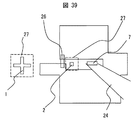
- FIG. 23 shows the relative coordinate change
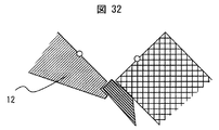
- FIG. 24 shows the positional relationship between the probe 12 and the sample. Since the tip position of the probe 12 with respect to the on-probe mark 13 is first calibrated, the probe can be brought into direct contact with the sample extraction portion, but the peripheral processing may not be performed in accordance with the pattern.
- FIG. 26 shows the cross section.
- the probe and the extracted sample are bonded.
- the probe adhesion deposition film 7 is arranged with reference to the on-probe mark 13, but the angle of the probe 12 may be slightly changed from the time of registration in FIG. 17 due to contact with the sample. Contains slight errors. For this reason, the pattern is made about twice as large in the vertical direction to absorb this error.
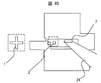
- the FIB is irradiated into the bottom cut pattern 6 while monitoring the relative positions of the substrate mark 1 and the probe mark 13 at regular intervals, and the bottom cut process is executed, thereby removing the sample. Is removed from the substrate. If the probe 12 is close to the substrate in this process, the distance between the sample and the substrate during processing is difficult to open. For this reason, if the probe is moved downward on the screen after bonding or if the inclination angle of the sample is reduced by about 0.5 to 1 °, the detection success rate of bottoming processing increases.
- the process moves to the step of fixing the extracted sample to the sample carrier.
- the probe to which the extracted sample is bonded is retracted to a position 50 microns higher than the eucentric height, and the stage on which the substrate is placed is also retracted, another stage on which a sample carrier for fixing the extracted sample is mounted is inserted, Move to the eucentric position.
- the sample carrier is a convex mesh for a transmission electron microscope.
- the sample carrier may be placed on the same stage as the sample. However, fixed positions are determined in advance, coordinates are registered, alignment marks are formed, and eucentric adjustment is performed.
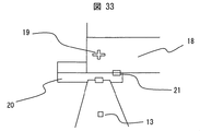
- the probe 12 is returned to the reference height, and the sample carrier 18 is tilted 45 ° eucentric in the same direction as the extracted sample 20.
- On the sample carrier 18, an on-carrier mark 19 is prepared in advance at a certain distance from the edge, and a mark image is registered and detected.
- the height deviation between the extracted sample and the carrier is the sum of the height of the extracted sample 20 and the mechanical error ⁇ 2 microns. Degree.
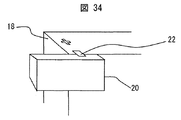
- the extracted sample 20 is fixed to the side surface instead of the upper end of the sample carrier.
- the final coordinates of the probe driving mechanism or the sample carrier stage mechanism at the fixed position Calculate and set What is important here is that the excised sample is slightly higher than the upper surface of the sample carrier. Otherwise, since the FIB cannot be irradiated to the bonding portion between the sample carrier and the extracted sample, the bonding strength is weakened. Finally, the probe adhesion deposit film 7 used for bonding the probe is removed by FIB sputtering to separate the probe and the extracted sample. The probe tip and the extracted sample may be separated by cutting the probe tip and the extracted sample by FIB sputtering.
- FIG. 34 shows the shape of the extracted sample after bonding
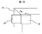
- FIG. 35 shows the shape of the sample during the thinning process. As can be seen from FIG. 35, only the portion that does not overlap with the sample carrier can be observed with a transmission electron microscope after being thinned. Although the observable range is wider when the fixed position is the end of the extracted sample, it is desirable to overlap the sample carrier with a few microns in consideration of the yield of the automatic process.
- the sample carrier is withdrawn.
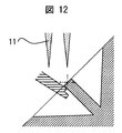
- the unnecessary probe adhesion deposition film attached to the probe is removed by sputtering. This step is performed based on the probe mark 13.
- the on-probe mark 13 is used as a reference, but the on-sample mark 2 may be used instead.
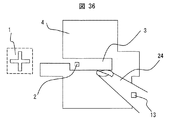
- the degree of freedom of movement of the probe is three directions of XYZ, but in this embodiment, a rotating probe having a degree of freedom of rotation around the probe axis is used.
- a rotating probe having a degree of freedom of rotation around the probe axis is used.
- FIG. 36 shows a state in which the tip of the rotary probe 24 is brought into contact with the extracted sample after the peripheral processing has been completed, as in the above embodiment.
- the tip of the rotating probe is calibrated with respect to the probe mark 13 by a manual operation by the same process as in the second embodiment.
- the contact between the probe and the substrate is also detected by alternately stepping the sample stage upward and monitoring the position of the probe mark 13. Since the insertion direction of the probe is from the lower right side, in this sample, the lower right side of the peripheral processing is sufficiently widened in advance, and there is no interference between the rotating probe 24 and the peripheral processing hole 4.
- this sample has already finished the automatic bottom cutting process, and has a cantilever shape. For this reason, even if it does not incline a stage, a separation process is possible by sputter-processing the connection part with the board
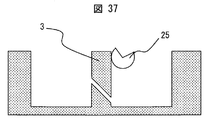
- the tip of the rotary probe is provided with a step shape corresponding to the convex portion of the sample, but has a surface inclined with respect to the rotation axis of the probe.
- the sample is caught by rotating as shown in FIG.
- This operation process is shown in FIG. 37 and FIG.
- the first contact surface is a conical surface
- the step shape is directed to the sample side by rotation, and the probe is pressed. Therefore, the step portion of the probe is applied to the corner of the upper surface of the sample by rotation of about 180 degrees. It becomes difficult to do.
- the upper surface and the stepped surface of the probe are in close contact with each other, and a stable positional relationship can be created as in the above-described stepped probe.
- a rectangle 27 shown by a broken line in FIG. 39 is a FIB scanning range at the time of mark position measurement, and is an area where the mark position is monitored by partially scanning the FIB during processing. Since the mark 2 moves with the end of the separation due to the stress caused by the probe rotation, the separation processing is stopped upon detecting this.
- the subsequent steps of extracting the sample and fixing it to the sample carrier are the same as in the previous embodiment.
- Unmanned micro sample preparation is possible, and the actual operating time of the device can be greatly extended.
- the number of semiconductor device failure analysis samples can be increased, and the yield of semiconductor devices can be improved efficiently and production management can be performed.
Landscapes
- Physics & Mathematics (AREA)
- Health & Medical Sciences (AREA)
- Life Sciences & Earth Sciences (AREA)
- Chemical & Material Sciences (AREA)
- Analytical Chemistry (AREA)
- Biochemistry (AREA)
- General Health & Medical Sciences (AREA)
- General Physics & Mathematics (AREA)
- Immunology (AREA)
- Pathology (AREA)
- Sampling And Sample Adjustment (AREA)
Priority Applications (1)
| Application Number | Priority Date | Filing Date | Title |
|---|---|---|---|
| US13/203,807 US8710464B2 (en) | 2009-03-30 | 2009-10-23 | Specimen preparation device, and control method in specimen preparation device |
Applications Claiming Priority (2)
| Application Number | Priority Date | Filing Date | Title |
|---|---|---|---|
| JP2009080851A JP5537058B2 (ja) | 2009-03-30 | 2009-03-30 | 試料作製装置、及び試料作製装置における制御方法 |
| JP2009-080851 | 2009-03-30 |
Publications (1)
| Publication Number | Publication Date |
|---|---|
| WO2010116428A1 true WO2010116428A1 (ja) | 2010-10-14 |
Family
ID=42935741
Family Applications (1)
| Application Number | Title | Priority Date | Filing Date |
|---|---|---|---|
| PCT/JP2009/005580 Ceased WO2010116428A1 (ja) | 2009-03-30 | 2009-10-23 | 試料作製装置、及び試料作製装置における制御方法 |
Country Status (3)
| Country | Link |
|---|---|
| US (1) | US8710464B2 (enExample) |
| JP (1) | JP5537058B2 (enExample) |
| WO (1) | WO2010116428A1 (enExample) |
Cited By (3)
| Publication number | Priority date | Publication date | Assignee | Title |
|---|---|---|---|---|
| JP2016105077A (ja) * | 2014-11-07 | 2016-06-09 | エフ・イ−・アイ・カンパニー | 自動化されたtem試料調製 |
| JP2018116865A (ja) * | 2017-01-19 | 2018-07-26 | 株式会社日立ハイテクサイエンス | 荷電粒子ビーム装置 |
| JP2020139958A (ja) * | 2014-06-30 | 2020-09-03 | 株式会社日立ハイテクサイエンス | 自動試料作製装置および自動試料作製方法 |
Families Citing this family (6)
| Publication number | Priority date | Publication date | Assignee | Title |
|---|---|---|---|---|
| US8759765B2 (en) * | 2011-08-08 | 2014-06-24 | Omniprobe, Inc. | Method for processing samples held by a nanomanipulator |
| CN105203364B (zh) * | 2015-10-27 | 2017-12-29 | 山东省科学院海洋仪器仪表研究所 | 海水中有机污染物富集装置及富集方法 |
| JP6931214B2 (ja) * | 2017-01-19 | 2021-09-01 | 株式会社日立ハイテクサイエンス | 荷電粒子ビーム装置 |
| JP7109051B2 (ja) * | 2018-03-30 | 2022-07-29 | 株式会社日立ハイテクサイエンス | 荷電粒子ビーム装置 |
| JP7308710B2 (ja) * | 2019-09-25 | 2023-07-14 | 株式会社日立ハイテクサイエンス | 集束イオンビーム装置 |
| CN111812124B (zh) * | 2020-06-24 | 2023-06-13 | 上海华力集成电路制造有限公司 | 一种失效分析去层方法 |
Citations (9)
| Publication number | Priority date | Publication date | Assignee | Title |
|---|---|---|---|---|
| JPH09306402A (ja) * | 1996-05-14 | 1997-11-28 | Hitachi Ltd | イオンビーム制限絞り板、マスク、集束イオンビーム装置及び投射型イオンビーム装置 |
| JP2000251820A (ja) * | 1999-03-04 | 2000-09-14 | Hitachi Ltd | マニピュレータおよびそれを用いたプローブ装置、試料作製装置 |
| JP2002040107A (ja) * | 2000-07-24 | 2002-02-06 | Hitachi Ltd | プローブ駆動方法及びプローブ装置 |
| JP2002150983A (ja) * | 2000-11-09 | 2002-05-24 | Jeol Ltd | マニピュレータ |
| JP2005345347A (ja) * | 2004-06-04 | 2005-12-15 | Hitachi High-Technologies Corp | 微小試料作製装置、微小試料設置具及び微小試料加工方法 |
| JP2007108042A (ja) * | 2005-10-14 | 2007-04-26 | Hitachi High-Technologies Corp | 試料解析方法及び試料加工装置 |
| JP2007194096A (ja) * | 2006-01-20 | 2007-08-02 | Hitachi High-Technologies Corp | 荷電粒子ビーム装置、及び荷電粒子ビーム装置を用いた試料のピックアップ方法 |
| JP2008026312A (ja) * | 2006-06-23 | 2008-02-07 | Fei Co | 平面ビュー・サンプル作製 |
| JP2008122114A (ja) * | 2006-11-09 | 2008-05-29 | Sii Nanotechnology Inc | Fibによるアトムプローブ分析用試料の作製方法とそれを実施する装置 |
Family Cites Families (11)
| Publication number | Priority date | Publication date | Assignee | Title |
|---|---|---|---|---|
| JP2774884B2 (ja) | 1991-08-22 | 1998-07-09 | 株式会社日立製作所 | 試料の分離方法及びこの分離方法で得た分離試料の分析方法 |
| EP0927880A4 (en) | 1997-07-22 | 2010-11-17 | Hitachi Ltd | METHOD AND DEVICE FOR PREPARING SAMPLES |
| US6828566B2 (en) * | 1997-07-22 | 2004-12-07 | Hitachi Ltd | Method and apparatus for specimen fabrication |
| JP3695181B2 (ja) | 1998-11-20 | 2005-09-14 | 株式会社日立製作所 | 基板抽出方法及びそれを用いた電子部品製造方法 |
| JP3843637B2 (ja) * | 1999-02-23 | 2006-11-08 | 株式会社日立製作所 | 試料作製方法および試料作製システム |
| EP1209737B2 (en) * | 2000-11-06 | 2014-04-30 | Hitachi, Ltd. | Method for specimen fabrication |
| JP4135143B2 (ja) * | 2003-04-22 | 2008-08-20 | 株式会社島津製作所 | 基板検査装置 |
| TWI255339B (en) * | 2004-12-23 | 2006-05-21 | Powerchip Semiconductor Corp | Method of applying micro-protection in defect analysis |
| US7312448B2 (en) * | 2005-04-06 | 2007-12-25 | Carl Zeiss Nts Gmbh | Method and apparatus for quantitative three-dimensional reconstruction in scanning electron microscopy |
| JP2007018935A (ja) * | 2005-07-08 | 2007-01-25 | Hitachi High-Technologies Corp | プローブ付き顕微鏡及びプローブ接触方法 |
| EP2106555B1 (en) * | 2006-10-20 | 2015-01-07 | FEI Company | Method for s/tem sample analysis |
-
2009
- 2009-03-30 JP JP2009080851A patent/JP5537058B2/ja not_active Expired - Fee Related
- 2009-10-23 WO PCT/JP2009/005580 patent/WO2010116428A1/ja not_active Ceased
- 2009-10-23 US US13/203,807 patent/US8710464B2/en not_active Expired - Fee Related
Patent Citations (9)
| Publication number | Priority date | Publication date | Assignee | Title |
|---|---|---|---|---|
| JPH09306402A (ja) * | 1996-05-14 | 1997-11-28 | Hitachi Ltd | イオンビーム制限絞り板、マスク、集束イオンビーム装置及び投射型イオンビーム装置 |
| JP2000251820A (ja) * | 1999-03-04 | 2000-09-14 | Hitachi Ltd | マニピュレータおよびそれを用いたプローブ装置、試料作製装置 |
| JP2002040107A (ja) * | 2000-07-24 | 2002-02-06 | Hitachi Ltd | プローブ駆動方法及びプローブ装置 |
| JP2002150983A (ja) * | 2000-11-09 | 2002-05-24 | Jeol Ltd | マニピュレータ |
| JP2005345347A (ja) * | 2004-06-04 | 2005-12-15 | Hitachi High-Technologies Corp | 微小試料作製装置、微小試料設置具及び微小試料加工方法 |
| JP2007108042A (ja) * | 2005-10-14 | 2007-04-26 | Hitachi High-Technologies Corp | 試料解析方法及び試料加工装置 |
| JP2007194096A (ja) * | 2006-01-20 | 2007-08-02 | Hitachi High-Technologies Corp | 荷電粒子ビーム装置、及び荷電粒子ビーム装置を用いた試料のピックアップ方法 |
| JP2008026312A (ja) * | 2006-06-23 | 2008-02-07 | Fei Co | 平面ビュー・サンプル作製 |
| JP2008122114A (ja) * | 2006-11-09 | 2008-05-29 | Sii Nanotechnology Inc | Fibによるアトムプローブ分析用試料の作製方法とそれを実施する装置 |
Cited By (9)
| Publication number | Priority date | Publication date | Assignee | Title |
|---|---|---|---|---|
| JP2020139958A (ja) * | 2014-06-30 | 2020-09-03 | 株式会社日立ハイテクサイエンス | 自動試料作製装置および自動試料作製方法 |
| US11073453B2 (en) | 2014-06-30 | 2021-07-27 | Hitachi High-Tech Science Corporation | Automatic sample preparation apparatus and automatic sample preparation method |
| JP7008355B2 (ja) | 2014-06-30 | 2022-01-25 | 株式会社日立ハイテクサイエンス | 自動試料作製装置および自動試料作製方法 |
| JP2022033241A (ja) * | 2014-06-30 | 2022-02-28 | 株式会社日立ハイテクサイエンス | 試料作製装置 |
| JP7266322B2 (ja) | 2014-06-30 | 2023-04-28 | 株式会社日立ハイテクサイエンス | 試料作製装置 |
| US11835438B2 (en) | 2014-06-30 | 2023-12-05 | Hitachi High-Tech Science Corporation | Automatic sample preparation apparatus |
| JP2016105077A (ja) * | 2014-11-07 | 2016-06-09 | エフ・イ−・アイ・カンパニー | 自動化されたtem試料調製 |
| US10340119B2 (en) | 2014-11-07 | 2019-07-02 | Fei Company | Automated TEM sample preparation |
| JP2018116865A (ja) * | 2017-01-19 | 2018-07-26 | 株式会社日立ハイテクサイエンス | 荷電粒子ビーム装置 |
Also Published As
| Publication number | Publication date |
|---|---|
| US20110309245A1 (en) | 2011-12-22 |
| JP5537058B2 (ja) | 2014-07-02 |
| JP2010230612A (ja) | 2010-10-14 |
| US8710464B2 (en) | 2014-04-29 |
Similar Documents
| Publication | Publication Date | Title |
|---|---|---|
| JP5537058B2 (ja) | 試料作製装置、及び試料作製装置における制御方法 | |
| US10825651B2 (en) | Automated TEM sample preparation | |
| JP6586261B2 (ja) | 大容量temグリッド及び試料取り付け方法 | |
| KR102522414B1 (ko) | 하전 입자 빔 장치 | |
| EP2068160A2 (en) | Apparatus and method for observing defects in semiconductor wafers | |
| TWI758356B (zh) | 帶電粒子束裝置 | |
| CN110335800B (zh) | 带电粒子束装置 | |
| KR20190056966A (ko) | 하전 입자 빔 장치 | |
| KR101550921B1 (ko) | 단면 가공 방법 및 장치 | |
| JP6700897B2 (ja) | 荷電粒子ビーム装置 | |
| JP6542608B2 (ja) | 荷電粒子ビーム装置 | |
| TW201643927A (zh) | 針對自動s/tem擷取及計量學而使用已知形狀的層狀物之型樣匹配 | |
| KR102358551B1 (ko) | 자동 시료편 제작 장치 | |
| US10410829B1 (en) | Methods for acquiring planar view stem images of device structures | |
| JP6105530B2 (ja) | 自動試料片作製装置 | |
| US10539489B2 (en) | Methods for acquiring planar view STEM images of device structures | |
| JP6885637B2 (ja) | 荷電粒子ビーム装置 | |
| JP2016050854A (ja) | 自動試料片作製装置 | |
| JP2008014899A (ja) | 試料作製方法 |
Legal Events
| Date | Code | Title | Description |
|---|---|---|---|
| 121 | Ep: the epo has been informed by wipo that ep was designated in this application |
Ref document number: 09842938 Country of ref document: EP Kind code of ref document: A1 |
|
| WWE | Wipo information: entry into national phase |
Ref document number: 13203807 Country of ref document: US |
|
| NENP | Non-entry into the national phase |
Ref country code: DE |
|
| 122 | Ep: pct application non-entry in european phase |
Ref document number: 09842938 Country of ref document: EP Kind code of ref document: A1 |