WO2010110304A1 - Molded body, method for producing same, electronic device member, and electronic device - Google Patents
Molded body, method for producing same, electronic device member, and electronic device Download PDFInfo
- Publication number
- WO2010110304A1 WO2010110304A1 PCT/JP2010/055064 JP2010055064W WO2010110304A1 WO 2010110304 A1 WO2010110304 A1 WO 2010110304A1 JP 2010055064 W JP2010055064 W JP 2010055064W WO 2010110304 A1 WO2010110304 A1 WO 2010110304A1
- Authority
- WO
- WIPO (PCT)
- Prior art keywords
- layer
- electronic device
- polymer layer
- ion implantation
- plasma
- Prior art date
Links
Images

Classifications
-
- C—CHEMISTRY; METALLURGY
- C23—COATING METALLIC MATERIAL; COATING MATERIAL WITH METALLIC MATERIAL; CHEMICAL SURFACE TREATMENT; DIFFUSION TREATMENT OF METALLIC MATERIAL; COATING BY VACUUM EVAPORATION, BY SPUTTERING, BY ION IMPLANTATION OR BY CHEMICAL VAPOUR DEPOSITION, IN GENERAL; INHIBITING CORROSION OF METALLIC MATERIAL OR INCRUSTATION IN GENERAL
- C23C—COATING METALLIC MATERIAL; COATING MATERIAL WITH METALLIC MATERIAL; SURFACE TREATMENT OF METALLIC MATERIAL BY DIFFUSION INTO THE SURFACE, BY CHEMICAL CONVERSION OR SUBSTITUTION; COATING BY VACUUM EVAPORATION, BY SPUTTERING, BY ION IMPLANTATION OR BY CHEMICAL VAPOUR DEPOSITION, IN GENERAL
- C23C14/00—Coating by vacuum evaporation, by sputtering or by ion implantation of the coating forming material
- C23C14/22—Coating by vacuum evaporation, by sputtering or by ion implantation of the coating forming material characterised by the process of coating
- C23C14/48—Ion implantation
-
- C—CHEMISTRY; METALLURGY
- C08—ORGANIC MACROMOLECULAR COMPOUNDS; THEIR PREPARATION OR CHEMICAL WORKING-UP; COMPOSITIONS BASED THEREON
- C08J—WORKING-UP; GENERAL PROCESSES OF COMPOUNDING; AFTER-TREATMENT NOT COVERED BY SUBCLASSES C08B, C08C, C08F, C08G or C08H
- C08J7/00—Chemical treatment or coating of shaped articles made of macromolecular substances
- C08J7/04—Coating
- C08J7/048—Forming gas barrier coatings
-
- C—CHEMISTRY; METALLURGY
- C08—ORGANIC MACROMOLECULAR COMPOUNDS; THEIR PREPARATION OR CHEMICAL WORKING-UP; COMPOSITIONS BASED THEREON
- C08J—WORKING-UP; GENERAL PROCESSES OF COMPOUNDING; AFTER-TREATMENT NOT COVERED BY SUBCLASSES C08B, C08C, C08F, C08G or C08H
- C08J7/00—Chemical treatment or coating of shaped articles made of macromolecular substances
- C08J7/04—Coating
- C08J7/06—Coating with compositions not containing macromolecular substances
-
- C—CHEMISTRY; METALLURGY
- C23—COATING METALLIC MATERIAL; COATING MATERIAL WITH METALLIC MATERIAL; CHEMICAL SURFACE TREATMENT; DIFFUSION TREATMENT OF METALLIC MATERIAL; COATING BY VACUUM EVAPORATION, BY SPUTTERING, BY ION IMPLANTATION OR BY CHEMICAL VAPOUR DEPOSITION, IN GENERAL; INHIBITING CORROSION OF METALLIC MATERIAL OR INCRUSTATION IN GENERAL
- C23C—COATING METALLIC MATERIAL; COATING MATERIAL WITH METALLIC MATERIAL; SURFACE TREATMENT OF METALLIC MATERIAL BY DIFFUSION INTO THE SURFACE, BY CHEMICAL CONVERSION OR SUBSTITUTION; COATING BY VACUUM EVAPORATION, BY SPUTTERING, BY ION IMPLANTATION OR BY CHEMICAL VAPOUR DEPOSITION, IN GENERAL
- C23C14/00—Coating by vacuum evaporation, by sputtering or by ion implantation of the coating forming material
- C23C14/06—Coating by vacuum evaporation, by sputtering or by ion implantation of the coating forming material characterised by the coating material
- C23C14/14—Metallic material, boron or silicon
- C23C14/20—Metallic material, boron or silicon on organic substrates
-
- C—CHEMISTRY; METALLURGY
- C23—COATING METALLIC MATERIAL; COATING MATERIAL WITH METALLIC MATERIAL; CHEMICAL SURFACE TREATMENT; DIFFUSION TREATMENT OF METALLIC MATERIAL; COATING BY VACUUM EVAPORATION, BY SPUTTERING, BY ION IMPLANTATION OR BY CHEMICAL VAPOUR DEPOSITION, IN GENERAL; INHIBITING CORROSION OF METALLIC MATERIAL OR INCRUSTATION IN GENERAL
- C23C—COATING METALLIC MATERIAL; COATING MATERIAL WITH METALLIC MATERIAL; SURFACE TREATMENT OF METALLIC MATERIAL BY DIFFUSION INTO THE SURFACE, BY CHEMICAL CONVERSION OR SUBSTITUTION; COATING BY VACUUM EVAPORATION, BY SPUTTERING, BY ION IMPLANTATION OR BY CHEMICAL VAPOUR DEPOSITION, IN GENERAL
- C23C14/00—Coating by vacuum evaporation, by sputtering or by ion implantation of the coating forming material
- C23C14/22—Coating by vacuum evaporation, by sputtering or by ion implantation of the coating forming material characterised by the process of coating
- C23C14/56—Apparatus specially adapted for continuous coating; Arrangements for maintaining the vacuum, e.g. vacuum locks
- C23C14/562—Apparatus specially adapted for continuous coating; Arrangements for maintaining the vacuum, e.g. vacuum locks for coating elongated substrates
-
- C—CHEMISTRY; METALLURGY
- C08—ORGANIC MACROMOLECULAR COMPOUNDS; THEIR PREPARATION OR CHEMICAL WORKING-UP; COMPOSITIONS BASED THEREON
- C08G—MACROMOLECULAR COMPOUNDS OBTAINED OTHERWISE THAN BY REACTIONS ONLY INVOLVING UNSATURATED CARBON-TO-CARBON BONDS
- C08G77/00—Macromolecular compounds obtained by reactions forming a linkage containing silicon with or without sulfur, nitrogen, oxygen or carbon in the main chain of the macromolecule
- C08G77/04—Polysiloxanes
-
- C—CHEMISTRY; METALLURGY
- C08—ORGANIC MACROMOLECULAR COMPOUNDS; THEIR PREPARATION OR CHEMICAL WORKING-UP; COMPOSITIONS BASED THEREON
- C08J—WORKING-UP; GENERAL PROCESSES OF COMPOUNDING; AFTER-TREATMENT NOT COVERED BY SUBCLASSES C08B, C08C, C08F, C08G or C08H
- C08J2383/00—Characterised by the use of macromolecular compounds obtained by reactions forming in the main chain of the macromolecule a linkage containing silicon with or without sulfur, nitrogen, oxygen, or carbon only; Derivatives of such polymers
- C08J2383/04—Polysiloxanes
Definitions
- the present invention relates to a molded article having excellent gas barrier properties, bending resistance, and surface smoothness, a method for producing the molded article, an electronic device member comprising the molded article, and an electronic device provided with the electronic device member.
- a polymer molded body such as a plastic film is inexpensive and excellent in workability, and therefore has been used in various fields with a desired function.
- a gas barrier plastic film that prevents the permeation of water vapor and oxygen is used for food and pharmaceutical packaging films in order to maintain the taste and freshness by suppressing the oxidation and alteration of proteins and fats and oils.
- the plastic film has a problem that it easily transmits water vapor, oxygen, and the like as compared with the glass plate, and easily causes deterioration of elements inside the display.
- Patent Document 1 proposes a flexible display substrate in which a transparent gas barrier layer made of a metal oxide is laminated on a transparent plastic film.
- the flexible display substrate described in this document is obtained by laminating a transparent gas barrier layer made of a metal oxide on the surface of a transparent plastic film by vapor deposition, ion plating, sputtering, or the like.
- vapor deposition ion plating, sputtering, or the like.
- the gas barrier layer is cracked and the gas barrier property is lowered.
- the surface smoothness of the gas barrier layer is inferior, and when other layers are formed on the gas barrier layer, pinholes are easily generated in the formed other layers, and sufficient reliability as an electronic device member cannot be obtained. There was a problem.
- Patent Document 2 discloses a gas barrier laminate obtained by laminating a plastic film and a resin layer containing polyorganosilsesquioxane as a main component on at least one surface of the plastic film.
- gas barrier properties such as oxygen and water vapor
- the present invention has been made in view of the above-described prior art, and is a molded body excellent in gas barrier properties, bending resistance, and surface smoothness, a manufacturing method thereof, an electronic device member comprising the molded body, and the electronic It is an object to provide an electronic device including a device member.
- the present inventors have found that a molded product having a layer containing a polyorganosiloxane compound on the surface, a silicon compound on the surface of the layer containing the polyorganosiloxane compound. It has been found that the molded body can be easily and efficiently produced by injecting ions, and the present invention has been completed by generalizing this knowledge.
- the following molded articles (1) to (4) are provided.
- a method for producing a molded article according to the following (5) to (8) there is provided a method for producing a molded article according to the following (5) to (8).
- the method for producing a molded article according to (1) including a step of injecting silicon compound ions into the surface portion of the polymer layer of the molded product having the polymer layer on the surface portion.
- the method for producing a molded article according to (2) including a step of injecting silicon compound ions into the surface portion of the polymer layer by a plasma ion implantation method on the molded portion having the polymer layer on the surface portion.
- silicon compound ions are implanted into the polymer layer while conveying a long molded product having the polymer layer on the surface in a certain direction.
- the manufacturing method of the molded object of description (8) The method for producing a molded article according to any one of (5) to (7), wherein the polymer layer is a layer containing a polyorganosiloxane compound.
- the following electronic device member (9) is provided.
- An electronic device member comprising the molded article according to any one of (1) to (4).
- the molded product of the present invention is excellent in gas barrier properties, flex resistance, and surface smoothness. Therefore, the molded object of this invention can be used suitably as members for electronic devices, such as a display and a solar cell. According to the production method of the present invention, the molded article of the present invention having excellent gas barrier properties, flex resistance, and surface smoothness can be produced safely, simply and efficiently. In addition, the area can be easily increased at a lower cost than the method of forming an inorganic film. Since the member for electronic devices of this invention is excellent in gas barrier property, bending resistance, and surface smoothness, it can be used suitably for electronic devices, such as a display and a solar cell.
- the molded product of the present invention is characterized by having a layer (hereinafter referred to as “ion-implanted layer”) obtained by implanting silicon compound ions into a polymer layer.
- the ion-implanted layer is not particularly limited as long as the ion of the silicon compound is implanted into the polymer layer.
- the polymer that forms the polymer layer is not particularly limited.
- Examples include polyphenylene sulfide, polyarylate, acrylic resin, cycloolefin polymer, aromatic polymer, and polyorganosiloxane compound. These polymers may be used alone or in combination of two or more.
- the polymer layer used in the present invention is preferably a polyester such as a polyorganosiloxane compound, polyethylene terephthalate, polybutylene terephthalate, or polyethylene naphthalate, and a molded article having excellent gas barrier properties can be obtained.
- a layer containing a compound is particularly preferred.
- the linear main chain structure is a structure represented by the following formula (a)
- the ladder main chain structure is a structure represented by the following formula (b): a cage main chain structure
- each of Rx, Ry, and Rz independently represents a hydrogen atom, an unsubstituted or substituted alkyl group, an unsubstituted or substituted alkenyl group, an unsubstituted or substituted aryl group, etc. Represents a hydrolyzable group.
- each of Rx in the formula (a) and Ry in the formula (b) is not a hydrogen atom.
- alkyl group of the unsubstituted or substituted alkyl group examples include, for example, methyl group, ethyl group, n-propyl group, isopropyl group, n-butyl group, isobutyl group, sec-butyl group, t-butyl group, n
- alkyl groups having 1 to 10 carbon atoms such as -pentyl group, isopentyl group, neopentyl group, n-hexyl group, n-heptyl group and n-octyl group.
- alkenyl group examples include alkenyl groups having 2 to 10 carbon atoms such as vinyl group, 1-propenyl group, 2-propenyl group, 1-butenyl group, 2-butenyl group and 3-butenyl group.
- substituent for the alkyl group and alkenyl group examples include a halogen atom such as a fluorine atom, a chlorine atom, a bromine atom and an iodine atom; a hydroxyl group; a thiol group; an epoxy group; a glycidoxy group; a (meth) acryloyloxy group; And a phenyl group having no substituent or a substituent such as a 4-methylphenyl group and a 4-chlorophenyl group.
- aryl group of an unsubstituted or substituted aryl group examples include aryl groups having 6 to 10 carbon atoms such as a phenyl group, a 1-naphthyl group, and a 2-naphthyl group.
- substituent of the aryl group examples include halogen atoms such as fluorine atom, chlorine atom, bromine atom and iodine atom; alkyl groups having 1 to 6 carbon atoms such as methyl group and ethyl group; carbon numbers such as methoxy group and ethoxy group 1-6 alkoxy groups; nitro groups; cyano groups; hydroxyl groups; thiol groups; epoxy groups; glycidoxy groups; (meth) acryloyloxy groups; unsubstituted phenyl groups, 4-methylphenyl groups, 4-chlorophenyl groups, etc.
- Rx, Ry, and Rz a hydrogen atom, an alkyl group having 1 to 6 carbon atoms, or a phenyl group is preferable, and an alkyl group having 1 to 6 carbon atoms is particularly preferable.
- the plurality of Rx in the formula (a), the plurality of Ry in the formula (b), and the plurality of Rz in the formula (c) may be the same or different.
- the polyorganosiloxane-based compound is preferably a linear compound represented by the formula (a) or a ladder-like compound represented by the formula (b). From the viewpoint of forming an ion-implanted layer having excellent gas barrier properties, polydimethylsiloxane in which two Rx in the formula (a) are both methyl groups is particularly preferable.
- the polyorganosiloxane compound can be obtained by a known production method in which a silane compound having a hydrolyzable functional group is polycondensed.
- the silane compound to be used may be appropriately selected according to the structure of the target polyorganosiloxane compound.
- Preferred specific examples include bifunctional silane compounds such as dimethyldimethoxysilane, dimethyldiethoxysilane, diethyldimethoxysilane, and diethyldiethoxysilane; methyltrimethoxysilane, methyltriethoxysilane, ethyltrimethoxysilane, ethyltriethoxysilane, trifunctional silane compounds such as n-propyltrimethoxysilane, n-butyltriethoxysilane, phenyltrimethoxysilane, phenyltriethoxysilane, phenyldiethoxymethoxysilane; tetramethoxysilane, tetraethoxysilane, tetra-n-propoxysilane, Tetraisopropoxysilane, tetra-
- polyorganosiloxane compound a commercially available product as a release agent, an adhesive, a sealant, a paint, or the like can be used as it is.
- the content of the polyorganosiloxane compound in the layer containing the polyorganosiloxane compound is preferably 50% by weight or more, and 70% by weight or more from the viewpoint of forming an ion-implanted layer having excellent gas barrier properties. It is more preferable that
- the polymer layer may contain other components in addition to the main component polymer compound as long as the object of the present invention is not impaired.
- other components include a curing agent, an anti-aging agent, a light stabilizer, and a flame retardant.
- a layer containing a polyorganosiloxane compound is obtained by applying a layer forming solution containing at least one polyorganosiloxane compound, optionally other components, and a solvent on a suitable substrate.
- the obtained coating film can be dried and formed by heating or the like as necessary.
- a film made of a material of another layer described later can be used as the substrate.
- the thickness of the layer containing the polyorganosiloxane compound to be formed is not particularly limited, but is usually 30 nm to 100 ⁇ m.
- the polymer layer a commercially available polymer film made of the polymer can be used.
- the ion-implanted layer is obtained by implanting ions of a silicon compound (hereinafter sometimes simply referred to as “ions”) into the polymer layer.
- ions a silicon compound
- Examples of the silicon compound include silane (SiH 4 ) and organosilicon compounds.
- organosilicon compound include tetraalkoxysilanes such as tetramethoxysilane, tetraethoxysilane, tetra n-propoxysilane, tetraisopropoxysilane, tetra n-butoxysilane, and tetra t-butoxysilane;
- An alkylalkoxysilane having an unsubstituted or substituted group such as dimethyldimethoxysilane, dimethyldiethoxysilane, diethyldimethoxysilane, methyltriethoxysilane, ethyltrimethoxysilane, (3,3,3-trifluoropropyl) trimethoxysilane;
- Arylalkoxysilanes such as diphenyldimethoxysilane and phenyltriethoxysilane
- disiloxane alkylsilane, tetraalkoxysilane, and silazane are preferable from the viewpoint of more easily obtaining the molded article targeted by the present invention.
- the ion implantation amount may be appropriately determined according to the intended use (necessary gas barrier property, transparency, etc.) of the formed article to be formed.
- the method for injecting ions into the polymer layer is not particularly limited. For example, after forming a layer containing a polyorganosiloxane compound on a substrate, ions of a silicon compound are injected into the layer containing the polyorganosiloxane compound. Methods and the like.
- Examples of the method of implanting ions include a method of irradiating ions accelerated by an electric field (ion beam), a method of implanting ions in plasma, and the like.
- ion beam an electric field
- plasma ion implantation method the latter method of implanting ions in plasma (hereinafter sometimes referred to as “plasma ion implantation method”) is preferable.
- plasma is generated in an atmosphere containing a silicon compound gas, and negative high voltage pulses are applied to the polymer layer to inject ions in the plasma into the surface of the polymer layer. Can be done.
- the thickness of the ion-implanted portion can be controlled by the implantation conditions, and may be appropriately determined according to the purpose of use of the molded body, but is usually 0.1 to 1000 nm.
- the shape of the molded product of the present invention is not particularly limited, and examples thereof include a film shape, a sheet shape, a rectangular parallelepiped shape, a polygonal column shape, and a cylindrical shape.
- a film shape When used as an electronic device member as described later, it is preferably a film or sheet.
- the thickness of the film can be appropriately determined depending on the intended use of the electronic device.
- the molded body of the present invention may be composed only of a polymer layer having an ion implantation layer, or may further include other layers.
- the other layer may be a single layer or two or more layers of the same type or different types.
- Examples of the material for the other layer include the same materials as those exemplified as the polymer used for the polymer layer into which the ions are implanted. Especially, since it is excellent in transparency and has versatility, a polyester, polyamide, or a cycloolefin type polymer is preferable, and a polyester or a cycloolefin type polymer is more preferable.
- polyester examples include polyethylene terephthalate, polybutylene terephthalate, polyethylene naphthalate, and polyarylate.
- polyamide examples include wholly aromatic polyamide, nylon 6, nylon 66, nylon copolymer, and the like.
- cycloolefin polymers include norbornene polymers, monocyclic olefin polymers, cyclic conjugated diene polymers, vinyl alicyclic hydrocarbon polymers, and hydrides thereof. Specific examples thereof include Apel (an ethylene-cycloolefin copolymer manufactured by Mitsui Chemicals), Arton (a norbornene polymer manufactured by JSR), Zeonoa (a norbornene polymer manufactured by Nippon Zeon), and the like. .
- Apel an ethylene-cycloolefin copolymer manufactured by Mitsui Chemicals
- Arton a norbornene polymer manufactured by JSR
- Zeonoa a norbornene polymer manufactured by Nippon Zeon
- the position of the ion-implanted layer is not particularly limited, but it is preferable to have the ion-implanted layer on the surface because it can be efficiently manufactured.
- the ion implantation layer may be formed only in the single side
- the molded article of the present invention preferably has excellent gas barrier properties, flex resistance, and surface smoothness, and the shape thereof is a film or sheet (hereinafter referred to as “film”).
- the molded article of the present invention has an excellent gas barrier property because the permeability of gas such as water vapor of the molded article of the present invention is much smaller than that in which ions are not implanted. Can be confirmed.
- the water vapor transmission rate in an atmosphere at 40 ° C. and 90% relative humidity that is, the amount of water vapor that passes through the molded body from the humidity control chamber side at 90% relative humidity at 40 ° C. is 1 g / m 2 / day. The following is preferable, and 0.5 g / m 2 / day or less is more preferable.
- the transmittance of the molded body such as water vapor can be measured using a known gas permeability measuring device.
- the molded body of the present invention has excellent bending resistance, for example, even if the molded body is wound around a stainless steel rod with the ion-implanted surface outside and is reciprocated 10 times in the circumferential direction. This can be confirmed by not deteriorating.
- the molded article of the present invention has excellent surface smoothness, for example, by measuring the surface roughness Ra value (nm) in the measurement region 1 ⁇ 1 ⁇ m and 25 ⁇ 25 ⁇ m using an atomic force microscope (AFM). It can confirm by measuring using.
- the Ra value at 1 ⁇ 1 ⁇ m is preferably 0.35 nm or less, more preferably 0.3 nm or less, and the Ra value at 25 ⁇ 25 ⁇ m is preferably 6 nm or less.
- the manufacturing method of the molded object of this invention has the process of inject
- a molded article is produced by injecting ions of a silicon compound into a polymer layer while conveying a long molded article having a polymer layer on the surface portion in a certain direction.
- ions can be injected while being conveyed in a certain direction, and can be wound up by a winding roll.
- the molded product obtained in this way can be continuously produced.
- the shape of the long molded product is a film, which may be a polymer layer alone or may include other layers. As the other layers, the same layers as those described above can be used.
- the thickness of the molded product is preferably 1 ⁇ m to 500 ⁇ m, more preferably 5 ⁇ m to 300 ⁇ m, from the viewpoint of unwinding, winding and conveying operability.
- the method for injecting ions into the polymer layer is not particularly limited. Among these, a method of forming an ion implantation layer on the surface portion of the layer by plasma ion implantation is preferable.
- a negative high-voltage pulse is applied to a molded article that has been exposed to plasma and has a polymer layer on its surface, whereby ions in the plasma are implanted into the surface portion of the layer.
- (A) a method in which ions existing in plasma generated using an external electric field are implanted into the surface portion of the layer, or (B) the layer is formed without using an external electric field.
- a method of injecting ions present in the plasma generated only by the electric field by the negative high voltage pulse to be applied to the surface portion of the layer is preferable.
- the pressure during ion implantation is preferably 0.01 to 1 Pa.
- the pressure during plasma ion implantation is in such a range, a uniform ion implantation layer can be easily and efficiently formed, and an ion implantation layer having both transparency and gas barrier properties can be efficiently formed. Can do.
- the processing operation is simple, and the processing time can be greatly shortened. Further, the entire layer can be processed uniformly, and ions in the plasma can be continuously injected into the surface portion of the layer with high energy when a negative high voltage pulse is applied. Furthermore, without applying special other means such as radio frequency (hereinafter abbreviated as “RF”) or a high frequency power source such as a microwave, just applying a negative high voltage pulse to the layer, A high-quality ion-implanted layer can be uniformly formed on the surface of the layer.
- RF radio frequency
- a high frequency power source such as a microwave
- the pulse width when applying a negative high voltage pulse is preferably 1 to 15 ⁇ sec.
- the pulse width is in such a range, a transparent and uniform ion implantation layer can be formed more easily and efficiently.
- the applied voltage when generating plasma is preferably -1 kV to -50 kV, more preferably -1 kV to -30 kV, and particularly preferably -5 kV to -20 kV. If ion implantation is performed at an applied voltage greater than ⁇ 1 kV, the ion implantation amount (dose amount) becomes insufficient, and desired performance cannot be obtained. On the other hand, if ion implantation is performed at a value smaller than ⁇ 50 kV, the molded body is charged at the time of ion implantation, and defects such as coloring of the molded body occur.
- a plasma ion implantation apparatus When ions in plasma are implanted into the surface portion of the layer, a plasma ion implantation apparatus is used. Specifically, as a plasma ion implantation apparatus, ( ⁇ ) a high-frequency power is superimposed on a feedthrough that applies a negative high-voltage pulse to a polymer layer (hereinafter also referred to as “ion-implanted layer”). A device that uniformly surrounds the periphery of the ion-implanted layer with plasma and attracts, implants, collides and deposits ions in the plasma (Japanese Patent Laid-Open No.
- a plasma ion implantation apparatus that generates plasma using an external electric field such as a high-frequency power source such as a microwave and applies high voltage pulses to attract and inject ions in the plasma
- a plasma ion implantation apparatus that implants ions in plasma generated only by an electric field generated by applying a high voltage pulse without using an external electric field.
- the plasma ion implantation apparatus ( ⁇ ) or ( ⁇ ) because the processing operation is simple, the processing time can be greatly shortened, and it is suitable for continuous use.
- a method using the plasma ion implantation apparatuses ( ⁇ ) and ( ⁇ ) will be described in detail with reference to the drawings.
- FIG. 1 is a diagram showing an outline of a continuous plasma ion implantation apparatus including the plasma ion implantation apparatus ( ⁇ ).
- 1a is a long film-like molded product (hereinafter referred to as “film”) having a polymer layer to be ion-implanted on its surface
- 11a is a chamber
- 20a is a turbo molecular pump
- 3a Is an unwinding roll for feeding out the film 1a before being ion-implanted
- 5a is a winding roll for winding the ion-implanted film (molded body) 1b into a roll shape
- 2a is a high-voltage applied rotation can
- 6a is a film-feeding roll.
- FIG. 1B is a perspective view of the high-voltage applying rotation can 2a, and 15 is a high-voltage introduction terminal (feedthrough).
- the long film 1a having a polymer layer used in the present embodiment on the surface is a film in which a polymer layer is formed on a base material (another layer).
- the film 1a is transported in the chamber 11a from the unwinding roll 3a in the direction of the arrow X in FIG. It is wound up on a roll 5a.
- the film 1a is transported by rotating the high voltage application rotating can 2a at a constant speed. ing.
- the rotation of the high voltage application rotation can 2a is performed by rotating the central shaft 13 of the high voltage introduction terminal 15 by a motor.
- the high voltage introduction terminal 15 and the plurality of delivery rolls 6a with which the film 1a comes into contact are made of an insulator, for example, formed by coating the surface of alumina with a resin such as polytetrafluoroethylene.
- the high-voltage applying rotation can 2a is made of a conductor and can be formed of, for example, stainless steel.
- the conveyance speed of the film 1a can be set as appropriate. If the film 1a is transported from the unwinding roll 3a and is wound on the take-up roll 5a, the film 1a is ion-implanted into the film 1a so that a time sufficient for forming a desired ion-implanted layer is secured. There are no particular restrictions.
- the film winding speed (line speed) is usually from 0.1 to 3 m / min, preferably from 0.2 to 2.5 m / min, although it depends on the applied voltage, the apparatus scale, and the like.
- the chamber 11a is evacuated by a turbo molecular pump 20a connected to a rotary pump to reduce the pressure.
- the degree of reduced pressure is usually 1 ⁇ 10 ⁇ 4 Pa to 1 Pa, preferably 1 ⁇ 10 ⁇ 3 Pa to 1 ⁇ 10 ⁇ 2 Pa.
- a gas for ion implantation such as trimethylsilane (hereinafter sometimes referred to as “ion implantation gas”) is introduced into the chamber 11a from the gas introduction port 10a, and the inside of the chamber 11a is used for low pressure ion implantation. Use a gas atmosphere.
- ion implantation gas such as trimethylsilane
- plasma is generated by the plasma discharge electrode 4 (external electric field).
- a method for generating plasma a known method using a high-frequency power source such as a microwave or RF may be used.
- the negative high voltage pulse 9a is applied by the high voltage pulse power source 7a connected to the high voltage application rotation can 2a via the high voltage introduction terminal 15.
- ions in the plasma are induced and injected into the surface of the film around the high voltage application rotation can 2a (in FIG. 1 (a), Arrow Y).
- the pressure during ion implantation (the pressure of the plasma gas in the chamber 11a) is preferably 0.01 to 1 Pa, and the pulse width during ion implantation is 1 to 15 ⁇ sec.
- the applied voltage when applying a negative high voltage to the high-voltage applying rotation can 2a is preferably ⁇ 1 kV to ⁇ 50 kV.
- the apparatus shown in FIG. 2 includes the plasma ion implantation apparatus ( ⁇ ).
- This plasma ion implantation apparatus generates plasma only by an electric field by a high voltage pulse applied without using an external electric field (that is, plasma discharge electrode 4 in FIG. 1).
- the film (film-like molded product) 1c is removed from the unwinding roll 3b by rotating the high voltage application rotating can 2b in the same manner as the apparatus of FIG. It is conveyed in the direction of the middle arrow X and is taken up by the take-up roll 5b.
- Reference numeral 6b denotes a film feed roll.
- ion implantation into the surface portion of the polymer layer is performed as follows.
- the film 1c is placed in the chamber 11b, and the inside of the chamber 11b is evacuated by the turbo molecular pump 20b connected to the rotary pump to reduce the pressure.
- an ion implantation gas is introduced into the chamber 11b from the gas introduction port 10b, and the inside of the chamber 11b is set to a reduced pressure ion implantation gas atmosphere.
- the pressure at the time of ion implantation (the pressure of the plasma gas in the chamber 11b) is 10 Pa or less, preferably 0.01 to 5 Pa, more preferably 0.01 to 1 Pa.
- the high voltage pulse 9b is applied from the high voltage pulse power source 7b connected to the high voltage application rotation can 2b through the high voltage introduction terminal while the film 1c is conveyed in the direction X in FIG.
- the applied voltage when applying a negative high voltage to the high-voltage applying rotation can 2b, the pulse width, and the pressure during ion implantation are the same as those in the continuous plasma ion implantation apparatus shown in FIG.
- the plasma generating means for generating plasma is also used by the high voltage pulse power source, no special other means such as a high frequency power source such as RF or microwave is required.
- a high frequency power source such as RF or microwave
- plasma is generated, ions in the plasma are implanted into the surface of the polymer layer of the film, and an ion-implanted layer is formed continuously, and ions are implanted into the surface of the film.
- the molded body in which the layer is formed can be mass-produced.
- the electronic device member of the present invention is characterized by comprising the molded article of the present invention. Therefore, since the electronic device member of the present invention has excellent gas barrier properties, it is possible to prevent deterioration of the element due to gas such as water vapor. Moreover, it is suitable as display members, such as a liquid crystal display and an EL display; Solar cell members, such as a solar cell protective sheet (back sheet);
- the electronic device of the present invention includes the electronic device member of the present invention. Specific examples include a liquid crystal display, an organic EL display, an inorganic EL display, electronic paper, and a solar battery. Since the electronic device of the present invention includes the electronic device member comprising the molded article of the present invention, the electronic device is excellent in gas barrier properties and bending resistance.
- the plasma ion implantation apparatus, water vapor transmission rate measuring apparatus and measurement conditions, surface smoothness evaluation method, and bending resistance test method used are as follows.
- the plasma ion implantation apparatus used is an apparatus for ion implantation using an external electric field.
- RF power source Model number “RF” 56000, JEOL high voltage pulse power source: “PV-3-HSHV-0835”, Kurita Manufacturing Co., Ltd.
- Transmittance measuring instrument “L89-500”, manufactured by LYSSY, Inc. Measurement conditions: relative humidity 90%, 40 ° C.
- Example 1 Polyethylene terephthalate film (“PET38T-300”, manufactured by Mitsubishi Plastics Co., Ltd., thickness 38 ⁇ m) (hereinafter referred to as “PET film”) as a base material, silicone release agent (“BY-24-561”, polydimethylsiloxane)
- PET film a base material
- silicone release agent BY-24-561”, polydimethylsiloxane
- a silicone resin manufactured by Shin-Etsu Chemical Co., Ltd.
- a molded product was obtained.
- HMDSO hexamethyldisiloxane
- Example 2 A molded body 2 was produced in the same manner as in Example 1 except that trimethylsilane was used instead of HMDSO as the plasma generating gas.
- Example 3 A molded body 3 was produced in the same manner as in Example 1 except that tetraethoxysilane was used instead of HMDSO as the plasma generating gas.
- Example 4 A molded body was produced in the same manner as in Example 1 except that the silicone release agent was not applied to the PET film. That is, HMDSO was directly ion-implanted into the surface of the PET film to obtain a molded body 4.
- Example 1 A molded body was produced in the same manner as in Example 1 except that ion implantation was not performed. That is, a layer containing polydimethylsiloxane was formed on the PET film to obtain a molded body 5.
- Comparative Example 2 A film of silicon nitride (Si 3 N 4 ) having a thickness of 50 nm was provided on the PET film by a sputtering method to produce a molded body 6.
- the molded bodies 1 to 4 of Examples 1 to 4 had a lower water vapor transmission rate than the molded bodies 5 and 6 of Comparative Examples 1 and 2. Further, no cracks were observed in the bending resistance test. In the molded body 6 of Comparative Example 2, cracks occurred in the silicon nitride film. Furthermore, the molded bodies of Examples 1 to 4 were excellent in surface smoothness as compared with the molded bodies of Comparative Examples 1 and 2. From the above, it can be seen that a molded body excellent in gas barrier properties, flex resistance and surface smoothness can be obtained by performing ion implantation of a silicon compound into a polymer layer under appropriate conditions.
Landscapes
- Chemical & Material Sciences (AREA)
- Chemical Kinetics & Catalysis (AREA)
- Organic Chemistry (AREA)
- Materials Engineering (AREA)
- Mechanical Engineering (AREA)
- Metallurgy (AREA)
- Engineering & Computer Science (AREA)
- Health & Medical Sciences (AREA)
- Medicinal Chemistry (AREA)
- Polymers & Plastics (AREA)
- Laminated Bodies (AREA)
- Physical Vapour Deposition (AREA)
- Treatments Of Macromolecular Shaped Articles (AREA)
Abstract
Description
例えば、食品や医薬品の包装用フィルムには、蛋白質や油脂等の酸化や変質を抑制して味や鮮度を保持するため、水蒸気や酸素の透過を防ぐガスバリア性のプラスチックフィルムが用いられている。 Conventionally, a polymer molded body such as a plastic film is inexpensive and excellent in workability, and therefore has been used in various fields with a desired function.
For example, a gas barrier plastic film that prevents the permeation of water vapor and oxygen is used for food and pharmaceutical packaging films in order to maintain the taste and freshness by suppressing the oxidation and alteration of proteins and fats and oils.
しかしながら、この文献記載のフレキシブルディスプレイ基板は、透明プラスチックフィルム表面に、蒸着法、イオンプレーティング法、スパッター法等により、金属酸化物からなる透明ガスバリア層を積層したものであるため、該基板を丸めたり折り曲げたりすると、ガスバリア層にクラックが発生してガスバリア性が低下するという問題もあった。さらに、ガスバリア層の表面平滑性に劣り、ガスバリア層上に他の層を形成した時に、形成された他の層にピンホールが発生しやすく、電子デバイス用部材として十分な信頼性が得られないという問題があった。 In order to solve this problem, Patent Document 1 proposes a flexible display substrate in which a transparent gas barrier layer made of a metal oxide is laminated on a transparent plastic film.
However, the flexible display substrate described in this document is obtained by laminating a transparent gas barrier layer made of a metal oxide on the surface of a transparent plastic film by vapor deposition, ion plating, sputtering, or the like. When it is bent or bent, there is a problem in that the gas barrier layer is cracked and the gas barrier property is lowered. Furthermore, the surface smoothness of the gas barrier layer is inferior, and when other layers are formed on the gas barrier layer, pinholes are easily generated in the formed other layers, and sufficient reliability as an electronic device member cannot be obtained. There was a problem.
しかしながら、酸素、水蒸気等のガスバリア性を得るためには、さらに無機化合物層を積層する必要があるため、工程が煩雑であったり、コストがかかったり、毒性を有するガスを使用する危険性がある等の問題があった。 Patent Document 2 discloses a gas barrier laminate obtained by laminating a plastic film and a resin layer containing polyorganosilsesquioxane as a main component on at least one surface of the plastic film.
However, in order to obtain gas barrier properties such as oxygen and water vapor, it is necessary to further laminate an inorganic compound layer, so there is a risk that the process is complicated, costly, or toxic gas is used. There was a problem such as.
(1)高分子層にケイ素化合物のイオンが注入されて得られるイオン注入層を有することを特徴とする成形体。
(2)高分子層に、プラズマイオン注入法により、ケイ素化合物のイオンが注入されて得られるイオン注入層を有することを特徴とする(1)に記載の成形体。 Thus, according to the first aspect of the present invention, the following molded articles (1) to (4) are provided.
(1) A molded article having an ion-implanted layer obtained by implanting silicon compound ions into a polymer layer.
(2) The molded product according to (1), wherein the polymer layer has an ion-implanted layer obtained by implanting silicon compound ions by plasma ion implantation.
(4)40℃、相対湿度90%雰囲気下での水蒸気透過率が1g/m2/day未満であることを特徴とする(1)~(3)のいずれかに記載の成形体。 (3) The molded body according to (1) or (2), wherein the polymer layer is a layer containing a polyorganosiloxane compound.
(4) The molded article according to any one of (1) to (3), wherein the water vapor transmission rate in an atmosphere of 40 ° C. and 90% relative humidity is less than 1 g / m 2 / day.
(5)高分子層を表面部に有する成形物の、前記高分子層の表面部に、ケイ素化合物のイオンを注入する工程を有する(1)に記載の成形体の製造方法。
(6)高分子層を表面部に有する成形物の、前記高分子層の表面部に、プラズマイオン注入法によりケイ素化合物のイオンを注入する工程を有する(2)に記載の成形体の製造方法。 According to the second aspect of the present invention, there is provided a method for producing a molded article according to the following (5) to (8).
(5) The method for producing a molded article according to (1), including a step of injecting silicon compound ions into the surface portion of the polymer layer of the molded product having the polymer layer on the surface portion.
(6) The method for producing a molded article according to (2), including a step of injecting silicon compound ions into the surface portion of the polymer layer by a plasma ion implantation method on the molded portion having the polymer layer on the surface portion. .
(8)前記高分子層が、ポリオルガノシロキサン系化合物を含む層であることを特徴とする(5)~(7)のいずれかに記載の成形体の製造方法。 (7) In (5) or (6), silicon compound ions are implanted into the polymer layer while conveying a long molded product having the polymer layer on the surface in a certain direction. The manufacturing method of the molded object of description.
(8) The method for producing a molded article according to any one of (5) to (7), wherein the polymer layer is a layer containing a polyorganosiloxane compound.
(9)前記(1)~(4)のいずれかに記載の成形体からなる電子デバイス用部材。 According to the third aspect of the present invention, the following electronic device member (9) is provided.
(9) An electronic device member comprising the molded article according to any one of (1) to (4).
(10)前記(8)に記載の電子デバイス用部材を備える電子デバイス。 According to a fourth aspect of the present invention, there is provided the following electronic device (10).
(10) An electronic device comprising the electronic device member according to (8).
本発明の製造方法によれば、ガスバリア性、耐屈曲性、及び表面平滑性に優れる本発明の成形体を安全に簡便に、かつ効率的に製造することができる。また、無機膜を成膜する方法に比して低コストにて容易に大面積化を図ることができる。
本発明の電子デバイス用部材は、ガスバリア性、耐屈曲性、及び表面平滑性に優れるため、ディスプレイ、太陽電池等の電子デバイスに好適に用いることができる。 The molded product of the present invention is excellent in gas barrier properties, flex resistance, and surface smoothness. Therefore, the molded object of this invention can be used suitably as members for electronic devices, such as a display and a solar cell.
According to the production method of the present invention, the molded article of the present invention having excellent gas barrier properties, flex resistance, and surface smoothness can be produced safely, simply and efficiently. In addition, the area can be easily increased at a lower cost than the method of forming an inorganic film.
Since the member for electronic devices of this invention is excellent in gas barrier property, bending resistance, and surface smoothness, it can be used suitably for electronic devices, such as a display and a solar cell.
本発明の成形体は、高分子層にケイ素化合物のイオンが注入されて得られる層(以下、「イオン注入層」という。)を有することを特徴とする。 1) Molded Product The molded product of the present invention is characterized by having a layer (hereinafter referred to as “ion-implanted layer”) obtained by implanting silicon compound ions into a polymer layer.
これらの高分子は一種単独で、あるいは二種以上を組み合わせて用いてもよい。 The polymer that forms the polymer layer is not particularly limited. For example, polyimide, polyamide, polyamideimide, polyphenylene ether, polyetherketone, polyetheretherketone, polyolefin, polyester, polycarbonate, polysulfone, polyethersulfone, Examples include polyphenylene sulfide, polyarylate, acrylic resin, cycloolefin polymer, aromatic polymer, and polyorganosiloxane compound.
These polymers may be used alone or in combination of two or more.
例えば、前記直鎖状の主鎖構造としては下記式(a)で表される構造が、ラダー状の主鎖構造としては下記式(b)で表される構造が、籠状の主鎖構造としては下記式(c)で表される構造が、それぞれ挙げられる。 There is no restriction | limiting in particular as a polyorganosiloxane type compound to be used, Any of a linear form, ladder shape, and bowl shape may be sufficient.
For example, the linear main chain structure is a structure represented by the following formula (a), and the ladder main chain structure is a structure represented by the following formula (b): a cage main chain structure And the structure represented by the following formula (c).


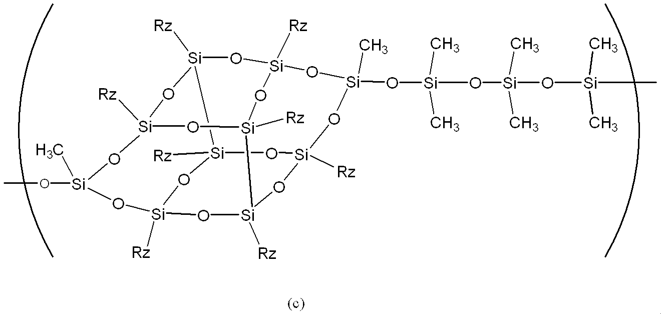
なお、式(a)の複数のRx、式(b)の複数のRy、及び式(c)の複数のRzは、それぞれ同一でも相異なっていてもよい。 Among these, as Rx, Ry, and Rz, a hydrogen atom, an alkyl group having 1 to 6 carbon atoms, or a phenyl group is preferable, and an alkyl group having 1 to 6 carbon atoms is particularly preferable.
Note that the plurality of Rx in the formula (a), the plurality of Ry in the formula (b), and the plurality of Rz in the formula (c) may be the same or different.
例えば、ポリオルガノシロキサン系化合物を含む層は、ポリオルガノシロキサン系化合物の少なくとも一種、所望により他の成分、及び溶剤等を含有する層形成用溶液を、適当な基材の上に塗布し、得られた塗膜を乾燥し、必要に応じて加熱等して形成することができる。基材は、後述する他の層の素材からなるフィルムを用いることができる。 There is no restriction | limiting in particular as a method of forming a polymer layer.
For example, a layer containing a polyorganosiloxane compound is obtained by applying a layer forming solution containing at least one polyorganosiloxane compound, optionally other components, and a solvent on a suitable substrate. The obtained coating film can be dried and formed by heating or the like as necessary. As the substrate, a film made of a material of another layer described later can be used.
また、高分子層として、前記高分子からなる市販の高分子フィルムを用いることもできる。 The thickness of the layer containing the polyorganosiloxane compound to be formed is not particularly limited, but is usually 30 nm to 100 μm.
In addition, as the polymer layer, a commercially available polymer film made of the polymer can be used.
有機ケイ素化合物としては、テトラメトキシシラン、テトラエトキシシラン、テトラn-プロポキシシラン、テトライソプロポキシシラン、テトラn-ブトキシシラン、テトラt-ブトキシシラン等のテトラアルコキシシラン;
ジメチルジメトキシシラン、ジメチルジエトキシシラン、ジエチルジメトキシシラン、メチルトリエトキシシラン、エチルトリメトキシシラン、(3,3,3-トリフルオロプロピル)トリメトキシシラン等の無置換若しくは置換基を有するアルキルアルコキシシラン;
ジフェニルジメトキシシラン、フェニルトリエトキシシラン等のアリールアルコキシシラン;
ヘキサメチルジシロキサン(HMDSO)等のジシロキサン;
ビス(ジメチルアミノ)ジメチルシラン、ビス(ジメチルアミノ)メチルビニルシラン、ビス(エチルアミノ)ジメチルシラン、ジエチルアミノトリメチルシラン、ジメチルアミノジメチルシラン、テトラキスジメチルアミノシラン、トリス(ジメチルアミノ)シラン等のアミノシラン;
ヘキサメチルジシラザン、ヘキサメチルシクロトリシラザン、ヘプタメチルジシラザン、ノナメチルトリシラザン、オクタメチルシクロテトラシラザン、テトラメチルジシラザン等のシラザン;
テトライソシアナートシラン等のシアナートシラン;
トリエトキシフルオロシラン等のハロゲノシラン;
ジアリルジメチルシラン、アリルトリメチルシラン等のアルケニルシラン;
ジ-t-ブチルシラン、1,3-ジシラブタン、ビス(トリメチルシリル)メタン、トリメチルシラン、テトラメチルシラン、トリス(トリメチルシリル)メタン、トリス(トリメチルシリル)シラン、ベンジルトリメチルシラン等の無置換若しくは置換基を有するアルキルシラン;
ビス(トリメチルシリル)アセチレン、トリメチルシリルアセチレン、1-(トリメチルシリル)-1-プロピン等のシリルアルキン;
1,4-ビストリメチルシリル-1,3-ブタジイン、シクロペンタジエニルトリメチルシラン等のシリルアルケン;
フェニルジメチルシラン、フェニルトリメチルシラン等のアリールアルキルシラン;
プロパルギルトリメチルシラン等のアルキニルアルキルシラン;
ビニルトリメチルシラン等のアルケニルアルキルシラン;
ヘキサメチルジシラン等のジシラン;
オクタメチルシクロテトラシロキサン、テトラメチルシクロテトラシロキサン、ヘキサメチルシクロテトラシロキサン等のシロキサン;
N,O-ビス(トリメチルシリル)アセトアミド;
ビス(トリメチルシリル)カルボジイミド;
等が挙げられる。これらのガスは、一種単独で、あるいは二種以上を組み合わせて用いてもよい。 Examples of the silicon compound include silane (SiH 4 ) and organosilicon compounds.
Examples of the organosilicon compound include tetraalkoxysilanes such as tetramethoxysilane, tetraethoxysilane, tetra n-propoxysilane, tetraisopropoxysilane, tetra n-butoxysilane, and tetra t-butoxysilane;
An alkylalkoxysilane having an unsubstituted or substituted group such as dimethyldimethoxysilane, dimethyldiethoxysilane, diethyldimethoxysilane, methyltriethoxysilane, ethyltrimethoxysilane, (3,3,3-trifluoropropyl) trimethoxysilane;
Arylalkoxysilanes such as diphenyldimethoxysilane and phenyltriethoxysilane;
Disiloxanes such as hexamethyldisiloxane (HMDSO);
Aminosilanes such as bis (dimethylamino) dimethylsilane, bis (dimethylamino) methylvinylsilane, bis (ethylamino) dimethylsilane, diethylaminotrimethylsilane, dimethylaminodimethylsilane, tetrakisdimethylaminosilane, tris (dimethylamino) silane;
Silazanes such as hexamethyldisilazane, hexamethylcyclotrisilazane, heptamethyldisilazane, nonamethyltrisilazane, octamethylcyclotetrasilazane, tetramethyldisilazane;
Cyanate silanes such as tetraisocyanate silane;
Halogenosilanes such as triethoxyfluorosilane;
Alkenylsilanes such as diallyldimethylsilane and allyltrimethylsilane;
Unsubstituted or substituted alkyl such as di-t-butylsilane, 1,3-disilabutane, bis (trimethylsilyl) methane, trimethylsilane, tetramethylsilane, tris (trimethylsilyl) methane, tris (trimethylsilyl) silane, benzyltrimethylsilane Silane;
Silylalkynes such as bis (trimethylsilyl) acetylene, trimethylsilylacetylene, 1- (trimethylsilyl) -1-propyne;
Silylalkenes such as 1,4-bistrimethylsilyl-1,3-butadiyne, cyclopentadienyltrimethylsilane;
Arylalkylsilanes such as phenyldimethylsilane and phenyltrimethylsilane;
Alkynylalkylsilanes such as propargyltrimethylsilane;
Alkenylalkylsilanes such as vinyltrimethylsilane;
Disilanes such as hexamethyldisilane;
Siloxanes such as octamethylcyclotetrasiloxane, tetramethylcyclotetrasiloxane, hexamethylcyclotetrasiloxane;
N, O-bis (trimethylsilyl) acetamide;
Bis (trimethylsilyl) carbodiimide;
Etc. These gases may be used alone or in combination of two or more.
ポリアミドとしては、全芳香族ポリアミド、ナイロン6、ナイロン66、ナイロン共重合体等が挙げられる。 Examples of the polyester include polyethylene terephthalate, polybutylene terephthalate, polyethylene naphthalate, and polyarylate.
Examples of the polyamide include wholly aromatic polyamide, nylon 6, nylon 66, nylon copolymer, and the like.
本発明の成形体の製造方法は、高分子層を表面部に有する成形物の、前記高分子層の表面部に、ケイ素化合物のイオンを注入する工程を有することを特徴とする。 2) Manufacturing method of molded object The manufacturing method of the molded object of this invention has the process of inject | pouring the ion of a silicon compound into the surface part of the said polymer layer of the molding which has a polymer layer in a surface part. Features.
この製造方法によれば、例えば、長尺の成形物を巻き出しロールから巻き出し、それを一定方向に搬送しながらイオンを注入し、巻き取りロールで巻き取ることができるので、イオンが注入されて得られる成形体を連続的に製造することができる。 In the method for producing a molded article of the present invention, a molded article is produced by injecting ions of a silicon compound into a polymer layer while conveying a long molded article having a polymer layer on the surface portion in a certain direction. Is preferred.
According to this manufacturing method, for example, a long molded product can be unwound from an unwinding roll, and ions can be injected while being conveyed in a certain direction, and can be wound up by a winding roll. The molded product obtained in this way can be continuously produced.
プラズマイオン注入装置としては、具体的には、(α)高分子層(以下、「イオン注入する層」ということがある。)に負の高電圧パルスを印加するフィードスルーに高周波電力を重畳してイオン注入する層の周囲を均等にプラズマで囲み、プラズマ中のイオンを誘引、注入、衝突、堆積させる装置(特開2001-26887号公報)、(β)チャンバー内にアンテナを設け、高周波電力を与えてプラズマを発生させてイオン注入する層周囲にプラズマが到達後、イオン注入する層に正と負のパルスを交互に印加することで、正のパルスでプラズマ中の電子を誘引衝突させてイオン注入する層を加熱し、パルス定数を制御して温度制御を行いつつ、負のパルスを印加してプラズマ中のイオンを誘引、注入させる装置(特開2001-156013号公報)、(γ)マイクロ波等の高周波電力源等の外部電界を用いてプラズマを発生させ、高電圧パルスを印加してプラズマ中のイオンを誘引、注入させるプラズマイオン注入装置、(δ)外部電界を用いることなく高電圧パルスの印加により発生する電界のみで発生するプラズマ中のイオンを注入するプラズマイオン注入装置等が挙げられる。 When ions in plasma are implanted into the surface portion of the layer, a plasma ion implantation apparatus is used.
Specifically, as a plasma ion implantation apparatus, (α) a high-frequency power is superimposed on a feedthrough that applies a negative high-voltage pulse to a polymer layer (hereinafter also referred to as “ion-implanted layer”). A device that uniformly surrounds the periphery of the ion-implanted layer with plasma and attracts, implants, collides and deposits ions in the plasma (Japanese Patent Laid-Open No. 2001-26887), (β) An antenna is provided in the chamber, and a high-frequency power After the plasma reaches the periphery of the layer to be ion-implanted by applying plasma, positive and negative pulses are alternately applied to the layer to be ion-implanted, so that the electrons in the plasma are attracted and collided with the positive pulse. An apparatus for heating a layer to be ion-implanted and controlling the pulse constant to control the temperature while applying a negative pulse to attract and implant ions in the plasma (Japanese Patent Laid-Open No. 2001-1560) 13), (γ) a plasma ion implantation apparatus that generates plasma using an external electric field such as a high-frequency power source such as a microwave and applies high voltage pulses to attract and inject ions in the plasma, (δ And a plasma ion implantation apparatus that implants ions in plasma generated only by an electric field generated by applying a high voltage pulse without using an external electric field.
以下、前記(γ)及び(δ)のプラズマイオン注入装置を用いる方法について、図面を参照しながら詳細に説明する。 Among these, it is preferable to use the plasma ion implantation apparatus (γ) or (δ) because the processing operation is simple, the processing time can be greatly shortened, and it is suitable for continuous use.
Hereinafter, a method using the plasma ion implantation apparatuses (γ) and (δ) will be described in detail with reference to the drawings.
図1(a)において、1aはイオン注入される高分子層を表面部に有する長尺のフィルム状の成形物(以下、「フィルム」という。)、11aはチャンバー、20aはターボ分子ポンプ、3aはイオン注入される前のフィルム1aを送り出す巻き出しロール、5aはイオン注入されたフィルム(成形体)1bをロール状に巻き取る巻取りロール、2aは高電圧印加回転キャン、6aはフィルムの送り出しロール、10aはガス導入口、7aは高電圧パルス電源、4はプラズマ放電用電極(外部電界)である。図1(b)は、前記高電圧印加回転キャン2aの斜視図であり、15は高電圧導入端子(フィードスルー)である。 FIG. 1 is a diagram showing an outline of a continuous plasma ion implantation apparatus including the plasma ion implantation apparatus (γ).
In FIG. 1A, 1a is a long film-like molded product (hereinafter referred to as “film”) having a polymer layer to be ion-implanted on its surface, 11a is a chamber, 20a is a turbo molecular pump, 3a. Is an unwinding roll for feeding out the
本発明の電子デバイス用部材は、本発明の成形体からなることを特徴とする。従って、本発明の電子デバイス用部材は、優れたガスバリア性を有しているので、水蒸気等のガスによる素子の劣化を防ぐことができる。また、液晶ディスプレイ、ELディスプレイ等のディスプレイ部材;太陽電池用保護シート(バックシート)等の太陽電池用部材;等として好適である。 3) Electronic device member and electronic device The electronic device member of the present invention is characterized by comprising the molded article of the present invention. Therefore, since the electronic device member of the present invention has excellent gas barrier properties, it is possible to prevent deterioration of the element due to gas such as water vapor. Moreover, it is suitable as display members, such as a liquid crystal display and an EL display; Solar cell members, such as a solar cell protective sheet (back sheet);
本発明の電子デバイスは、本発明の成形体からなる電子デバイス用部材を備えているので、ガスバリア性、及び耐屈曲性に優れる。 The electronic device of the present invention includes the electronic device member of the present invention. Specific examples include a liquid crystal display, an organic EL display, an inorganic EL display, electronic paper, and a solar battery.
Since the electronic device of the present invention includes the electronic device member comprising the molded article of the present invention, the electronic device is excellent in gas barrier properties and bending resistance.
RF電源:型番号「RF」56000、日本電子社製
高電圧パルス電源:「PV-3-HSHV-0835」、栗田製作所社製
(水蒸気透過率測定装置)
透過率測定器:「L89-500」、LYSSY社製
測定条件:相対湿度90%、40℃ (Plasma ion implantation system)
RF power source: Model number “RF” 56000, JEOL high voltage pulse power source: “PV-3-HSHV-0835”, Kurita Manufacturing Co., Ltd. (water vapor transmission rate measuring device)
Transmittance measuring instrument: “L89-500”, manufactured by LYSSY, Inc. Measurement conditions: relative humidity 90%, 40 ° C.
原子間力顕微鏡(AFM)(「SPA300 HV」、エスアイアイ・ナノテクノロジー社製)を用いて測定領域1×1μm(1μm□)及び25×25μm(25μm□)における表面粗さRa値(nm)を測定した。 (Surface smoothness evaluation method)
Using an atomic force microscope (AFM) ("SPA300 HV", manufactured by SII Nanotechnology), surface roughness Ra value (nm) in a measurement region of 1 × 1 μm (1 μm □) and 25 × 25 μm (25 μm □) Was measured.
3mmφステンレスの棒に、得られた成形体のイオン注入面(比較例1はポリジメチルシロキサン側、比較例2は窒化ケイ素膜側)を外側にして成形体を巻きつけ、周方向に10往復させた後、光学顕微鏡(倍率2000倍、キーエンス社製)でクラック発生の有無を観察した。クラックの発生が認められなかった場合を「なし」、クラックの発生が認められた場合を「あり」と評価した。 (Bend resistance test)
The molded body was wound around a 3 mmφ stainless steel rod with the ion-implanted surface (Comparative Example 1 on the polydimethylsiloxane side and Comparative Example 2 on the silicon nitride film side) of the obtained molded body on the outside, and was reciprocated 10 times in the circumferential direction. Thereafter, the occurrence of cracks was observed with an optical microscope (magnification 2000 times, manufactured by Keyence Corporation). The case where crack generation was not recognized was evaluated as “none”, and the case where crack generation was observed was evaluated as “present”.
基材としてのポリエチレンテレフタレートフィルム(「PET38T-300」、三菱樹脂社製、厚さ38μm)(以下、「PETフィルム」という。)に、シリコーン剥離剤(「BY-24-561」、ポリジメチルシロキサンを主成分とするシリコーン樹脂、信越化学工業社製)を塗布し、120℃で2分間加熱して、PETフィルム上に厚さ100nmの高分子層(ポリジメチルシロキサンを含む層)を形成して成形物を得た。次に、図1に示すプラズマイオン注入装置を用いてポリジメチルシロキサンを含む層の表面に、イオン注入ガス(プラズマ生成ガス)としてヘキサメチルジシロキサン(HMDSO)のガスをプラズマイオン注入して成形体1を作製した。 Example 1
Polyethylene terephthalate film (“PET38T-300”, manufactured by Mitsubishi Plastics Co., Ltd., thickness 38 μm) (hereinafter referred to as “PET film”) as a base material, silicone release agent (“BY-24-561”, polydimethylsiloxane) A silicone resin (manufactured by Shin-Etsu Chemical Co., Ltd.) is heated and heated at 120 ° C. for 2 minutes to form a polymer layer (a layer containing polydimethylsiloxane) having a thickness of 100 nm on the PET film. A molded product was obtained. Next, using a plasma ion implantation apparatus shown in FIG. 1, hexamethyldisiloxane (HMDSO) gas is ion-implanted as an ion implantation gas (plasma generating gas) onto the surface of the layer containing polydimethylsiloxane, and a compact is formed. 1 was produced.
・Duty比:0.5%
・繰り返し周波数:1000Hz
・印加電圧:-10kV
・RF電源:周波 13.56MHz、印加電力 1000W
・チャンバー内圧:0.2Pa
・パルス幅:5μsec
・処理時間(イオン注入時間):5分間
・ガス流量:40ccm The conditions for plasma ion implantation are shown below.
・ Duty ratio: 0.5%
・ Repetition frequency: 1000Hz
・ Applied voltage: -10kV
・ RF power supply: frequency 13.56 MHz, applied power 1000 W
-Chamber internal pressure: 0.2 Pa
・ Pulse width: 5μsec
・ Processing time (ion implantation time): 5 minutes ・ Gas flow rate: 40 ccm
プラズマ生成ガスとして、HMDSOの代わりにトリメチルシランを用いた以外は、実施例1と同様にして成形体2を作製した。 (Example 2)
A molded body 2 was produced in the same manner as in Example 1 except that trimethylsilane was used instead of HMDSO as the plasma generating gas.
プラズマ生成ガスとして、HMDSOの代わりにテトラエトキシシランを用いた以外は、実施例1と同様にして成形体3を作製した。 (Example 3)
A molded body 3 was produced in the same manner as in Example 1 except that tetraethoxysilane was used instead of HMDSO as the plasma generating gas.
PETフィルムにシリコーン剥離剤を塗布しない以外は、実施例1と同様にして成形体を作製した。すなわち、PETフィルムの表面に直接HMDSOをプラズマイオン注入して成形体4とした。 Example 4
A molded body was produced in the same manner as in Example 1 except that the silicone release agent was not applied to the PET film. That is, HMDSO was directly ion-implanted into the surface of the PET film to obtain a molded body 4.
イオン注入を行わない以外は、実施例1と同様にして成形体を作製した。すなわち、PETフィルム上にポリジメチルシロキサンを含む層を形成し、成形体5とした。
(比較例2)
PETフィルムに、スパッタリング法により、厚さ50nmの窒化ケイ素(Si3N4)の膜を設け、成形体6を作製した。 (Comparative Example 1)
A molded body was produced in the same manner as in Example 1 except that ion implantation was not performed. That is, a layer containing polydimethylsiloxane was formed on the PET film to obtain a molded body 5.
(Comparative Example 2)
A film of silicon nitride (Si 3 N 4 ) having a thickness of 50 nm was provided on the PET film by a sputtering method to produce a molded body 6.

さらに、実施例1~4の成形体は、比較例1、2の成形体に比して、表面平滑性に優れていた。
以上のことから、高分子層にケイ素化合物のイオン注入を適切な条件で行うことにより、ガスバリア性、耐屈曲性及び表面平滑性に優れた成形体が得られることがわかる。 From Table 1, the molded bodies 1 to 4 of Examples 1 to 4 had a lower water vapor transmission rate than the molded bodies 5 and 6 of Comparative Examples 1 and 2. Further, no cracks were observed in the bending resistance test. In the molded body 6 of Comparative Example 2, cracks occurred in the silicon nitride film.
Furthermore, the molded bodies of Examples 1 to 4 were excellent in surface smoothness as compared with the molded bodies of Comparative Examples 1 and 2.
From the above, it can be seen that a molded body excellent in gas barrier properties, flex resistance and surface smoothness can be obtained by performing ion implantation of a silicon compound into a polymer layer under appropriate conditions.
Claims (10)
- 高分子層にケイ素化合物のイオンが注入されて得られるイオン注入層を有することを特徴とする成形体。 A molded product comprising an ion-implanted layer obtained by implanting silicon compound ions into a polymer layer.
- 高分子層に、プラズマイオン注入法により、ケイ素化合物のイオンが注入されて得られるイオン注入層を有することを特徴とする請求項1に記載の成形体。 The molded article according to claim 1, further comprising an ion-implanted layer obtained by implanting silicon compound ions into the polymer layer by a plasma ion implantation method.
- 前記高分子層が、ポリオルガノシロキサン系化合物を含む層であることを特徴とする請求項1又は2に記載の成形体。 The molded body according to claim 1 or 2, wherein the polymer layer is a layer containing a polyorganosiloxane compound.
- 40℃、相対湿度90%雰囲気下での水蒸気透過率が1g/m2/day未満であることを特徴とする請求項1~3のいずれかに記載の成形体。 The molded article according to any one of claims 1 to 3, which has a water vapor permeability of less than 1 g / m 2 / day in an atmosphere of 40 ° C and a relative humidity of 90%.
- 高分子層を表面部に有する成形物の、前記高分子層の表面部に、ケイ素化合物のイオンを注入する工程を有する請求項1に記載の成形体の製造方法。 The method for producing a molded article according to claim 1, further comprising a step of injecting silicon compound ions into the surface portion of the polymer layer of the molded product having the polymer layer on the surface portion.
- 高分子層を表面部に有する成形物の、前記高分子層の表面部に、プラズマイオン注入法によりケイ素化合物のイオンを注入する工程を有する請求項2に記載の成形体の製造方法。 The method for producing a molded article according to claim 2, further comprising a step of implanting silicon compound ions into the surface portion of the polymer layer by a plasma ion implantation method.
- 高分子層を表面部に有する長尺の成形物を一定方向に搬送しながら、前記高分子層に、ケイ素化合物のイオンを注入することを特徴とする請求項5又は6に記載の成形体の製造方法。 7. The molded product according to claim 5, wherein ions of a silicon compound are implanted into the polymer layer while conveying a long molded product having a polymer layer on a surface portion in a certain direction. Production method.
- 前記高分子層が、ポリオルガノシロキサン系化合物を含む層であることを特徴とする請求項5~7のいずれかに記載の成形体の製造方法。 The method for producing a molded body according to any one of claims 5 to 7, wherein the polymer layer is a layer containing a polyorganosiloxane compound.
- 請求項1~4のいずれかに記載の成形体からなる電子デバイス用部材。 An electronic device member comprising the molded article according to any one of claims 1 to 4.
- 請求項8に記載の電子デバイス用部材を備える電子デバイス。 An electronic device comprising the electronic device member according to claim 8.
Priority Applications (4)
| Application Number | Priority Date | Filing Date | Title |
|---|---|---|---|
| US13/256,143 US8865810B2 (en) | 2009-03-26 | 2010-03-24 | Formed article, method for producing same, electronic device member, and electronic device |
| CN201080015641.4A CN102388160B (en) | 2009-03-26 | 2010-03-24 | Molded body, method for producing same, electronic device member, and electronic device |
| EP10756100.3A EP2412845A4 (en) | 2009-03-26 | 2010-03-24 | Molded body, method for producing same, electronic device member, and electronic device |
| KR1020147031582A KR101515771B1 (en) | 2009-03-26 | 2010-03-24 | Molded body, method for producing same, electronic device member, and electronic device |
Applications Claiming Priority (2)
| Application Number | Priority Date | Filing Date | Title |
|---|---|---|---|
| JP2009076028A JP5379530B2 (en) | 2009-03-26 | 2009-03-26 | Molded body, manufacturing method thereof, electronic device member and electronic device |
| JP2009-076028 | 2009-03-26 |
Publications (1)
| Publication Number | Publication Date |
|---|---|
| WO2010110304A1 true WO2010110304A1 (en) | 2010-09-30 |
Family
ID=42780998
Family Applications (1)
| Application Number | Title | Priority Date | Filing Date |
|---|---|---|---|
| PCT/JP2010/055064 WO2010110304A1 (en) | 2009-03-26 | 2010-03-24 | Molded body, method for producing same, electronic device member, and electronic device |
Country Status (7)
| Country | Link |
|---|---|
| US (1) | US8865810B2 (en) |
| EP (1) | EP2412845A4 (en) |
| JP (1) | JP5379530B2 (en) |
| KR (2) | KR101515771B1 (en) |
| CN (1) | CN102388160B (en) |
| TW (1) | TWI490258B (en) |
| WO (1) | WO2010110304A1 (en) |
Cited By (2)
| Publication number | Priority date | Publication date | Assignee | Title |
|---|---|---|---|---|
| US20140072798A1 (en) * | 2011-03-30 | 2014-03-13 | Lintec Corporation | Gas barrier laminated body, method for producing same, member for electronic device, and electronic device |
| US20140308494A1 (en) * | 2011-11-04 | 2014-10-16 | Lintec Corporation | Gas barrier film, method for producing same, gas barrier film laminate, member for electronic devices, and electronic device |
Families Citing this family (5)
| Publication number | Priority date | Publication date | Assignee | Title |
|---|---|---|---|---|
| JP6225025B2 (en) | 2011-08-03 | 2017-11-01 | リンテック株式会社 | Gas barrier pressure-sensitive adhesive sheet, method for producing the same, electronic member, and optical member |
| WO2013081003A1 (en) | 2011-11-30 | 2013-06-06 | リンテック株式会社 | Manufacturing method for gas barrier film, and electronic member or optical member provided with gas barrier film |
| KR102059326B1 (en) | 2012-03-29 | 2019-12-26 | 린텍 가부시키가이샤 | Gas barrier laminate, method for producing same, member for electronic devices, and electronic device |
| JP6045265B2 (en) * | 2012-09-18 | 2016-12-14 | リンテック株式会社 | Ion implanter |
| CN113226746B (en) | 2018-12-27 | 2023-08-11 | 琳得科株式会社 | Gas barrier laminate |
Citations (6)
| Publication number | Priority date | Publication date | Assignee | Title |
|---|---|---|---|---|
| JP2004530790A (en) * | 2000-11-30 | 2004-10-07 | インターナショナル・ビジネス・マシーンズ・コーポレーション | Method of forming alignment layer surface |
| JP2006052376A (en) * | 2004-02-27 | 2006-02-23 | Lintec Corp | Method for producing polymer molded product, polymer molded product and apparatus for producing the same |
| JP2008174792A (en) * | 2007-01-18 | 2008-07-31 | Plasma Ion Assist Co Ltd | Hydrophilizing modification method for fluorine base synthetic resin, and article obtained thereby |
| JP2008246893A (en) * | 2007-03-30 | 2008-10-16 | Lintec Corp | Highly smooth gas barrier film and its manufacturing method |
| JP2008270115A (en) * | 2007-04-25 | 2008-11-06 | Toppan Printing Co Ltd | Transparent conductive gas barrier film |
| WO2010021326A1 (en) * | 2008-08-19 | 2010-02-25 | リンテック株式会社 | Moulded article, method for producing the same, electronic device member, and electronic device |
Family Cites Families (88)
| Publication number | Priority date | Publication date | Assignee | Title |
|---|---|---|---|---|
| US4557946A (en) * | 1983-06-03 | 1985-12-10 | Edward Sacher | Moisture impermeability or organosilicone films |
| US4842941A (en) | 1987-04-06 | 1989-06-27 | General Electric Company | Method for forming abrasion-resistant polycarbonate articles, and articles of manufacture produced thereby |
| US5143747A (en) | 1991-02-12 | 1992-09-01 | Hughes Aircraft Company | Die improved tooling for metal working |
| JPH05185568A (en) | 1992-01-14 | 1993-07-27 | Diafoil Co Ltd | Film for liquid crystal display panel |
| DE69305794T2 (en) | 1992-07-10 | 1997-06-12 | Asahi Glass Co Ltd | Transparent, conductive film and target and material for vapor deposition for its manufacture |
| JPH0664105A (en) | 1992-08-12 | 1994-03-08 | Mitsui Toatsu Chem Inc | Gas barrier transparent conductive laminate |
| JP3453805B2 (en) | 1992-09-11 | 2003-10-06 | 旭硝子株式会社 | Transparent conductive film |
| JPH0845452A (en) | 1994-08-01 | 1996-02-16 | Takamisawa Denki Seisakusho:Kk | Ion balance measuring device and measuring method for the balance |
| JP3515255B2 (en) | 1994-12-20 | 2004-04-05 | 株式会社東芝 | Transparent conductive substrate, method for manufacturing transparent conductive substrate, and display device |
| US5907382A (en) | 1994-12-20 | 1999-05-25 | Kabushiki Kaisha Toshiba | Transparent conductive substrate and display apparatus |
| JP3484550B2 (en) | 1994-12-22 | 2004-01-06 | 大日本印刷株式会社 | Retort packaging film |
| JPH0910687A (en) | 1995-03-31 | 1997-01-14 | Tonen Corp | Production of silicon dioxide based ceramic coating film |
| JP3489269B2 (en) | 1995-04-28 | 2004-01-19 | 東洋製罐株式会社 | Gas barrier transparent packaging material and method for producing the same |
| JP3562065B2 (en) | 1995-10-30 | 2004-09-08 | 日新電機株式会社 | High gas barrier polymer article and method for producing the same |
| JP4144042B2 (en) | 1997-03-06 | 2008-09-03 | 東洋製罐株式会社 | Gas barrier plastic packaging material and manufacturing method thereof |
| JP4019334B2 (en) | 1997-03-07 | 2007-12-12 | 東レ株式会社 | Polyester film for gas barrier |
| JP3951348B2 (en) | 1997-03-14 | 2007-08-01 | 東洋製罐株式会社 | Laminate with excellent gas barrier properties and flexibility |
| JP3484094B2 (en) | 1999-02-26 | 2004-01-06 | グンゼ株式会社 | Silica-coated plastic film and method for producing the same |
| JP4205241B2 (en) | 1999-03-04 | 2009-01-07 | 住友化学株式会社 | Laminated body |
| US20060017162A1 (en) | 1999-03-12 | 2006-01-26 | Shoji Seta | Semiconductor device and manufacturing method of the same |
| JP4270632B2 (en) | 1999-03-12 | 2009-06-03 | 株式会社東芝 | Manufacturing method of semiconductor device using dry etching |
| US6849923B2 (en) | 1999-03-12 | 2005-02-01 | Kabushiki Kaisha Toshiba | Semiconductor device and manufacturing method of the same |
| JP2000338901A (en) | 1999-06-01 | 2000-12-08 | Matsushita Electric Ind Co Ltd | Manufacture of flexible display substrate |
| JP2001119051A (en) | 1999-10-19 | 2001-04-27 | Dainippon Printing Co Ltd | Rear-surface protecting sheet for solar cell module and solar cell module using the same |
| JP2001207259A (en) | 2000-01-25 | 2001-07-31 | Natl Inst Of Advanced Industrial Science & Technology Meti | Surface modification method and system |
| US6416817B1 (en) | 2000-03-03 | 2002-07-09 | Dow Corning Sa | Barrier coatings having bis-silanes |
| JP2002018246A (en) | 2000-07-07 | 2002-01-22 | Sony Corp | Barrier film |
| JP5291275B2 (en) | 2000-07-27 | 2013-09-18 | 有限会社コンタミネーション・コントロール・サービス | Member provided with coating film and method for producing coating film |
| GB0113751D0 (en) | 2001-06-06 | 2001-07-25 | Dow Corning | Surface treatment |
| JP4669631B2 (en) | 2001-06-18 | 2011-04-13 | 矢崎総業株式会社 | Printed circuit and flexible wiring patterning method |
| JP2003154596A (en) | 2001-11-22 | 2003-05-27 | Nitto Denko Corp | Transparent gas-barrier film, transparent conductive electrode base material, display element, solar cell, or face-shaped emitter using the film |
| US20030228475A1 (en) | 2002-04-18 | 2003-12-11 | Minoru Komada | Barrier film and laminated material, container for wrapping and image display medium using the same, and manufacturing method for barrier film |
| JP2003347570A (en) | 2002-05-27 | 2003-12-05 | Mitsubishi Plastics Ind Ltd | Protective sheet for back side of solar battery |
| US7015640B2 (en) | 2002-09-11 | 2006-03-21 | General Electric Company | Diffusion barrier coatings having graded compositions and devices incorporating the same |
| US7449246B2 (en) | 2004-06-30 | 2008-11-11 | General Electric Company | Barrier coatings |
| JP4185341B2 (en) | 2002-09-25 | 2008-11-26 | パイオニア株式会社 | Multilayer barrier film structure, organic electroluminescence display panel, and manufacturing method |
| JP2004322489A (en) | 2003-04-25 | 2004-11-18 | Pioneer Electronic Corp | Gas-barrier substrate and its production method |
| JP2004352966A (en) | 2003-05-28 | 2004-12-16 | Dengiken:Kk | Electrical/electronic insulating sheet |
| JP2005088431A (en) | 2003-09-18 | 2005-04-07 | Dainippon Printing Co Ltd | Barrier film |
| JP2005104025A (en) | 2003-09-30 | 2005-04-21 | Fuji Photo Film Co Ltd | Laminated film with gas barrier properties and image display element using this laminated film |
| US7635525B2 (en) | 2003-09-30 | 2009-12-22 | Fujifilm Corporation | Gas barrier laminate film and method for producing the same |
| JP2005119160A (en) | 2003-10-17 | 2005-05-12 | Dainippon Printing Co Ltd | Gas barrier film and its manufacturing method |
| JP2005119155A (en) | 2003-10-17 | 2005-05-12 | Dainippon Printing Co Ltd | Gas barrier film and its manufacturing method |
| CA2543666A1 (en) | 2003-10-31 | 2005-05-12 | Ventracor Limited | Plasma immersion ion implantation using conductive mesh |
| JP4531380B2 (en) | 2003-12-15 | 2010-08-25 | 大日本印刷株式会社 | Gas barrier sheet |
| JP4852822B2 (en) | 2004-02-17 | 2012-01-11 | 大日本印刷株式会社 | Barrier film and laminated material using the same |
| JP4494824B2 (en) | 2004-02-24 | 2010-06-30 | 株式会社クラレ | Method for producing film for display device |
| JP5039907B2 (en) | 2004-03-09 | 2012-10-03 | エグザテック・リミテッド・ライアビリティー・カンパニー | Plasma coating apparatus for nonplanar substrates. |
| KR101173713B1 (en) | 2004-04-28 | 2012-08-13 | 니폰 제온 가부시키가이샤 | Multilayer body, light-emitting device and use thereof |
| US20050287307A1 (en) | 2004-06-23 | 2005-12-29 | Varian Semiconductor Equipment Associates, Inc. | Etch and deposition control for plasma implantation |
| US20090110892A1 (en) | 2004-06-30 | 2009-04-30 | General Electric Company | System and method for making a graded barrier coating |
| JP2006035737A (en) | 2004-07-29 | 2006-02-09 | Teijin Ltd | Gas barrier polymer laminated film suitable for display |
| JP2006070238A (en) | 2004-08-05 | 2006-03-16 | Lintec Corp | Method for continuous surface modification of polymer film, apparatus for continuous surface modification and polymer film in which ion injection layer is formed |
| JP2006123306A (en) | 2004-10-28 | 2006-05-18 | Dainippon Printing Co Ltd | Gas barrier laminate |
| JP2006123307A (en) | 2004-10-28 | 2006-05-18 | Dainippon Printing Co Ltd | Gas barrier laminate |
| US20080096014A1 (en) | 2004-12-13 | 2008-04-24 | University Of South Australia | Craze Resistant Plastic Article and Method of Production |
| EP1852522B1 (en) | 2005-02-22 | 2013-04-24 | Toyo Seikan Kaisha, Ltd. | Vapor deposited film by plasma cvd method |
| JP4624152B2 (en) | 2005-03-24 | 2011-02-02 | 富士フイルム株式会社 | Plastic film, gas barrier film, and image display element using the same |
| JP2007022075A (en) | 2005-06-14 | 2007-02-01 | Asahi Kasei Corp | Layer structure and its manufacturing method |
| JP2007042616A (en) | 2005-06-29 | 2007-02-15 | Asahi Kasei Corp | Light emitting element, display device and manufacturing method thereof |
| JP2007065644A (en) | 2005-08-03 | 2007-03-15 | Asahi Kasei Corp | Substrate for display, display and manufacturing method of them |
| JP4099724B2 (en) | 2005-08-09 | 2008-06-11 | 博夫 井上 | bracelet |
| US20090139564A1 (en) | 2005-09-30 | 2009-06-04 | Toray Industries , Inc., A Corporation | Sealing Film for Photovoltaic Cell Module and Photovoltaic Module |
| US20090130463A1 (en) | 2005-10-05 | 2009-05-21 | John Dean Albaugh | Coated Substrates and Methods for their Preparation |
| JP2007237588A (en) | 2006-03-09 | 2007-09-20 | Kyodo Printing Co Ltd | Gas-barrier film and method for producing the film |
| JP2007283726A (en) | 2006-04-20 | 2007-11-01 | Bridgestone Corp | Shaped article and manufacturing method for the same |
| JP2008015500A (en) | 2006-06-09 | 2008-01-24 | Fujifilm Corp | Protection film for polarizing plate |
| JP4725735B2 (en) | 2006-08-25 | 2011-07-13 | Jsr株式会社 | Method for producing silica film laminated film for gas barrier |
| JP4830733B2 (en) | 2006-09-07 | 2011-12-07 | 凸版印刷株式会社 | Gas barrier film and manufacturing method thereof |
| JP2008096617A (en) | 2006-10-11 | 2008-04-24 | Canon Inc | Image forming apparatus |
| JPWO2008096616A1 (en) | 2007-02-05 | 2010-05-20 | コニカミノルタホールディングス株式会社 | Transparent gas barrier film and method for producing the same |
| JPWO2008096617A1 (en) | 2007-02-06 | 2010-05-20 | コニカミノルタホールディングス株式会社 | Transparent gas barrier film and method for producing transparent gas barrier film |
| JP2008204683A (en) | 2007-02-19 | 2008-09-04 | Toppan Printing Co Ltd | Transparent conductive film |
| JP2008235165A (en) | 2007-03-23 | 2008-10-02 | Konica Minolta Holdings Inc | Method of manufacturing roll-like resin film having transparent conductive film |
| JP2009110897A (en) | 2007-11-01 | 2009-05-21 | Toray Ind Inc | Transparent conductive film |
| JP4969479B2 (en) | 2008-02-20 | 2012-07-04 | 尾池工業株式会社 | Manufacturing method of substrate with transparent conductive film |
| US8956731B2 (en) | 2008-02-27 | 2015-02-17 | Dai Nippon Printing Co., Ltd. | Gas barrier sheet |
| JP2009252574A (en) | 2008-04-08 | 2009-10-29 | Toyota Industries Corp | El device |
| JP5551885B2 (en) | 2008-05-01 | 2014-07-16 | 日揮触媒化成株式会社 | Method for forming low dielectric constant silica-based coating and low dielectric constant silica-based coating obtained from the method |
| JP5650109B2 (en) | 2008-06-30 | 2015-01-07 | コーロン インダストリーズ インク | Plastic substrate and element including the same |
| JP5305476B2 (en) | 2008-08-29 | 2013-10-02 | 独立行政法人産業技術総合研究所 | Method for producing silicon oxide thin film or silicon oxynitride compound thin film and thin film obtained by this method |
| CN102245379B (en) | 2008-12-12 | 2015-06-24 | 琳得科株式会社 | Laminate, method for producing same, electronic device member, and electronic device |
| KR101526134B1 (en) | 2009-03-17 | 2015-06-04 | 린텍 가부시키가이샤 | Molded article, process for producing the molded article, member for electronic device, and electronic device |
| WO2010134611A1 (en) | 2009-05-22 | 2010-11-25 | リンテック株式会社 | Molded object, process for producing same, member for electronic device, and electronic device |
| KR101489551B1 (en) | 2009-05-22 | 2015-02-03 | 린텍 가부시키가이샤 | Molded object, process for producing same, member for electronic device, and electronic device |
| JP5612277B2 (en) | 2009-06-16 | 2014-10-22 | リンテック株式会社 | Gas barrier film and electronic device member |
| CN102811853B (en) | 2010-03-31 | 2015-05-20 | 琳得科株式会社 | Transparent conductive film, method for producing same, and electronic device using transparent conductive film |
| KR101886455B1 (en) | 2010-09-07 | 2018-08-07 | 린텍 가부시키가이샤 | Adhesive sheet and electronic device |
-
2009
- 2009-03-26 JP JP2009076028A patent/JP5379530B2/en active Active
-
2010
- 2010-03-19 TW TW099108132A patent/TWI490258B/en active
- 2010-03-24 WO PCT/JP2010/055064 patent/WO2010110304A1/en active Application Filing
- 2010-03-24 EP EP10756100.3A patent/EP2412845A4/en not_active Withdrawn
- 2010-03-24 CN CN201080015641.4A patent/CN102388160B/en active Active
- 2010-03-24 US US13/256,143 patent/US8865810B2/en active Active
- 2010-03-24 KR KR1020147031582A patent/KR101515771B1/en active IP Right Grant
- 2010-03-24 KR KR1020117022384A patent/KR20120000067A/en active Application Filing
Patent Citations (6)
| Publication number | Priority date | Publication date | Assignee | Title |
|---|---|---|---|---|
| JP2004530790A (en) * | 2000-11-30 | 2004-10-07 | インターナショナル・ビジネス・マシーンズ・コーポレーション | Method of forming alignment layer surface |
| JP2006052376A (en) * | 2004-02-27 | 2006-02-23 | Lintec Corp | Method for producing polymer molded product, polymer molded product and apparatus for producing the same |
| JP2008174792A (en) * | 2007-01-18 | 2008-07-31 | Plasma Ion Assist Co Ltd | Hydrophilizing modification method for fluorine base synthetic resin, and article obtained thereby |
| JP2008246893A (en) * | 2007-03-30 | 2008-10-16 | Lintec Corp | Highly smooth gas barrier film and its manufacturing method |
| JP2008270115A (en) * | 2007-04-25 | 2008-11-06 | Toppan Printing Co Ltd | Transparent conductive gas barrier film |
| WO2010021326A1 (en) * | 2008-08-19 | 2010-02-25 | リンテック株式会社 | Moulded article, method for producing the same, electronic device member, and electronic device |
Non-Patent Citations (1)
| Title |
|---|
| See also references of EP2412845A4 * |
Cited By (3)
| Publication number | Priority date | Publication date | Assignee | Title |
|---|---|---|---|---|
| US20140072798A1 (en) * | 2011-03-30 | 2014-03-13 | Lintec Corporation | Gas barrier laminated body, method for producing same, member for electronic device, and electronic device |
| US9763345B2 (en) * | 2011-03-30 | 2017-09-12 | Lintec Corporation | Gas barrier laminated body, method for producing same, member for electronic device, and electronic device |
| US20140308494A1 (en) * | 2011-11-04 | 2014-10-16 | Lintec Corporation | Gas barrier film, method for producing same, gas barrier film laminate, member for electronic devices, and electronic device |
Also Published As
| Publication number | Publication date |
|---|---|
| KR101515771B1 (en) | 2015-04-28 |
| JP5379530B2 (en) | 2013-12-25 |
| EP2412845A1 (en) | 2012-02-01 |
| US8865810B2 (en) | 2014-10-21 |
| CN102388160B (en) | 2015-06-10 |
| US20120041116A1 (en) | 2012-02-16 |
| KR20140141722A (en) | 2014-12-10 |
| TWI490258B (en) | 2015-07-01 |
| EP2412845A4 (en) | 2014-10-29 |
| KR20120000067A (en) | 2012-01-03 |
| JP2010229445A (en) | 2010-10-14 |
| CN102388160A (en) | 2012-03-21 |
| TW201035211A (en) | 2010-10-01 |
Similar Documents
| Publication | Publication Date | Title |
|---|---|---|
| JP5379530B2 (en) | Molded body, manufacturing method thereof, electronic device member and electronic device | |
| JP5704610B2 (en) | Molded body, manufacturing method thereof, electronic device member and electronic device | |
| JP5612277B2 (en) | Gas barrier film and electronic device member | |
| WO2010021326A1 (en) | Moulded article, method for producing the same, electronic device member, and electronic device | |
| JP5992331B2 (en) | Molded body, manufacturing method thereof, electronic device member and electronic device | |
| KR101489552B1 (en) | Molded object, process for producing same, member for electronic device, and electronic device | |
| JP5631864B2 (en) | Molded body, manufacturing method thereof, member for electronic device, and electronic device | |
| EP2554602B1 (en) | Molded object, process for producing same, member for electronic device, and electronic device | |
| JP5750441B2 (en) | Molded body, manufacturing method thereof, member for electronic device, and electronic device | |
| JP2010284845A (en) | Gas barrier film and method for forming the same | |
| KR101442371B1 (en) | Molded article, method for producing the same, electronic device member, and electronic device |
Legal Events
| Date | Code | Title | Description |
|---|---|---|---|
| WWE | Wipo information: entry into national phase |
Ref document number: 201080015641.4 Country of ref document: CN |
|
| 121 | Ep: the epo has been informed by wipo that ep was designated in this application |
Ref document number: 10756100 Country of ref document: EP Kind code of ref document: A1 |
|
| WWE | Wipo information: entry into national phase |
Ref document number: 2010756100 Country of ref document: EP |
|
| ENP | Entry into the national phase |
Ref document number: 20117022384 Country of ref document: KR Kind code of ref document: A |
|
| NENP | Non-entry into the national phase |
Ref country code: DE |
|
| WWE | Wipo information: entry into national phase |
Ref document number: 13256143 Country of ref document: US |