JP2009252574A - El device - Google Patents
El device Download PDFInfo
- Publication number
- JP2009252574A JP2009252574A JP2008100064A JP2008100064A JP2009252574A JP 2009252574 A JP2009252574 A JP 2009252574A JP 2008100064 A JP2008100064 A JP 2008100064A JP 2008100064 A JP2008100064 A JP 2008100064A JP 2009252574 A JP2009252574 A JP 2009252574A
- Authority
- JP
- Japan
- Prior art keywords
- sealing film
- organic
- polymer
- polysilazane
- coating composition
- Prior art date
- Legal status (The legal status is an assumption and is not a legal conclusion. Google has not performed a legal analysis and makes no representation as to the accuracy of the status listed.)
- Pending
Links
- 238000007789 sealing Methods 0.000 claims abstract description 87
- 229920000642 polymer Polymers 0.000 claims abstract description 68
- 239000002904 solvent Substances 0.000 claims abstract description 64
- 239000008199 coating composition Substances 0.000 claims abstract description 41
- 229920001709 polysilazane Polymers 0.000 claims abstract description 41
- 238000000034 method Methods 0.000 claims abstract description 38
- 125000003808 silyl group Chemical group [H][Si]([H])([H])[*] 0.000 claims abstract description 35
- 239000000758 substrate Substances 0.000 claims abstract description 35
- 229910010272 inorganic material Inorganic materials 0.000 claims abstract description 8
- 239000011147 inorganic material Substances 0.000 claims abstract description 8
- 239000000203 mixture Substances 0.000 claims abstract description 7
- 125000002887 hydroxy group Chemical group [H]O* 0.000 claims description 34
- XEKOWRVHYACXOJ-UHFFFAOYSA-N Ethyl acetate Chemical group CCOC(C)=O XEKOWRVHYACXOJ-UHFFFAOYSA-N 0.000 claims description 18
- 230000001681 protective effect Effects 0.000 claims description 17
- 239000002994 raw material Substances 0.000 claims description 17
- 238000005268 plasma chemical vapour deposition Methods 0.000 claims description 7
- 125000000113 cyclohexyl group Chemical group [H]C1([H])C([H])([H])C([H])([H])C([H])(*)C([H])([H])C1([H])[H] 0.000 claims 1
- VYPSYNLAJGMNEJ-UHFFFAOYSA-N Silicium dioxide Chemical compound O=[Si]=O VYPSYNLAJGMNEJ-UHFFFAOYSA-N 0.000 abstract description 22
- 239000011521 glass Substances 0.000 abstract description 20
- 239000000463 material Substances 0.000 abstract description 15
- 239000000377 silicon dioxide Substances 0.000 abstract description 11
- XLYOFNOQVPJJNP-UHFFFAOYSA-N water Chemical group O XLYOFNOQVPJJNP-UHFFFAOYSA-N 0.000 abstract description 6
- 239000002114 nanocomposite Substances 0.000 abstract description 4
- 239000010408 film Substances 0.000 description 96
- 239000000126 substance Substances 0.000 description 8
- 238000000576 coating method Methods 0.000 description 7
- 239000000178 monomer Substances 0.000 description 7
- 238000000151 deposition Methods 0.000 description 6
- 239000012298 atmosphere Substances 0.000 description 5
- 230000015572 biosynthetic process Effects 0.000 description 5
- 230000008021 deposition Effects 0.000 description 5
- 239000011347 resin Substances 0.000 description 5
- 229920005989 resin Polymers 0.000 description 5
- 239000004925 Acrylic resin Substances 0.000 description 4
- 229920000178 Acrylic resin Polymers 0.000 description 4
- OKTJSMMVPCPJKN-UHFFFAOYSA-N Carbon Chemical compound [C] OKTJSMMVPCPJKN-UHFFFAOYSA-N 0.000 description 4
- XDTMQSROBMDMFD-UHFFFAOYSA-N Cyclohexane Chemical compound C1CCCCC1 XDTMQSROBMDMFD-UHFFFAOYSA-N 0.000 description 4
- 229910052799 carbon Inorganic materials 0.000 description 4
- 239000011248 coating agent Substances 0.000 description 4
- 238000002347 injection Methods 0.000 description 4
- 239000007924 injection Substances 0.000 description 4
- 125000004433 nitrogen atom Chemical group N* 0.000 description 4
- 238000006116 polymerization reaction Methods 0.000 description 4
- 150000003440 styrenes Chemical class 0.000 description 4
- ZWEHNKRNPOVVGH-UHFFFAOYSA-N 2-Butanone Chemical compound CCC(C)=O ZWEHNKRNPOVVGH-UHFFFAOYSA-N 0.000 description 3
- UHOVQNZJYSORNB-UHFFFAOYSA-N Benzene Chemical compound C1=CC=CC=C1 UHOVQNZJYSORNB-UHFFFAOYSA-N 0.000 description 3
- RTZKZFJDLAIYFH-UHFFFAOYSA-N Diethyl ether Chemical compound CCOCC RTZKZFJDLAIYFH-UHFFFAOYSA-N 0.000 description 3
- XUIMIQQOPSSXEZ-UHFFFAOYSA-N Silicon Chemical group [Si] XUIMIQQOPSSXEZ-UHFFFAOYSA-N 0.000 description 3
- YXFVVABEGXRONW-UHFFFAOYSA-N Toluene Chemical compound CC1=CC=CC=C1 YXFVVABEGXRONW-UHFFFAOYSA-N 0.000 description 3
- 230000006866 deterioration Effects 0.000 description 3
- 239000007789 gas Substances 0.000 description 3
- 230000009477 glass transition Effects 0.000 description 3
- 230000005525 hole transport Effects 0.000 description 3
- 125000002496 methyl group Chemical group [H]C([H])([H])* 0.000 description 3
- VLKZOEOYAKHREP-UHFFFAOYSA-N n-Hexane Chemical compound CCCCCC VLKZOEOYAKHREP-UHFFFAOYSA-N 0.000 description 3
- 229910052757 nitrogen Inorganic materials 0.000 description 3
- 238000002360 preparation method Methods 0.000 description 3
- 229910052710 silicon Inorganic materials 0.000 description 3
- 238000001771 vacuum deposition Methods 0.000 description 3
- CSCPPACGZOOCGX-UHFFFAOYSA-N Acetone Chemical compound CC(C)=O CSCPPACGZOOCGX-UHFFFAOYSA-N 0.000 description 2
- HRPVXLWXLXDGHG-UHFFFAOYSA-N Acrylamide Chemical compound NC(=O)C=C HRPVXLWXLXDGHG-UHFFFAOYSA-N 0.000 description 2
- HEDRZPFGACZZDS-UHFFFAOYSA-N Chloroform Chemical compound ClC(Cl)Cl HEDRZPFGACZZDS-UHFFFAOYSA-N 0.000 description 2
- VVQNEPGJFQJSBK-UHFFFAOYSA-N Methyl methacrylate Chemical compound COC(=O)C(C)=C VVQNEPGJFQJSBK-UHFFFAOYSA-N 0.000 description 2
- IMNFDUFMRHMDMM-UHFFFAOYSA-N N-Heptane Chemical compound CCCCCCC IMNFDUFMRHMDMM-UHFFFAOYSA-N 0.000 description 2
- 238000005481 NMR spectroscopy Methods 0.000 description 2
- OFBQJSOFQDEBGM-UHFFFAOYSA-N Pentane Chemical compound CCCCC OFBQJSOFQDEBGM-UHFFFAOYSA-N 0.000 description 2
- JUJWROOIHBZHMG-UHFFFAOYSA-N Pyridine Chemical compound C1=CC=NC=C1 JUJWROOIHBZHMG-UHFFFAOYSA-N 0.000 description 2
- -1 SiN Chemical class 0.000 description 2
- WYURNTSHIVDZCO-UHFFFAOYSA-N Tetrahydrofuran Chemical compound C1CCOC1 WYURNTSHIVDZCO-UHFFFAOYSA-N 0.000 description 2
- 229910052782 aluminium Inorganic materials 0.000 description 2
- 238000010560 atom transfer radical polymerization reaction Methods 0.000 description 2
- QVGXLLKOCUKJST-UHFFFAOYSA-N atomic oxygen Chemical compound [O] QVGXLLKOCUKJST-UHFFFAOYSA-N 0.000 description 2
- DKPFZGUDAPQIHT-UHFFFAOYSA-N butyl acetate Chemical compound CCCCOC(C)=O DKPFZGUDAPQIHT-UHFFFAOYSA-N 0.000 description 2
- 230000015556 catabolic process Effects 0.000 description 2
- 238000006243 chemical reaction Methods 0.000 description 2
- 238000004140 cleaning Methods 0.000 description 2
- NNBZCPXTIHJBJL-UHFFFAOYSA-N decalin Chemical compound C1CCCC2CCCCC21 NNBZCPXTIHJBJL-UHFFFAOYSA-N 0.000 description 2
- 238000006731 degradation reaction Methods 0.000 description 2
- 238000007598 dipping method Methods 0.000 description 2
- 238000001035 drying Methods 0.000 description 2
- 238000005227 gel permeation chromatography Methods 0.000 description 2
- 125000004435 hydrogen atom Chemical group [H]* 0.000 description 2
- 238000004519 manufacturing process Methods 0.000 description 2
- 238000002156 mixing Methods 0.000 description 2
- 239000001301 oxygen Substances 0.000 description 2
- 229910052760 oxygen Inorganic materials 0.000 description 2
- 239000010409 thin film Substances 0.000 description 2
- SOSNAIPTFXTNRU-UHFFFAOYSA-N (4-ethenylphenoxy)-trimethylsilane Chemical compound C[Si](C)(C)OC1=CC=C(C=C)C=C1 SOSNAIPTFXTNRU-UHFFFAOYSA-N 0.000 description 1
- 229920002818 (Hydroxyethyl)methacrylate Polymers 0.000 description 1
- RYHBNJHYFVUHQT-UHFFFAOYSA-N 1,4-Dioxane Chemical compound C1COCCO1 RYHBNJHYFVUHQT-UHFFFAOYSA-N 0.000 description 1
- UHXOHPVVEHBKKT-UHFFFAOYSA-N 1-(2,2-diphenylethenyl)-4-[4-(2,2-diphenylethenyl)phenyl]benzene Chemical compound C=1C=C(C=2C=CC(C=C(C=3C=CC=CC=3)C=3C=CC=CC=3)=CC=2)C=CC=1C=C(C=1C=CC=CC=1)C1=CC=CC=C1 UHXOHPVVEHBKKT-UHFFFAOYSA-N 0.000 description 1
- DCPCTFOMOQQNNM-UHFFFAOYSA-N 1-(4-ethenylphenyl)-5-[5-(4-ethenylphenyl)-4-hydroxypentoxy]pentan-2-ol Chemical compound C=1C=C(C=C)C=CC=1CC(O)CCCOCCCC(O)CC1=CC=C(C=C)C=C1 DCPCTFOMOQQNNM-UHFFFAOYSA-N 0.000 description 1
- WYEDYJBEJXCDAP-UHFFFAOYSA-N 2-methyl-N-trimethylsilyloxyprop-2-enamide Chemical compound CC(C(=O)NO[Si](C)(C)C)=C WYEDYJBEJXCDAP-UHFFFAOYSA-N 0.000 description 1
- DUMULOJQEPDBLJ-UHFFFAOYSA-N 2-methyl-n-trimethylsilylprop-2-enamide Chemical compound CC(=C)C(=O)N[Si](C)(C)C DUMULOJQEPDBLJ-UHFFFAOYSA-N 0.000 description 1
- WUGOQZFPNUYUOO-UHFFFAOYSA-N 2-trimethylsilyloxyethyl 2-methylprop-2-enoate Chemical compound CC(=C)C(=O)OCCO[Si](C)(C)C WUGOQZFPNUYUOO-UHFFFAOYSA-N 0.000 description 1
- YNGIFMKMDRDNBQ-UHFFFAOYSA-N 3-ethenylphenol Chemical compound OC1=CC=CC(C=C)=C1 YNGIFMKMDRDNBQ-UHFFFAOYSA-N 0.000 description 1
- 229910000838 Al alloy Inorganic materials 0.000 description 1
- WOBHKFSMXKNTIM-UHFFFAOYSA-N Hydroxyethyl methacrylate Chemical compound CC(=C)C(=O)OCCO WOBHKFSMXKNTIM-UHFFFAOYSA-N 0.000 description 1
- CTQNGGLPUBDAKN-UHFFFAOYSA-N O-Xylene Chemical compound CC1=CC=CC=C1C CTQNGGLPUBDAKN-UHFFFAOYSA-N 0.000 description 1
- XKYRYPLTXNQWOJ-UHFFFAOYSA-N OC[SiH2]c1ccccc1-c1ccc(C=C)cc1 Chemical compound OC[SiH2]c1ccccc1-c1ccc(C=C)cc1 XKYRYPLTXNQWOJ-UHFFFAOYSA-N 0.000 description 1
- CBENFWSGALASAD-UHFFFAOYSA-N Ozone Chemical compound [O-][O+]=O CBENFWSGALASAD-UHFFFAOYSA-N 0.000 description 1
- 239000004372 Polyvinyl alcohol Substances 0.000 description 1
- KEAYESYHFKHZAL-UHFFFAOYSA-N Sodium Chemical compound [Na] KEAYESYHFKHZAL-UHFFFAOYSA-N 0.000 description 1
- MDKWZMWKCPXWHU-UHFFFAOYSA-N [4-(4-hydroxyphenyl)sulfonylphenyl] n-(2-methylprop-2-enoyl)carbamate Chemical compound C1=CC(OC(=O)NC(=O)C(=C)C)=CC=C1S(=O)(=O)C1=CC=C(O)C=C1 MDKWZMWKCPXWHU-UHFFFAOYSA-N 0.000 description 1
- YSSWJFJCMRVURE-UHFFFAOYSA-N [dimethyl(2-phenylprop-2-enyl)silyl]oxy-dimethyl-(2-phenylprop-2-enyl)silane Chemical compound C1(=CC=CC=C1)C(=C)C[Si](C)(C)O[Si](C)(C)CC(=C)C1=CC=CC=C1 YSSWJFJCMRVURE-UHFFFAOYSA-N 0.000 description 1
- 238000010521 absorption reaction Methods 0.000 description 1
- 230000002411 adverse Effects 0.000 description 1
- 239000003513 alkali Substances 0.000 description 1
- XAGFODPZIPBFFR-UHFFFAOYSA-N aluminium Chemical compound [Al] XAGFODPZIPBFFR-UHFFFAOYSA-N 0.000 description 1
- 238000010539 anionic addition polymerization reaction Methods 0.000 description 1
- 239000002216 antistatic agent Substances 0.000 description 1
- 150000004945 aromatic hydrocarbons Chemical class 0.000 description 1
- 239000002585 base Substances 0.000 description 1
- 238000010538 cationic polymerization reaction Methods 0.000 description 1
- 229910052804 chromium Inorganic materials 0.000 description 1
- OOCCDEMITAIZTP-UHFFFAOYSA-N cinnamyl alcohol Chemical compound OCC=CC1=CC=CC=C1 OOCCDEMITAIZTP-UHFFFAOYSA-N 0.000 description 1
- 150000001875 compounds Chemical class 0.000 description 1
- 150000004696 coordination complex Chemical class 0.000 description 1
- 238000005336 cracking Methods 0.000 description 1
- 125000004122 cyclic group Chemical group 0.000 description 1
- 230000002950 deficient Effects 0.000 description 1
- 239000002274 desiccant Substances 0.000 description 1
- 238000004090 dissolution Methods 0.000 description 1
- 239000000428 dust Substances 0.000 description 1
- 239000012776 electronic material Substances 0.000 description 1
- 150000002148 esters Chemical class 0.000 description 1
- JEWCZPTVOYXPGG-UHFFFAOYSA-N ethenyl-ethoxy-dimethylsilane Chemical compound CCO[Si](C)(C)C=C JEWCZPTVOYXPGG-UHFFFAOYSA-N 0.000 description 1
- 150000002170 ethers Chemical class 0.000 description 1
- SUPCQIBBMFXVTL-UHFFFAOYSA-N ethyl 2-methylprop-2-enoate Chemical compound CCOC(=O)C(C)=C SUPCQIBBMFXVTL-UHFFFAOYSA-N 0.000 description 1
- 238000001879 gelation Methods 0.000 description 1
- 238000010438 heat treatment Methods 0.000 description 1
- RBTKNAXYKSUFRK-UHFFFAOYSA-N heliogen blue Chemical compound [Cu].[N-]1C2=C(C=CC=C3)C3=C1N=C([N-]1)C3=CC=CC=C3C1=NC([N-]1)=C(C=CC=C3)C3=C1N=C([N-]1)C3=CC=CC=C3C1=N2 RBTKNAXYKSUFRK-UHFFFAOYSA-N 0.000 description 1
- 239000003350 kerosene Substances 0.000 description 1
- 150000002576 ketones Chemical class 0.000 description 1
- 238000010030 laminating Methods 0.000 description 1
- 238000010552 living cationic polymerization reaction Methods 0.000 description 1
- 230000008018 melting Effects 0.000 description 1
- 238000002844 melting Methods 0.000 description 1
- 238000005649 metathesis reaction Methods 0.000 description 1
- 239000011259 mixed solution Substances 0.000 description 1
- 229910052750 molybdenum Inorganic materials 0.000 description 1
- 239000012299 nitrogen atmosphere Substances 0.000 description 1
- 125000000962 organic group Chemical group 0.000 description 1
- 239000011368 organic material Substances 0.000 description 1
- 125000004430 oxygen atom Chemical group O* 0.000 description 1
- 239000003208 petroleum Substances 0.000 description 1
- 229920002451 polyvinyl alcohol Polymers 0.000 description 1
- UMJSCPRVCHMLSP-UHFFFAOYSA-N pyridine Natural products COC1=CC=CN=C1 UMJSCPRVCHMLSP-UHFFFAOYSA-N 0.000 description 1
- 238000010526 radical polymerization reaction Methods 0.000 description 1
- 238000005546 reactive sputtering Methods 0.000 description 1
- 238000007650 screen-printing Methods 0.000 description 1
- 229910052814 silicon oxide Inorganic materials 0.000 description 1
- 239000000243 solution Substances 0.000 description 1
- 238000005507 spraying Methods 0.000 description 1
- 238000004544 sputter deposition Methods 0.000 description 1
- 238000003756 stirring Methods 0.000 description 1
- YLQBMQCUIZJEEH-UHFFFAOYSA-N tetrahydrofuran Natural products C=1C=COC=1 YLQBMQCUIZJEEH-UHFFFAOYSA-N 0.000 description 1
- UAIFZYSPVVBOPN-UHFFFAOYSA-N trimethyl(prop-1-en-2-yloxy)silane Chemical group CC(=C)O[Si](C)(C)C UAIFZYSPVVBOPN-UHFFFAOYSA-N 0.000 description 1
- FNWYOQGEBOOCHI-UHFFFAOYSA-N trimethylsilyl 4-ethenylbenzoate Chemical compound C[Si](C)(C)OC(=O)C1=CC=C(C=C)C=C1 FNWYOQGEBOOCHI-UHFFFAOYSA-N 0.000 description 1
- OTYBJBJYBGWBHB-UHFFFAOYSA-N trimethylsilyl prop-2-enoate Chemical compound C[Si](C)(C)OC(=O)C=C OTYBJBJYBGWBHB-UHFFFAOYSA-N 0.000 description 1
- WFKWXMTUELFFGS-UHFFFAOYSA-N tungsten Chemical compound [W] WFKWXMTUELFFGS-UHFFFAOYSA-N 0.000 description 1
- 229910052721 tungsten Inorganic materials 0.000 description 1
- 239000010937 tungsten Substances 0.000 description 1
- 239000006097 ultraviolet radiation absorber Substances 0.000 description 1
- 238000007740 vapor deposition Methods 0.000 description 1
- PXXNTAGJWPJAGM-UHFFFAOYSA-N vertaline Natural products C1C2C=3C=C(OC)C(OC)=CC=3OC(C=C3)=CC=C3CCC(=O)OC1CC1N2CCCC1 PXXNTAGJWPJAGM-UHFFFAOYSA-N 0.000 description 1
- 239000008096 xylene Substances 0.000 description 1
Images
Abstract
Description
この発明は、EL装置に係り、特に、EL装置の封止膜に関する。 The present invention relates to an EL device, and more particularly to a sealing film of an EL device.
薄型発光素子である有機EL素子は、発光層を構成する有機材料が水分や腐食性ガスにより劣化してしまうことが知られており、発光層の劣化を防ぐ対策が必須である。特許文献1に記載のEL装置では、発光層の水分や腐食性ガスなどによる劣化を防ぐために、ガラス基板上に形成された有機EL素子の上に、乾式法で形成される第1の保護膜を設け、その第1の保護膜上にポリシラザン単体を用いた湿式法により形成される第2の保護膜を設けている。 In the organic EL element which is a thin light emitting element, it is known that the organic material constituting the light emitting layer is deteriorated by moisture or corrosive gas, and measures for preventing deterioration of the light emitting layer are essential. In the EL device described in Patent Document 1, a first protective film formed by a dry method on an organic EL element formed on a glass substrate in order to prevent deterioration of the light emitting layer due to moisture, corrosive gas, or the like. And a second protective film formed by a wet method using polysilazane alone is provided on the first protective film.
しかしながら、特許文献1に記載される、ポリシラザン単体を用いた湿式法により形成される保護膜は、高い封止性を有するが、傷つきやすく割れやすいといった問題点があった。このため、EL装置を使用する際には、第2の保護膜の上にさらに第2の保護膜の割れを防ぐための保護フィルムを設ける必要があった。ところが、保護フィルムの厚さは、第1の保護膜及び第2の保護膜の厚さよりもかなり大きいため、保護フィルムを有することによりEL装置全体が厚くなってしまうといった問題点もあった。 However, although the protective film formed by the wet method using the polysilazane simple substance described in Patent Document 1 has high sealing properties, there is a problem that it is easily damaged and easily broken. For this reason, when using the EL device, it is necessary to further provide a protective film for preventing cracking of the second protective film on the second protective film. However, since the thickness of the protective film is considerably larger than the thicknesses of the first protective film and the second protective film, there is a problem that the entire EL device becomes thick by having the protective film.
この発明はこのような問題点を解決するためになされたもので、高い封止性を有し、且つ、割れにくい封止膜を設けることで厚さを薄くしたEL装置を提供することを目的とする。 The present invention has been made to solve such problems, and an object of the present invention is to provide an EL device having a thin thickness by providing a sealing film that has a high sealing property and is difficult to break. And
前記目的を達成するため、請求項1に記載の発明は、基板上に少なくとも第1の電極層と発光層と第2の電極層とを有する有機EL素子が形成されたEL装置において、前記有機EL素子を覆うように該有機EL素子の表面上に乾式法により形成された無機材料からなる第1の封止膜と、該第1の封止膜の表面上に塗料組成物を用いた湿式法により形成された第2の封止膜とを備え、前記塗料組成物は、水酸基を有する高分子及びポリシラザンを含む原料高分子と、該原料高分子を溶解する乾燥溶媒との混合物からなることを特徴とする。また、請求項2に記載の発明は、基板上に少なくとも第1の電極層と発光層と第2の電極層とを有する有機EL素子が形成されたEL装置において、前記有機EL素子を覆うように該有機EL素子の表面上に乾式法により形成された無機材料からなる第1の封止膜と、該第1の封止膜の表面上に塗料組成物を用いた湿式法により形成された第2の封止膜とを備え、前記塗料組成物は、シリル基を有する高分子及びポリシラザンを含む原料高分子と、該原料高分子を溶解する乾燥溶媒との混合物からなることを特徴とする。
これらの発明では、第2の封止膜の形成材料である塗料組成物において、ポリシラザン分子は、高分子の水酸基に化学的に結合し、または高分子のシリル基に物理的に結合する。従って、これらの塗料組成物を用いた湿式法により形成した第2の封止膜は、水酸基に化学的に結合したポリシラザンの分子、または高分子のシリル基に物理的に結合したポリシラザンの分子が、それぞれシリカに転化することで、高分子からなる有機部と、水酸基またはシリル基の周囲に位置するシリカからなる無機部とをもつ有機−無機ナノコンポジットとして構成される。すなわち、有機EL素子の表面を覆うように形成された第1の封止膜の上に形成される第2の封止膜は、有機物と無機物の両方の性質を合わせもつため、高い封止性と高い硬度と優れた耐傷つき性とを有しており、第2の封止膜が傷つくことや割れることを防ぐための保護フィルムが不要になる。
前記乾燥溶媒は、前記高分子及び前記ポリシラザンに対して良溶媒である第1乾燥溶媒と、少なくとも前記高分子に対して貧溶媒である第2乾燥溶媒とを含んでいるとしてもよい。
前記第1乾燥溶媒は酢酸エチルであり、前記第2乾燥溶媒はシクロヘキサンであるとしてもよい。
前記原料高分子は、10〜95重量%のポリシラザンを含むとしてもよい。
前記第1の保護膜は、プラズマCVD法により形成されたSiN膜であるとしてもよい。
In order to achieve the above object, the invention according to claim 1 is an EL device in which an organic EL element having at least a first electrode layer, a light emitting layer, and a second electrode layer is formed on a substrate. A first sealing film made of an inorganic material formed on the surface of the organic EL element by a dry method so as to cover the EL element, and a wet method using a coating composition on the surface of the first sealing film The coating composition is made of a mixture of a raw material polymer containing a polymer having a hydroxyl group and polysilazane, and a dry solvent for dissolving the raw material polymer. It is characterized by. According to a second aspect of the present invention, in an EL device in which an organic EL element having at least a first electrode layer, a light emitting layer, and a second electrode layer is formed on a substrate, the organic EL element is covered. A first sealing film made of an inorganic material formed on the surface of the organic EL element by a dry method, and a wet method using a coating composition on the surface of the first sealing film. A second sealing film, and the coating composition is composed of a mixture of a raw material polymer containing a silyl group-containing polymer and polysilazane, and a dry solvent that dissolves the raw material polymer. .
In these inventions, in the coating composition that is the material for forming the second sealing film, the polysilazane molecule is chemically bonded to the polymer hydroxyl group or physically bonded to the polymer silyl group. Therefore, the second sealing film formed by the wet method using these coating compositions has polysilazane molecules chemically bonded to hydroxyl groups or polysilazane molecules physically bonded to polymer silyl groups. Each is converted to silica to form an organic-inorganic nanocomposite having an organic part made of a polymer and an inorganic part made of silica located around a hydroxyl group or a silyl group. That is, since the second sealing film formed on the first sealing film formed so as to cover the surface of the organic EL element has both the properties of the organic substance and the inorganic substance, it has a high sealing property. And high hardness and excellent scratch resistance, and a protective film for preventing the second sealing film from being damaged or broken becomes unnecessary.
The dry solvent may include a first dry solvent that is a good solvent for the polymer and the polysilazane, and a second dry solvent that is a poor solvent for at least the polymer.
The first dry solvent may be ethyl acetate and the second dry solvent may be cyclohexane.
The raw material polymer may contain 10 to 95% by weight of polysilazane.
The first protective film may be a SiN film formed by a plasma CVD method.
この発明によれば、このEL装置は、有機EL素子の表面上に乾式法により形成された無機材料からなる第1の封止膜と、第1の封止膜の表面上に塗料組成物を用いた湿式法で形成された第2の封止膜とを備え、塗料組成物は、水酸基またはシリル基を有する高分子及びポリシラザンを含む原料高分子と、その原料高分子を溶解する乾燥溶媒との混合物からなる。第2の封止膜は、高分子の水酸基に化学的に結合したポリシラザン分子、またはシリル基に物理的に結合したポリシラザン分子が、シリカに転化することで、有機物と無機物との性質を合わせもつようになり、高い封止性と高い硬度と優れた耐傷つき性とを有しているため、第2の封止膜を保護するための保護フィルムを設ける必要がなくなる。即ち、EL装置の厚さを薄くすることができる。 According to this invention, this EL device includes a first sealing film made of an inorganic material formed on a surface of an organic EL element by a dry method, and a coating composition on the surface of the first sealing film. The coating composition includes a raw material polymer containing a polymer having a hydroxyl group or a silyl group and polysilazane, and a dry solvent for dissolving the raw material polymer, and a second sealing film formed by a wet method used. A mixture of The second sealing film has the characteristics of organic and inorganic substances by converting polysilazane molecules chemically bonded to polymer hydroxyl groups or polysilazane molecules physically bonded to silyl groups to silica. Thus, since it has high sealing properties, high hardness, and excellent scratch resistance, it is not necessary to provide a protective film for protecting the second sealing film. That is, the thickness of the EL device can be reduced.
以下、この発明の実施の形態を添付図面に基づいて説明する。
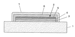
この実施の形態に係るEL装置の断面を図1に示す。基板として透明なガラス基板1が用いられ、そのガラス基板1の上に有機EL素子2が形成されている。有機EL素子2は、ガラス基板1の表面上に形成された第1の電極層となる陽極3と、陽極3の上に形成された発光層である有機発光層4と、有機発光層4の上に形成された第2の電極層となる陰極5とを有している。そして、このような有機EL素子2全体を覆うように、該有機EL素子2の表面上には第1の封止膜6が形成され、さらに第1の封止膜6を覆うように該第1の封止膜6の表面上に第2の封止膜7が形成されている。
Embodiments of the present invention will be described below with reference to the accompanying drawings.
A cross section of an EL device according to this embodiment is shown in FIG. A transparent glass substrate 1 is used as a substrate, and an organic EL element 2 is formed on the glass substrate 1. The organic EL element 2 includes an anode 3 that is a first electrode layer formed on the surface of the glass substrate 1, an organic light emitting layer 4 that is a light emitting layer formed on the anode 3, and an organic light emitting layer 4. It has the cathode 5 used as the 2nd electrode layer formed on it. Then, a first sealing film 6 is formed on the surface of the organic EL element 2 so as to cover the whole organic EL element 2, and the first sealing film 6 is further covered so as to cover the first sealing film 6. A second sealing
基板は、可視光に対して透明または半透明の材料から形成されればよく、ガラス基板1の他、このような条件を満たす樹脂基板を用いることもできる。ガラス基板1の上に形成された有機EL素子2の陽極3は、電極としての機能を有し且つ少なくとも可視光に対して透明または半透明であればよく、例えばITOがその材料として採用される。有機発光層4の材料としては、例えば、Alq3やDCMなどの公知の有機発光材料が含有される。また、電極間には、電子輸送層、電子注入層、ホール輸送層、ホール注入層等の公知の有機EL装置に採用される一または複数の層も適宜形成でき、各層は公知の材料から適宜形成される。有機発光層4を挟んで陽極3と反対側に形成される陰極5は、電極としての機能を有しておればよく、例えばAl、Cr、Mo、Al合金、Al/Mo積層体等の光反射性電極やITO等の透明電極が採用される。なお、各層は、真空蒸着法などの公知の薄膜形成法によって形成される。 The substrate only needs to be formed of a material that is transparent or translucent to visible light. In addition to the glass substrate 1, a resin substrate that satisfies such conditions can also be used. The anode 3 of the organic EL element 2 formed on the glass substrate 1 may have a function as an electrode and be at least transparent or translucent with respect to visible light. For example, ITO is adopted as the material thereof. . As a material of the organic light emitting layer 4, for example, a known organic light emitting material such as Alq 3 or DCM is contained. In addition, one or a plurality of layers employed in known organic EL devices such as an electron transport layer, an electron injection layer, a hole transport layer, and a hole injection layer can be appropriately formed between the electrodes, and each layer can be appropriately formed from a known material. It is formed. The cathode 5 formed on the opposite side of the anode 3 with the organic light emitting layer 4 interposed therebetween is only required to have a function as an electrode. For example, light of Al, Cr, Mo, Al alloy, Al / Mo laminate, etc. A reflective electrode or a transparent electrode such as ITO is employed. Each layer is formed by a known thin film forming method such as a vacuum evaporation method.
第1の封止膜6としては、乾式法により形成される無機材料膜が用いられる。無機材料としては、例えば、SiN、SiON及びSiO等のSi化合物が用いられる。乾式法としては、例えば、プラズマCVD法やスパッタ法が用いられ、第1の封止膜6は、有機発光層4のガラス転移点以下の温度で形成される。また、第1の封止膜6は、膜厚が0.1〜5μmに形成される。
第2の封止膜7は、塗料組成物を用いた湿式法により形成される。塗布法やディッピング法等の公知の湿式法により形成される第2の封止膜7は、第1の封止膜6の欠陥部分を穴埋めするように、第1の封止膜6の表面上に形成される。第2の封止膜7は、膜厚が、0.1〜30μmに形成される。ここで、塗料組成物は、水酸基またはシリル基を有する高分子及びポリシラザンを含む原料高分子と、原料高分子を溶解する乾燥溶媒との混合物からなる。したがって、第2の封止膜7は、高分子からなる有機部と、シリカからなる無機部とをもつ有機−無機ナノコンポジット膜として構成される。
As the first sealing film 6, an inorganic material film formed by a dry method is used. As the inorganic material, for example, Si compounds such as SiN, SiON, and SiO are used. As the dry method, for example, a plasma CVD method or a sputtering method is used, and the first sealing film 6 is formed at a temperature below the glass transition point of the organic light emitting layer 4. The first sealing film 6 is formed to a thickness of 0.1 to 5 μm.
The
水酸基を有する高分子は、例えば、水酸基を有するスチレン類や水酸基を有するアクリル樹脂などが使用できる。また、水酸基を有する高分子は、水酸基をもつ単量体を導入した重合体であってもよい。この場合、高分子の有する水酸基の量や導入位置が調整可能となる。尚、水酸基を有する単量体としては、3−ビニルフェノール、ヒドロキシメチルスチレン、4−ビニルベンジル−4−ヒドロキシブチルエーテル、4−(ヒドロキシメチルシリルフェニル)スチレン、などの水酸基を有するスチレン類や、ヒドロキシエチルメタクリレートなどの水酸基を有するアクリル樹脂や、N−(4−(4−ヒドロキシフェニルスルホニル)フェノキシカルボニル)メタクリルアミドなどの水酸基を有するアクリルアミド樹脂などが使用できる。これらの水酸基を有する単量体は、2種類以上を混合して用いてもよい。 Examples of the polymer having a hydroxyl group include styrenes having a hydroxyl group and acrylic resins having a hydroxyl group. Further, the polymer having a hydroxyl group may be a polymer into which a monomer having a hydroxyl group is introduced. In this case, the amount of hydroxyl groups and the introduction position of the polymer can be adjusted. Examples of the monomer having a hydroxyl group include styrenes having a hydroxyl group such as 3-vinylphenol, hydroxymethylstyrene, 4-vinylbenzyl-4-hydroxybutyl ether, 4- (hydroxymethylsilylphenyl) styrene, and hydroxy. An acrylic resin having a hydroxyl group such as ethyl methacrylate or an acrylamide resin having a hydroxyl group such as N- (4- (4-hydroxyphenylsulfonyl) phenoxycarbonyl) methacrylamide may be used. Two or more kinds of these monomers having a hydroxyl group may be mixed and used.
シリル基を有する高分子は、例えば、シリル基を有するスチレン類、シリル基を有するアクリル系樹脂などが使用できる。また、シリル基を有する高分子は、シリル基をもつ単量体を導入した重合体であってもよい。この場合、高分子の有するシリル基の量や導入位置が調整可能となる。尚、シリル基を有する単量体としては、トリメチルシリル−4−ビニルベンゾエート、1−トリメチルシリルオキシ−4−ビニルベンゼン、1−フェニルビニルトリメチルシリルエーテルなどのシリル基を有するスチレン類、2−トリメチルシリルオキシエチルメタクリレート、トリメチルシリルアクリレートなどのシリル基を有するアクリル樹脂、N(トリメチルシリルオキシ)メチルアクリルアミド、N(トリメチルシリル)メタクリルアミドなどのシリル基を有するアクリルアミド樹脂、イソプロペニルオキシトリメチルシラン、ジメチルエトキシビニルシランなどのシリル基を有するポリビニルアルコール樹脂等が使用できる。尚、シリル基を有する単量体は、これらのうちの1種類または2種類以上を併用してもよい。 As the polymer having a silyl group, for example, styrenes having a silyl group, acrylic resins having a silyl group, and the like can be used. Further, the polymer having a silyl group may be a polymer into which a monomer having a silyl group is introduced. In this case, the amount and introduction position of the silyl group that the polymer has can be adjusted. Examples of the monomer having a silyl group include styrenes having a silyl group such as trimethylsilyl-4-vinylbenzoate, 1-trimethylsilyloxy-4-vinylbenzene, 1-phenylvinyltrimethylsilyl ether, and 2-trimethylsilyloxyethyl methacrylate. Acrylic resins having a silyl group such as trimethylsilyl acrylate, acrylamide resins having a silyl group such as N (trimethylsilyloxy) methylacrylamide, N (trimethylsilyl) methacrylamide, silyl groups such as isopropenyloxytrimethylsilane and dimethylethoxyvinylsilane A polyvinyl alcohol resin etc. can be used. In addition, the monomer which has a silyl group may use together 1 type or 2 types or more of these.
水酸基またはシリル基をもつ単量体を導入した重合体は、その重合方法に特に限定はなく、それらの種類に合った重合方法を適宜選択すればよい。通常は、ラジカル重合や、アニオン重合、カチオン重合、メタセシス重合、リビングカチオン重合などの方法で重合される。 The polymer introduced with a monomer having a hydroxyl group or a silyl group is not particularly limited in its polymerization method, and a polymerization method suitable for the type thereof may be selected as appropriate. Usually, polymerization is performed by a method such as radical polymerization, anionic polymerization, cationic polymerization, metathesis polymerization, or living cationic polymerization.
ポリシラザンは、(−Si−N−)nで表される重合体からなり、通常、Si(珪素原子:4価)の2つの結合手およびN(窒素原子:3価)の1つの結合手には、水素原子や有機基が結合している。また、珪素原子や窒素原子の結合手には、他の珪素原子や窒素原子が結合してもよく、その場合は、環状構造や架橋構造を有するポリシラザンとなる。そして、ポリシラザンは、水及び酸素の存在下で分解し、窒素原子と酸素原子とが置換する転化反応により硬化し、シリカとなる。 Polysilazane is composed of a polymer represented by (-Si-N-) n , and usually has two bonds of Si (silicon atom: tetravalent) and one bond of N (nitrogen atom: trivalent). Is bonded to a hydrogen atom or an organic group. Further, another silicon atom or nitrogen atom may be bonded to the bond of the silicon atom or nitrogen atom, and in that case, polysilazane having a cyclic structure or a crosslinked structure is obtained. Polysilazane is decomposed in the presence of water and oxygen, and is cured by a conversion reaction in which nitrogen atoms and oxygen atoms are substituted to form silica.
ポリシラザンは、通常、シリカの被膜の形成に用いられているポリシラザンであれば特に限定はない。特に好ましいのは、ペルヒドロポリシラザン(PHPS)である。PHPSは、硬化温度が低いため、本発明に適したポリシラザンである。また、部分メチル化ペルヒドロポリシラザンを用いてもよい。なお、2種類以上のポリシラザンを混合して用いてもよい。 The polysilazane is not particularly limited as long as it is a polysilazane usually used for forming a silica film. Particularly preferred is perhydropolysilazane (PHPS). PHPS is a polysilazane suitable for the present invention because of its low curing temperature. Alternatively, partially methylated perhydropolysilazane may be used. Two or more types of polysilazane may be mixed and used.
尚、ポリシラザンの分子量については特に限定はないが、ポリシラザンの乾燥溶媒への溶解のしやすさや成膜性の観点から、その数平均分子量が50〜10,000、さらには、500〜2,000であるのが好ましい。 The molecular weight of polysilazane is not particularly limited, but from the viewpoint of ease of dissolution of polysilazane in a dry solvent and film forming properties, the number average molecular weight is 50 to 10,000, and further 500 to 2,000. Is preferred.
水酸基またはシリル基を有する高分子とポリシラザンとの割合については特に限定はないが、ポリシラザンの割合が多いほど、形成される第2の封止膜7の硬度は高くなる。具体的には、ポリシラザンは、原料高分子に対して10重量%以上であるのが好ましい。ポリシラザンンが10重量%以上であれば、十分な硬度を有する第2の封止膜7を得ることができる。また、ポリシラザンは95重量%以下であるのが好ましく、これにより、第2の封止膜7に生じる割れや剥離が抑制される。したがって、ポリシラザンは、10〜95重量%であるのが好ましく、さらに好ましくは15〜95重量%である。
The ratio between the polymer having a hydroxyl group or a silyl group and polysilazane is not particularly limited, but the greater the ratio of polysilazane, the higher the hardness of the formed second sealing
乾燥溶媒は、原料高分子を溶解し、ポリシラザンが加水分解されてゲル化しない程度まで脱水された溶媒である。溶媒に水が含まれると、水との反応により塗料組成物のゲル化が進み好ましくないため、乾燥材を用いるなどの方法により溶媒から水分を除去する。また、ポリシラザンは水酸基及びシリル基と反応しやすいため、水酸基及びシリル基を含まない溶媒を用いるのがよい。具体的には、芳香族炭化水素としては、ベンゼン、トルエン、キシレンなど、エステルとしては、酢酸エチル、酢酸n−ブチルなど、ケトン類としては、アセトン、メチルエチルケトンなど、エーテル類としては、ジエチルエーテル、ジオキサン、テトラヒドロフランなど、また、クロロホルムやピリジン等が挙げられる。特に好ましいのは、酢酸エチルであり、上記溶媒のうちの1種類または2種類以上を混合して乾燥溶媒として用いればよい。 The dry solvent is a solvent in which the raw material polymer is dissolved and dehydrated to such an extent that the polysilazane is not hydrolyzed and gelled. If water is contained in the solvent, gelation of the coating composition proceeds due to reaction with water, which is not preferable. Therefore, moisture is removed from the solvent by a method such as using a desiccant. Further, since polysilazane easily reacts with a hydroxyl group and a silyl group, it is preferable to use a solvent not containing a hydroxyl group and a silyl group. Specifically, as aromatic hydrocarbons, benzene, toluene, xylene, etc., as esters, ethyl acetate, n-butyl acetate, etc., as ketones, acetone, methyl ethyl ketone, etc., as ethers, diethyl ether, Examples include dioxane and tetrahydrofuran, and chloroform and pyridine. Particularly preferred is ethyl acetate, which may be used as a dry solvent by mixing one or more of the above solvents.
ところが、水酸基またはシリル基を有する高分子に対して良溶媒である乾燥溶媒は、耐薬品性の低い材料に対しても良溶媒であるため、例えば、樹脂基板に塗料組成物を塗布すると塗料組成物との接触面で溶解して劣化するおそれがある。そこで、乾燥溶媒として、水酸基またはシリル基を有する高分子及びポリシラザンに対して良溶媒である第1乾燥溶媒と、少なくとも水酸基またはシリル基を有する高分子に対して貧溶媒である第2乾燥溶媒とからなる混合乾燥溶媒を用いてもよい。つまり、第2乾燥溶媒は、水酸基またはシリル基を有する高分子に対して貧溶媒であるがポリシラザンに対しては良溶媒であってもよい。 However, a dry solvent that is a good solvent for a polymer having a hydroxyl group or a silyl group is also a good solvent for a material having low chemical resistance. For example, when a coating composition is applied to a resin substrate, the coating composition There is a risk of melting and degradation at the contact surface with the object. Therefore, as a dry solvent, a first dry solvent that is a good solvent for a polymer having a hydroxyl group or a silyl group and polysilazane, and a second dry solvent that is a poor solvent for a polymer having at least a hydroxyl group or a silyl group, A mixed dry solvent may be used. That is, the second dry solvent is a poor solvent for the polymer having a hydroxyl group or a silyl group, but may be a good solvent for the polysilazane.
第1乾燥溶媒及び第2乾燥溶媒としては、互いに混和し、混合乾燥溶媒としたときに原料高分子を分散可能な溶媒を選択して用いるのが好ましい。第1乾燥溶媒は、具体的には、乾燥溶媒の具体例として上述した溶媒と同じである。従って、第1乾燥溶媒として特に好ましいのは、酢酸エチルであり、それらのうちの1種類または2種類以上を併用してもよい。一方、第2乾燥溶媒は、シクロヘキサン、ペンタン、ヘキサン、ヘプタン、デカリン、灯油、石油などを用いることができる。特に好ましいのは、シクロヘキサンであり、これらのうちの1種類または2種類以上を併用してもよい。尚、第1乾燥溶媒と第2乾燥溶媒との組み合わせに特に限定はなく、用いる原料高分子の種類や量、成膜時の揮発条件等に応じて、上記の第1乾燥溶媒の1種類以上と上記の第2乾燥溶媒の1種類以上とを適宜選択して混合すればよい。 As the first dry solvent and the second dry solvent, it is preferable to select and use a solvent capable of dispersing the raw material polymer when mixed with each other to form a mixed dry solvent. Specifically, the first dry solvent is the same as the solvent described above as a specific example of the dry solvent. Accordingly, ethyl acetate is particularly preferable as the first dry solvent, and one or more of them may be used in combination. On the other hand, cyclohexane, pentane, hexane, heptane, decalin, kerosene, petroleum, etc. can be used as the second dry solvent. Particularly preferred is cyclohexane, and one or more of these may be used in combination. The combination of the first dry solvent and the second dry solvent is not particularly limited, and one or more types of the first dry solvent are used depending on the type and amount of the starting polymer used, volatilization conditions during film formation, and the like. And one or more of the second dry solvents may be appropriately selected and mixed.
第2乾燥溶媒の割合は、塗料組成物の調製方法、用いる原料高分子の種類や量、溶媒の種類にもよるが、混合乾燥溶媒に対して10〜90体積%であるのが好ましい。第2乾燥溶媒が10体積%以上であれば、塗料組成物を塗装する基板の劣化を良好に抑制することができる。第2乾燥溶媒が90体積%以下であれば、原料高分子のうち特に、水酸基またはシリル基を有する高分子を高濃度で用いることができる。また、当該高分子の濃度が高いと、塗料組成物の粘度が高くなるため、一度の塗装により膜厚の厚い塗装を形成することができる。第2乾燥溶媒は、さらに好ましくは、20〜80体積%であり、基板の劣化をさらに抑制できると共に、当該高分子をさらに高濃度で用いることができる。 The proportion of the second dry solvent is preferably 10 to 90% by volume based on the mixed dry solvent, although it depends on the method for preparing the coating composition, the type and amount of the starting polymer used, and the type of solvent. If the 2nd dry solvent is 10 volume% or more, degradation of the board | substrate which coats a coating composition can be suppressed favorably. When the second dry solvent is 90% by volume or less, a polymer having a hydroxyl group or a silyl group can be used at a high concentration among the raw material polymers. Moreover, since the viscosity of a coating composition will become high when the density | concentration of the said polymer is high, thick coating can be formed by one coating. The second dry solvent is more preferably 20 to 80% by volume, which can further suppress the deterioration of the substrate and can use the polymer at a higher concentration.
また、水酸基またはシリル基を有する高分子は、塗料組成物に対して10〜90重量%、さらに好ましくは30〜65重量%含むのがよい。当該高分子の配合量がこの範囲にあれば、分子量にもよるが、塗料組成物は基板に塗布しやすく、成膜性にも優れる。 Further, the polymer having a hydroxyl group or a silyl group may be contained in an amount of 10 to 90% by weight, more preferably 30 to 65% by weight, based on the coating composition. If the blending amount of the polymer is within this range, the coating composition can be easily applied to the substrate and has excellent film formability, although it depends on the molecular weight.
尚、この塗料組成物は、上記の実施形態に限定されるものではなく、他の機能を追加するために、必要に応じて、乾燥促進剤や紫外線吸収剤、帯電防止剤などの別の物質を混合してもよい。 In addition, this coating composition is not limited to the above-described embodiment, and other substances such as a drying accelerator, an ultraviolet absorber, and an antistatic agent are added as necessary to add other functions. May be mixed.
次に、この実施の形態に係るEL装置の製造方法について説明する。
まず、ガラス基板1の表面上に真空蒸着法等の公知の薄膜形成法により陽極3、有機発光層4及び陰極5を順次積層して有機EL素子2を形成する。その後、ガラス基板1を真空中あるいは不活性雰囲気中でプラズマCVD装置のチャンバ内まで搬送し、プラズマCVD法により陰極5の表面上に第1の封止膜6を形成する。このとき、有機EL素子2に悪影響を与えないために、ガラス基板1がEL素子2を構成する各材料のガラス転移温度以下の温度域、例えば、50〜110℃で第1の封止膜6の形成を行うことが好ましい。また、ガラス基板1がEL素子2を構成する各材料のガラス転移温度のうち最も低い温度より20K低い温度域となるような条件で第1の封止膜6を形成することがさらに好ましい。
Next, a method for manufacturing the EL device according to this embodiment will be described.
First, the organic EL element 2 is formed by sequentially laminating the anode 3, the organic light emitting layer 4, and the cathode 5 on the surface of the glass substrate 1 by a known thin film forming method such as a vacuum deposition method. Thereafter, the glass substrate 1 is transferred into a chamber of a plasma CVD apparatus in a vacuum or in an inert atmosphere, and a first sealing film 6 is formed on the surface of the cathode 5 by plasma CVD. At this time, in order not to adversely affect the organic EL element 2, the first sealing film 6 is formed in a temperature range below the glass transition temperature of each material constituting the EL element 2 by the glass substrate 1, for example, 50 to 110 ° C. It is preferable to form Further, it is more preferable that the first sealing film 6 is formed under such a condition that the glass substrate 1 is in a temperature range that is 20K lower than the lowest temperature among the glass transition temperatures of the materials constituting the EL element 2.
第1の封止膜6の形成終了後、大気開放して、調製した塗料組成物を第1の封止膜6の表面上に塗布する。塗布方法としては、スピン法、ディップ法、フロー法、ロールコート法、スクリーン印刷法等の各種の方法を用いることができる。また、大気開放せずに、第1の封止膜6を形成したときの雰囲気中あるいは不活性雰囲気中で塗布することもできる。
その後、塗布した塗料組成物を硬化させる硬化工程へと移行する。硬化工程では、水と酸素の存在下において、乾燥溶媒を揮発させると共にポリシラザンの分子をシリカへと転化させる。これにより、第2の封止膜7が形成される。
さらに、塗料組成物中の高分子や基材、有機EL素子の形成材料を劣化させない程度の温度であれば、硬化工程においてオーブン、ホットプレート等の加熱装置を用いてベーキング処理することによりポリシラザンのシリカへの転化を促進させることも可能であり、より短時間で塗料組成物を硬化させることができる。
これにより、EL装置が製造される。
After completion of the formation of the first sealing film 6, the atmosphere is released and the prepared coating composition is applied onto the surface of the first sealing film 6. As a coating method, various methods such as a spin method, a dipping method, a flow method, a roll coating method, and a screen printing method can be used. Moreover, it can also apply | coat in the atmosphere at the time of forming the 1st sealing film 6 or inactive atmosphere, without air-releasing.
Then, it transfers to the hardening process which hardens the apply | coated coating composition. In the curing step, in the presence of water and oxygen, the dry solvent is volatilized and the polysilazane molecules are converted to silica. Thereby, the
Further, if the temperature is such that the polymer, the base material, and the organic EL element forming material in the coating composition are not deteriorated, the polysilazane can be baked by baking using a heating device such as an oven or a hot plate in the curing process. Conversion to silica can also be promoted, and the coating composition can be cured in a shorter time.
Thereby, an EL device is manufactured.
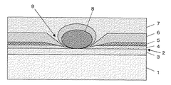
図2に示されるように、例えば有機EL素子2の表面上に埃等の極微小な異物8が存在した場合、乾式法で有機EL素子2の表面に第1の封止膜6を形成したとても、乾式法は膜の付け回り性が良好でないため、その異物を完全に覆いきることができずに、有機EL素子2の表面に第1の封止膜6の未付着部分9が生じるおそれがある。しかし、本発明では、第1の封止膜6の上に膜の付け回り性の良好な湿式法により第2の封止膜7を形成するため、この第2の封止膜7が第1の封止膜6の未付着部分9を穴埋めすることとなる。従って、外部から有機EL素子2への水分の浸入を防止することができる。
As shown in FIG. 2, for example, when a very small foreign matter 8 such as dust is present on the surface of the organic EL element 2, the first sealing film 6 is formed on the surface of the organic EL element 2 by a dry method. Since the dry method does not have a good film throwing power, the foreign matter cannot be completely covered, and the non-attached portion 9 of the first sealing film 6 may be formed on the surface of the organic EL element 2. There is. However, in the present invention, since the
このように、この実施の形態に係るEL装置は、水酸基またはシリル基を有する高分子及びポリシラザンを含む原料高分子と乾燥溶媒とからなる塗料組成物を第1の封止膜6の表面上に塗布し、ポリシラザンをシリカに転化させて塗料組成物を硬化させることにより、第1の封止膜6を覆うように第2の封止膜7が形成されている。第2の封止膜7は、水酸基またはシリル基を有する高分子からなる有機部と、水酸基またはシリル基の周囲に位置するシリカからなる無機部とをもつ有機−無機ナノコンポジットとなる。すなわち、第2の封止膜7は、有機物及び無機物の性質を合わせもつことになり、高い封止性と高い硬度とを有しながら、割れや剥がれが生じにくくなる。これにより、第1の封止膜6及び第2の封止膜7の他に保護フィルムを設ける必要がなくなるので、EL装置の厚さを薄くすることができる。
As described above, in the EL device according to this embodiment, a coating composition composed of a polymer having a hydroxyl group or a silyl group and a raw material polymer containing polysilazane and a drying solvent is formed on the surface of the first sealing film 6. The
この実施の形態では、ガラス基板1上に透明性の陽極3、有機発光層4及び反射性の陰極5が順次積層され、有機発光層4で発した光が陽極3及びガラス基板1を透過して出射されるボトムエミッション型の有機EL装置について説明したが、これに限るものではなく、この発明は、基板上に反射性電極、有機発光層及び透明性電極を順次積層して有機発光層で発した光が基板とは反対側の透明性電極を透過して出射されるトップエミッション型の有機EL装置にも適用される。この場合、透明性電極の上に第1の封止膜及び第2の封止膜が順次形成されるが、これら第1の封止膜及び第2の封止膜は、可視光に対して透明または半透明の材料から形成する必要がある。 In this embodiment, a transparent anode 3, an organic light emitting layer 4 and a reflective cathode 5 are sequentially laminated on a glass substrate 1, and light emitted from the organic light emitting layer 4 passes through the anode 3 and the glass substrate 1. However, the present invention is not limited to this, and the present invention is not limited to this, and the present invention provides an organic light emitting layer in which a reflective electrode, an organic light emitting layer, and a transparent electrode are sequentially laminated on a substrate. The present invention is also applied to a top emission type organic EL device in which emitted light is transmitted through a transparent electrode on the side opposite to the substrate. In this case, the first sealing film and the second sealing film are sequentially formed on the transparent electrode, and the first sealing film and the second sealing film are formed with respect to visible light. It must be formed from a transparent or translucent material.
以下に、この発明の実施例を、表を用いて説明する。 Hereinafter, embodiments of the present invention will be described with reference to tables.
[有機EL素子の製造]
透明なガラス基板上に反応性スパッタにより厚さ190nmの陽極ITOを形成した。その後、発光層の蒸着に先立つ基板洗浄として、ガラス基板をアルカリ洗浄し、次いで純水洗浄し、乾燥させて紫外線オゾン洗浄を行った。ガラス基板を真空蒸着装置へ移し、陽極の表面上にホール注入領域として銅フタロシアニンをカーボンるつぼで蒸着速度0.1nm/s、真空度約5.0×10−5Paで厚さ10nm蒸着した。
[Manufacture of organic EL elements]
An anode ITO having a thickness of 190 nm was formed on a transparent glass substrate by reactive sputtering. Thereafter, as a substrate cleaning prior to vapor deposition of the light emitting layer, the glass substrate was washed with an alkali, then washed with pure water, dried and subjected to ultraviolet ozone cleaning. The glass substrate was transferred to a vacuum deposition apparatus, and copper phthalocyanine was deposited on the surface of the anode as a hole injection region with a carbon crucible at a deposition rate of 0.1 nm / s and a vacuum degree of about 5.0 × 10 −5 Pa to a thickness of 10 nm.
次に、ホール注入領域の上にホール輸送領域としてトリフェニルアミンの4量体をカーボンるつぼで蒸着速度0.1nm/s、真空度約5.0×10−5Paで厚さ30nm蒸着した。さらに、ホール輸送領域の上に発光領域としてDPVBi(発光色:青)を蒸着速度0.1nm/s、真空度約5.0×10−5Paで厚さ30nm蒸着した。 Next, a tetraphenylamine tetramer was deposited as a hole transport region on the hole injection region with a carbon crucible at a deposition rate of 0.1 nm / s and a vacuum degree of about 5.0 × 10 −5 Pa to a thickness of 30 nm. Furthermore, DPVBi (emission color: blue) was deposited as a light emitting region on the hole transport region at a deposition rate of 0.1 nm / s and a degree of vacuum of about 5.0 × 10 −5 Pa to a thickness of 30 nm.
発光領域の上に電子輸送領域としてキノリノラト系金属錯体であるAlq3をカーボンるつぼで蒸着速度0.01nm/s、真空度約5.0×10−5Paで厚さ20nm蒸着した。その後、電子輸送領域の上に陰極界面領域としてLiFをカーボンるつぼで蒸着速度0.03nm/s、真空度約5.0×10−5Paで厚さ0.5nm蒸着し、さらに陰極界面領域の上に陰極としてアルミニウムをタングステンボートで蒸着速度1nm/s、真空度約5.0×10−5Paで厚さ100nm蒸着した。 Depositing Alq 3 is a quinolinolato metal complex as the electron transport region on the light emitting region in a carbon crucible rate 0.01 nm / s, and a thickness of 20nm degree of vacuum of about 5.0 × 10 -5 Pa. Thereafter, LiF was deposited on the electron transport region as a cathode interface region with a carbon crucible at a deposition rate of 0.03 nm / s and a vacuum degree of about 5.0 × 10 −5 Pa to a thickness of 0.5 nm. On the top, aluminum was deposited as a cathode with a tungsten boat at a deposition rate of 1 nm / s and a degree of vacuum of about 5.0 × 10 −5 Pa to a thickness of 100 nm.
[第1の封止膜の形成]
このようにしてガラス基板上に有機EL素子を形成した後、陰極の表面上にプラズマCVD装置により第1の保護膜としてSiN膜を形成した。すなわち、ガラス基板をプラズマCVD装置のチャンバ内に入れて圧力1×10⁻³Paまで排気し、SiH4を100ml、NH3を50ml、N2を1000ml流し、圧力を75Paに調整した。次に、ギャップ20mmの一対の電極に13.56MHz、600Wの高周波電力を供給し、ガスを放電させることにより陰極の表面上に厚さ1μmのSiN膜を堆積させた。なお、このときガラス基板の温度が100℃以下となるように設定し、成膜速度は約3nm/sであった。
[Formation of first sealing film]
After forming the organic EL element on the glass substrate in this way, a SiN film was formed as a first protective film on the surface of the cathode by a plasma CVD apparatus. That is, the glass substrate was placed in a chamber of a plasma CVD apparatus and evacuated to a pressure of 1 × 10 −3 Pa, and 100 ml of SiH 4 , 50 ml of NH 3 and 1000 ml of N 2 were flowed to adjust the pressure to 75 Pa. Next, high frequency power of 13.56 MHz and 600 W was supplied to a pair of electrodes with a gap of 20 mm, and a gas was discharged to deposit a 1 μm thick SiN film on the surface of the cathode. At this time, the temperature of the glass substrate was set to 100 ° C. or lower, and the film formation rate was about 3 nm / s.
[第2の封止膜の形成]
[塗料組成物の調製]
[塗料組成物1]
シリル基を有する高分子として、ポリ(メチルメタクリレート−co−2−(トリメチルシリルオキシ)エチルメタクリレート)を原子移動ラジカル重合により合成した。各成分は、メチルメタクリレート:94.3mol%、(トリメチルシリルオキシ)エチルメタクリレート:5.7mol%、数平均分子量は1.45×10⁴であった。尚、高分子の各成分のモル分率は、1H原子を用いた核磁気共鳴吸収法(NMR)により、また、数平均分子量は、ゲル浸透クロマトグラフィー(GPC)により測定した。
[Formation of Second Sealing Film]
[Preparation of coating composition]
[Coating composition 1]
As a polymer having a silyl group, poly (methyl methacrylate-co-2- (trimethylsilyloxy) ethyl methacrylate) was synthesized by atom transfer radical polymerization. Each component was methyl methacrylate: 94.3 mol%, (trimethylsilyloxy) ethyl methacrylate: 5.7 mol%, and the number average molecular weight was 1.45 × 10 4 . The molar fraction of each component of the polymer was measured by nuclear magnetic resonance absorption (NMR) using 1 H atoms, and the number average molecular weight was measured by gel permeation chromatography (GPC).
次に、高分子227.25mgを、金属ナトリウムにより脱水された11.1mlの酢酸エチル(第1乾燥溶媒)に溶解した。その後、窒素雰囲気下にて、ペルヒドロポリシラザン−ジブチルエーテル溶液(AZエレクトロニックマテリアルズ製NL−120)を2ml加え、10分間攪拌した。攪拌後の混合溶液に、大気下にて、9mlのシクロヘキサン(第2乾燥溶媒)を一度に添加して攪拌し、塗料組成物1を得た。 Next, 227.25 mg of the polymer was dissolved in 11.1 ml of ethyl acetate (first dry solvent) dehydrated with sodium metal. Thereafter, 2 ml of a perhydropolysilazane-dibutyl ether solution (NL-120 manufactured by AZ Electronic Materials) was added under a nitrogen atmosphere and stirred for 10 minutes. To the mixed solution after stirring, 9 ml of cyclohexane (second dry solvent) was added at once in the atmosphere and stirred to obtain a coating composition 1.
[塗料組成物2]
塗料組成物1の調製で使用したポリ(メチルメタクリレート−co−2−(トリメチルシリルオキシ)エチルメタクリレート)にかえて、水酸基を有する高分子として各成分が、メチルメタクリレート:86.3mol%、ヒドロキシエチルメタクリレート:13.7mol%、数平均分子量は3.3×10⁴である原子移動ラジカル重合により合成したポリ(メチルメタクリレート−co−2−ヒドロキシエチルメタクリレート)を用いた他は、塗料組成物1と同様にして塗料組成物2を調製した。
[Coating composition 2]
Instead of poly (methyl methacrylate-co-2- (trimethylsilyloxy) ethyl methacrylate) used in the preparation of the coating composition 1, each component as a polymer having a hydroxyl group is methyl methacrylate: 86.3 mol%, hydroxyethyl methacrylate. : 13.7 mol%, and the number average molecular weight is 3.3 × 10 4 except that poly (methyl methacrylate-co-2-hydroxyethyl methacrylate) synthesized by atom transfer radical polymerization was used. Thus, a coating composition 2 was prepared.
[塗料組成物1及び2の塗布及び硬化]
調製された塗料組成物1及び2を、調製後直ちに、製造されたEL素子の第1の封止膜の表面上に、スプレーコート法により塗布した。塗布後、室温で24時間乾燥し、100℃で3時間焼成した。これにより、塗料組成物1によって第2の封止膜が形成されたEL装置1と、塗料組成物2によって第2の封止膜が形成されたEL装置2とを得た。
[Coating and curing of coating compositions 1 and 2]
The prepared coating compositions 1 and 2 were applied by spray coating on the surface of the first sealing film of the manufactured EL device immediately after the preparation. After coating, the film was dried at room temperature for 24 hours and baked at 100 ° C. for 3 hours. Thereby, the EL device 1 in which the second sealing film was formed by the coating composition 1 and the EL device 2 in which the second sealing film was formed by the coating composition 2 were obtained.
EL装置1及び2について、封止性能を測定した。EL装置1及び2のそれぞれを、100℃で3時間の焼成後、室温で71時間放置し、次に、温度60℃、相対湿度90%の条件で674時間の高温高湿評価を実施した。その結果、EL装置1及び2の両方とも、484時間まではダークスポットの発生は認められなかった。 The sealing performance of the EL devices 1 and 2 was measured. Each of the EL devices 1 and 2 was baked at 100 ° C. for 3 hours and then allowed to stand at room temperature for 71 hours, and then evaluated for high temperature and high humidity for 674 hours under conditions of a temperature of 60 ° C. and a relative humidity of 90%. As a result, in both EL devices 1 and 2, no dark spots were observed until 484 hours.
1 ガラス基板(基板)、2 有機EL素子、3 陽極(第1の電極層)、4 有機発光層(発光層)、5 陰極(第2の電極層)、6 第1の封止膜、7 第2の封止膜。 DESCRIPTION OF SYMBOLS 1 Glass substrate (board | substrate), 2 Organic EL element, 3 Anode (1st electrode layer), 4 Organic light emitting layer (light emitting layer), 5 Cathode (2nd electrode layer), 6 1st sealing film, 7 Second sealing film.
Claims (6)
前記有機EL素子を覆うように該有機EL素子の表面上に乾式法により形成された無機材料からなる第1の封止膜と、
該第1の封止膜の表面上に塗料組成物を用いた湿式法により形成された第2の封止膜と
を備え、
前記塗料組成物は、水酸基を有する高分子及びポリシラザンを含む原料高分子と、該原料高分子を溶解する乾燥溶媒との混合物からなる
ことを特徴とするEL装置。 In an EL device in which an organic EL element having at least a first electrode layer, a light emitting layer, and a second electrode layer is formed on a substrate,
A first sealing film made of an inorganic material formed by a dry method on the surface of the organic EL element so as to cover the organic EL element;
A second sealing film formed on the surface of the first sealing film by a wet method using a coating composition;
2. The EL device according to claim 1, wherein the coating composition comprises a mixture of a raw material polymer containing a polymer having a hydroxyl group and polysilazane and a dry solvent for dissolving the raw material polymer.
前記有機EL素子を覆うように該有機EL素子の表面上に乾式法により形成された無機材料からなる第1の封止膜と、
該第1の封止膜の表面上に塗料組成物を用いた湿式法により形成された第2の封止膜と
を備え、
前記塗料組成物は、シリル基を有する高分子及びポリシラザンを含む原料高分子と、該原料高分子を溶解する乾燥溶媒との混合物からなる
ことを特徴とするEL装置。 In an EL device in which an organic EL element having at least a first electrode layer, a light emitting layer, and a second electrode layer is formed on a substrate,
A first sealing film made of an inorganic material formed by a dry method on the surface of the organic EL element so as to cover the organic EL element;
A second sealing film formed on the surface of the first sealing film by a wet method using a coating composition;
2. The EL device according to claim 1, wherein the coating composition comprises a mixture of a raw material polymer containing a silyl group-containing polymer and polysilazane and a dry solvent for dissolving the raw material polymer.
前記高分子及び前記ポリシラザンに対して良溶媒である第1乾燥溶媒と、
少なくとも前記高分子に対して貧溶媒である第2乾燥溶媒と
を含む、請求項1または2に記載のEL装置。 The dry solvent is
A first dry solvent that is a good solvent for the polymer and the polysilazane;
The EL device according to claim 1, comprising at least a second dry solvent that is a poor solvent for the polymer.
Priority Applications (1)
| Application Number | Priority Date | Filing Date | Title |
|---|---|---|---|
| JP2008100064A JP2009252574A (en) | 2008-04-08 | 2008-04-08 | El device |
Applications Claiming Priority (1)
| Application Number | Priority Date | Filing Date | Title |
|---|---|---|---|
| JP2008100064A JP2009252574A (en) | 2008-04-08 | 2008-04-08 | El device |
Publications (1)
| Publication Number | Publication Date |
|---|---|
| JP2009252574A true JP2009252574A (en) | 2009-10-29 |
Family
ID=41313088
Family Applications (1)
| Application Number | Title | Priority Date | Filing Date |
|---|---|---|---|
| JP2008100064A Pending JP2009252574A (en) | 2008-04-08 | 2008-04-08 | El device |
Country Status (1)
| Country | Link |
|---|---|
| JP (1) | JP2009252574A (en) |
Cited By (11)
| Publication number | Priority date | Publication date | Assignee | Title |
|---|---|---|---|---|
| JP2011138748A (en) * | 2010-01-04 | 2011-07-14 | Samsung Mobile Display Co Ltd | Organic light-emitting display device |
| KR101255537B1 (en) * | 2010-11-26 | 2013-04-16 | 삼성디스플레이 주식회사 | Flat display device and the manufacturing method thereof |
| EP2607412A1 (en) * | 2010-08-20 | 2013-06-26 | LINTEC Corporation | Molding, production method therefor, part for electronic devices and electronic device |
| WO2013125351A1 (en) * | 2012-02-21 | 2013-08-29 | リンテック株式会社 | Gas barrier structure and method for forming gas barrier structure |
| WO2013125352A1 (en) * | 2012-02-21 | 2013-08-29 | リンテック株式会社 | Organic electronic element and method for manufacturing organic electronic element |
| US8865810B2 (en) | 2009-03-26 | 2014-10-21 | Lintec Corporation | Formed article, method for producing same, electronic device member, and electronic device |
| US9340869B2 (en) | 2008-08-19 | 2016-05-17 | Lintec Corporation | Formed article, method for producing the same, electronic device member, and electronic device |
| US9365922B2 (en) | 2009-05-22 | 2016-06-14 | Lintec Corporation | Formed article, method of producing same, electronic device member, and electronic device |
| US9512334B2 (en) | 2011-09-08 | 2016-12-06 | Lintec Corporation | Modified polysilazane film and method for producing gas barrier film |
| US9540519B2 (en) | 2010-03-31 | 2017-01-10 | Lintec Corporation | Formed article, method for producing same, electronic device member, and electronic device |
| US9698370B2 (en) | 2012-01-20 | 2017-07-04 | Lintec Corporation | Gas barrier film and gas barrier film production method |
Citations (8)
| Publication number | Priority date | Publication date | Assignee | Title |
|---|---|---|---|---|
| JPH09175868A (en) * | 1995-12-27 | 1997-07-08 | Tonen Corp | Polycarbonate product covered with hard coat film and its production |
| JP2003282242A (en) * | 2002-03-25 | 2003-10-03 | Toyota Central Res & Dev Lab Inc | Organic electroluminescent (el) element and organic electronic device |
| JP2005056587A (en) * | 2003-08-01 | 2005-03-03 | Toyota Industries Corp | El device and manufacturing method thereof |
| JP2005232275A (en) * | 2004-02-18 | 2005-09-02 | Toyota Industries Corp | Coating material composition, method for producing transparent protective film using the same, and organic glass bearing the transparent protective film |
| JP2006244943A (en) * | 2005-03-07 | 2006-09-14 | Aitesu:Kk | Organic el element and its manufacturing method |
| JP2006328217A (en) * | 2005-05-26 | 2006-12-07 | Toyota Industries Corp | Coating composition and method for preparing coating composition |
| JP2006328220A (en) * | 2005-05-26 | 2006-12-07 | Toyota Industries Corp | Coating composition, method for preparing coating composition, method for producing transparent protective film using coating composition and organic glass having transparent protective film |
| JP2009096901A (en) * | 2007-10-18 | 2009-05-07 | Toyota Industries Corp | Coating composition, method for producing transparent protective film by using coating composition and organic glass having transparent protective film |
-
2008
- 2008-04-08 JP JP2008100064A patent/JP2009252574A/en active Pending
Patent Citations (8)
| Publication number | Priority date | Publication date | Assignee | Title |
|---|---|---|---|---|
| JPH09175868A (en) * | 1995-12-27 | 1997-07-08 | Tonen Corp | Polycarbonate product covered with hard coat film and its production |
| JP2003282242A (en) * | 2002-03-25 | 2003-10-03 | Toyota Central Res & Dev Lab Inc | Organic electroluminescent (el) element and organic electronic device |
| JP2005056587A (en) * | 2003-08-01 | 2005-03-03 | Toyota Industries Corp | El device and manufacturing method thereof |
| JP2005232275A (en) * | 2004-02-18 | 2005-09-02 | Toyota Industries Corp | Coating material composition, method for producing transparent protective film using the same, and organic glass bearing the transparent protective film |
| JP2006244943A (en) * | 2005-03-07 | 2006-09-14 | Aitesu:Kk | Organic el element and its manufacturing method |
| JP2006328217A (en) * | 2005-05-26 | 2006-12-07 | Toyota Industries Corp | Coating composition and method for preparing coating composition |
| JP2006328220A (en) * | 2005-05-26 | 2006-12-07 | Toyota Industries Corp | Coating composition, method for preparing coating composition, method for producing transparent protective film using coating composition and organic glass having transparent protective film |
| JP2009096901A (en) * | 2007-10-18 | 2009-05-07 | Toyota Industries Corp | Coating composition, method for producing transparent protective film by using coating composition and organic glass having transparent protective film |
Cited By (19)
| Publication number | Priority date | Publication date | Assignee | Title |
|---|---|---|---|---|
| US9340869B2 (en) | 2008-08-19 | 2016-05-17 | Lintec Corporation | Formed article, method for producing the same, electronic device member, and electronic device |
| US8865810B2 (en) | 2009-03-26 | 2014-10-21 | Lintec Corporation | Formed article, method for producing same, electronic device member, and electronic device |
| US9365922B2 (en) | 2009-05-22 | 2016-06-14 | Lintec Corporation | Formed article, method of producing same, electronic device member, and electronic device |
| US8735936B2 (en) | 2010-01-04 | 2014-05-27 | Samsung Display Co., Ltd. | Organic light emitting diode display |
| JP2011138748A (en) * | 2010-01-04 | 2011-07-14 | Samsung Mobile Display Co Ltd | Organic light-emitting display device |
| US9540519B2 (en) | 2010-03-31 | 2017-01-10 | Lintec Corporation | Formed article, method for producing same, electronic device member, and electronic device |
| JP5750441B2 (en) * | 2010-08-20 | 2015-07-22 | リンテック株式会社 | Molded body, manufacturing method thereof, member for electronic device, and electronic device |
| EP2607412A4 (en) * | 2010-08-20 | 2014-04-30 | Lintec Corp | Molding, production method therefor, part for electronic devices and electronic device |
| EP2607412A1 (en) * | 2010-08-20 | 2013-06-26 | LINTEC Corporation | Molding, production method therefor, part for electronic devices and electronic device |
| US9556513B2 (en) | 2010-08-20 | 2017-01-31 | Lintec Corporation | Molding, production method therefor, part for electronic devices and electronic device |
| US8492974B2 (en) | 2010-11-26 | 2013-07-23 | Samsung Display Co., Ltd. | Flat panel display device and method of manufacturing the same |
| KR101255537B1 (en) * | 2010-11-26 | 2013-04-16 | 삼성디스플레이 주식회사 | Flat display device and the manufacturing method thereof |
| US9512334B2 (en) | 2011-09-08 | 2016-12-06 | Lintec Corporation | Modified polysilazane film and method for producing gas barrier film |
| US9698370B2 (en) | 2012-01-20 | 2017-07-04 | Lintec Corporation | Gas barrier film and gas barrier film production method |
| JP5408818B1 (en) * | 2012-02-21 | 2014-02-05 | リンテック株式会社 | Gas barrier structure and method for forming gas barrier structure |
| WO2013125351A1 (en) * | 2012-02-21 | 2013-08-29 | リンテック株式会社 | Gas barrier structure and method for forming gas barrier structure |
| JPWO2013125352A1 (en) * | 2012-02-21 | 2015-07-30 | リンテック株式会社 | Organic electronic device and method for producing organic electronic device |
| WO2013125352A1 (en) * | 2012-02-21 | 2013-08-29 | リンテック株式会社 | Organic electronic element and method for manufacturing organic electronic element |
| US9577211B2 (en) | 2012-02-21 | 2017-02-21 | Lintec Corporation | Organic electronic element and method for manufacturing organic electronic element |
Similar Documents
| Publication | Publication Date | Title |
|---|---|---|
| JP2009252574A (en) | El device | |
| JP6041039B2 (en) | GAS BARRIER FILM, METHOD FOR PRODUCING GAS BARRIER FILM, AND ELECTRONIC DEVICE | |
| JP6056854B2 (en) | GAS BARRIER FILM, METHOD FOR PRODUCING GAS BARRIER FILM, AND ELECTRONIC DEVICE | |
| KR101452680B1 (en) | Gas barrier film, manufacturing process for gas barrier film, and electronic device | |
| US9163163B2 (en) | Multilayer film, method for manufacture thereof and articles including the same | |
| JP5803937B2 (en) | GAS BARRIER FILM, METHOD FOR PRODUCING GAS BARRIER FILM, AND ELECTRONIC DEVICE | |
| TWI270313B (en) | Organic EL device and method of manufacturing the same | |
| CN103958182B (en) | Gas barrier film and electronic equipment | |
| US20150331153A1 (en) | Gas barrier film, and method for manufacturing same | |
| JP2005111702A (en) | Gas barrier base material, display substrate and organic el display | |
| JP2013208867A (en) | Gas barrier film, and electronic device | |
| Zhang et al. | Stretchable PDMS encapsulation via SiO2 doping and atomic layer infiltration for flexible displays | |
| Wang et al. | A novel nucleation inducer for ultrathin au anodes in high efficiency and flexible organic optoelectronic devices | |
| JP2013180520A (en) | Gas barrier film and electronic device | |
| KR101481417B1 (en) | Gas barrier composition, encapsulation film and organic electroic device comprising the same | |
| KR101489959B1 (en) | Gas barrier film, method for preparing thereof and display display member comprising the same | |
| JP2011026645A (en) | Method for producing barrier film, barrier film and method for manufacturing organic photoelectric conversion element | |
| JP5928634B2 (en) | Gas barrier film and electronic device | |
| KR20100125134A (en) | Composition comprising an organic-inorganic hybrid compound, adhesive film and organic light emitting display | |
| KR102035909B1 (en) | Composition for gas barrier film, comprising bridged organosilica precursor and gar barrier film thereof | |
| JP2013052569A (en) | Method for manufacturing moisture vapor barrier film, moisture vapor barrier film, and electric equipment | |
| KR100601913B1 (en) | Organic silicate film for bright-enhanced organic light emitting diode | |
| JP4292519B2 (en) | Transparent gas barrier multilayer substrate | |
| JPH11183887A (en) | Liquid crystal display substrate | |
| JPH11241003A (en) | Resin composition for color filter protective film and color filter made therefrom |
Legal Events
| Date | Code | Title | Description |
|---|---|---|---|
| A621 | Written request for application examination |
Free format text: JAPANESE INTERMEDIATE CODE: A621 Effective date: 20100602 |
|
| A977 | Report on retrieval |
Free format text: JAPANESE INTERMEDIATE CODE: A971007 Effective date: 20111020 |
|
| A131 | Notification of reasons for refusal |
Free format text: JAPANESE INTERMEDIATE CODE: A131 Effective date: 20111025 |
|
| A02 | Decision of refusal |
Free format text: JAPANESE INTERMEDIATE CODE: A02 Effective date: 20120321 |