WO2010110219A1 - 光アイソレータ素子およびこれを用いた光モジュール - Google Patents
光アイソレータ素子およびこれを用いた光モジュール Download PDFInfo
- Publication number
- WO2010110219A1 WO2010110219A1 PCT/JP2010/054849 JP2010054849W WO2010110219A1 WO 2010110219 A1 WO2010110219 A1 WO 2010110219A1 JP 2010054849 W JP2010054849 W JP 2010054849W WO 2010110219 A1 WO2010110219 A1 WO 2010110219A1
- Authority
- WO
- WIPO (PCT)
- Prior art keywords
- polarizer
- metal particle
- optical isolator
- particle layer
- metal
- Prior art date
- Legal status (The legal status is an assumption and is not a legal conclusion. Google has not performed a legal analysis and makes no representation as to the accuracy of the status listed.)
- Ceased
Links
Images






Classifications
-
- G—PHYSICS
- G02—OPTICS
- G02F—OPTICAL DEVICES OR ARRANGEMENTS FOR THE CONTROL OF LIGHT BY MODIFICATION OF THE OPTICAL PROPERTIES OF THE MEDIA OF THE ELEMENTS INVOLVED THEREIN; NON-LINEAR OPTICS; FREQUENCY-CHANGING OF LIGHT; OPTICAL LOGIC ELEMENTS; OPTICAL ANALOGUE/DIGITAL CONVERTERS
- G02F1/00—Devices or arrangements for the control of the intensity, colour, phase, polarisation or direction of light arriving from an independent light source, e.g. switching, gating or modulating; Non-linear optics
- G02F1/01—Devices or arrangements for the control of the intensity, colour, phase, polarisation or direction of light arriving from an independent light source, e.g. switching, gating or modulating; Non-linear optics for the control of the intensity, phase, polarisation or colour
- G02F1/09—Devices or arrangements for the control of the intensity, colour, phase, polarisation or direction of light arriving from an independent light source, e.g. switching, gating or modulating; Non-linear optics for the control of the intensity, phase, polarisation or colour based on magneto-optical elements, e.g. exhibiting Faraday effect
- G02F1/093—Devices or arrangements for the control of the intensity, colour, phase, polarisation or direction of light arriving from an independent light source, e.g. switching, gating or modulating; Non-linear optics for the control of the intensity, phase, polarisation or colour based on magneto-optical elements, e.g. exhibiting Faraday effect used as non-reciprocal devices, e.g. optical isolators, circulators
Definitions
- the present invention relates to an optical isolator for blocking reflected return light to a light emitting element and an optical module using the same.
- An optical module equipped with a light emitting element is used for an optical communication device or a sensor light source.
- the optical isolator element has a Faraday rotator, and a first polarizer and a second polarizer sandwiching the Faraday rotator.
- the optical isolator element transmits light in the first direction (hereinafter referred to as forward light) as it is, while blocking light in the second direction opposite to the first direction (hereinafter referred to as light in the reverse direction).
- the optical isolator element includes a multilayer type in which a first polarizer, a first Faraday rotator, a second polarizer, a second Faraday rotator, and a third polarizer are sequentially arranged. have.
- An absorption type polarizer is generally used as a polarizer constituting such an optical isolator element.
- Absorptive polarizers form a crystal of a halide such as copper, silver, or cadmium in glass, and the crystal is stretched in one direction by heating and reduced in a hydrogen atmosphere to form a needle-like crystal.
- Metal particles are precipitated in glass (for example, see JP-A-08-50205).
- the concentration of the metal halide in the glass cannot be increased beyond a certain level. Therefore, in order to obtain the required extinction ratio characteristic, the layer in which the metal particles are distributed It is necessary to increase the thickness.
- the metal particle layer is distributed from the polarizer surface to a depth of 50 ⁇ m. Then, by increasing the distribution depth, the amount of metal particles is secured, and desired extinction ratio characteristics are obtained. For this reason, this type of polarizer has a problem that it is difficult to reduce the thickness.
- the optical isolator element cannot be made small.
- the spot diameter of incident light gradually expands
- the spot diameter becomes larger than that of the optical isolator element, vignetting that blocks the ambient light in the spot occurs, resulting in light loss.
- an absorption type polarizer has a type having a polarization function by embedding metal particles on a glass surface by a physical vapor deposition method such as sputtering, and stretching and orienting the particles (for example, Japanese Patent Application Laid-Open No. 09-178939). ).
- the distribution depth of the metal particles from the glass surface can be reduced, and the thickness of the polarizer can be reduced.
- As a compensation in order to obtain a desired extinction ratio characteristic, it is necessary to increase the metal particle density on the glass surface and ensure the amount of metal particles.
- the refractive index on the glass surface is increased, and light may be reflected due to the difference in refractive index.
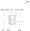
- FIG. 9 it is assumed that light 91 in the reverse direction is incident on the optical isolator element 60 from the first polarizer 62 side. The light 91 in the reverse direction is blocked by the second polarizer 63, but the reflected light 92 partially reflected by the interface 63 a having a high metal particle density of the second polarizer 63 is again the metal particles of the first polarizer 62.
- the light is reflected by the high-density interface 62a and is emitted as the outgoing light 93 from the second polarizer 63 side to the outside. Since a part of the light in the reverse direction is transmitted through the optical isolator element 60 in this way, there arises a problem that the isolation characteristic is deteriorated.
- an object of the present invention is to provide an optical isolator element that is less likely to be deteriorated in isolation characteristics and can be easily thinned.
- An optical isolator element includes a Faraday rotator that rotates a polarization plane of light, a first polarizer disposed on one side of the Faraday rotator, and the other side of the Faraday rotator. And a second polarizer disposed on the side.
- the first polarizer and the second polarizer are light absorption polarizers having a metal particle layer in which metal particles are distributed.
- the second polarizer has a metal particle layer in which metal particles are distributed at a density greater than the density of the metal particles distributed in the metal particle layer of the first polarizer.
- An optical isolator element includes a light absorption type first, second, and third polarizer having metal particle layers in which metal particles are distributed, and the first and second polarizers.
- a first Faraday rotator disposed between and a second Faraday rotator disposed between the second and third polarizers are arranged in a line.
- the metal particle density distributed in the metal particle layer of one of the first, second, and third polarizers is distributed in the metal particle layer of another polarizer. It is characterized by being larger.
- An optical isolator element includes a light absorption type first, second, and third polarizer having metal particle layers in which metal particles are distributed, and the first and second polarizers.
- a first Faraday rotator disposed between and a second Faraday rotator disposed between the second and third polarizers are arranged in a line.
- the metal particle density distributed in the metal particle layer of the first and third polarizers is greater than the metal particle density distributed in the metal particle layer of the second polarizer.
- An optical module includes a light emitting element therein, and any one of the above optical isolator elements is inserted in an optical path of an optical signal emitted from the light emitting element. To do.
- the metal particle density of the metal particle layer distributed in one of the polarizers facing each other via the Faraday rotator is distributed in the other polarizer.
- FIG. 3 is a schematic view schematically showing an example of a type A absorption polarizer.
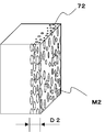
- FIG. 6 is a perspective view schematically showing an example of a type B absorption polarizer.
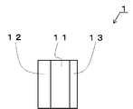
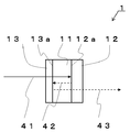
- FIG. 1 shows an optical isolator 1 according to an embodiment of the present invention.
- the optical isolator 1 has a structure in which a first polarizer 12 and a second polarizer 13 are arranged on one and the other of the Faraday rotator 11.
- Each of the elements 11, 12, and 13 is a plate having a constant thickness and is arranged in parallel.
- the Faraday rotator 11 and the first polarizer 12 and the second polarizer 13 disposed on both sides of the Faraday rotator 11 are integrally bonded and fixed using, for example, an adhesive.
- An adhesive having the same refractive index as that of the elements 11, 12, and 13 is suitable.
- an acrylic or epoxy thermosetting type, UV curable type, or a combination type of both types is used. Things are used. Of course, it may be arranged via another transparent medium that is not an adhesive, such as air.
- a bismuth (Bi) -substituted garnet or YIG garnet to which terbium (Tb), gadolinium (Gd) or holmium (Ho) is added, or a self-bias type that does not require a magnet is used.
- Tb terbium
- Gd gadolinium
- Ho holmium
- an antireflection film composed of a multilayer film such as titania (TiO 2 ) and silica (SiO 2 ) or tantalum pentoxide (Ta 2 O 5 ) and SiO 2 is formed. May be.
- the reflection of light on the surface of the Faraday rotator 11 can be reduced to a reflection amount of 0.2% or less.
- the thickness of the Faraday rotator 11 is adjusted such that the Faraday rotation angle is 45 °, for example, in accordance with the type of material of the Faraday rotator 11 and the wavelength of light used. Specifically, it has a thickness of 0.2 to 0.5 mm, although it varies depending on the type of material and the wavelength used. And it arrange
- the first polarizer 12 of the optical isolator element 1 has a density of metal particles distributed in the metal particle layer included in the surface or inner layer of the second polarizer 13 in the density of metal particles distributed in the metal particle layer included in the surface or inner layer. It is a type A polarizer smaller than the density.
- the second polarizer 13 has the density of the metal particles distributed in the metal particle layer included in the surface or inner layer of the first polarizer 12 in the density of the metal particles distributed in the metal particle layer included in the surface or inner layer. It is a type B polarizer larger than the density.
- FIG. 1 shows an example in which the first polarizer 11 is arranged on the left side of the Faraday rotator 11 and the second polarizer 13 is arranged on the right side, the same is true if they are arranged in reverse.
- the optical isolator element 1 includes a Faraday rotator 11 having a type A polarizer disposed on one surface and a type B polarizer disposed on the other surface.
- the type A and type B polarizers are arranged to face each other with the Faraday rotator 11 in between.
- FIG. 10A is a perspective view schematically showing a type A polarizer
- FIG. 10B is a perspective view schematically showing a type B polarizer.
- metal particles M1 and M2 are scattered inside the polarizer near the surface. Some of the metal particles M1 and M2 have an elongated shape having a major axis in one axis direction of the polarizer (the vertical direction in FIGS. 10A and 10B).
- metal particles M1 are scattered in the metal particle layer 71 having a depth D1
- the type B polarizer shown in FIG. Particles M2 are scattered.
- the metal particle layers 71 and 72 may be formed inside the polarizer.
- the density of the metal particles M1 and M2 is highest inside the polarizer.
- the depths D1 and D2 of the metal particle layers 71 and 72 are defined by the thicknesses of the metal particle layers 71 and 72 in which the presence of the metal particles M1 and M2 is confirmed by cross-sectional observation using a TEM.
- the thickness D2 of the metal particle layer 72 distributed on the surface or inner layer of the type B polarizer is 1 ⁇ 2 or less of the thickness D1 of the metal particle layer 71 of the type A polarizer. is there.
- the distribution density of the metal particles M1 distributed on the surface or the inner layer is smaller than that of the type B polarizer, and the distribution thickness D1 of the distributed metal particles M1 is the distribution thickness of the type B polarizer. Thicker than D2.
- a type A polarizer first forms a halide crystal such as copper (Cu), silver (Ag), or cadmium (Cd) in a glass such as quartz glass.
- the glass and halide crystals are softened by heating and stretched in one direction together with the glass, and are heated and reduced in a hydrogen atmosphere to deposit metal particles M1 on the glass surface.
- the halide crystals become acicular crystals that are partially oriented in one direction, and are reduced to form acicular metal particles M1.
- metal particles M1 formed on the halide crystal surface or inside the halide crystal are distributed to a depth of 20 ⁇ m or more from the polarizer surface.
- the reflectance can be made less than 0.5%.
- the distribution depth D1 of the metal particles M1 is deep, it is not suitable for the purpose of producing a thin polarizer.
- the thickness of the type A polarizer is in the range of 0.1 to 1 mm.
- the metal particles M2 are embedded in the surface of a base material such as glass by sputtering and the like, and this is heated and stretched in one direction together with the glass, whereby the needle-like metal particles M2 are oriented in one direction. It exhibits a polarizing function. There is a feature that no halide is contained in the glass, and the metal particles M2 are distributed in a range of 10 ⁇ m at most from the glass surface.
- the metal particles M2 are made of a metal such as copper or silver as in the case of the type A polarizer.
- the type B polarizer has a high refractive index due to the high density of the metal particles M2 near the surface of the base material with respect to the light in the cutoff polarization direction (having the polarization plane in the cutoff direction), and the anti-air layer
- the reflection of the polarizer occurs about 4 to 15%.
- the metal particles M2 transmit the light.
- the refractive index is a constant value similar to that of the base glass, and the reflectance is a stable reflectance of about 4% with respect to the air layer.
- the extinction ratio of the polarizer is deteriorated, so that it is not suitable as a polarizer used in the isolator element 1.
- This type B polarizer is suitable for the purpose of producing a thin polarizer because the metal particles M2 are concentrated on the surface of the base material. Specifically, the thickness of the type B polarizer can be produced in the range of 0.03 ⁇ m to 1 mm.
- the distribution density of the metal particles M1 and M2 can be confirmed by observing a thin section of the polarizer with a TEM.
- the observed metal particles M1 and M2 can specify the type of metal using EDS (energy dispersive X-ray analysis).
- a depth at which the metal particles M1 and M2 are not observed from the surface of the base material is defined as a distribution depth. Since the type B polarizer does not contain metal atoms inside the base material, the distribution depth can also be examined by an elemental analysis instrument such as XPS (X-ray photoelectron spectroscopy).
- XPS X-ray photoelectron spectroscopy
- the type A polarizer has the feature that the density of the metal particles is low overall, but the depth of distribution is deep, and it is distributed to around 50 ⁇ m.
- the type B polarizer has a feature that the distribution density in the vicinity of the surface is high but the distribution depth is shallow, and the metal particles are concentrated in the vicinity of the surface having a depth of 10 ⁇ m at most.
- layers containing metal particles are formed on both surfaces of the polarizer.
- since the distribution depth of the metal particles is deep, it is more difficult to make the polarizer thinner when the metal particle layer is formed on both sides.
- the distribution depth of the metal particles is 1 ⁇ 2 or less that of type A. Then, by combining the two types of polarizers into the optical isolator element 1, it is possible to improve the degradation of isolation characteristics. This will be described with reference to FIG.
- FIG. 4A shows a type A polarizer used for the first polarizer 12 and a type B polarizer used for the second polarizer 13.
- incident light 41 in the opposite direction is incident, a part of the incident light 41 is reflected by the high refractive index metal particle layer 13 a of the second polarizer 13, and reflected light 42 is generated.
- the first polarizer 12 does not have a high refractive index layer, the reflected light 43 from the first polarizer 12 hardly occurs.
- the reflection of the surface 12a of the first polarizer 12 of type A is 0.5% or less, and there is little possibility that the reflected light 43 that affects the isolation characteristic is generated.
- the reflected light 42 travels back and forth within the Faraday rotator 11, so that most of the reflected light 42 is absorbed by the first polarizer 12.
- the type A first polarizer 12 does not have a high refractive index layer. Incident light 41 hardly generates reflected light 42 in the metal particle layer 12 a of the first polarizer 12. Therefore, even if the reflected light 42 is reflected by the metal particle layer 12a of the second polarizer 12, the reflected light 43 is very small and there is little possibility of degrading the isolation characteristics.
- Such an optical isolator element 1 according to an embodiment of the present invention can be used in a stacked manner, and the isolation characteristics can be further improved.
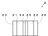
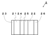
- An example of such an optical isolator 2 used in a stacked manner will be described with reference to FIGS. 2A, 2B, and 2C.
- the optical isolator element 2 in FIG. 2A is an example in which type B polarizers are used for the first polarizer 23 and the fourth polarizer 26, and type A polarizers are used for the second polarizer 24 and the third polarizer 25. Indicates.
- the optical isolator element 2 in FIG. 2B is an example in which type A polarizers are used for the first polarizer 23 and the fourth polarizer 26, and type B polarizers are used for the second polarizer 24 and the third polarizer 25. Indicates.
- the optical isolator element 2 in FIG. 2C is an example in which a type B polarizer is used for the first polarizer 23, and a type A polarizer is used for the second polarizer 24, the third polarizer 25, and the fourth polarizer 26. Is shown.
- the conventional optical isolator element 1 is used as shown in FIG. 2C. It is possible to overlap and use optical isolator elements using the type A of the mold on both sides.
- the second polarizer 24 and the third polarizer 25 need to be overlapped with the same direction so that the polarization directions are the same.
- 2A, 2B, and 2C show an example in which the optical isolators of FIG. 1 are combined in two stages, but three or more stages may be combined.
- 2A, FIG. 2B, and FIG. 2C do not show all examples in which the optical isolators of FIG. 1 are combined in multiple layers, but there are no restrictions on the way of stacking, and other ways of stacking are possible.
- the first polarizer 23 and the third polarizer 25 may be type B polarizers
- the second polarizer 24 and the fourth polarizer 26 may be type A polarizers.
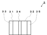
- the optical isolator element 3 of the present embodiment uses two Faraday rotators, and the isolation is lower than that of the optical isolator element 2 shown in FIGS. 2A, 2B, and 2C. As compared with the optical isolator element 1 shown in FIG. 1, sufficiently high isolation characteristics can be obtained, and there is an advantage that the optical isolator element 2 shown in FIGS. 2A, 2B, and 2C can be made thinner.
- a first polarizer 33, a first Faraday rotator 31, a second polarizer 34, a second Faraday rotator 32, and a third polarizer 35 are arranged in a line, and these are arranged.
- the structure is fixed by stacking.
- Each element 33, 31, 34, 32, 35 is arranged in parallel.
- the first Faraday rotator 31 and the second Faraday rotator 32 can be the same as the Faraday rotator 11 shown in FIG.
- the second polarizer 34 is arranged at 45 ° with respect to the transmission polarization plane of the first polarizer 33 with respect to the forward light
- the third polarizer 35 is the transmission polarization plane of the second polarizer 34. It arrange
- FIG. 3A shows an example in which a type B polarizer is used for the first polarizer 33 and the third polarizer 35, and a type A polarizer is used for the second polarizer 34.
- the optical isolator element 2 in FIG. 3B shows an example in which a type A polarizer is used for the first polarizer 33 and the third polarizer 35 and a type B polarizer is used for the second polarizer 34.
- the optical isolator element 3 either of the examples of FIGS. 3A and 3B can be used.
- the type B polarizer is arranged in the second polarizer 34 in the example of FIG. 3B.
- the type B polarizer is limited to the second polarizer 34. It may be used for any one of the first, second, and third polarizers 33, 34, and 35. As described above, any one of the first, second, and third polarizers 33, 34, and 35 may be a type B polarizer having a high metal particle density distributed in the metal particle layer.
- FIG. 3A the configuration shown in FIG. 3A is desirable because there is a possibility that the optical isolator element 3 can be made thinner.
- the isolation characteristics of these optical isolator elements 3 will be described with reference to FIG.
- FIG. 5A shows a case where the optical isolator element 3 of FIG. 3A is used.
- reflected light 42 reflected by the metal particle layer 35 a of the type B third polarizer 35 is generated.
- the reflected light 42 is hardly reflected by the metal particle layer 34a because the polarizer 34 is a type A polarizer. Therefore, the reflected light 43 reflected by the metal particle layer 34a of the second polarizer 34 is small.
- the reflected light 42 reciprocates in the second Faraday rotator 32, the polarization direction is rotated by 90 ° when it returns to the second polarizer 34, and passes through the second polarizer 34.
- the light reaching the first polarizer 33 is small. Therefore, the reflected light 43 emitted from the optical isolator element 3 does not deteriorate the isolation characteristics.
- FIG. 5B shows the case where the optical isolator element 3 of FIG. 3B is used.
- the incident light 41 in the reverse direction is hardly reflected by the metal particle layer 35a because the third polarizer 35 is a type A polarizer, and the reflected light 42 is small.
- the reflected light 44 generated on the surface of the second polarizer 34 is hardly reflected by the first polarizer 33 because the first polarizer 33 is a type A polarizer, and the reflected light 45 is small. Become. Therefore, the reflected light 44 and the reflected light 45 are small and do not deteriorate the isolation characteristics.
- the type B polarizer is used for the second polarizer 34, but the same effect can be obtained even when the type B polarizer is used for the first polarizer 33 or the third polarizer 35. it can.
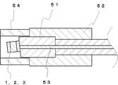
- FIG. 6 is a cross-sectional view showing an example in which an optical fiber holding component with an optical isolator element that constitutes a part of an optical module is configured using the optical isolator elements 1, 2, and 3.
- this optical fiber holding component with optical isolator elements 1, 2, and 3 a ferrule 51 that holds an optical fiber 53 is held by a holding member 52.
- the tip surface of the ferrule 51 is subjected to oblique mirror polishing with respect to the optical axis.
- One of the optical isolator elements 1, 2, 3 is fixed to the front end surface of the ferrule 51 with an adhesive or the like.
- optical isolators 1 and 2 are placed in the optical path of an optical signal emitted from the light emitting element. , 3 are inserted to form an optical module.
- Reference numeral 54 denotes a magnet disposed outside the optical isolators 1, 2, 3.
- the arrangement of the optical isolator element 1 is used for the optical module. It is better to select according to the application.
- the optical isolator 1 is preferably arranged so that the type A polarizer 12 is provided on the tip surface of the ferrule 51 and the type B polarizer 13 is provided on the opposite side.
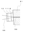
- the condensed beam 55 from the light emitting element is set so as to be focused near the tip of the optical fiber 53.
- the optical module is a pump laser module or the like used for an optical fiber amplifier, and the light source output is a large output light of several tens mW to several hundred mW class, the light beam transmitted through the type B second polarizer 13 having a high metal particle density
- the optical isolator element 1 it is preferable to arrange the optical isolator element 1 so that the diameter becomes larger than the light beam diameter of the type A first polarizer 12 having a small metal particle density.
- the light emitting element side so that the second polarizer 13 of type B and the tip surface side of the ferrule 51 become the first polarizer 12 of type A.
- the thickness of the metal particle layer is thinner than type A, and the second polarizer 13 of type B, which has low light resistance, is arranged on the beam diameter side where the energy density of the beam is small. It is advantageous.
- the reflected return light returned from the ferrule 51 side is incident on the first polarizer 12 with a beam diameter 55 that is about the mode field diameter of the optical fiber 53.
- the beam diameter increases and increases, so that the energy density of the beam in the second polarizer 13 is smaller than the density in the first polarizer 12.
- the type B polarizer has a high density of surface metal particles, and the light is absorbed by the surface metal particle layer and tends to be locally heated as compared with type A, and has low light resistance. For this reason, it is better to use a type B polarizer for the second polarizer 13 on the side where the beam diameter is increased.
- a type B polarizer is preferably arranged.
- the optical fiber holding component has been described.
- the type B is also set to have a lower beam energy density. The light resistance can be improved by arranging the polarizers.
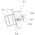
- the optical isolator 1 is arranged on the tip surface of the ferrule 51 as shown in FIG. It is preferable that the second polarizer 13 for B is the first polarizer 12 for type A on the opposite side.
- the light component in the blocking polarization direction is once absorbed by the metal particle layer of the polarizer and converted into heat, but part of it is re-radiated as heat radiation light 57. Is done. Since the radiation direction at this time extends over a wide range centering on the normal direction of the polarizer, if a part of the radiation direction is coupled to the optical fiber 53 again, it becomes noise to the optical signal.
- the second polarizer 13 is a type B polarizer
- the reflected return light 56 returned from the ferrule 51 side a part of the light component in the blocking polarization direction is reflected by the metal particle layer 13a having a high refractive index.
- the reflected light 58 is obtained. Since the reflection angle ⁇ at this time is equal to the incident angle ⁇ to the second polarizer 13, it has a large angle with respect to the optical fiber 53. Therefore, it is difficult for the reflected light 58 to be coupled to the optical fiber 53.
- the light component in the blocking polarization direction that has not been reflected is partially radiated as thermal radiation 57 after being absorbed by the metal particle layer, but is reflected as reflected light 58 by the second polarizer 13. Since the light absorbed by the metal particles is reduced, the emitted light 57 generated by the absorption is also reduced. Therefore, the intensity of the light recombined with the optical fiber 53 is reduced, and the noise component for the optical signal is also reduced.
- interval of the optical fiber 53 and the metal particle layer 13a spreads by arrange
- the optical fiber holding part with an optical isolator element shown in FIG. 6 When the optical fiber holding part with an optical isolator element shown in FIG. 6 is configured, if the optical isolator elements 1, 2, and 3 are fixed to the end face of the optical fiber 53 that becomes the focal point of the condensed beam in this way, a semiconductor laser or the like Since the light emitted from the light emitting element (not shown) is condensed through a lens (not shown) and the optical isolator elements 1, 2, and 3 are installed in a place where the spot diameter of the light is reduced, the optical isolator There is an advantage that the size of the elements 1, 2 and 3 can be reduced. If the thin optical isolator elements 1, 2, and 3 according to the embodiment of the present invention are used, it is possible to provide an optical fiber holding component that is smaller and has excellent isolation characteristics.
- optical isolator element 3 shown in FIG. 3A was produced by the following procedure.
- a Faraday rotator having a thickness of 0.45 mm made of bismuth-substituted garnet ((BiR) 3 Fe 5 O 12 ) was used as the first Faraday rotator 31 and the second Faraday rotator 32.
- a type A polarizer was used as the second polarizer 34
- a type B polarizer was used as the first polarizer 33 and the third polarizer 35.
- a SiO 2 + B 2 O 3 glass base material was used, and a silver halide crystal formed in the glass was stretched and oriented while being heated, and reduced in a hydrogen atmosphere. The thing of 200 micrometers was used.
- the metal particles (silver particles) deposited near the surface had a distribution depth of 50 ⁇ m.
- a SiO 2 + B 2 O 3 glass base material was used, and the one having a thickness of 80 ⁇ m produced by heating and stretching silver particles formed in the glass by sputtering was used.
- the distribution depth of the silver particles near the surface was 5 ⁇ m.
- Comparative Example 1 a conventional optical isolator element was produced.
- the first Faraday rotator and the second Faraday rotator are the same as the Faraday rotators 31 and 32 described above, and the second polarizer 34 described above is used as the first polarizer, the second polarizer, and the third polarizer.
- the same type A polarizer was used. This was cut into a size of 0.5 mm ⁇ 0.6 mm by a dicer to produce a conventional optical isolator element.
- Comparative Example 2 a first type polarizer, a second polarizer, and a third polarizer were manufactured using the same type B polarizer as the first polarizer 33 described above.
- the thickness and isolation characteristics of the optical isolator element 2 and the optical isolator elements of Comparative Examples 1 and 2 were measured. Isolation characteristics are measured by inserting each optical isolator element in a direction opposite to the light transmission direction in a collimator optical system having a wavelength of 1550 nm and a beam diameter of 0.3 mm, and measuring the output light intensity with a power meter. Asked. Each evaluation was performed one by one. The results are shown in Table 1.
- the comparative example 1 has a thickness of 1.508 mm and an isolation characteristic of 61.8 dB
- the comparative example 2 has a thickness of 1.145 mm and an isolation characteristic of 19 dB.
- the thickness is 1.266 mm
- the isolation characteristic is 62.3 dB
- the isolation characteristic is not inferior to that of the comparative example 1 and is confirmed to be significantly improved with respect to the comparative example 2. did it. It was also recognized that miniaturization could be achieved.
- the optical isolator element 3 according to each embodiment of the present invention, the light absorption type first polarizer 33, the second polarizer 34, the third polarizer 35 arranged in a row, A first Faraday rotator 31 disposed between the first polarizer 33 and the second polarizer 34, and a second Faraday rotator 32 disposed between the second polarizer 34 and the third polarizer 35.
- the isolation characteristic is improved. It was found that an isolator element 3 that does not deteriorate is obtained. This also makes it possible to reduce the size of the isolator element 3.
Landscapes
- Physics & Mathematics (AREA)
- Nonlinear Science (AREA)
- Engineering & Computer Science (AREA)
- Power Engineering (AREA)
- General Physics & Mathematics (AREA)
- Optics & Photonics (AREA)
- Polarising Elements (AREA)
Abstract
Description

11:ファラデー回転子
31:第1ファラデー回転子
32:第2ファラデー回転子
12,33:第1偏光子
13,34:第2偏光子
35:第3偏光子
51:フェルール
52:キャピラリ
53:光ファイバ
54:磁石
Claims (18)
- 光の偏光面を回転させるファラデー回転子と、該ファラデー回転子の一方面側に配置され、金属粒子が分布する金属粒子層を有する第1偏光子と、前記ファラデー回転子の他方面側に配置され、前記第1偏光子の金属粒子層に分布する金属粒子の密度より大きい密度で金属粒子が分布する金属粒子層を有する第2偏光子とを備えたことを特徴とする光アイソレータ素子。
- 前記第1偏光子の前記金属粒子層の厚みが前記第2偏光子の前記金属粒子層の厚みより厚いことを特徴とする請求項1記載の光アイソレータ素子。
- 前記第1偏光子の前記金属粒子層の厚みが前記第2偏光子の前記金属粒子層の厚みの2倍以上であることを特徴とする請求項1記載の光アイソレータ素子。
- 前記第1偏光子は、透明基板上に物理的蒸着法により誘電体層と金属粒子層とを蒸着し、基板を延伸させることによって前記金属粒子層に含まれる金属粒子を細長い形状に成形した偏光子であり、前記第2偏光子は、ハロゲン化金属を含むガラス基材の表面近くにハロゲン化金属を還元させて形成された金属粒子を、基板を延伸させることによって細長い形状に成形した偏光子であることを特徴とする請求項1記載の光アイソレータ素子。
- 請求項1記載の光アイソレータ素子を複数枚重ねたことを特徴とする光アイソレータ素子。
- 一列に並べて配置され、金属粒子が分布する金属粒子層を有する光吸収型の第1,第2,第3偏光子と、前記第1および第2偏光子の間に配置された第1ファラデー回転子と、前記第2および第3偏光子の間に配置された第2ファラデー回転子とを備えた光アイソレータ素子であって、前記第1,第2,第3偏光子のうち、いずれか一枚の偏光子の前記金属粒子層に分布する金属粒子密度が他の偏光子の前記金属粒子層に分布する金属粒子密度より大きいことを特徴とする光アイソレータ素子。
- 前記第1,第2,第3偏光子のうち、いずれか一枚の偏光子の前記金属粒子層の厚みが他の偏光子の前記金属粒子層の厚みより薄いことを特徴とする請求項6記載の光アイソレータ素子。
- 前記第1,第2,第3偏光子のうち、いずれか一枚の偏光子の前記金属粒子層の厚みが他の偏光子の前記金属粒子層の厚みの1/2以下であることを特徴とする請求項6記載の光アイソレータ素子。
- 前記第1,第2,第3偏光子のうち、いずれか一枚の偏光子は、透明基板上に物理的蒸着方法により誘電体層と金属粒子層とを蒸着し、基板を延伸させることによって前記金属粒子層に含まれる金属粒子を細長い形状に成形した偏光子であり、他の偏光子は、ハロゲン化金属を含むガラス基材の表面近くにハロゲン化金属を還元させて形成された金属粒子を、基板を延伸させることによって細長い形状に成形した偏光子であることを特徴とする請求項6記載の光アイソレータ素子。
- 一列に並べて配置され、金属粒子が分布する金属粒子層を有する光吸収型の第1,第2,第3偏光子と、前記第1および第2偏光子の間に配置された第1ファラデー回転子と、前記第2および第3偏光子の間に配置された第2ファラデー回転子とを備えた光アイソレータ素子であって、前記第1および第3偏光子の前記金属粒子層に分布する金属粒子密度が、前記第2偏光子の前記金属粒子層に分布する金属粒子密度より大きいことを特徴とする光アイソレータ素子。
- 前記第1および第3偏光子の前記金属粒子層の厚みが前記第2偏光子の前記金属粒子層の厚みより薄いことを特徴とする請求項10記載の光アイソレータ素子。
- 前記第1および第3偏光子の前記金属粒子層の厚みが前記第2偏光子の前記金属粒子層の厚みの1/2以下であることを特徴とする請求項10記載の光アイソレータ素子。
- 前記第1および第3偏光子は、透明基板上に物理的蒸着方法により誘電体層と金属粒子層とを蒸着し、基板を延伸させることによって前記金属粒子層に含まれる金属粒子を細長い形状に成形した偏光子であり、前記第2偏光子は、ハロゲン化金属を含むガラス基材の表面近くにハロゲン化金属を還元させて形成された金属粒子を、基板を延伸させることによって細長い形状に成形した偏光子であることを特徴とする請求項10記載の光アイソレータ素子。
- 内部に発光素子を備え、前記発光素子から出射された光信号の光路中に請求項1記載の光アイソレータ素子が挿入されていることを特徴とする光モジュール。
- 前記発光素子から出射された集光ビームの途中に挿入され、前記第1偏光子を透過する光ビーム径が、前記第2偏光子を透過する光ビーム径に対して大きくなるように前記光アイソレータ素子が配置されていることを特徴とする請求項14記載の光モジュール。
- 内部に発光素子を備え、前記発光素子から出射された光信号の光路中に請求項6記載の光アイソレータ素子が挿入されていることを特徴とする光モジュール。
- 前記発光素子から出射された集光ビームの途中に挿入され、前記金属粒子層の金属粒子密度が大きい偏光子を透過する光ビーム径が、金属粒子密度が小さい偏光子を透過する光ビーム径に対して大きくなるように前記光アイソレータ素子が配置されていることを特徴とする請求項16記載の光モジュール。
- 内部に発光素子を備え、前記発光素子から出射された光信号の光路中に請求項10記載の光アイソレータ素子が挿入されていることを特徴とする光モジュール。
Priority Applications (3)
| Application Number | Priority Date | Filing Date | Title |
|---|---|---|---|
| JP2011506029A JP5188623B2 (ja) | 2009-03-25 | 2010-03-19 | 光アイソレータ素子およびこれを用いた光モジュール |
| US13/259,133 US8830578B2 (en) | 2009-03-25 | 2010-03-19 | Optical isolator element and optical module using the same |
| CN201080013291.8A CN102362210B (zh) | 2009-03-25 | 2010-03-19 | 光隔离器件及使用了该光隔离器件的光模块 |
Applications Claiming Priority (4)
| Application Number | Priority Date | Filing Date | Title |
|---|---|---|---|
| JP2009-073637 | 2009-03-25 | ||
| JP2009073637 | 2009-03-25 | ||
| JP2009-249355 | 2009-10-29 | ||
| JP2009249355 | 2009-10-29 |
Publications (1)
| Publication Number | Publication Date |
|---|---|
| WO2010110219A1 true WO2010110219A1 (ja) | 2010-09-30 |
Family
ID=42780914
Family Applications (1)
| Application Number | Title | Priority Date | Filing Date |
|---|---|---|---|
| PCT/JP2010/054849 Ceased WO2010110219A1 (ja) | 2009-03-25 | 2010-03-19 | 光アイソレータ素子およびこれを用いた光モジュール |
Country Status (4)
| Country | Link |
|---|---|
| US (1) | US8830578B2 (ja) |
| JP (1) | JP5188623B2 (ja) |
| CN (1) | CN102362210B (ja) |
| WO (1) | WO2010110219A1 (ja) |
Cited By (1)
| Publication number | Priority date | Publication date | Assignee | Title |
|---|---|---|---|---|
| CN102736154A (zh) * | 2011-04-12 | 2012-10-17 | 夏普株式会社 | 光学滤波器、显示单元及显示装置 |
Families Citing this family (1)
| Publication number | Priority date | Publication date | Assignee | Title |
|---|---|---|---|---|
| US9581742B2 (en) * | 2012-11-20 | 2017-02-28 | Corning Incorporated | Monolithic, linear glass polarizer and attenuator |
Citations (5)
| Publication number | Priority date | Publication date | Assignee | Title |
|---|---|---|---|---|
| JP2000284226A (ja) * | 1999-03-31 | 2000-10-13 | Kyocera Corp | 光アイソレータ |
| JP2001051235A (ja) * | 1999-08-11 | 2001-02-23 | Shin Etsu Chem Co Ltd | 光アイソレータ用又は光磁界センサ用光学部品及びその製造方法並びに光ファイバ接続型光アイソレータ |
| JP2006208710A (ja) * | 2005-01-27 | 2006-08-10 | Kyocera Corp | 光アイソレータ素子及びその製造方法並びに光アイソレータ付きファイバ |
| JP2006284769A (ja) * | 2005-03-31 | 2006-10-19 | Kyocera Corp | 光アイソレータ素子およびその製造方法 |
| JP2008299329A (ja) * | 2007-05-29 | 2008-12-11 | Hoya Candeo Optronics株式会社 | 偏光ガラスの製造方法 |
Family Cites Families (9)
| Publication number | Priority date | Publication date | Assignee | Title |
|---|---|---|---|---|
| US6313947B1 (en) * | 1991-10-14 | 2001-11-06 | Hoya Corporation | Light polarizing glass containing copper particles and process for preparation thereof |
| US5517356A (en) | 1993-12-15 | 1996-05-14 | Corning Incorporated | Glass polarizer for visible light |
| EP0719742B1 (en) * | 1994-12-27 | 1998-04-08 | Hoya Corporation | Polarizing glass and production process thereof |
| DE69625642T2 (de) * | 1995-05-23 | 2003-05-28 | Kyocera Corp., Kyoto | Methode zu Herstellung eines optischen Polarisators |
| JPH09178939A (ja) | 1995-12-26 | 1997-07-11 | Kyocera Corp | 偏光子およびその製造方法 |
| US5999315A (en) * | 1996-04-26 | 1999-12-07 | Kyocera Corporation | Polarizer and a production method thereof and an optical isolator |
| US6806990B2 (en) * | 2001-11-22 | 2004-10-19 | Shin-Etsu Chemical Co., Ltd. | Optical device and method for producing optical device |
| US6563639B1 (en) * | 2002-01-24 | 2003-05-13 | Corning Incorporated | Polarizing glasses |
| JP4402728B2 (ja) * | 2008-04-21 | 2010-01-20 | Hoya Candeo Optronics株式会社 | 偏光ガラス、光アイソレーターおよび偏光ガラスの製造方法 |
-
2010
- 2010-03-19 US US13/259,133 patent/US8830578B2/en not_active Expired - Fee Related
- 2010-03-19 WO PCT/JP2010/054849 patent/WO2010110219A1/ja not_active Ceased
- 2010-03-19 CN CN201080013291.8A patent/CN102362210B/zh not_active Expired - Fee Related
- 2010-03-19 JP JP2011506029A patent/JP5188623B2/ja not_active Expired - Fee Related
Patent Citations (5)
| Publication number | Priority date | Publication date | Assignee | Title |
|---|---|---|---|---|
| JP2000284226A (ja) * | 1999-03-31 | 2000-10-13 | Kyocera Corp | 光アイソレータ |
| JP2001051235A (ja) * | 1999-08-11 | 2001-02-23 | Shin Etsu Chem Co Ltd | 光アイソレータ用又は光磁界センサ用光学部品及びその製造方法並びに光ファイバ接続型光アイソレータ |
| JP2006208710A (ja) * | 2005-01-27 | 2006-08-10 | Kyocera Corp | 光アイソレータ素子及びその製造方法並びに光アイソレータ付きファイバ |
| JP2006284769A (ja) * | 2005-03-31 | 2006-10-19 | Kyocera Corp | 光アイソレータ素子およびその製造方法 |
| JP2008299329A (ja) * | 2007-05-29 | 2008-12-11 | Hoya Candeo Optronics株式会社 | 偏光ガラスの製造方法 |
Cited By (1)
| Publication number | Priority date | Publication date | Assignee | Title |
|---|---|---|---|---|
| CN102736154A (zh) * | 2011-04-12 | 2012-10-17 | 夏普株式会社 | 光学滤波器、显示单元及显示装置 |
Also Published As
| Publication number | Publication date |
|---|---|
| US20120134021A1 (en) | 2012-05-31 |
| JPWO2010110219A1 (ja) | 2012-09-27 |
| JP5188623B2 (ja) | 2013-04-24 |
| CN102362210B (zh) | 2013-09-25 |
| CN102362210A (zh) | 2012-02-22 |
| US8830578B2 (en) | 2014-09-09 |
Similar Documents
| Publication | Publication Date | Title |
|---|---|---|
| US6813076B2 (en) | Faraday rotator, optical isolator, polarizer, and diamond-like carbon thin film | |
| US8115998B2 (en) | In-line optical isolator | |
| CN101939671B (zh) | 偏光玻璃、光隔离器及偏光玻璃的制造方法 | |
| JP5188623B2 (ja) | 光アイソレータ素子およびこれを用いた光モジュール | |
| KR20000015885A (ko) | 광 아이솔레이터 | |
| JP2000310750A (ja) | 光アイソレータ及びそれを用いた光モジュール | |
| JP2008310068A (ja) | インライン光アイソレータ | |
| JP3784198B2 (ja) | 光アイソレータ | |
| JP7654485B2 (ja) | 光学素子及びその製造方法並びに光アイソレータ、光伝送装置 | |
| JP2000180789A (ja) | 光アイソレータ | |
| JP7764360B2 (ja) | 光アイソレータ | |
| JP4628054B2 (ja) | 光アイソレータ | |
| JP2004341076A (ja) | 光アイソレータおよびレーザダイオードモジュール | |
| JP3616349B2 (ja) | 偏光素子付き磁気光学結晶板 | |
| JP2006208710A (ja) | 光アイソレータ素子及びその製造方法並びに光アイソレータ付きファイバ | |
| US20260029673A1 (en) | Optical isolator production method, optical isolator, and polarizing glass | |
| JP2006309190A (ja) | 光アイソレータおよびそれを用いた光モジュール | |
| JP2022006506A (ja) | 光学素子及びその製造方法並びに光アイソレータ、光伝送装置 | |
| CN100529807C (zh) | 偏光片的制造方法 | |
| JP2006284769A (ja) | 光アイソレータ素子およびその製造方法 | |
| JPH11249072A (ja) | 偏光子及びそれを用いた光アイソレータ | |
| JP2018189880A (ja) | 偏光部材及び光アイソレータ | |
| JP2015125374A (ja) | 光アイソレータ素子と光アイソレータ | |
| JP2008003189A (ja) | 光ファイバ一体型光アイソレータ | |
| JP2006064991A (ja) | 光学素子とこれを用いた光モジュール |
Legal Events
| Date | Code | Title | Description |
|---|---|---|---|
| WWE | Wipo information: entry into national phase |
Ref document number: 201080013291.8 Country of ref document: CN |
|
| 121 | Ep: the epo has been informed by wipo that ep was designated in this application |
Ref document number: 10756016 Country of ref document: EP Kind code of ref document: A1 |
|
| WWE | Wipo information: entry into national phase |
Ref document number: 2011506029 Country of ref document: JP |
|
| NENP | Non-entry into the national phase |
Ref country code: DE |
|
| WWE | Wipo information: entry into national phase |
Ref document number: 13259133 Country of ref document: US |
|
| 122 | Ep: pct application non-entry in european phase |
Ref document number: 10756016 Country of ref document: EP Kind code of ref document: A1 |