WO2010110122A1 - アクチュエータ、駆動装置、および撮像装置 - Google Patents
アクチュエータ、駆動装置、および撮像装置 Download PDFInfo
- Publication number
- WO2010110122A1 WO2010110122A1 PCT/JP2010/054434 JP2010054434W WO2010110122A1 WO 2010110122 A1 WO2010110122 A1 WO 2010110122A1 JP 2010054434 W JP2010054434 W JP 2010054434W WO 2010110122 A1 WO2010110122 A1 WO 2010110122A1
- Authority
- WO
- WIPO (PCT)
- Prior art keywords
- layer
- actuator
- lens group
- movable
- heater
- Prior art date
- Legal status (The legal status is an assumption and is not a legal conclusion. Google has not performed a legal analysis and makes no representation as to the accuracy of the status listed.)
- Ceased
Links
Images











Classifications
-
- F—MECHANICAL ENGINEERING; LIGHTING; HEATING; WEAPONS; BLASTING
- F03—MACHINES OR ENGINES FOR LIQUIDS; WIND, SPRING, OR WEIGHT MOTORS; PRODUCING MECHANICAL POWER OR A REACTIVE PROPULSIVE THRUST, NOT OTHERWISE PROVIDED FOR
- F03G—SPRING, WEIGHT, INERTIA OR LIKE MOTORS; MECHANICAL-POWER PRODUCING DEVICES OR MECHANISMS, NOT OTHERWISE PROVIDED FOR OR USING ENERGY SOURCES NOT OTHERWISE PROVIDED FOR
- F03G7/00—Mechanical-power-producing mechanisms, not otherwise provided for or using energy sources not otherwise provided for
- F03G7/06—Mechanical-power-producing mechanisms, not otherwise provided for or using energy sources not otherwise provided for using expansion or contraction of bodies due to heating, cooling, moistening, drying or the like
- F03G7/061—Mechanical-power-producing mechanisms, not otherwise provided for or using energy sources not otherwise provided for using expansion or contraction of bodies due to heating, cooling, moistening, drying or the like characterised by the actuating element
- F03G7/0613—Mechanical-power-producing mechanisms, not otherwise provided for or using energy sources not otherwise provided for using expansion or contraction of bodies due to heating, cooling, moistening, drying or the like characterised by the actuating element using layers of different materials joined together, e.g. bimetals
-
- F—MECHANICAL ENGINEERING; LIGHTING; HEATING; WEAPONS; BLASTING
- F03—MACHINES OR ENGINES FOR LIQUIDS; WIND, SPRING, OR WEIGHT MOTORS; PRODUCING MECHANICAL POWER OR A REACTIVE PROPULSIVE THRUST, NOT OTHERWISE PROVIDED FOR
- F03G—SPRING, WEIGHT, INERTIA OR LIKE MOTORS; MECHANICAL-POWER PRODUCING DEVICES OR MECHANISMS, NOT OTHERWISE PROVIDED FOR OR USING ENERGY SOURCES NOT OTHERWISE PROVIDED FOR
- F03G7/00—Mechanical-power-producing mechanisms, not otherwise provided for or using energy sources not otherwise provided for
- F03G7/06—Mechanical-power-producing mechanisms, not otherwise provided for or using energy sources not otherwise provided for using expansion or contraction of bodies due to heating, cooling, moistening, drying or the like
- F03G7/061—Mechanical-power-producing mechanisms, not otherwise provided for or using energy sources not otherwise provided for using expansion or contraction of bodies due to heating, cooling, moistening, drying or the like characterised by the actuating element
- F03G7/0614—Mechanical-power-producing mechanisms, not otherwise provided for or using energy sources not otherwise provided for using expansion or contraction of bodies due to heating, cooling, moistening, drying or the like characterised by the actuating element using shape memory elements
-
- F—MECHANICAL ENGINEERING; LIGHTING; HEATING; WEAPONS; BLASTING
- F03—MACHINES OR ENGINES FOR LIQUIDS; WIND, SPRING, OR WEIGHT MOTORS; PRODUCING MECHANICAL POWER OR A REACTIVE PROPULSIVE THRUST, NOT OTHERWISE PROVIDED FOR
- F03G—SPRING, WEIGHT, INERTIA OR LIKE MOTORS; MECHANICAL-POWER PRODUCING DEVICES OR MECHANISMS, NOT OTHERWISE PROVIDED FOR OR USING ENERGY SOURCES NOT OTHERWISE PROVIDED FOR
- F03G7/00—Mechanical-power-producing mechanisms, not otherwise provided for or using energy sources not otherwise provided for
- F03G7/06—Mechanical-power-producing mechanisms, not otherwise provided for or using energy sources not otherwise provided for using expansion or contraction of bodies due to heating, cooling, moistening, drying or the like
- F03G7/064—Mechanical-power-producing mechanisms, not otherwise provided for or using energy sources not otherwise provided for using expansion or contraction of bodies due to heating, cooling, moistening, drying or the like characterised by its use
-
- F—MECHANICAL ENGINEERING; LIGHTING; HEATING; WEAPONS; BLASTING
- F03—MACHINES OR ENGINES FOR LIQUIDS; WIND, SPRING, OR WEIGHT MOTORS; PRODUCING MECHANICAL POWER OR A REACTIVE PROPULSIVE THRUST, NOT OTHERWISE PROVIDED FOR
- F03G—SPRING, WEIGHT, INERTIA OR LIKE MOTORS; MECHANICAL-POWER PRODUCING DEVICES OR MECHANISMS, NOT OTHERWISE PROVIDED FOR OR USING ENERGY SOURCES NOT OTHERWISE PROVIDED FOR
- F03G7/00—Mechanical-power-producing mechanisms, not otherwise provided for or using energy sources not otherwise provided for
- F03G7/06—Mechanical-power-producing mechanisms, not otherwise provided for or using energy sources not otherwise provided for using expansion or contraction of bodies due to heating, cooling, moistening, drying or the like
- F03G7/066—Actuator control or monitoring
- F03G7/0665—Actuator control or monitoring controlled displacement, e.g. by using a lens positioning actuator
-
- G—PHYSICS
- G02—OPTICS
- G02B—OPTICAL ELEMENTS, SYSTEMS OR APPARATUS
- G02B27/00—Optical systems or apparatus not provided for by any of the groups G02B1/00 - G02B26/00, G02B30/00
- G02B27/0025—Optical systems or apparatus not provided for by any of the groups G02B1/00 - G02B26/00, G02B30/00 for optical correction, e.g. distorsion, aberration
Definitions
- the present invention relates to an actuator, and a driving device and an imaging device using the actuator.
- An actuator for driving an optical system and a mechanical mechanism is essential for the enhancement of the function of such a camera module, and an actuator for realizing a higher function while satisfying the demand for a reduction in size and weight is required.
- actuators using shape memory alloys have attracted attention.
- displacement is generated by expanding and contracting the shape memory alloy by energization heating of the shape memory alloy.
- technique which detects a displacement indirectly by detecting the change of the resistance value by deformation
- the deformation of the shape memory alloy affects both the change in the resistance value of the shape memory alloy and the displacement of the actuator. For this reason, if it is going to give a desired driving force to an actuator, the dimension of a shape memory alloy will be limited. In other words, the dimensions, resistance values, etc. of the shape memory alloy are determined in relation to output characteristics such as driving force and displacement that the actuator wants to have. That is, the degree of freedom in actuator design is greatly limited. And such a problem can become a very big obstruction factor in aiming at size reduction and weight reduction of an actuator.
- the present invention has been made in view of the above problems, and provides an actuator having a configuration capable of controlling displacement and having a high degree of design freedom, and a drive device and an imaging device using the actuator. Objective.
- the actuator according to the first aspect includes a movable part that deforms in response to heat generation, and a control unit that controls a deformation amount of the movable part.
- the movable portion has a structure in which a plurality of portions including a base portion, a force generating portion that generates a force in response to heating, and a heat generating portion that generates heat in response to a current supply are stacked. is doing.
- the said control part controls the deformation amount of the said movable part by controlling the electric current supplied to the said heat generating part based on the electrical resistance of the said heat generating part.
- the actuator according to the second aspect is the actuator according to the first aspect, wherein the heat generating portion is based on the first region between the base portion and the force generating portion, and the force generating portion. As at least one of the second regions located in a direction opposite to the direction in which the base portion exists.
- the actuator according to the third aspect is the actuator according to the first aspect, wherein the force generation part includes a shape memory alloy.
- the actuator according to the fourth aspect is the actuator according to the first aspect, wherein the force generation part has a higher thermal expansion coefficient than the thermal expansion coefficient of the base part.
- the drive device includes the actuator according to the first aspect and a moving object that is moved by deformation of the movable part.
- an imaging apparatus includes the actuator according to the first aspect, an imaging element, and an optical system that guides light from a subject to the imaging element.
- the imaging apparatus at least one of the imaging element and the optical system is moved by deformation of the movable portion.
- the actuator since the portion that generates force in response to heating and the portion that generates heat are provided separately, the displacement can be controlled and the design has a high degree of freedom.
- An actuator can be provided.
- the deformation amount of the movable portion can be controlled with high accuracy.
- the actuator according to the third aspect greatly deforms the movable part with respect to the application of electric current, so that the movable part can be efficiently deformed.
- the actuator according to the fourth aspect can reduce the manufacturing cost.
- the drive device According to the drive device according to the fifth aspect, it is possible to realize a drive device using an actuator having a configuration capable of controlling displacement and having a high degree of design freedom.
- an imaging device using an actuator having a configuration capable of controlling displacement and having a high degree of design freedom is realized.
- FIG. 1 is a schematic diagram showing a schematic configuration of a mobile phone equipped with a camera module according to an embodiment of the present invention.
- FIG. 2 is a schematic cross-sectional view focusing on the first housing according to the embodiment of the present invention.
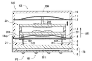
- FIG. 3 is a schematic cross-sectional view of a camera module according to an embodiment of the present invention.
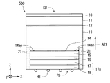
- FIG. 4 is an external view of a camera module according to an embodiment of the present invention as viewed from the side.
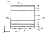
- FIG. 5 is an external view of a camera module according to an embodiment of the present invention as viewed from the side.
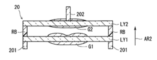
- FIG. 6 is a schematic cross-sectional view of the lens group.
- FIG. 7 is a schematic cross-sectional view of the lens group.
- FIG. 8 is an external view of the first lens component layer as viewed from below.
- FIG. 9 is an external view of the second lens component layer as viewed from above.
- FIG. 10 is a diagram for explaining the shape of the spacer layer.
- FIG. 11 is an external view of the lens position adjustment layer as viewed from above.
- FIG. 12 is an external view of the lens position adjustment layer as viewed from the side.
- FIG. 13 is an external view of the actuator layer as viewed from above.
- FIG. 14 is an external view of the actuator layer as viewed from the side.
- FIG. 15 is a diagram showing the shape of the base layer constituting the actuator layer.
- FIG. 16 is a diagram showing the shape of the actuator element layer that constitutes the actuator layer.
- FIG. 17 is a diagram showing the shape of the insulating layer constituting the actuator layer.
- FIG. 18 is a diagram showing the shape of the heater layer constituting the actuator layer.
- FIG. 19 is a top external view showing a detailed configuration of the actuator layer.
- FIG. 20 is a diagram for explaining an operation example of the movable part.
- FIG. 21 is a diagram for explaining an operation example of the movable part.
- FIG. 22 is an external view of the second parallel spring as viewed from below.
- FIG. 23 is a diagram illustrating a second parallel spring attached to the lens group.
- FIG. 24 is an external view of the first parallel spring as viewed from below.
- FIG. 25 is a diagram illustrating the first parallel spring mounted on the lens group.
- FIG. 26 is a block diagram showing a functional configuration related to autofocus control.
- FIG. 27 is a flowchart showing the manufacturing process of the camera module.
- FIG. 28 is a diagram schematically illustrating a state in which prepared sheets and the like are stacked and joined.
- FIG. 29 is a diagram illustrating an aspect in which an image sensor
- FIG. 1 is a schematic diagram showing a schematic configuration of a mobile phone 100 equipped with a camera module 500 according to an embodiment of the present invention.
- the mobile phone 100 is configured as a foldable mobile phone, and includes a first casing 200, a second casing 300, and a hinge part 400.
- Each of the first casing 200 and the second casing 300 has a plate-like substantially rectangular parallelepiped shape and serves as a casing for storing various electronic members.
- the first casing 200 includes a camera module 500 and a display (not shown)
- the second casing 300 includes a control unit that electrically controls the mobile phone 100, buttons, and the like. And an operation member (not shown).
- the hinge part 400 has connected the 1st housing
- the current supply driver 600, the electric resistance detection unit 700, and the contrast detection unit 800 are mounted on the first casing 200.
- the current supply driver 600 controls supply of current to the heater layer 154 (FIG. 18) of the camera module 500.
- the electrical resistance detector 700 detects electrical resistance in the heater layer 154.
- the contrast detector 800 detects the contrast of the image signal obtained by the image sensor 181 (FIG. 3) of the camera module 500.
- a focusing control unit 310 is mounted on the second casing 300.
- the focus control unit 310 controls the amount of current supplied to the heater layer 154 via the current supply driver 600 in accordance with the input of signals from the electrical resistance detection unit 700 and the contrast detection unit 800, so that the camera module Auto focus control for adjusting the in-focus state of 500 is performed. This autofocus control will be further described later.
- FIG. 2 is a schematic cross-sectional view focusing on the first casing 200 of the mobile phone 100.
- the camera module 500 is a small imaging device, so-called micro camera unit, having an XY cross section of about 5 mm square and a thickness (depth in the Z direction) of about 3 mm. (MCU).
- FIG. 3 is a schematic cross-sectional view of the camera module 500, and the direction indicated by the arrow AR1 in FIG. 3 corresponds to the + Z direction.
- an arrow AR ⁇ b> 1 indicating a direction corresponding to the + Z direction is appropriately attached in order to clarify the orientation relationship.
- 4 and 5 are side views of the camera module 500 as viewed from the side.
- the camera module 500 includes an optical unit KB in which a lens group 20 as a photographing optical system is movably provided, and an imaging unit PB that acquires a photographed image related to a subject image. Yes.
- the imaging unit PB has a configuration in which an imaging element layer 18 having an imaging element 181 such as a COMS sensor or a CCD sensor and a cover glass layer 17 are laminated in this order in the + Z direction.
- the cover glass layer 17 may include a filter layer that cuts infrared rays (IR).
- the optical unit KB includes a lid layer 10, a first frame layer 11, a first parallel spring (upper parallel spring) 12, a second frame layer 13, a second parallel spring (lower parallel spring) 14, an actuator layer 15, and lens position adjustment.
- the layer 16 and the lens group 20 are provided.
- the lid layer 10, the first frame layer 11, the first parallel spring 12, the second frame layer 13, the second parallel spring 14, the actuator layer 15, the lens position adjustment layer 16, and the lens group 20 are all in a wafer state (wafer Produced by level). These manufacturing processes will be described later.
- the lens position adjusting layer 16, the actuator layer 15, the second parallel spring 14, the second frame layer 13, the first parallel spring 12, the first frame layer 11, and the lid layer 10 are arranged in this order in the + Z direction.
- the lens group 20 is held between the second parallel spring 14 and the first parallel spring 12.
- the first parallel spring 12, the second parallel spring 14, and the actuator layer 15 cooperate with each other to move the lens group 20 in the direction along the Z axis.
- the lid layer 10, the first and second frame layers 11 and 13, the lens position adjustment layer 16, the cover glass layer 17, and the imaging element layer 18 serve as a fixing portion for the lens group 20.
- the camera module 500 and the optical unit KB are manufactured in a wafer state (at the wafer level), and four side surfaces thereof (side surfaces parallel to the Z axis in FIGS. 4 and 5) are cut surfaces formed by dicing. ing. And in this cut surface, the laminated structure of the multiple layer which comprises the optical unit KB and the imaging part PB is exposed.
- the lens group 20 is supported by the first and second parallel springs 12 and 14 coupled to the fixed portion. More specifically, the second parallel spring 14 is interposed between the actuator layer 15 and the lens group 20 on the ⁇ Z side of the lens group 20 (the side on which the image sensor 181 is disposed). Further, a first parallel spring 12 is interposed between the first frame layer 11 and the lens group 20 on the + Z side (the side where the lid layer 10 is disposed) of the lens group 20. That is, the lens group 20 is sandwiched between the first parallel spring 12 and the second parallel spring 14.
- the posture of the lens group 20 is maintained regardless of the movement of the lens group 20, and the optical axis of the lens group 20 is substantially constant. Retained.
- first and second parallel springs 12 and 14 apply a force in a direction opposite to the moving direction of the lens group 20 (that is, the + Z direction) when the lens group 20 as the moving object moves in the + Z direction.
- the lens group 20 is given.
- the direction of the force applied to the lens group 20 by the first and second parallel springs 12 and 14 is the moving direction of the lens group 20 (ie, ⁇ Z Direction).
- the lens group 20 is moved by the elastic force of the first and second parallel springs 12 and 14 from the lens position adjusting layer 16.
- the lens group 20 is supported by the lens position adjusting layer 16 by being pressed against the upper end surface of the protrusion 162.
- the lens group 20 is placed at a predetermined position on the most ⁇ Z side of a range (displaceable range) that can be displaced along the Z axis and is stationary.
- the predetermined position is, for example, a position where the focal point of the optical unit KB is disposed on the + Z side surface (hereinafter also referred to as “imaging surface”) on which a large number of pixel circuits are arranged in the image sensor 181. Is set.
- the focal point of the optical unit KB here refers to a point where light beams emitted from the optical unit KB gather at one point when parallel light beams enter the optical unit KB from the + Z side.
- the lens group 20 in the non-driven state, the lens group 20 is pressed against the lens position adjustment layer 16 by the elastic force of the first and second parallel springs 12 and 14, and thus is strong against the camera module 500. Even when an impact is applied, the posture of the lens group 20 is maintained.
- the actuator layer 15 as an actuator has movable parts 15a and 15b (FIG. 13) that generate drive displacement in the + Z direction, and is disposed on the ⁇ Z side of the lens group 20.
- the movable portions 15a and 15b are in contact with the first protrusion 201 protruding to the ⁇ Z side of the lens group 20, and the drive displacement generated in the movable portions 15a and 15b is transmitted to the lens group 20 via the first protrusion 201. Is done. That is, the actuator layer 15 moves the lens group 20 that is a moving object in a predetermined direction (here, the + Z direction). In a scene where the drive displacement in the + Z direction in the movable portions 15a and 15b is reduced, the lens group 20 is moved in the direction opposite to the predetermined direction ( ⁇ Z) by the elastic force of the first and second parallel springs 12 and 14. Direction).
- the side wiring 21 is a thin conductive member disposed on one of the four side surfaces of the camera module 500. As shown in FIGS. 4 and 5, the side wiring 21 electrically connects the heater layer 154 (FIG. 18), the current supply driver 600, and the electric resistance detection unit 700 via the imaging element layer 18. . Note that an insulating portion 14ep is provided between the second parallel spring 14 and the side wiring 21 so that the side wiring 21 and the second parallel spring 14 are not short-circuited.
- the lens group 20 that is a moving object is coupled to the first and second parallel springs 12 and 14 disposed at positions facing each other via the lens group 20,
- the first and second parallel springs 12 and 14 are elastically deformed in a direction perpendicular to the lens group 20 (+ Z direction), and hold the posture of the lens group 20.
- the lens group 20 receives a driving force from the movable portions 15a and 15b of the actuator layer 15 and displaces the position along the Z axis. Therefore, the optical unit KB provided in the camera module 500 can displace the lens group 20 in the optical axis direction (+ Z direction) of the lens group 20, and the camera module 500 can be used as a driving device for displacing the lens group 20. Make it work.
- the lens group 20 is manufactured at a wafer level using a glass substrate as a base material, and is formed by, for example, superposing two or more lenses. In the present embodiment, a case where the lens group 20 is configured by overlapping two optical lenses is illustrated. In the present embodiment, the lens group 20 functions as an imaging lens that guides light from the subject to the imaging element 181.
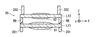
- FIG. 6 and 7 are schematic cross-sectional views of the lens group 20, and the direction indicated by the arrow AR2 corresponds to the + Z direction.
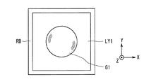
- 8 is a bottom view of the lens group 20 when the lens group 20 is viewed from below ( ⁇ Z side)
- FIG. 9 is a top view of the lens group 20 when the lens group 20 is viewed from above (+ Z side). It is.
- the lens group 20 includes a first lens constituent layer LY1 having a first lens G1, a second lens constituent layer LY2 having a second lens G2, and a spacer layer RB. . Then, the first lens constituent layer LY1 and the second lens constituent layer LY2 are coupled via the spacer layer RB.
- the outer edges of the non-lens portions of the first and second lens constituent layers LY1, LY2 have a substantially square shape.
- the first lens constituting layer LY1 having the first lens G1 has a first main surface (here, the ⁇ Z side) on the first non-lens portion that does not function as a lens.
- a protrusion 201 is provided.
- a non-lens portion that does not function as a lens is provided on one main surface (here, + Z side) of the second lens constituent layer LY ⁇ b> 2 having the second lens G ⁇ b> 2.
- a second protrusion 202 is provided.
- FIG. 10 is a view of the spacer layer RB as viewed from above (+ Z side) focusing on the shape of the spacer layer RB.
- the spacer layer RB is provided along the outer edge of the non-lens portion of the first and second lens constituting layers LY1 and LY2, and the outer edge and the inner edge of the XY cross section are rectangular in shape. It has a configuration. Then, the optical axis of the lens group 20 is set in a direction along the Z axis.
- each functional layer which comprises the camera module 500 is demonstrated.
- the ⁇ Z side surface is referred to as one main surface
- the + Z side surface is referred to as the other main surface.
- the image sensor layer 18 receives light from the subject that has passed through the optical unit KB, and generates an image signal related to the image of the subject, its peripheral circuit, and the image sensor 181. It is a member provided with the outer peripheral part which surrounds.
- the image sensor 181 is configured by arranging a large number of pixel circuits. Note that a solder ball HB for performing soldering by a reflow method is provided on one main surface (the surface on the ⁇ Z side) of the imaging element layer 18.
- various types of wiring for applying a signal to the image sensor 181 and reading a signal from the image sensor 181 are connected to one main surface of the image sensor layer 18. A terminal is provided.
- the cover glass layer 17 has a substantially flat plate shape and an XY cross section having a substantially square shape, and is made of transparent glass or the like.
- the cover glass layer 17 is bonded to the other main surface (+ Z side surface) of the image sensor layer 18 and has a function of protecting the image sensor 181.
- the image sensor substrate 178 is configured with the cover glass layer 17 bonded to the image sensor layer 18.
- the lens position adjustment layer 16 is configured by using a resin material, is disposed between the image sensor 181 and the lens group 20, and is a member that adjusts the distance between the image sensor 181 and the lens group 20. Specifically, the lens position adjustment layer 16 defines the position (initial position) of the lens group 20 in the non-driven state.
- the lens position adjustment layer 16 is generated using, for example, a method of etching a resin.
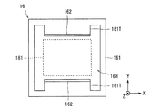
- FIG. 11 is a top view of the lens position adjusting layer 16 as seen from above (+ Z side).
- FIG. 12 is a side view of the lens position adjusting layer 16 when the lens position adjusting layer 16 is viewed from the side.
- the lens position adjustment layer 16 includes a frame body 161 and a protrusion 162.
- the frame body 161 is a substantially rectangular annular portion constituting the outer peripheral portion of the lens position adjusting layer 16, and has a plate-like shape substantially parallel to the XY plane.
- the frame body 161 forms a hole (through hole) 16H penetrating in the direction along the Z-axis.
- the + Y side plate-like member and the ⁇ Y side plate-like member constituting the frame body 161 are: Each has a protruding portion 161T that protrudes toward the through hole 16H.
- one main surface of the frame body 161 is bonded to the adjacent cover glass layer 17, and the other main surface of the frame body 161 is connected to the adjacent actuator layer 15 (specifically, the frame body 15 f of the actuator layer 15 ( FIG. 13)).
- the projecting portion 162 is erected upward (in the + Z direction) in the vicinity of the inner edge of the convex portion 161T constituting the frame body 161.
- the projection 162 is a plate-like portion having a substantially rectangular board surface substantially parallel to the XZ plane, and the longitudinal direction of the projection 162 is a direction substantially parallel to the X axis, and the short direction of the projection 162 Is a direction substantially parallel to the Z-axis.
- the end surface on the + Z side of the protrusion 162 has a function of placing the lens group 20 at the initial position when the lens group 20 comes into contact therewith.
- an area where a plurality of pixel circuits constituting the image sensor 181 are arranged is indicated by a broken line.
- the protrusion 162 is disposed at a position that sandwiches the optical path from the subject through the lens group 20 to the pixel array region of the image sensor 181 in the direction in which the width of the pixel array region is the narrowest. That is, the protrusion 162 is installed so as not to adversely affect the photographing and increase the size of the apparatus.
- FIG. 13 is a top view of the actuator layer 15 as seen from above (+ Z side).
- FIG. 14 is a side view of the actuator layer 15 as seen from the side.
- FIGS. 15 to 18 are diagrams showing the configuration of each layer constituting the actuator layer 15.
- the actuator layer 15 includes a frame body 15 f constituting an outer peripheral portion, and two plate-like movable portions that protrude from the frame body 15 f with respect to a hollow portion inside the frame body 15 f. 15a and 15b.
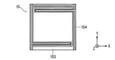
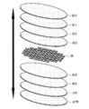
- the actuator layer 15 includes a base layer 151 (FIG. 15), an actuator element layer 152 (FIG. 16), an insulating layer 153 (FIG. 17), and a heater layer 154 (FIG. 18) from the ⁇ Z side to the + Z side. Laminated in this order.
- the base layer 151 includes a base frame body 151f constituting the frame body 15f, and two plate-like projecting portions 151a and 151b that project from the base frame body 151f with respect to a hollow portion inside the base frame body 151f. Is provided.
- the protruding portion 151a as the base portion constitutes the movable portion 15a
- the protruding portion 151b as the base portion constitutes the movable portion 15b.
- the base layer 151 is made of a material having a low coefficient of thermal expansion such as silicon.
- Actuator element layer 152 has force generating part 152a that constitutes movable part 15a, and force generating part 152b that constitutes movable part 15b.
- the force generators 152a and 152b are made of a material having characteristics different from those of the base layer 151, and generate force by being deformed in response to heating.
- the description will be made assuming that the force generation units 152a and 152b are made of a shape memory alloy (SMA).
- the force generation part 152a is formed so as to cover the entire area of the + Z side main surface (other main surface) of the protruding part 151a by a technique such as sputtering or vapor deposition.
- the force generation part 152b is formed so as to cover the entire area of the + Z side main surface (other main surface) of the projecting portion 151b by a technique such as sputtering.
- the insulating layer 153 is made of an insulator such as silica (silicon dioxide).
- the insulating layer 153 is formed so as to cover the entire area of the main surface (other main surface) on the + Z side of the base frame 151f and the actuator element layer 152 by a technique such as sputtering or vapor deposition.
- the heater layer 154 is made of a conductive metal such as platinum having a high resistivity.
- the heater layer 154 is formed on the main surface (other main surface) on the + Z side of the insulating layer 153 by a photolithography technique generally used in a semiconductor manufacturing process or the like.
- the wiring portion 1541, the heater portion 154b, the wiring portion 1542, the heater portion 154a, and the wiring portion 1543 are extended in this order, and are sequentially electrically connected.
- the wiring portions 1541, 1542, and 1543 constitute the frame 15f
- the heater portion 154a constitutes the movable portion 15a
- the heater portion 154b constitutes the movable portion 15b.
- the wiring portions 1541, 1542, and 1543 are configured to be wider and have lower electrical resistance than the heater portions 154a and 154b. Accordingly, when a voltage is applied between one end of the heater layer 154 (specifically, the end surface on the ⁇ Y side of the wiring portion 1541) and the other end (the end surface on the ⁇ Y side of the wiring portion 1543), the electrical resistance Heater parts 154a and 154b having a high temperature generate heat due to their own Joule heat. That is, the heater portions 154a and 154b as the heat generating portions generate heat in response to current supply.
- FIG. 19 is a top view showing a detailed configuration of the actuator layer 15 when the actuator layer 15 is viewed from above (+ Z side).
- the heater layer 154 is formed on the other main surface (+ Z side surface) of the actuator layer 15. Specifically, the heater portion 154a extends from one end portion (fixed end) fixed to the frame 15f of the movable portion 15a to the vicinity of the other end portion (free end) FT of the movable portion 15a. It is folded in the vicinity of the free end FT and extends from the vicinity of the free end FT to the fixed end.
- the heater portion 154b extends from one end portion (fixed end) fixed to the frame 15f of the movable portion 15b to the vicinity of the other end portion (free end) FT of the movable portion 15b. It is folded near the free end FT and extends from the free end FT to the fixed end. Further, one end (specifically, the ⁇ Y side end face of the wiring portion 1541) and the other end (the ⁇ Y side end face of the wiring portion 1543) of the heater layer 154 are exposed on the side surface of the camera module 500. A voltage and a current are supplied to one end and the other end of the heater layer 154 via the side wiring 21 (FIGS. 3 to 5).
- the actuator layer 15 is subjected to a process (shape memory process) in which the movable parts 15a and 15b are set in a mold having a shape to be memorized and heated at a predetermined temperature (for example, 600 ° C.).
- the SMA constituting the actuator element layer 152 has a characteristic of being restored to a predetermined shape (also referred to as “memory shape”) stored in advance when heated to exceed a predetermined phase transformation temperature and reach a predetermined temperature.
- a warped shape in which the free ends FT of the movable portions 15a and 15b are displaced upward (+ Z direction) is stored.
- FIGS. 20 and 21 are schematic views showing a mode in which the movable portions 15a and 15b are deformed in response to heat generated by the heater portions 154a and 154b.
- transformation aspect of movable part 15a, 15b is respectively the same, in FIG. 20 and FIG. 21, the deformation
- the movable portion 15 a has a flat shape in a state where the heater portion 154 a does not generate heat.
- a force is generated by the deformation of the force generator 152a in response to the heat generated by the heater 154a, and the movable portion 15a is fixed to the frame 15f. With the vicinity of the (fixed end) as a fulcrum, deformation occurs such that the free end FT is displaced upward (+ Z direction).
- FIG. 22 is an external view of the lower surface of the second parallel spring 14 when the second parallel spring 14 is viewed from below ( ⁇ Z direction).
- FIG. 23 is a view showing the second parallel spring 14 joined to the lens group 20.
- the second parallel spring 14 is an elastic member having a fixed frame body 141 and an elastic portion 142, and is a layer (elastic layer) forming a spring mechanism.
- SUS type metal material or phosphor bronze etc. are employ
- the fixed frame 141 constitutes the outer peripheral portion of the second parallel spring 14 and is joined to the frame 15f of the adjacent actuator layer 15.
- the distance between the heater layer 154 of the actuator layer 15 and the second second parallel spring 14 is usually only about 10 ⁇ m.
- the side wiring 21 for supplying voltage and current to the heater layer 154 is simply provided from the imaging element layer 18 to the actuator layer 15 by printing or the like, for example, the side wiring 21 extends to the fixed frame 141. End up. That is, the side wiring 21 and the second parallel spring 14 are short-circuited.
- a notch 143 that is recessed at the outer edge in the vicinity of the four corners of the fixed frame 141 of the second parallel spring 14 is provided.
- the notch 143 is an epoxy system used for joining when the second frame layer 13 and the second parallel spring 14 are joined and when the second parallel spring 14 and the actuator layer 15 are joined.
- Insulating portion 14ep (FIGS. 3 and 4) is formed by filling an adhesive such as resin. Due to the presence of the insulating portion 14ep, unnecessary short circuit due to contact between the side wiring 21 and the second parallel spring 14 is prevented.
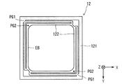
- the elastic part 142 has a connection part PG1 with the fixed frame body 141 and a joint part PG2 with the lens group 20, and the connection part PG1 and the joint part PG2 are connected by a plate-like member EB.
- the second parallel spring 14 is joined to the lens group 20 at a joint portion PG2 provided in the elastic portion 142.
- the first protrusion 201 contacts the free end FT of the actuator layer 15 through the gap between the fixed frame 141 of the second parallel spring 14 and the plate member EB. That is, the second parallel spring 14 has a shape that does not contact the first protrusion 201 of the lens group 20.
- the second parallel spring 14 can be elastically deformed in the optical axis direction ( ⁇ Z direction) of the lens group 20 by elastic deformation of the plate-like member EB, and functions as a spring mechanism.
- the second parallel spring 14 is manufactured using a SUS metal material or phosphor bronze.
- a resist in the shape of a parallel spring is patterned on the metal material by a photolithography technique, and dipped in an iron chloride-based etching solution to be wet. Etching is performed to form a parallel spring pattern.
- the second frame layer 13 is a ring-shaped member in which the outer edge and the inner edge of the XY cross section are each substantially rectangular, and forms a hollow portion that penetrates along the Z-axis.
- the second frame layer 13 surrounds the lens group 20 from the side by arranging the lens group 20 in the hollow portion.
- resin, glass, etc. are mentioned as a raw material which comprises the 2nd frame layer 13,
- the 2nd frame layer 13 is manufactured by what is called a press method using a metal metal mold
- the lower end surface (one main surface) located on the ⁇ Z side of the second frame layer 13 is joined to the fixed frame body 141 of the adjacent second parallel spring 14. Further, the upper end surface (other main surface) located on the + Z side of the second frame layer is joined to the adjacent first parallel spring 12 (specifically, the fixed frame body 121 (FIG. 24) of the first parallel spring 12). Is done.
- FIG. 24 is an external view of the lower surface of the first parallel spring 12 when the first parallel spring 12 is viewed from below ( ⁇ Z direction).
- the first parallel spring 12 is an elastic member having the same configuration and function as the second parallel spring 14 except that the notch portion 143 is not provided. 121 and an elastic part 122.
- One main surface of the fixed frame 121 is joined to the other main surface of the adjacent second frame layer 13, and the other main surface of the fixed frame 121 is connected to the adjacent first frame layer 11 (in detail, the first 1 frame layer 11 at the ⁇ Z side lower end surface).
- FIG. 25 is a view showing the first parallel spring 12 joined to the lens group 20.
- the joint portion PG ⁇ b> 2 provided in the elastic portion 122 is joined to the upper end surface on the + Z side of the protrusion 202 of the lens group 20. For this reason, when the lens group 20 is moved relative to the fixed frame 121 in the + Z direction, elastic deformation occurs in the plate-like member EB, and the first parallel spring 12 functions as a spring mechanism.
- the first frame layer 11 is a ring-shaped member in which the outer edge and the inner edge of the XY cross section are each substantially rectangular like the second frame layer 13 and penetrates along the Z axis. Forming a hollow portion.
- the hollow portion of the first frame layer 11 becomes a space in which the plate-like member EB and the protruding portion 202 that are elastically deformed when the lens group 20 is moved in the + Z direction can move.
- the first frame layer 11 is formed by the same material and manufacturing method as the second frame layer 13.
- the lower end surface (one main surface) located on the ⁇ Z side of the first frame layer 11 is joined to the fixed frame body 121 of the adjacent first parallel spring 12.
- the upper end surface (other end surface) located on the + Z side of the first frame layer is joined to the adjacent lid layer 10 (specifically, near the outer peripheral portion of the lid layer).
- the outer edge of the XY cross section has a substantially square shape
- the lid layer 10 has a hole (through hole) 10 ⁇ / b> H penetrating in a direction parallel to the Z axis at a substantially center, and is substantially in the XY plane. It is a plate-like member having a parallel board surface.
- the through hole 10H is a hole for guiding light from the subject to the image sensor 181 through the lens group 20, and the lid layer 10 is formed by pressing a flat resin material or patterning the resin material.
- the through hole 10H is formed and manufactured by a method of etching later.
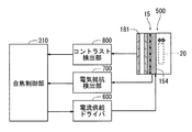
- FIG. 26 is a block diagram illustrating a functional configuration related to autofocus control of the camera module 500.
- the electrical resistance detector 700 detects the electrical resistance of the heater layer 154 and outputs a signal indicating the electrical resistance to the focus control unit 310.
- the focusing control unit 310 detects the deformation of the movable units 15a and 15b (specifically, the displacement of the free end FT) based on the electric resistance of the heater layer 154.
- the detection of the displacement of the free end FT is performed by utilizing the fact that the relationship between the shape and electric resistance in the heater layer 154 (specifically, the heater portions 154a and 154b) is uniquely determined.
- the focus control unit 310 controls the current supplied to the heater layer 154 via the current supply driver 600 while detecting the displacement of the free end FT, so that the deformation amount of the movable units 15a and 15b, that is, free Control the displacement of the end FT.
- the lens group 20 is moved in the + Z direction, so that the separation distance between the lens group 20 and the image sensor 181 is changed, and the focal point of the optical unit KB. The position of is changed.
- the contrast detection unit 800 detects the contrast of the image signal obtained by the image sensor 181. For example, a numerical value obtained by accumulating differences in gradation values between adjacent pixels for the entire image is detected as an evaluation value indicating contrast. A signal indicating the evaluation value indicating the contrast is output to the focus control unit 310.
- the separation distance between the lens group 20 and the image sensor 181 is sequentially set to a preset multi-step separation distance under the control of the focusing control unit 310, and each separation distance is set.
- an image signal is acquired by the image sensor 181.
- the extension position of the lens group 20 in the + Z direction is set to a preset multistage position, and an image signal is output by the image sensor 181 at the time when the lens group 20 is disposed at each extension position.
- the focus control unit 310 controls the supply of current to the heater layer 154 via the current supply driver 600 while monitoring the electrical resistance of the heater layer 154 detected by the electrical resistance detection unit 700.
- the extended position of the lens group 20 is changed.
- the focus control unit 310 detects a feeding position where the evaluation value indicating the contrast is maximum based on the evaluation value indicating the contrast detected for each feeding position by the contrast detection unit 800.
- the state where the lens group 20 is disposed at the extended position where the evaluation value indicating the contrast is maximum corresponds to the state where the subject is in focus.
- the lens group 20 is moved to the extended position where the evaluation value indicating the contrast is maximized, thereby achieving focusing on the subject in the camera module 500. That is, autofocus control is realized.
- the heater portion 154a is provided in a region located in a direction opposite to the direction in which the protruding portion 151a exists with respect to the force generating portion 152a, and in the movable portion 15b.
- the heater portion 154b is provided in a region located in a direction opposite to the direction in which the protruding portion 151b exists with reference to the force generating portion 152b.
- the heater portions 154a and 154b are spaced apart from the vicinity (neutral surface) of the projecting portions 151a and 151b due to the presence of the force generating portions 152a and 152b and the insulating layer 153. For this reason, when the free ends FT of the movable parts 15a and 15b are displaced upward, relatively large deformations occur in the heater parts 154a and 154b. As a result, a greater change in electrical resistance in the heater layer 154 is obtained with respect to the displacement of the free ends FT of the movable portions 15a and 15b.
- the deformation in the heaters 154a and 154b and the amount of change in electrical resistance are sufficiently generated with respect to the deformation of the movable parts 15a and 15b. Therefore, the deformation amount of each movable part 15a, 15b can be controlled with high accuracy.
- FIG. 27 is a flowchart showing the manufacturing process of the camera module 500.
- process A generation of the lens group 20 (step SP1)
- step SP2 sheet preparation
- step SP3 assembly jig preparation
- step SP3 assembly jig preparation
- step SP4 First bonding of the sheet
- step SP5 Mounting of the lens group 20
- Step SP6 Second bonding of the sheet
- Step SP6 Second bonding of the sheet
- Step SP8 Second bonding of the sheet
- Step SP7 Image sensor substrate 178
- process H dicing
- step SP1 the lens group 20 is generated.
- a wafer in which a large number of lens groups 20 are arranged in a matrix (hereinafter also referred to as a “lens group wafer”) is manufactured, and a large number of lens groups 20 are separated into pieces by dicing. Group 20 is produced.
- the lens group wafer includes a wafer in which a large number of first lens constituent layers LY1 are arranged (first lens constituent layer wafer), a wafer in which a large number of spacer layers RB are arranged (spacer layer wafer), and a large number of second lenses.
- a wafer (second lens constituent layer wafer) on which the constituent layers LY2 are arranged is laminated and bonded together.
- step SP2 a sheet relating to each functional layer constituting the camera module 500 is formed for each layer.
- a disc-shaped sheet at the wafer level is prepared.
- a large number of chips corresponding to members related to the functional layer are formed in a matrix on the sheet for each functional layer.
- the functions such as the lid layer 10, the first frame layer 11, the first parallel spring 12, the second frame layer 13, the second parallel spring 14, the actuator layer 15, and the lens position adjustment layer 16 are performed.
- Each sheet U10 to U16 on which a large number of chips related to the layers are formed in a predetermined arrangement, and a sheet (image pickup element) including chips related to the image pickup element substrate 178 formed by bonding the cover glass layer 17 and the image pickup element layer 18 Substrate sheet) U178 is prepared. That is, eight sheets U10 to 16 and U178 are prepared.
- an assembly jig is prepared.
- the assembling jig is configured by providing a plurality of protrusions having substantially the same shape on a flat base in a predetermined arrangement.
- alignment marks for alignment are formed at two or more predetermined locations.
- the upper surface of the protrusion is configured to be substantially parallel to the main surface of the flat base.
- a unit corresponding to each camera module 500 is manufactured on the upper surface.
- step SP4 Three sheets U11 to U13 among the eight prepared sheets U10 to U16 and U178 are joined.
- the first frame layer sheet U11, the first parallel spring sheet U12, and the second frame layer sheet U13 are aligned in the sheet shape so that the chips included in the sheets U11 to U13 are stacked on each other. (Alignment) is performed. Then, the sheets U11 to U13 are joined using an adhesive or the like.
- FIG. 28 shows a state in which three sheets U11 to U13 are laminated and joined in step S4, a lens group 20 is attached in step S5, and four sheets U10 and U14 to U16 are laminated in step S6. It is a figure which shows typically a mode that it joins and a mode that the image pick-up element board
- step SP5 the lens group 20 generated in step SP1 is attached to a hollow portion of each second frame layer 13 of the unit manufactured in step SP4 by a predetermined mounter. That is, the lens group 20 is inserted into each gap of the second frame layer sheet U13 having a lattice shape. Specifically, while the lens group 20 is pressed against the joint PG2, the end surface of the second protrusion 202 is joined to the one main surface side of the joint PG2.
- this joining method etc. which join using the adhesive agent (UV curing adhesive) hardened
- step SP6 Sheet second joining (process F)>
- step SP6 four sheets U10, U14 to U16 of the eight sheets U10 to U16 and U178 prepared in step SP2 are joined.
- each chip included in the second parallel spring sheet U14 and the actuator layer sheet U15 is attached to the second frame layer sheet with respect to one main surface side of the units generated up to step SP5.
- Positioning (alignment) is performed while maintaining the sheet shape so as to be stacked on each chip included in U13.
- seat U14, U15 is joined using an adhesive agent etc. in order.
- the sheet is so formed that each chip included in the lid layer sheet U10 is stacked with respect to each chip included in the first frame layer sheet U11 with respect to the other main surface side of the first frame layer sheet U11. Alignment (alignment) is performed in the shape. In this state, the lid layer sheet U10 is bonded to the other main surface side of the first frame layer sheet U11 using an adhesive or the like.
- the sheet-like shape is formed so that each chip included in the lens position adjustment layer sheet U16 is stacked on each chip included in the actuator layer sheet U15 with respect to one main surface side of the actuator layer sheet U15.
- the alignment is performed as it is.
- the lens position adjustment layer sheet U16 is bonded to one main surface side of the actuator layer sheet U15 using an adhesive or the like.
- step SP7 the lens is arranged so that the outer peripheral portion of the image sensor substrate 178 is bonded to the frame 161 of the lens position adjustment layer 16 of the unit formed by bonding the lens position adjustment layer 16 by step SP6.
- the other main surface of the imaging element substrate sheet U178 is joined to one main surface of the position adjustment layer sheet U16.
- step SP8 a large number of lens groups 20 are respectively inserted, and a laminated member formed by laminating eight sheets U10 to U16 and U178 is protected by a dicing tape or the like and then separated for each chip by a dicing device. .
- a large number of camera modules 500 are completed.
- the side wiring 21 is formed. Specifically, when dicing along one direction is performed, each heater layer 154 is exposed at a cut surface corresponding to the side surface of each camera module 500. Therefore, a conductive material for forming the side wiring 21 is applied to the cut surface, and then dicing along the other direction is performed, so that a large number of camera modules 500 are completed.
- the actuator layer 15 includes the force generators 152a and 152b that generate force in response to heating, Heater portions 154a and 154b, which are portions that generate heat in response to supply, are provided separately.
- the displacement of the free ends FT in the movable portions 15a and 15b is controlled by supplying a current to the heater portions 154a and 154b in accordance with the electric resistance in the heater portions 154a and 154b. Therefore, it is possible to control the displacement of the movable parts 15a and 15b, and to design the force generating parts 152a and 152b and the heater parts 154a and 154b separately. Therefore, the actuator layer 15 having a configuration capable of controlling the displacement in the movable portions 15a and 15b and having a high degree of design freedom is realized.
- the force generation parts 152a and 152b are made of a shape memory alloy, the deformation of the movable parts 15a and 15b greatly occurs when current is applied. Therefore, the movable parts 15a and 15b can be efficiently deformed.
- the heater portion 154a is provided in a region located in a direction opposite to the direction in which the projecting portion 151a exists with respect to the force generating portion 152a.
- the heater part 154b is provided in the area
- the heater portion 154a may be provided in a region between the protruding portion 151a and the force generating portion 152a, or the heater portion 154b is provided in a region between the protruding portion 151b and the force generating portion 152b. May be.
- the heater portion 154a is from the vicinity of the lower surface of the projecting portion 151a, the larger the deformation amount of the heater portion 154a when the movable portion 15a is deformed, and the heater portion 154b is moved from the vicinity of the lower surface of the projecting portion 151b.
- the further away the greater the amount of deformation of the heater part 154b when the movable part 15b is deformed.
- the heater part 154a is separated as much as possible from the vicinity of the lower surface of the projecting part 151a as in the above embodiment, and the heater It is preferable that the portion 154b is separated as much as possible from the vicinity of the lower surface of the protruding portion 151b. Therefore, it is preferable that the heater portion 154a is not provided on the lower surface of the protruding portion 151a and the heater portion 154b is not provided on the lower surface of the protruding portion 151b.
- the force generators 152a and 152b are made of a shape memory alloy, but the present invention is not limited to this.
- the force generators 152a and 152b may be made of a material having a thermal expansion coefficient higher than that of the material forming the base layer 151 instead of the shape memory alloy.
- the base layer 151 is formed of a material having a relatively small thermal expansion coefficient such as silicon
- the force generating portions 152a and 152b are formed of a material having a relatively large thermal expansion coefficient such as aluminum or nickel. (Bi-metallic strip) may be applied.
- the force generators 152a and 152b can be formed using a material that is less expensive than when a shape memory alloy is used. For this reason, the manufacturing cost of the actuator layer 15 can be reduced.
- each of the movable portions 15a and 15b is configured by overlapping the protruding portions 151a and 151b, the force generating portions 152a and 152b, the insulating layer 153, and the heater portions 154a and 154b. It is not limited to this.
- each movable part 15a, 15b is provided with a protruding part 151a, 151b, a force generating part 152a, 152b, and the like, such as disposing an insulating layer between the protruding parts 151a, 151b and the force generating parts 152a, 152b.
- the projecting portions 151a and 151b, the force generating portions 152a and 152b, and the heater portions 154a and 154b each have a layered shape.
- the present invention is not limited to this.
- a structure having a certain thickness is adopted for the heater parts 154a, 154b, and a plurality of parts including the projecting parts 151a, 151b, the force generating parts 152a, 152b, and the heater parts 154a, 154b are employed.
- a structure in which portions are overlapped may be employed.
- the plate-like first and second parallel springs 12 and 14 are employed as members for restricting the movement of the lens group 20, but the present invention is not limited to this.
- various elastic members including a helical spring may be employed.
- the object moved by the movable parts 15a and 15b is the lens group 20 as an optical system, but is not limited thereto.
- other members such as an image sensor may be used as the moving object.
- the lens group 20B corresponding to the optical system that guides light from the subject to the image sensor is fixed, and the image sensor layer is moved in the Z direction by a configuration similar to the configuration for moving the lens group 20 in the one embodiment. Also good.
- FIG. 29 is a diagram illustrating a conceptual diagram of one aspect in which the lens group 20B is fixed and the imaging element layer 18B is moved back and forth in a direction along the optical axis Ax of the lens group 20B.
- an imaging unit PBB that moves the imaging element layer 18B back and forth along the optical axis Ax is depicted.
- the image pickup element layer 18B is moved back and forth along the optical axis Ax according to the operation of the actuator layer, and the distance between the lens group 20B and the image pickup element layer 18B is changed. Control is realized.
- the imaging device using the actuator layer 15 which can control the displacement in the movable parts 15a and 15b and has a high degree of design freedom is realized.
- an object (moving object) moved by the actuator is not limited to an element constituting the imaging apparatus such as an optical system or an imaging element.
- the moving object may be another object such as an objective lens of an optical pickup lens. That is, the present invention can be applied to an actuator and a drive device in which a moving object is moved according to bending deformation of the actuator.
Landscapes
- Engineering & Computer Science (AREA)
- Chemical & Material Sciences (AREA)
- Combustion & Propulsion (AREA)
- Mechanical Engineering (AREA)
- General Engineering & Computer Science (AREA)
- Physics & Mathematics (AREA)
- General Physics & Mathematics (AREA)
- Optics & Photonics (AREA)
- Lens Barrels (AREA)
- Studio Devices (AREA)
Abstract
Description
図1は、本発明の一実施形態に係るカメラモジュール500を搭載した携帯電話機100の概略構成を示す模式図である。なお、図1および図1以降の図では方位関係を明確化するために、XYZの相互に直交する3軸が適宜付されている。
図3は、カメラモジュール500の断面模式図であり、図3の矢印AR1の示す方向が+Z方向に対応する。なお、図3以降の図面においても、方位関係の明確化のために、+Z方向に対応する方向を示す矢印AR1が適宜付されている。また、図4および図5は、カメラモジュール500を側方から見た側面図である。
レンズ群20は、ガラス基板を基材としてウエハレベルで作製され、例えば、2枚以上のレンズを重ね合わせて成形される。本実施形態では、2枚の光学レンズを重ね合わせてレンズ群20が構成される場合について例示する。なお、本実施形態では、レンズ群20は、被写体からの光を撮像素子181に導く撮像レンズとして機能する。
以下では、カメラモジュール500を構成する各機能層の詳細について説明する。なお、各機能層については、-Z側の面を一主面と称し、+Z側の面を他主面と称する。
図3で示されるように、撮像素子層18は、光学ユニットKBを通過した被写体からの光を受光して、被写体の像に関する画像信号を生成する撮像素子181、その周辺回路、および撮像素子181を囲む外周部を備える部材である。また、撮像素子181は、多数の画素回路が配列されて構成される。なお、撮像素子層18の一主面(-Z側の面)には、リフロー方式によるはんだ付けを行うためのはんだボールHBが設けられている。また、ここでは図示を省略しているが、撮像素子層18の一主面には、撮像素子181に対する信号の付与、および該撮像素子181からの信号の読み出しを行う配線を接続するための各種端子が設けられる。
図3で示されるように、カバーガラス層17は、略平板状であり且つXY断面が略正方形の形状を有し、透明なガラス等によって構成される。このカバーガラス層17は、撮像素子層18の他主面(+Z側の面)に対して接合され、撮像素子181を保護する機能を有する。なお、カバーガラス層17が撮像素子層18上に接合された状態で撮像素子基板178を構成する。
レンズ位置調整層16は、樹脂材料を用いて構成されるとともに、撮像素子181とレンズ群20との間に配設され、且つ撮像素子181とレンズ群20との距離を調整する部材である。具体的には、レンズ位置調整層16は、非駆動状態におけるレンズ群20の位置(初期位置)を規定する。なお、レンズ位置調整層16は、例えば、樹脂をエッチングする手法等を用いて生成される。
図13は、アクチュエータ層15を上方(+Z側)から見た該アクチュエータ層15の上面図である。図14は、アクチュエータ層15を側方から見た該アクチュエータ層15の側面図である。図15から図18は、アクチュエータ層15を構成する各層の構成を示す図である。
図22は、第2平行ばね14を下方(-Z方向)から見た該第2平行ばね14の下面外観図である。図23は、レンズ群20に接合された第2平行ばね14を示す図である。図22で示されるように、第2平行ばね14は、固定枠体141と、弾性部142とを有する弾性部材であり、ばね機構を形成する層(弾性層)となっている。なお、第2平行ばね14の素材としては、例えば、SUS系の金属材料またはりん青銅等が採用される。
図3で示されるように、第2枠層13は、XY断面の外縁および内縁がそれぞれ略矩形状であるリング状の部材であり、Z軸に沿って貫通する中空部分を形成する。第2枠層13は、中空部分にレンズ群20が配置されることで、該レンズ群20を側方から囲む。なお、第2枠層13を構成する素材としては、樹脂やガラス等が挙げられ、第2枠層13は、金属金型を用いたいわゆるプレス法や射出成型法等によって製作される。そして、第2枠層13の-Z側に位置する下端面(一主面)は、隣接する第2平行ばね14の固定枠体141と接合される。また、第2枠層の+Z側に位置する上端面(他主面)は、隣接する第1平行ばね12(詳細には、第1平行ばね12の固定枠体121(図24))と接合される。
図24は、第1平行ばね12を下方(-Z方向)から見た該第1平行ばね12の下面外観図である。図24で示されるように、第1平行ばね12は、切り欠き部143が設けられていないことを除いて、第2平行ばね14と同様の構成および機能を有する弾性部材であり、固定枠体121と弾性部122とを備える。そして、固定枠体121の一主面は、隣接する第2枠層13の他主面と接合され、固定枠体121の他主面は、隣接する第1枠層11(詳細には、第1枠層11の-Z側の下端面)と接合される。
図3で示されるように、第1枠層11は、第2枠層13と同様に、XY断面の外縁および内縁がそれぞれ略矩形状であるリング状の部材であり、Z軸に沿って貫通する中空部分を形成する。第1枠層11の中空部分は、レンズ群20が+Z方向に移動される際に、弾性変形する板状部材EBおよび突起部202が移動可能な空間となる。なお、第1枠層11は、第2枠層13と同様な素材および製作方法によって形成される。そして、第1枠層11の-Z側に位置する下端面(一主面)は、隣接する第1平行ばね12の固定枠体121と接合される。また、第1枠層の+Z側に位置する上端面(他端面)は、隣接する蓋層10(詳細には、蓋層の外周部近傍)と接合される。
図3で示されるように、蓋層10は、XY断面の外縁が略正方形であるとともに、略中央にZ軸に平行な方向に貫通する孔(貫通孔)10Hを有し、XY平面に略平行な盤面を有する板状の部材である。貫通孔10Hは、被写体からの光をレンズ群20を介して撮像素子181に導くための孔であり、この蓋層10は、平板状の樹脂材料をプレス加工する手法、あるいは樹脂材料をパターニングした後にエッチングする手法によって、貫通孔10Hが形成されて製作される。
図26は、カメラモジュール500のオートフォーカス制御に係る機能的な構成を示すブロック図である。電気抵抗検出部700は、ヒータ層154の電気抵抗を検出し、該電気抵抗を示す信号を合焦制御部310に対して出力する。合焦制御部310は、ヒータ層154の電気抵抗に基づいて、可動部15a,15bの変形(具体的には、自由端FTの変位)を検出する。この自由端FTの変位の検出については、ヒータ層154(具体的には、ヒータ部154a,154b)における形状と電気抵抗との関係が一義的に決まることが利用されて実行される。そして、合焦制御部310は、自由端FTの変位を検出しつつ、電流供給ドライバ600を介してヒータ層154に供給する電流を制御することで、可動部15a,15bの変形量、すなわち自由端FTの変位を制御する。このとき、自由端FTによる第1突起部201の押し上げにより、レンズ群20が+Z方向に移動されることで、レンズ群20と撮像素子181との離隔距離が変更されて、光学ユニットKBの焦点の位置が変更される。
ここで、カメラモジュール500の製造工程について簡単に説明する。図27は、カメラモジュール500の製造工程を示すフローチャートである。図27で示されるように、(工程A)レンズ群20の生成(ステップSP1)、(工程B)シートの準備(ステップSP2)、(工程C)組み立て治具の準備(ステップSP3)、(工程D)シートの第1の接合(ステップSP4)、(工程E)レンズ群20の取り付け(ステップSP5)、(工程F)シートの第2の接合(ステップSP6)、(工程G)撮像素子基板178の取り付け(ステップSP7)、および(工程H)ダイシング(ステップSP8)が順次に行われて、カメラモジュール500が製造される。
ステップSP1では、レンズ群20が生成される。ここでは、まず、多数のレンズ群20がマトリックス状に配列されたウエハ(以下「レンズ群ウエハ」とも称する)が製作され、ダイシングにより、多数のレンズ群20が個片化されて、多数のレンズ群20が製作される。レンズ群ウエハは、多数の第1レンズ構成層LY1が配列されたウエハ(第1レンズ構成層ウエハ)と、多数のスペーサ層RBが配列されたウエハ(スペーサ層ウエハ)と、多数の第2レンズ構成層LY2が配列されたウエハ(第2レンズ構成層ウエハ)とが積層されて、相互に接合されることで製作される。
ステップSP2では、カメラモジュール500を構成する各機能層に係るシートが、層ごとに形成される。なお、ここでは、ウエハレベルの円盤状のシートが準備される。機能層ごとのシートには、該機能層に係る部材に相当するチップがマトリクス状に所定配列で多数形成される。具体的には、ステップSP2では、蓋層10、第1枠層11、第1平行ばね12、第2枠層13、第2平行ばね14、アクチュエータ層15、およびレンズ位置調整層16といった各機能層に係るチップがそれぞれ所定配列で多数形成された各シートU10~U16、ならびにカバーガラス層17と撮像素子層18とが接合されて形成される撮像素子基板178に係るチップを含むシート(撮像素子基板シート)U178がそれぞれ準備される。つまり、8枚のシートU10~16,U178が準備される。
ステップSP3では、組み立て治具が準備される。この組み立て治具は、平板状の基台上に略同一の形状を有する多数の突起部が所定配列で設けられて構成される。なお、組み立て治具には、2カ所以上の所定の箇所に位置合わせのためのアライメントマークが形成される。また、突起部の上面は、平板状の基台の主面に対して略平行となるように構成される。なお、該上面上で各カメラモジュール500に相当するユニットが製作される。
ステップSP4では、準備された8枚のシートU10~16,U178のうちの3枚のシートU11~U13が接合される。ここでは、第1枠層シートU11、第1平行ばねシートU12、および第2枠層シートU13について、各シートU11~U13に含まれる各チップが互いに積層されるように、シート形状のまま位置合わせ(アライメント)が行われる。そして、各シートU11~U13が接着剤等を用いて接合される。
ステップSP5では、ステップSP4で製作されたユニットの各第2枠層13の中空部分に、ステップSP1で生成されたレンズ群20が、所定のマウンターによって取り付けられる。つまり、格子状の形状を有する第2枠層シートU13の各空隙に、レンズ群20がそれぞれ挿入される。具体的には、レンズ群20が接合部PG2に対して押し付けられつつ、第2突起部202の端面が、接合部PG2の一主面側に対して接合される。なお、この接合手法としては、紫外線の照射によって硬化する接着剤(紫外線硬化接着剤)を用いて接合する手法等が挙げられる。
ステップSP6では、ステップSP2で準備された8枚のシートU10~16,U178のうちの4枚のシートU10,U14~U16が接合される。具体的には、ステップSP6では、ステップSP5までに生成されたユニットの一主面側に対して、第2平行ばねシートU14、およびアクチュエータ層シートU15に含まれる各チップが、第2枠層シートU13に含まれる各チップに対してそれぞれ積層されるように、シート形状のまま位置合わせ(アライメント)が行われる。そして、各シートU14,U15が順次に接着剤等を用いて接合される。
ステップSP7では、ステップSP6までにレンズ位置調整層16が接合されて形成されたユニットのレンズ位置調整層16の枠体161に対して、撮像素子基板178の外周部が接合されるように、レンズ位置調整層シートU16の一主面に対して、撮像素子基板シートU178の他主面が接合される。
ステップSP8では、多数のレンズ群20がそれぞれ挿入され、8つのシートU10~U16,U178が積層されて形成された積層部材が、ダイシングテープ等で保護された後、ダイシング装置によってチップ毎に切り離される。このとき、多数のカメラモジュール500が完成される。なお、このダイシング工程の途中で、側面配線21が形成される。具体的には、一方向に沿ったダイシングが行われた時点で、各カメラモジュール500の側面に相当する切断面において、各ヒータ層154が露出する。このため、切断面に側面配線21を形成するための導電材料が塗布され、その後、他方向に沿ったダイシングが行われることで、多数のカメラモジュール500が完成される。
なお、本発明は上述の実施の形態に限定されるものではなく、本発明の要旨を逸脱しない範囲において種々の変更、改良等が可能である。
15a,15b 可動部
18,18B 撮像素子層
20,20B レンズ群
100 携帯電話機
151 ベース層
151a,151b 突設部
152 アクチュエータ素子層
152a,152b 力発生部
154 ヒータ層
154a,154b ヒータ部
181 撮像素子
310 合焦制御部
500 カメラモジュール
600 電流供給ドライバ
700 電気抵抗検出部
800 コントラスト検出部
Claims (6)
- 発熱に応じて変形する可動部と、
前記可動部の変形量を制御する制御部と、
を備え、
前記可動部が、
ベース部と、加熱に応じて力を発生する力発生部と、電流の供給に応じて発熱する発熱部とを含む複数の部分が重ねられている構造を有しており、
前記制御部が、
前記発熱部の電気抵抗に基づいて、前記発熱部に供給する電流を制御することで、前記可動部の変形量を制御することを特徴とするアクチュエータ。 - 請求項1に記載のアクチュエータであって、
前記発熱部が、
前記ベース部と前記力発生部との間の第1領域、および前記力発生部を基準として前記ベース部が存在する方向とは反対方向に位置する第2領域のうちの少なくとも一方の領域に設けられることを特徴とするアクチュエータ。 - 請求項1に記載のアクチュエータであって、
前記力発生部が、
形状記憶合金を含むことを特徴とするアクチュエータ。 - 請求項1に記載のアクチュエータであって、
前記力発生部が、前記ベース部の熱膨張率よりも高い熱膨張率を有することを特徴とするアクチュエータ。 - 請求項1に記載のアクチュエータと、
前記可動部の変形によって移動される移動対象物と、
を備えることを特徴とする駆動装置。 - 請求項1に記載のアクチュエータと、
撮像素子と、
被写体からの光を前記撮像素子まで導く光学系と、
を備え、
前記撮像素子および前記光学系のうちの少なくとも一方が、前記可動部の変形によって移動されることを特徴とする撮像装置。
Priority Applications (2)
| Application Number | Priority Date | Filing Date | Title |
|---|---|---|---|
| US13/260,557 US8421908B2 (en) | 2009-03-25 | 2010-03-16 | Actuator, drive device, and imaging device |
| JP2011505986A JP5348241B2 (ja) | 2009-03-25 | 2010-03-16 | アクチュエータ、駆動装置、および撮像装置 |
Applications Claiming Priority (2)
| Application Number | Priority Date | Filing Date | Title |
|---|---|---|---|
| JP2009074102 | 2009-03-25 | ||
| JP2009-074102 | 2009-03-25 |
Publications (1)
| Publication Number | Publication Date |
|---|---|
| WO2010110122A1 true WO2010110122A1 (ja) | 2010-09-30 |
Family
ID=42780814
Family Applications (1)
| Application Number | Title | Priority Date | Filing Date |
|---|---|---|---|
| PCT/JP2010/054434 Ceased WO2010110122A1 (ja) | 2009-03-25 | 2010-03-16 | アクチュエータ、駆動装置、および撮像装置 |
Country Status (3)
| Country | Link |
|---|---|
| US (1) | US8421908B2 (ja) |
| JP (1) | JP5348241B2 (ja) |
| WO (1) | WO2010110122A1 (ja) |
Cited By (2)
| Publication number | Priority date | Publication date | Assignee | Title |
|---|---|---|---|---|
| CN104564624A (zh) * | 2013-10-25 | 2015-04-29 | 埃贝斯佩歇气候控制系统有限责任两合公司 | 特别是用于为车辆加热器输送液体燃料的泵 |
| JP2024507527A (ja) * | 2021-02-22 | 2024-02-20 | ハッチンソン テクノロジー インコーポレイテッド | 形状記憶合金アクチュエータ及びその方法 |
Families Citing this family (18)
| Publication number | Priority date | Publication date | Assignee | Title |
|---|---|---|---|---|
| DE102013209819B4 (de) * | 2013-05-27 | 2018-01-25 | Fraunhofer-Gesellschaft zur Förderung der angewandten Forschung e.V. | Optische Struktur mit daran angeordneten Stegen und Verfahren zur Herstellung derselben |
| US9366879B1 (en) | 2014-12-02 | 2016-06-14 | Hutchinson Technology Incorporated | Camera lens suspension with polymer bearings |
| US9454016B1 (en) | 2015-03-06 | 2016-09-27 | Hutchinson Technology Incorporated | Camera lens suspension with integrated electrical leads |
| US10386131B2 (en) * | 2015-11-13 | 2019-08-20 | The Boeing Company | Self-regulating thermal insulation and related methods |
| US10670878B2 (en) | 2016-05-19 | 2020-06-02 | Hutchinson Technology Incorporated | Camera lens suspensions |
| KR20190015528A (ko) | 2016-06-09 | 2019-02-13 | 허친슨 테크놀로지 인코포레이티드 | 현가 조립체를 위한 접착제를 갖는 형상기억합금 와이어 부착 구조물 |
| US11448853B2 (en) | 2017-05-05 | 2022-09-20 | Hutchinson Technology Incorporated | Shape memory alloy actuators and methods thereof |
| US11333134B2 (en) | 2017-05-05 | 2022-05-17 | Hutchinson Technology Incorporated | Shape memory alloy actuators and methods thereof |
| US11815794B2 (en) | 2017-05-05 | 2023-11-14 | Hutchinson Technology Incorporated | Shape memory alloy actuators and methods thereof |
| US11306706B2 (en) | 2017-05-05 | 2022-04-19 | Hutchinson Technology Incorporated | Shape memory alloy actuators and methods thereof |
| US11105319B2 (en) | 2017-05-05 | 2021-08-31 | Hutchinson Technology Incorporated | Shape memory alloy actuators and methods thereof |
| GB2602950B (en) * | 2017-05-05 | 2022-10-26 | Hutchinson Technology | Shape memory alloy actuators and methods thereof |
| CN106950678A (zh) * | 2017-05-08 | 2017-07-14 | 广州市松诺电子有限公司 | 一种新型手机自动对焦马达 |
| CN209375770U (zh) * | 2018-01-25 | 2019-09-10 | 台湾东电化股份有限公司 | 光学系统 |
| CN115997156A (zh) * | 2020-06-09 | 2023-04-21 | 哈钦森技术股份有限公司 | 形状记忆合金致动器及其方法 |
| US11859598B2 (en) | 2021-06-10 | 2024-01-02 | Hutchinson Technology Incorporated | Shape memory alloy actuators and methods thereof |
| US12510061B2 (en) | 2023-04-12 | 2025-12-30 | Hutchinson Technology Incorporated | Shape memory alloy (SMA) bimorph actuators and methods for manufacturing the same |
| US11982263B1 (en) | 2023-05-02 | 2024-05-14 | Hutchinson Technology Incorporated | Shape metal alloy (SMA) bimorph actuators with reduced wire exit angle |
Citations (2)
| Publication number | Priority date | Publication date | Assignee | Title |
|---|---|---|---|---|
| JPS60195386A (ja) * | 1984-03-16 | 1985-10-03 | Nec Corp | 形状記憶アクチユエ−タ |
| JP2009013891A (ja) * | 2007-07-05 | 2009-01-22 | Konica Minolta Opto Inc | 形状記憶合金の駆動装置およびそれを用いる撮像装置 |
Family Cites Families (6)
| Publication number | Priority date | Publication date | Assignee | Title |
|---|---|---|---|---|
| JPS60219476A (ja) * | 1984-04-13 | 1985-11-02 | Toshiba Corp | アクチユエ−タ |
| JP2001142105A (ja) * | 1999-11-16 | 2001-05-25 | Minolta Co Ltd | 形状記憶合金を使用したアクチエータ |
| JP4191942B2 (ja) * | 2002-03-25 | 2008-12-03 | 株式会社アドバンテスト | スイッチ及びアクチュエータ |
| US7295770B2 (en) * | 2004-04-20 | 2007-11-13 | Pentax Corporation | Anti-shake apparatus |
| JP4736879B2 (ja) * | 2006-03-17 | 2011-07-27 | コニカミノルタオプト株式会社 | アクチュエータ駆動装置 |
| JP4952364B2 (ja) | 2007-05-07 | 2012-06-13 | コニカミノルタオプト株式会社 | 駆動ユニットおよび可動モジュール |
-
2010
- 2010-03-16 JP JP2011505986A patent/JP5348241B2/ja not_active Expired - Fee Related
- 2010-03-16 US US13/260,557 patent/US8421908B2/en not_active Expired - Fee Related
- 2010-03-16 WO PCT/JP2010/054434 patent/WO2010110122A1/ja not_active Ceased
Patent Citations (2)
| Publication number | Priority date | Publication date | Assignee | Title |
|---|---|---|---|---|
| JPS60195386A (ja) * | 1984-03-16 | 1985-10-03 | Nec Corp | 形状記憶アクチユエ−タ |
| JP2009013891A (ja) * | 2007-07-05 | 2009-01-22 | Konica Minolta Opto Inc | 形状記憶合金の駆動装置およびそれを用いる撮像装置 |
Cited By (2)
| Publication number | Priority date | Publication date | Assignee | Title |
|---|---|---|---|---|
| CN104564624A (zh) * | 2013-10-25 | 2015-04-29 | 埃贝斯佩歇气候控制系统有限责任两合公司 | 特别是用于为车辆加热器输送液体燃料的泵 |
| JP2024507527A (ja) * | 2021-02-22 | 2024-02-20 | ハッチンソン テクノロジー インコーポレイテッド | 形状記憶合金アクチュエータ及びその方法 |
Also Published As
| Publication number | Publication date |
|---|---|
| US20120026387A1 (en) | 2012-02-02 |
| US8421908B2 (en) | 2013-04-16 |
| JP5348241B2 (ja) | 2013-11-20 |
| JPWO2010110122A1 (ja) | 2012-09-27 |
Similar Documents
| Publication | Publication Date | Title |
|---|---|---|
| JP5348241B2 (ja) | アクチュエータ、駆動装置、および撮像装置 | |
| JP5447387B2 (ja) | 撮像ユニットおよび撮像装置 | |
| KR20100129751A (ko) | 촬상 장치, 및 촬상 장치의 제조 방법 | |
| JP5056984B2 (ja) | 駆動装置、およびカメラモジュール | |
| JP5163587B2 (ja) | アクチュエータ、駆動装置、および撮像装置 | |
| JP5500179B2 (ja) | 光学ユニット、および撮像ユニット | |
| JP5429190B2 (ja) | 撮像装置 | |
| JP2011109853A (ja) | アクチュエータの製造方法、アクチュエータ、移動機構、およびカメラモジュール | |
| JP5115510B2 (ja) | 撮像装置、光学ユニット、および撮像装置の製造方法 | |
| JP2010169800A (ja) | 駆動装置、および撮像装置 | |
| JP2010074502A (ja) | 駆動装置および撮像装置 | |
| JP2013077031A (ja) | アクチュエータ、駆動装置、および撮像装置 | |
| JP2011083847A (ja) | アクチュエータの製造方法、アクチュエータ、及び撮像装置 | |
| JP5440600B2 (ja) | カメラモジュールアレイおよびその製造方法 | |
| JP5035188B2 (ja) | 撮像装置の製造方法および撮像装置 | |
| JP5447528B2 (ja) | アクチュエータ、駆動装置、およびカメラモジュール | |
| JP2010160187A (ja) | 駆動装置の製造方法、および撮像装置の製造方法 | |
| JP5407409B2 (ja) | 撮像装置およびその製造方法 | |
| JP5402277B2 (ja) | アクチュエータ、駆動装置、および撮像装置 | |
| JP5261749B2 (ja) | 駆動装置および撮像装置 | |
| JP2010243695A (ja) | アクチュエータ、駆動装置、および撮像装置 | |
| JP2009251173A (ja) | レンズアレイシート | |
| JP5422986B2 (ja) | 駆動装置および撮像装置 | |
| JP2010219727A (ja) | アクチュエータ、駆動装置、および撮像装置 | |
| JP2011118074A (ja) | 移動機構の製造方法、移動機構、および撮像装置 |
Legal Events
| Date | Code | Title | Description |
|---|---|---|---|
| 121 | Ep: the epo has been informed by wipo that ep was designated in this application |
Ref document number: 10755920 Country of ref document: EP Kind code of ref document: A1 |
|
| WWE | Wipo information: entry into national phase |
Ref document number: 2011505986 Country of ref document: JP |
|
| NENP | Non-entry into the national phase |
Ref country code: DE |
|
| WWE | Wipo information: entry into national phase |
Ref document number: 13260557 Country of ref document: US |
|
| 122 | Ep: pct application non-entry in european phase |
Ref document number: 10755920 Country of ref document: EP Kind code of ref document: A1 |