WO2010110069A1 - ダイボンディング用樹脂ペースト、それを用いた半導体装置の製造方法、及び半導体装置 - Google Patents
ダイボンディング用樹脂ペースト、それを用いた半導体装置の製造方法、及び半導体装置 Download PDFInfo
- Publication number
- WO2010110069A1 WO2010110069A1 PCT/JP2010/054027 JP2010054027W WO2010110069A1 WO 2010110069 A1 WO2010110069 A1 WO 2010110069A1 JP 2010054027 W JP2010054027 W JP 2010054027W WO 2010110069 A1 WO2010110069 A1 WO 2010110069A1
- Authority
- WO
- WIPO (PCT)
- Prior art keywords
- resin paste
- resin
- die bonding
- semiconductor device
- chip
- Prior art date
- Legal status (The legal status is an assumption and is not a legal conclusion. Google has not performed a legal analysis and makes no representation as to the accuracy of the status listed.)
- Ceased
Links
- 0 CC*(C)CCN* Chemical compound CC*(C)CCN* 0.000 description 1
Images


Classifications
-
- H—ELECTRICITY
- H10—SEMICONDUCTOR DEVICES; ELECTRIC SOLID-STATE DEVICES NOT OTHERWISE PROVIDED FOR
- H10W—GENERIC PACKAGES, INTERCONNECTIONS, CONNECTORS OR OTHER CONSTRUCTIONAL DETAILS OF DEVICES COVERED BY CLASS H10
- H10W74/00—Encapsulations, e.g. protective coatings
- H10W74/40—Encapsulations, e.g. protective coatings characterised by their materials
- H10W74/47—Encapsulations, e.g. protective coatings characterised by their materials comprising organic materials, e.g. plastics or resins
- H10W74/473—Encapsulations, e.g. protective coatings characterised by their materials comprising organic materials, e.g. plastics or resins containing a filler
-
- H—ELECTRICITY
- H10—SEMICONDUCTOR DEVICES; ELECTRIC SOLID-STATE DEVICES NOT OTHERWISE PROVIDED FOR
- H10W—GENERIC PACKAGES, INTERCONNECTIONS, CONNECTORS OR OTHER CONSTRUCTIONAL DETAILS OF DEVICES COVERED BY CLASS H10
- H10W72/00—Interconnections or connectors in packages
- H10W72/071—Connecting or disconnecting
-
- C—CHEMISTRY; METALLURGY
- C08—ORGANIC MACROMOLECULAR COMPOUNDS; THEIR PREPARATION OR CHEMICAL WORKING-UP; COMPOSITIONS BASED THEREON
- C08G—MACROMOLECULAR COMPOUNDS OBTAINED OTHERWISE THAN BY REACTIONS ONLY INVOLVING UNSATURATED CARBON-TO-CARBON BONDS
- C08G59/00—Polycondensates containing more than one epoxy group per molecule; Macromolecules obtained by polymerising compounds containing more than one epoxy group per molecule using curing agents or catalysts which react with the epoxy groups
- C08G59/18—Macromolecules obtained by polymerising compounds containing more than one epoxy group per molecule using curing agents or catalysts which react with the epoxy groups ; e.g. general methods of curing
- C08G59/182—Macromolecules obtained by polymerising compounds containing more than one epoxy group per molecule using curing agents or catalysts which react with the epoxy groups ; e.g. general methods of curing using pre-adducts of epoxy compounds with curing agents
- C08G59/186—Macromolecules obtained by polymerising compounds containing more than one epoxy group per molecule using curing agents or catalysts which react with the epoxy groups ; e.g. general methods of curing using pre-adducts of epoxy compounds with curing agents with acids
-
- C—CHEMISTRY; METALLURGY
- C08—ORGANIC MACROMOLECULAR COMPOUNDS; THEIR PREPARATION OR CHEMICAL WORKING-UP; COMPOSITIONS BASED THEREON
- C08G—MACROMOLECULAR COMPOUNDS OBTAINED OTHERWISE THAN BY REACTIONS ONLY INVOLVING UNSATURATED CARBON-TO-CARBON BONDS
- C08G59/00—Polycondensates containing more than one epoxy group per molecule; Macromolecules obtained by polymerising compounds containing more than one epoxy group per molecule using curing agents or catalysts which react with the epoxy groups
- C08G59/18—Macromolecules obtained by polymerising compounds containing more than one epoxy group per molecule using curing agents or catalysts which react with the epoxy groups ; e.g. general methods of curing
- C08G59/40—Macromolecules obtained by polymerising compounds containing more than one epoxy group per molecule using curing agents or catalysts which react with the epoxy groups ; e.g. general methods of curing characterised by the curing agents used
-
- C—CHEMISTRY; METALLURGY
- C09—DYES; PAINTS; POLISHES; NATURAL RESINS; ADHESIVES; COMPOSITIONS NOT OTHERWISE PROVIDED FOR; APPLICATIONS OF MATERIALS NOT OTHERWISE PROVIDED FOR
- C09J—ADHESIVES; NON-MECHANICAL ASPECTS OF ADHESIVE PROCESSES IN GENERAL; ADHESIVE PROCESSES NOT PROVIDED FOR ELSEWHERE; USE OF MATERIALS AS ADHESIVES
- C09J163/00—Adhesives based on epoxy resins; Adhesives based on derivatives of epoxy resins
-
- H—ELECTRICITY
- H10—SEMICONDUCTOR DEVICES; ELECTRIC SOLID-STATE DEVICES NOT OTHERWISE PROVIDED FOR
- H10W—GENERIC PACKAGES, INTERCONNECTIONS, CONNECTORS OR OTHER CONSTRUCTIONAL DETAILS OF DEVICES COVERED BY CLASS H10
- H10W72/00—Interconnections or connectors in packages
- H10W72/01—Manufacture or treatment
- H10W72/011—Apparatus therefor
- H10W72/0113—Apparatus for manufacturing die-attach connectors
-
- H—ELECTRICITY
- H10—SEMICONDUCTOR DEVICES; ELECTRIC SOLID-STATE DEVICES NOT OTHERWISE PROVIDED FOR
- H10W—GENERIC PACKAGES, INTERCONNECTIONS, CONNECTORS OR OTHER CONSTRUCTIONAL DETAILS OF DEVICES COVERED BY CLASS H10
- H10W72/00—Interconnections or connectors in packages
- H10W72/01—Manufacture or treatment
- H10W72/013—Manufacture or treatment of die-attach connectors
-
- H—ELECTRICITY
- H10—SEMICONDUCTOR DEVICES; ELECTRIC SOLID-STATE DEVICES NOT OTHERWISE PROVIDED FOR
- H10W—GENERIC PACKAGES, INTERCONNECTIONS, CONNECTORS OR OTHER CONSTRUCTIONAL DETAILS OF DEVICES COVERED BY CLASS H10
- H10W74/00—Encapsulations, e.g. protective coatings
- H10W74/10—Encapsulations, e.g. protective coatings characterised by their shape or disposition
- H10W74/111—Encapsulations, e.g. protective coatings characterised by their shape or disposition the semiconductor body being completely enclosed
-
- H—ELECTRICITY
- H10—SEMICONDUCTOR DEVICES; ELECTRIC SOLID-STATE DEVICES NOT OTHERWISE PROVIDED FOR
- H10W—GENERIC PACKAGES, INTERCONNECTIONS, CONNECTORS OR OTHER CONSTRUCTIONAL DETAILS OF DEVICES COVERED BY CLASS H10
- H10W72/00—Interconnections or connectors in packages
- H10W72/071—Connecting or disconnecting
- H10W72/073—Connecting or disconnecting of die-attach connectors
-
- H—ELECTRICITY
- H10—SEMICONDUCTOR DEVICES; ELECTRIC SOLID-STATE DEVICES NOT OTHERWISE PROVIDED FOR
- H10W—GENERIC PACKAGES, INTERCONNECTIONS, CONNECTORS OR OTHER CONSTRUCTIONAL DETAILS OF DEVICES COVERED BY CLASS H10
- H10W72/00—Interconnections or connectors in packages
- H10W72/071—Connecting or disconnecting
- H10W72/073—Connecting or disconnecting of die-attach connectors
- H10W72/07331—Connecting techniques
- H10W72/07336—Soldering or alloying
-
- H—ELECTRICITY
- H10—SEMICONDUCTOR DEVICES; ELECTRIC SOLID-STATE DEVICES NOT OTHERWISE PROVIDED FOR
- H10W—GENERIC PACKAGES, INTERCONNECTIONS, CONNECTORS OR OTHER CONSTRUCTIONAL DETAILS OF DEVICES COVERED BY CLASS H10
- H10W72/00—Interconnections or connectors in packages
- H10W72/071—Connecting or disconnecting
- H10W72/073—Connecting or disconnecting of die-attach connectors
- H10W72/07331—Connecting techniques
- H10W72/07337—Connecting techniques using a polymer adhesive, e.g. an adhesive based on silicone or epoxy
- H10W72/07338—Connecting techniques using a polymer adhesive, e.g. an adhesive based on silicone or epoxy hardening the adhesive by curing, e.g. thermosetting
-
- H—ELECTRICITY
- H10—SEMICONDUCTOR DEVICES; ELECTRIC SOLID-STATE DEVICES NOT OTHERWISE PROVIDED FOR
- H10W—GENERIC PACKAGES, INTERCONNECTIONS, CONNECTORS OR OTHER CONSTRUCTIONAL DETAILS OF DEVICES COVERED BY CLASS H10
- H10W72/00—Interconnections or connectors in packages
- H10W72/071—Connecting or disconnecting
- H10W72/075—Connecting or disconnecting of bond wires
-
- H—ELECTRICITY
- H10—SEMICONDUCTOR DEVICES; ELECTRIC SOLID-STATE DEVICES NOT OTHERWISE PROVIDED FOR
- H10W—GENERIC PACKAGES, INTERCONNECTIONS, CONNECTORS OR OTHER CONSTRUCTIONAL DETAILS OF DEVICES COVERED BY CLASS H10
- H10W72/00—Interconnections or connectors in packages
- H10W72/20—Bump connectors, e.g. solder bumps or copper pillars; Dummy bumps; Thermal bumps
- H10W72/29—Bond pads specially adapted therefor
-
- H—ELECTRICITY
- H10—SEMICONDUCTOR DEVICES; ELECTRIC SOLID-STATE DEVICES NOT OTHERWISE PROVIDED FOR
- H10W—GENERIC PACKAGES, INTERCONNECTIONS, CONNECTORS OR OTHER CONSTRUCTIONAL DETAILS OF DEVICES COVERED BY CLASS H10
- H10W72/00—Interconnections or connectors in packages
- H10W72/30—Die-attach connectors
-
- H—ELECTRICITY
- H10—SEMICONDUCTOR DEVICES; ELECTRIC SOLID-STATE DEVICES NOT OTHERWISE PROVIDED FOR
- H10W—GENERIC PACKAGES, INTERCONNECTIONS, CONNECTORS OR OTHER CONSTRUCTIONAL DETAILS OF DEVICES COVERED BY CLASS H10
- H10W72/00—Interconnections or connectors in packages
- H10W72/30—Die-attach connectors
- H10W72/321—Structures or relative sizes of die-attach connectors
- H10W72/325—Die-attach connectors having a filler embedded in a matrix
-
- H—ELECTRICITY
- H10—SEMICONDUCTOR DEVICES; ELECTRIC SOLID-STATE DEVICES NOT OTHERWISE PROVIDED FOR
- H10W—GENERIC PACKAGES, INTERCONNECTIONS, CONNECTORS OR OTHER CONSTRUCTIONAL DETAILS OF DEVICES COVERED BY CLASS H10
- H10W72/00—Interconnections or connectors in packages
- H10W72/30—Die-attach connectors
- H10W72/351—Materials of die-attach connectors
-
- H—ELECTRICITY
- H10—SEMICONDUCTOR DEVICES; ELECTRIC SOLID-STATE DEVICES NOT OTHERWISE PROVIDED FOR
- H10W—GENERIC PACKAGES, INTERCONNECTIONS, CONNECTORS OR OTHER CONSTRUCTIONAL DETAILS OF DEVICES COVERED BY CLASS H10
- H10W72/00—Interconnections or connectors in packages
- H10W72/30—Die-attach connectors
- H10W72/351—Materials of die-attach connectors
- H10W72/352—Materials of die-attach connectors comprising metals or metalloids, e.g. solders
-
- H—ELECTRICITY
- H10—SEMICONDUCTOR DEVICES; ELECTRIC SOLID-STATE DEVICES NOT OTHERWISE PROVIDED FOR
- H10W—GENERIC PACKAGES, INTERCONNECTIONS, CONNECTORS OR OTHER CONSTRUCTIONAL DETAILS OF DEVICES COVERED BY CLASS H10
- H10W72/00—Interconnections or connectors in packages
- H10W72/30—Die-attach connectors
- H10W72/351—Materials of die-attach connectors
- H10W72/353—Materials of die-attach connectors not comprising solid metals or solid metalloids, e.g. ceramics
- H10W72/354—Materials of die-attach connectors not comprising solid metals or solid metalloids, e.g. ceramics comprising polymers
-
- H—ELECTRICITY
- H10—SEMICONDUCTOR DEVICES; ELECTRIC SOLID-STATE DEVICES NOT OTHERWISE PROVIDED FOR
- H10W—GENERIC PACKAGES, INTERCONNECTIONS, CONNECTORS OR OTHER CONSTRUCTIONAL DETAILS OF DEVICES COVERED BY CLASS H10
- H10W72/00—Interconnections or connectors in packages
- H10W72/50—Bond wires
-
- H—ELECTRICITY
- H10—SEMICONDUCTOR DEVICES; ELECTRIC SOLID-STATE DEVICES NOT OTHERWISE PROVIDED FOR
- H10W—GENERIC PACKAGES, INTERCONNECTIONS, CONNECTORS OR OTHER CONSTRUCTIONAL DETAILS OF DEVICES COVERED BY CLASS H10
- H10W72/00—Interconnections or connectors in packages
- H10W72/50—Bond wires
- H10W72/551—Materials of bond wires
- H10W72/552—Materials of bond wires comprising metals or metalloids, e.g. silver
- H10W72/5522—Materials of bond wires comprising metals or metalloids, e.g. silver comprising gold [Au]
-
- H—ELECTRICITY
- H10—SEMICONDUCTOR DEVICES; ELECTRIC SOLID-STATE DEVICES NOT OTHERWISE PROVIDED FOR
- H10W—GENERIC PACKAGES, INTERCONNECTIONS, CONNECTORS OR OTHER CONSTRUCTIONAL DETAILS OF DEVICES COVERED BY CLASS H10
- H10W72/00—Interconnections or connectors in packages
- H10W72/50—Bond wires
- H10W72/59—Bond pads specially adapted therefor
-
- H—ELECTRICITY
- H10—SEMICONDUCTOR DEVICES; ELECTRIC SOLID-STATE DEVICES NOT OTHERWISE PROVIDED FOR
- H10W—GENERIC PACKAGES, INTERCONNECTIONS, CONNECTORS OR OTHER CONSTRUCTIONAL DETAILS OF DEVICES COVERED BY CLASS H10
- H10W72/00—Interconnections or connectors in packages
- H10W72/851—Dispositions of multiple connectors or interconnections
- H10W72/853—On the same surface
- H10W72/865—Die-attach connectors and bond wires
-
- H—ELECTRICITY
- H10—SEMICONDUCTOR DEVICES; ELECTRIC SOLID-STATE DEVICES NOT OTHERWISE PROVIDED FOR
- H10W—GENERIC PACKAGES, INTERCONNECTIONS, CONNECTORS OR OTHER CONSTRUCTIONAL DETAILS OF DEVICES COVERED BY CLASS H10
- H10W72/00—Interconnections or connectors in packages
- H10W72/851—Dispositions of multiple connectors or interconnections
- H10W72/874—On different surfaces
- H10W72/884—Die-attach connectors and bond wires
-
- H—ELECTRICITY
- H10—SEMICONDUCTOR DEVICES; ELECTRIC SOLID-STATE DEVICES NOT OTHERWISE PROVIDED FOR
- H10W—GENERIC PACKAGES, INTERCONNECTIONS, CONNECTORS OR OTHER CONSTRUCTIONAL DETAILS OF DEVICES COVERED BY CLASS H10
- H10W72/00—Interconnections or connectors in packages
- H10W72/90—Bond pads, in general
- H10W72/951—Materials of bond pads
- H10W72/952—Materials of bond pads comprising metals or metalloids, e.g. PbSn, Ag or Cu
-
- H—ELECTRICITY
- H10—SEMICONDUCTOR DEVICES; ELECTRIC SOLID-STATE DEVICES NOT OTHERWISE PROVIDED FOR
- H10W—GENERIC PACKAGES, INTERCONNECTIONS, CONNECTORS OR OTHER CONSTRUCTIONAL DETAILS OF DEVICES COVERED BY CLASS H10
- H10W74/00—Encapsulations, e.g. protective coatings
-
- H—ELECTRICITY
- H10—SEMICONDUCTOR DEVICES; ELECTRIC SOLID-STATE DEVICES NOT OTHERWISE PROVIDED FOR
- H10W—GENERIC PACKAGES, INTERCONNECTIONS, CONNECTORS OR OTHER CONSTRUCTIONAL DETAILS OF DEVICES COVERED BY CLASS H10
- H10W90/00—Package configurations
- H10W90/701—Package configurations characterised by the relative positions of pads or connectors relative to package parts
- H10W90/731—Package configurations characterised by the relative positions of pads or connectors relative to package parts of die-attach connectors
- H10W90/734—Package configurations characterised by the relative positions of pads or connectors relative to package parts of die-attach connectors between a chip and a stacked insulating package substrate, interposer or RDL
-
- H—ELECTRICITY
- H10—SEMICONDUCTOR DEVICES; ELECTRIC SOLID-STATE DEVICES NOT OTHERWISE PROVIDED FOR
- H10W—GENERIC PACKAGES, INTERCONNECTIONS, CONNECTORS OR OTHER CONSTRUCTIONAL DETAILS OF DEVICES COVERED BY CLASS H10
- H10W90/00—Package configurations
- H10W90/701—Package configurations characterised by the relative positions of pads or connectors relative to package parts
- H10W90/731—Package configurations characterised by the relative positions of pads or connectors relative to package parts of die-attach connectors
- H10W90/736—Package configurations characterised by the relative positions of pads or connectors relative to package parts of die-attach connectors between a chip and a stacked lead frame, conducting package substrate or heat sink
-
- H—ELECTRICITY
- H10—SEMICONDUCTOR DEVICES; ELECTRIC SOLID-STATE DEVICES NOT OTHERWISE PROVIDED FOR
- H10W—GENERIC PACKAGES, INTERCONNECTIONS, CONNECTORS OR OTHER CONSTRUCTIONAL DETAILS OF DEVICES COVERED BY CLASS H10
- H10W90/00—Package configurations
- H10W90/701—Package configurations characterised by the relative positions of pads or connectors relative to package parts
- H10W90/751—Package configurations characterised by the relative positions of pads or connectors relative to package parts of bond wires
- H10W90/754—Package configurations characterised by the relative positions of pads or connectors relative to package parts of bond wires between a chip and a stacked insulating package substrate, interposer or RDL
-
- H—ELECTRICITY
- H10—SEMICONDUCTOR DEVICES; ELECTRIC SOLID-STATE DEVICES NOT OTHERWISE PROVIDED FOR
- H10W—GENERIC PACKAGES, INTERCONNECTIONS, CONNECTORS OR OTHER CONSTRUCTIONAL DETAILS OF DEVICES COVERED BY CLASS H10
- H10W90/00—Package configurations
- H10W90/701—Package configurations characterised by the relative positions of pads or connectors relative to package parts
- H10W90/751—Package configurations characterised by the relative positions of pads or connectors relative to package parts of bond wires
- H10W90/756—Package configurations characterised by the relative positions of pads or connectors relative to package parts of bond wires between a chip and a stacked lead frame, conducting package substrate or heat sink
Definitions
- the present invention is used as a bonding material (hereinafter referred to as a die bonding material) between a semiconductor chip (hereinafter also referred to as a chip) such as an IC or LSI and a support member of a lead frame or an insulating support substrate (hereinafter referred to as a substrate).
- a bonding material hereinafter referred to as a die bonding material
- a semiconductor chip hereinafter also referred to as a chip
- a support member of a lead frame or an insulating support substrate hereinafter referred to as a substrate.
- the present invention relates to a resin paste for die bonding, a semiconductor device manufacturing method using the same, and a semiconductor device.
- Au—Si eutectic alloy, solder, silver paste, and the like are known as bonding materials between semiconductor elements such as IC and LSI and supporting members such as lead frames and insulating support substrates, that is, die bonding materials.
- the Au—Si eutectic alloy has high heat resistance and moisture resistance, since it has a large elastic modulus, it tends to be easily broken when applied to a large chip. Further, the Au—Si eutectic alloy has a drawback that it is expensive.
- solder is inexpensive, it is inferior in heat resistance, and its elastic modulus is as high as that of an Au—Si eutectic alloy, making it difficult to apply to a large chip.
- silver paste (see, for example, Patent Document 1) is inexpensive, has high moisture resistance, has a lower elastic modulus than Au—Si eutectic alloy and solder, and has a thermocompression bonding wire bonder at 350 ° C. It has heat resistance that can be applied. Therefore, at present, silver paste is widely used among the above-described die bonding materials. However, it is difficult and efficient to spread the silver paste over the entire surface of the chip in response to the progress of high integration of ICs and LSIs and the accompanying increase in size of the chip. Absent.
- a film-shaped die such as an adhesive film using a specific polyimide resin and an adhesive film for die bonding in which a conductive filler or an inorganic filler is added to a specific polyimide resin Bonding materials are known (see Patent Documents 2 to 4).
- JP 2002-179769 A Japanese Patent Application Laid-Open No. 07-228697 Japanese Patent Laid-Open No. 06-145639 Japanese Patent Laid-Open No. 06-264035
- the adhesive film type die bonding material can easily form a die bonding layer on a support substrate.
- the adhesive film as disclosed in Patent Documents 2 to 4 can be suitably used for a support substrate such as 42 alloy lead frame (iron-nickel alloy), and has a good hot die shear strength. Are better.
- a support substrate such as 42 alloy lead frame (iron-nickel alloy)
- an adhesive device for cutting or punching the adhesive film into a chip size in advance and then attaching the adhesive film to the support substrate is required.
- the method of punching the adhesive film and pasting a plurality of chips together tends to cause waste of the adhesive film.
- the surface to which the adhesive film is applied has many irregularities, and voids are created when the adhesive film is applied, reducing the reliability of the semiconductor device. It tends to be easy.
- the chip bonding method using the die bonding resin paste is, for example, that the die bonding resin paste applied to the substrate is B-staged, and then the chip is heated and pressure-bonded thereto to temporarily bond the chip and the substrate. In order to fix completely, it is common to post-cure at 180 degreeC for about 1 hour. Usually, if post-curing of the resin paste for die bonding is omitted, the adhesion between the chip and the substrate becomes insufficient, and there is a possibility that the chip vibrates and causes a defect in the wire bonding process. In the sealing process, if the adhesion between the chip and the substrate is insufficient, the chip may be peeled off due to the flow of the sealing material from the side surface of the chip.
- a gap (hereinafter referred to as a void) may be generated between the layer of the die-bonding resin paste in a B-staged state and the chip when the chip is attached, and it is also desired that the void can be reduced.
- the void is large, cracks are likely to occur in the die bonding material in the solder reflow process, which may reduce the reliability of the semiconductor device.
- the resin paste for die bonding is excellent in die share strength during heating at 250 ° C. to 260 ° C. It is also required.
- the present invention has been made in view of such circumstances, and in the B-stage, it has good adhesive strength with the chip in a wide temperature range, and can also reduce voids between the chip and solder reflow. It is an object of the present invention to provide a resin bonding for die bonding having a sufficient die shear strength during heating in the process. Another object of the present invention is to provide a method for manufacturing a semiconductor device using the die bonding resin paste. Furthermore, an object of the present invention is to provide a semiconductor device excellent in reliability using the die bonding resin paste.
- the present invention adopts the following configuration. That is, in one embodiment of the present invention, a polymer (A) obtained by reacting a carboxyl group-containing butadiene polymer (a1) and an epoxy group-containing compound (a2), a thermosetting resin (B) and a filler ( C) containing resin paste for die bonding.
- Another embodiment of the present invention relates to a method of manufacturing a semiconductor device using the die bonding resin paste, (1) a step of applying the die bonding resin paste on a substrate, and (2) drying the resin paste. And (3) a step of mounting a semiconductor chip on the B-staged resin paste, and a method of manufacturing a semiconductor device.
- Another embodiment of the present invention relates to a method of manufacturing a semiconductor device using the die bonding resin paste, (1) a step of applying the die bonding resin paste on a substrate, and (2) drying the resin paste. And (3) a step of mounting a semiconductor chip on the B-staged resin paste.
- Another embodiment of the present invention includes (1) a step of applying the die bonding resin paste on a substrate, (2) a step of mounting a semiconductor chip on the applied resin paste, and (3) sealing the semiconductor chip. And a step of sealing with an agent.
- the disclosure of this specification relates to the subject matter included in Japanese Patent Application No. 2009-070531 (filed on Mar. 23, 2009), and is incorporated herein in its entirety with reference to these application specifications. .
- the adhesive strength with the chip in the B-staging, can be reduced in a wide temperature range, the void between the chips can be reduced, and sufficient heat can be obtained in the solder reflow process. It is possible to provide a resin bonding for die bonding having a high die shear strength.
- the post-curing after the chip is attached is omitted, there is no problem in the wire bonding and sealing process, so the manufacturing process can be shortened. is there.
- the resin paste for die bonding according to an embodiment of the present invention is excellent in low-temperature adhesiveness, it is suitable for an insulating support substrate such as an organic substrate as a die bonding material. Moreover, according to one embodiment of the present invention, a method of manufacturing a semiconductor device having excellent workability can be provided by using the die bonding resin paste of the present invention. Furthermore, according to one embodiment of the present invention, a semiconductor device having excellent reliability can be provided by using the die bonding resin paste of the present invention.
- FIG. 1 is a diagram showing an example of a manufacturing process of a semiconductor device of the present invention.
- FIG. 2 is a cross-sectional view of a BOC which is an example of the semiconductor device of the present invention.
- FIG. 3 is a cross-sectional view of an embodiment of a lead frame type semiconductor device which is an example of the semiconductor device of the present invention.
- B-stage is to heat-treat the die bonding resin paste and volatilize the solvent (D), and to dry the applied die bonding resin paste. This means that the die bonding resin paste is not completely cured. Complete curing is defined as a state where there is no endothermic peak in the range of 80 to 180 ° C (temperature increase rate: 10 ° C / min) in DSC (Differential Scanning Calorimetry) measurement. is there.
- the resin paste for die bonding according to the present invention (hereinafter sometimes simply referred to as “resin paste”) is obtained by reacting a butadiene polymer (a1) having a carboxyl group with a compound (a2) having an epoxy group.
- a polymer (A), a thermosetting resin (B), and a filler (C) are included.
- the butadiene polymer having a carboxyl group (hereinafter sometimes abbreviated as component (a1)) is not particularly limited as long as it has a polybutadiene structure and a carboxyl group.
- component (a1)) a copolymer of a polybutadiene structure derived from butadiene and a compound having a carboxyl group may be used.
- the main chain may be a copolymer of butadiene and another polymerizable compound such as acrylonitrile, and at least one of its terminals may have a carboxyl group.
- the number average molecular weight of component (a1) is preferably 500 to 10,000, and more preferably 1000 to 7000.
- the component (a1) is more preferably a butadiene-acrylonitrile copolymer having a carboxyl group represented by the following general formula (1).
- x / y is 95/5 to 50/50, and n is an integer of 5 to 50.
- the compound represented by the general formula (1) can also be obtained as a commercial product.
- Examples of the butadiene-acrylonitrile copolymer having a carboxyl group represented by the general formula (1) include Hycar CTBN-2009 ⁇ 162, CTBN-1300 ⁇ 31, CTBN-1300 ⁇ 8, CTBN-1300 ⁇ 13, CTBNX-1300 ⁇ 9 (all manufactured by Ube Industries, Ltd.) is available as a commercial product.
- a low molecular weight liquid polybutadiene having a carboxyl group NISSO-PB-C-2000 (manufactured by Nippon Soda Co., Ltd., trade name) (manufactured by Nippon Soda Co., Ltd.) , Product name) and the like.
- Compound having epoxy group (a2) Although it does not specifically limit as a compound (henceforth abbreviated as component (a2)) which has an epoxy group,
- component (a2) ethylene glycol diglycidyl ether, diethylene glycol diglycidyl ether, propylene glycol diglycidyl ether, dipropylene glycol di
- Glycidyl ether type epoxy compounds such as glycidyl ether and glycerin triglycidyl ether
- Glycidyl ester type epoxy compounds using polyvalent carboxylic acids such as dimer acid and anhydrides as raw materials
- Glycidyl amine type epoxy compounds using aliphatic amines as raw materials, etc.
- Aliphatic epoxy compounds hydroquinone, methylhydroquinone, dimethylhydroquinone, trimethylhydroquinone, resorcinol, methylresorcinol, catechol, methylcateco , Biphenol, tetramethylbiphenol, dihydroxynaphthalene, dihydroxymethylnaphthalene, dihydroxydimethylnaphthalene, bis (4-hydroxyphenyl) ketone, bis (4-hydroxy-3,5-dimethylphenyl) ketone, bis (4-hydroxy-3 , 5-dichlorophenyl) ketone, bis (4-hydroxyphenyl) sulfone, bis (4-hydroxy-3,5-dimethylphenyl) sulfone, bis (4-hydroxy-3,5-dichlorophenyl) sulfone, bis (4-hydroxy Phenyl) hexafluoropropane, bis (4-hydroxy-3,5-dimethylphenyl) hexafluoropropane, bis (4
- a phenol glycidyl ether type epoxy resin can also be used.
- resins include bisphenol A, bisphenol AD, bisphenol S, bisphenol F, or a condensate of halogenated bisphenol A and epichlorohydrin, glycidyl ether of phenol novolac resin, glycidyl ether of cresol novolac resin, and bisphenol A novolac resin.
- a glycidyl ether etc. are mentioned. These can be used alone or in combination of two or more.
- an epoxy compound represented by the following general formula (2) is particularly preferable from the viewpoint of the strength of the resin.
- R 1 and R 2 each independently represents a hydrogen atom, an alkyl group having 1 to 6 carbon atoms or a halogen atom, and m and n each independently represents an integer of 1 to 4.
- n is 2 or more
- a plurality of R 1 may be the same or different
- m is 2 or more
- a plurality of R 2 may be the same or different.
- the polymer (A) is obtained by reacting the component (a1) and the component (a2).
- the compounding ratio is 0.01 or more with respect to 1 carboxylic acid equivalent of the component (a1)
- the epoxy equivalent of the component (a2) is 0.01 or more considering the adhesive strength, and the difficulty of peeling due to outgas generation is considered. It is preferably 10 or less, more preferably 0.1 to 2, and particularly preferably 0.25 to 1.
- the viscosity of the polymer (A) can be adjusted by the reaction temperature and reaction time during synthesis, and the viscosity tends to increase by increasing the reaction temperature or increasing the reaction time.
- a suitable viscosity of the polymer (A) is 150 Pa ⁇ s or more, more preferably 300 to 900 Pa ⁇ s, and particularly preferably 500 to 700 Pa ⁇ s from the viewpoint of improving the adhesive strength.
- the adhesive strength when the resin paste is obtained is further improved. It is preferable from the viewpoint of improvement, and when it is 900 Pa ⁇ s or less, workability is improved when a resin paste is used.
- the weight average molecular weight of the polymer (A) is preferably 5000 or more, more preferably 15000 to 70000, and particularly preferably 17000 to 40000.
- the weight average molecular weight is 5000 or more, the adhesive strength is excellent, and when it is less than 70000, the workability when the resin paste is obtained can be further improved.
- a weight average molecular weight (Mw) and a number average molecular weight (Mn) can be measured by gel permeation chromatography (GPC) (converted with a calibration curve using standard polystyrene).
- the acid value of the polymer (A) is preferably 10 to 25 mgKOH / g, and more preferably 15 to 23 mgKOH / g. When the acid value is 10 to 25 mg KOH / g, the workability when the resin paste is obtained can be further improved.
- the acid value of the polymer (A) can be measured by the following method. First, about 1 g of the resin solution of polymer (A) is precisely weighed, 30 g of acetone is added to the resin solution, and the resin solution is uniformly dissolved.
- the content of the component (A) is preferably 50 to 99% by weight in the total amount of the component (A) and the component (B) from the viewpoint of stress relaxation between the substrate and the chip and the adhesive strength. More preferably, it is ⁇ 97 wt%, particularly preferably 80 to 95 wt%.
- thermosetting resin (B) Although it does not specifically limit as a thermosetting resin (B), for example, the imide compound etc. which have an epoxy resin, a phenol resin, and at least 2 thermosetting imide group in 1 molecule are mentioned. These are used singly or in combination of two or more.
- the epoxy resin contains at least two epoxy groups in the molecule, and phenol glycidyl ether type epoxy resin is preferred from the viewpoint of hot die shear strength.
- phenol glycidyl ether type epoxy resin is preferred from the viewpoint of hot die shear strength.
- resins include bisphenol A, bisphenol AD, bisphenol S, bisphenol F, or a condensate of halogenated bisphenol A and epichlorohydrin, glycidyl ether of phenol novolac resin, glycidyl ether of cresol novolac resin, and bisphenol A novolac resin.
- a glycidyl ether etc. are mentioned. These are used singly or in combination of two or more.
- the content is preferably 1 to 100 parts by weight, more preferably 2 to 50 parts by weight with respect to 100 parts by weight of the polymer (A), from the viewpoint of die shear strength during heating. 3 to 20 parts by mass is particularly preferable.
- the phenol resin has at least two phenolic hydroxyl groups in the molecule, and examples thereof include phenol novolak resin, cresol novolak resin, bisphenol A type novolak resin, poly-p-vinylphenol, phenol aralkyl resin and the like. It is done. These are used singly or in combination of two or more.
- the content in the case of using the phenol resin is preferably 0.5 to 100 parts by mass with respect to 100 parts by weight of the polymer (A) in consideration of hot die shear strength and semiconductor package reliability.
- the amount is more preferably 50 parts by mass, and particularly preferably 2 to 20 parts by mass.
- thermosetting imide groups in one molecule examples include orthobismaleimide benzene, metabismaleimide benzene, parabismaleimide benzene, and 1,4-bis (p-maleimide cumyl). Examples thereof include benzene and 1,4-bis (m-maleimidocumyl) benzene. These are used singly or in combination of two or more.
- X ′ and Y represent O, CH 2 , CF 2 , SO 2 , S, CO, C (CH 3 ) 2 or C (CF 3 ) 2 ;
- R 1 , R 2 , R 3 , R 4 , R 5 , R 6 , R 7 and R 8 each independently represent hydrogen, a lower alkyl group, a lower alkoxy group, fluorine, chlorine or bromine;
- D is a dicarboxylic acid having an ethylenically unsaturated double bond Represents a residue;
- m ′ represents an integer of 0 to 4;
- the content when the imide compound is used is more preferably less than 100 parts by weight with respect to 100 parts by weight of the polymer (A).
- Examples of the imide compound of formula (I) include 4,4-bismaleimide diphenyl ether, 4,4-bismaleimide diphenylmethane, 4,4-bismaleimide-3,3′-dimethyl-diphenylmethane, and 4,4-bismaleimide.
- Examples of the imide compound of the formula (II) include bis [4- (4-maleimidophenoxy) phenyl] ether, bis [4- (4-maleimidophenoxy) phenyl] methane, and bis [4- (4-maleimidophenoxy).
- Phenyl] fluoromethane bis [4- (4-maleimidophenoxy) phenyl] sulfone, bis [4- (3-maleimidophenoxy) phenyl] sulfone, bis [4- (4-maleimidophenoxy) phenyl] sulfide, bis [4 -(4-maleimidophenoxy) phenyl] ketone, 2,2-bis [4- (4-maleimidophenoxy) phenyl] propane, 1,1,1,3,3,3-hexafluoro-2,2-bis [ 4- (4-maleimidophenoxy) phenyl] propane and the like.
- a radical polymerization agent may be used.
- the radical polymerization agent include acetylcyclohexylsulfonyl peroxide, isobutyryl peroxide, benzoyl peroxide, octanoyl peroxide, acetyl peroxide, dicumyl peroxide, cumene hydroperoxide, azobisisobutyronitrile and the like.
- the content is preferably 0.01 to 1.0 part by weight with respect to 100 parts by weight of the imide compound.
- the content of the thermosetting resin as the component (B) is the above component (A) from the viewpoint of improving the wetting and spreading of the die bonding layer at the time of chip thermocompression bonding when the B-staging is performed at a relatively high temperature.
- It is preferably 1 to 100 parts by weight, more preferably 3 to 30 parts by weight, and particularly preferably 5 to 20 parts by weight with respect to 100 parts by weight.
- Filler (C) examples include, but are not limited to, conductive fillers such as silver powder, gold powder, and copper powder; inorganic fillers such as silica, alumina, titania, glass, iron oxide, and ceramic; Can be mentioned. These are used singly or in combination of two or more.
- conductive fillers such as silver powder, gold powder, and copper powder can improve the conductivity and heat conductivity of the die bonding material and the thixotropy of the resin paste.
- inorganic fillers such as silica, alumina, titania, glass, iron oxide, and ceramic can improve the low thermal expansion, low moisture absorption, and thixotropy of the die bonding material.
- silica is generally preferred from the viewpoint of semiconductor package reliability.
- the filler (C) preferably has an average particle size of 0.001 ⁇ m to 10 ⁇ m, more preferably 0.005 to 5 ⁇ m, and preferably 0.01 to 1 ⁇ m. Particularly preferred.
- An inorganic ion exchanger may be added as a filler (C) that improves the electrical reliability of the semiconductor device.
- the inorganic ion exchanger include ions extracted into an aqueous solution when the cured resin paste is extracted in hot water, for example, ions such as Na + , K + , Cl ⁇ , F ⁇ , RCOO ⁇ and Br ⁇ . Those having a capturing action are effective.
- Examples of such ion exchangers include naturally produced zeolites, natural minerals such as zeolites, acid clay, dolomite, hydrotalcites, and artificially synthesized synthetic zeolites.
- conductive fillers or inorganic fillers can be used in combination of two or more. As long as the physical properties are not impaired, one or more conductive fillers and one or more inorganic fillers may be mixed and used.
- the content of the filler (C) is preferably 1 part by weight or more when considering the thixotropy index (1.5 or more) of the resin paste with respect to 100 parts by weight of the polymer (A), and the adhesive strength and the elasticity of the cured product.
- it is preferably 100 parts by mass or less. More preferably, it is 2 to 50 parts by mass, and particularly preferably 3 to 30 parts by mass.
- it is preferable that it is 10 mass parts or more from a viewpoint which can suppress the wetting spread of the die-bonding layer at the time of subsequent chip
- the mixing and kneading of the filler (C) is carried out by appropriately combining dispersers such as a normal stirrer, raky machine, three rolls, and ball mill.
- the resin paste of the present invention may contain a solvent (D).
- the solvent (D) is preferably selected from organic solvents that can uniformly knead or disperse the filler. It is preferable to select an organic solvent having a boiling point (atmospheric pressure) of 100 ° C. or more and less than 250 ° C. in consideration of prevention of volatilization of the organic solvent at the time of printing and drying property in B-stage.
- organic solvents examples include N-methyl-2-pyrrolidinone, diethylene glycol dimethyl ether (also referred to as diglyme), triethylene glycol dimethyl ether (also referred to as triglyme), diethylene glycol diethyl ether, 2- (2-methoxyethoxy) ethanol, ⁇ -butyrolactone, isophorone, carbitol, carbitol acetate, 1,3-dimethyl-2-imidazolidinone, 2- (2-butoxyethoxy) ethyl acetate, ethyl cellosolve, ethyl cellosolve acetate, butyl cellosolve, dioxane, cyclohexanone, anisole And solvents mainly composed of petroleum distillates. These are used singly or in combination of two or more.
- carbitol acetate is particularly preferred because of its low water absorption.
- the content in the case of using the solvent (D) is preferably 5 to 200 parts by mass, more preferably 10 to 100 parts by mass with respect to 100 parts by mass of the polymer (A) from the viewpoint of printability. It is preferably 30 to 80 parts by mass.
- thermosetting resin (B) is liquid at room temperature from the viewpoint of printability.
- the resin paste of the present invention preferably contains a curing accelerator (E).
- the curing accelerator (E) can accelerate the curing of the thermosetting resin (B). This is particularly effective when an epoxy resin is used as the thermosetting resin (B).
- curing accelerator (E) examples include imidazoles, dicyandiamide derivatives, dicarboxylic acid dihydrazide, triphenylphosphine, tetraphenylphosphonium tetraphenylborate, 2-ethyl-4-methylimidazole-tetraphenylborate, 1,8-diazabicyclo. (5,4,0) undecene-7-tetraphenylborate and the like. You may use these individually by 1 type or in combination of 2 or more types.
- the content is preferably 0.01 parts by mass or more with respect to 100 parts by mass of the thermosetting resin (B), and is 20 parts by mass or less in consideration of storage stability of the resin paste.
- the resin paste of the present invention includes an antifoaming agent, an antifoaming agent, an antifoaming agent, a silane coupling agent, a titanium coupling agent, a nonionic surfactant, and a fluorine surfactant as necessary.
- Various additives such as a silicone plasticizer can also be added.
- Each of the above components can be mixed and stirred for 10 minutes at a blade of 10 rpm using, for example, a kneading machine such as a Hibis Disper mix to obtain a resin paste.
- the elastic modulus after curing of the resin paste (when cured at 180 ° C. for 1 hour at a thickness of 100 ⁇ m), that is, the elastic modulus of the resin paste cured product, is considered to be difficult to shift between the substrate and the chip and the assembly workability.
- 1 MPa or more is preferable, and considering the stress relaxation property between the substrate and the chip and the temperature cycle resistance of the semiconductor package, 300 MPa or less is preferable.
- the elastic modulus is a value of 25 ° C. when the storage elastic modulus E ′ of the cured resin paste after drying and curing is measured with a dynamic viscoelasticity measuring device.
- “After drying and curing” means after the resin component is completely cured, for example, by applying a resin paste, forming a B-stage, and then heating at 180 ° C. for 1 hour with a dryer or the like.
- the solid content concentration of the resin paste is preferably 20 to 95% by weight, more preferably 40 to 90% by weight or more, and particularly preferably 60 to 80% by weight.
- the solid content is 20% by weight or more, it is preferable from the viewpoint of shape change suppression based on volume reduction after drying the resin paste, and when it is 95% by weight or less, the fluidity and printing workability of the resin paste can be further improved.
- the thixotropy index of the resin paste is preferably 1.5 to 10.0, more preferably 2.0 to 7.0, and particularly preferably 3.0 to 5.0.
- the thixotropy index of the resin paste is 1.5 or more, it is preferable from the viewpoint of suppressing the occurrence of sagging or the like in the resin paste supplied and applied by the printing method and maintaining a good printed shape.
- the thixotropy index is preferably 10.0 or less from the viewpoint of suppressing the occurrence of “chips” and / or scum in the resin paste supplied and applied by the printing method.
- the viscosity (25 ° C.) of the resin paste is preferably 5 to 1000 Pa ⁇ s, more preferably 20 to 500, and particularly preferably 50 to 200 Pa ⁇ s.
- the viscosity of the resin paste is preferably 5 to 1000 Pa ⁇ s from the viewpoint of printability.
- the viscosity of the resin paste is preferably adjusted as appropriate according to the type of printing method. For example, when a mesh or the like is stretched on the mask opening, such as a screen mesh plate, the viscosity of the mesh paste is taken into consideration.
- the range is preferably from 100 to 100 Pa ⁇ s. In the case of a stencil plate or the like, it is preferably adjusted to a range from 20 to 500 Pa ⁇ s.
- the above viscosity is a value measured at 25 ° C. and a rotation speed of 0.5 rpm using an E-type viscometer.
- FIG. 1 is a schematic view showing an example of a manufacturing process of a semiconductor device.
- the resin paste of the present invention is printed on a substrate.
- printed materials include lead frames such as 42 alloy lead frames and copper lead frames; or plastic films such as polyimide resins, epoxy resins and polyimide resins; and polyimide resins and epoxy resins on substrates such as glass nonwoven fabrics.
- Insulating support substrate made of ceramics such as alumina, or impregnated / cured plastic such as polyimide resin.
- the printing method include a screen printing method.
- a resin paste 104 of the present invention may be applied to a substrate 101 through a metal mask 102 using a squeegee 103.
- the applied resin paste is heat treated to dry the solvent (B-stage), and a B-staged die bonding layer is obtained (FIG. 1B).
- a support substrate on which a layer of a resin paste in a B-stage state (hereinafter referred to as a die bonding layer) is obtained.
- the temperature for forming the B stage is preferably 100 to 200 ° C, more preferably 120 to 180 ° C.
- the time for forming the B stage is preferably 120 minutes or less from the viewpoint of work efficiency, and when the solvent (D) is used, it is preferably 5 minutes or more from the viewpoint of increasing the volatility.
- a semiconductor element such as an IC or LSI is attached to the support substrate on which the die bonding layer is formed, and the chip is pressure-bonded to the support substrate by heating.
- the die bonding layer side of the substrate may be attached to a chip 107 placed on the heat source 106.
- the heating temperature is preferably 200 ° C. or less from the viewpoint of heat resistance of the organic substrate, and preferably from 100 to 200 ° C. from the viewpoint of adhesive strength.
- a cured die bonding layer 108 is obtained, and the chip is mounted on the support substrate (FIG. 1 (d)).
- the post-curing of the die bonding layer may be performed together with the post-curing process of the sealing material.
- the problem in the mounting assembly process mentioned here is that the chip and the substrate are not sufficiently fixed, and the chip vibrates during the wire bonding process, causing problems in the wire bonding, or in the sealing process. It means that the chip is peeled off due to the flow of the sealing material from the side surface of the chip because the chip is insufficiently fixed on the substrate.
- the substrate and the chip may be electrically connected by a wire 109 (FIG. 1 (e)).
- the substrate on which the chip is mounted may be placed in the mold, and the mold 110 may be filled with the sealing material 112 by the extruder 111 and sealed (FIG. 1 (f)).
- the method for manufacturing a semiconductor device according to the present invention may include the above steps, and the semiconductor device according to the present invention can be manufactured by a manufacturing method including the above steps.
- FIG. 2 is a schematic cross-sectional view showing the structure of a BOC type semiconductor device which is an embodiment of the semiconductor device according to the present invention.
- a semiconductor element 6 is mounted on one surface of a substrate 2 having a window at the center via a die bonding layer 4, and a wiring pattern 8 is formed on the opposite surface of the substrate 2 to the semiconductor element mounting surface.
- An insulating layer 10 and solder balls 12 are formed, terminal portions (not shown) of the semiconductor element 2 and the wiring pattern 8 are connected by wires 14, and at least the connecting portions are sealed by a sealing material 16 such as resin.
- a sealing material 16 such as resin
- the resin paste according to the present invention is not limited to the manufacture of the BOC type semiconductor device, but can be suitably used in the manufacture of a semiconductor device having other configurations (for example, the lead frame type semiconductor device shown in FIG. 3). It is.
- the silicon chip 201 is fixed to the lead frame 203 with a resin paste 202, and the Al pad 204 on the silicon chip and the Ag plating 205 on the lead frame are electrically connected by a gold wire 206. Connected to. These are sealed with a sealing resin 207, and external plating 208 is applied to the end of the lead frame protruding outward.
- the resin paste contains a solvent, but when used in a method for manufacturing a semiconductor device, most of the solvent is volatilized by being B-staged in the drying process, so there are few voids in the die bonding layer. A semiconductor device having good mounting reliability can be assembled.
- the semiconductor element is pasted without using the B stage, and then the chip is bonded to the support substrate by heating. You can also. Furthermore, it is possible to omit the curing step of the sealant. Furthermore, it is possible to omit both the B-stage and the sealing agent curing step.
- another method for manufacturing a semiconductor device includes the steps of applying a predetermined amount of the resin paste on a substrate, mounting a chip on the resin paste, and curing the resin in the resin paste.
- another semiconductor device according to the present invention is manufactured by a manufacturing method including the above steps.
- the measuring method of viscosity is as follows.
- the viscosity of the resin paste at 25 ° C. was measured using a 19.4 mm diameter, 3 ° cone with an E-type viscometer manufactured by Toki Sangyo Co., Ltd. (0.5 rpm).
- the molecular weight was measured using GPC under the following conditions.
- thermosetting resin (B) 4.7 parts by weight of an epoxy resin (trade name: YDCN-700-7, manufactured by Toto Kasei Co., Ltd.) and a phenol resin (trade name: TrisP-PA-MF, Honshu) are used as the thermosetting resin (B).
- B thermosetting resin
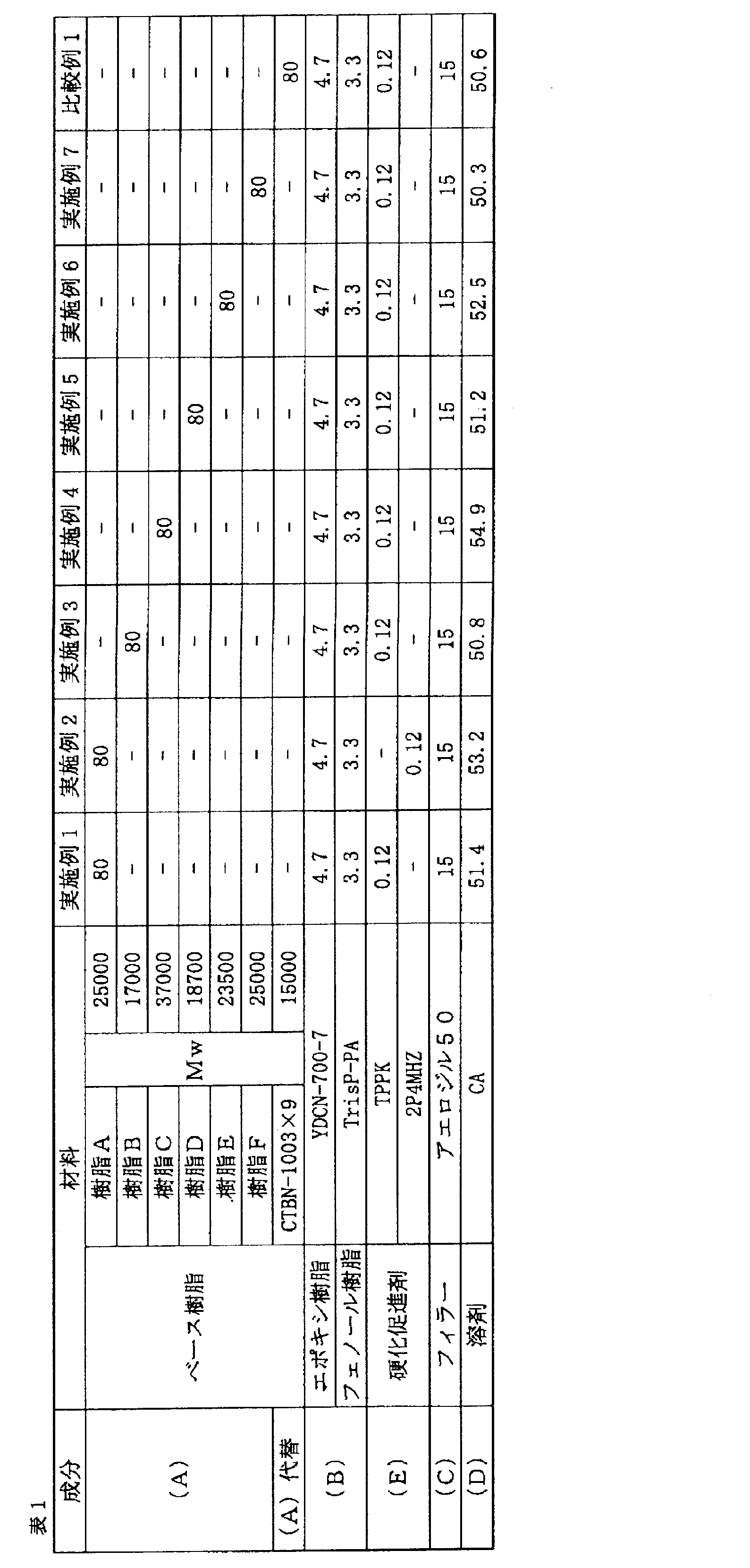
- Example 2 A resin paste was obtained in the same manner as in Example 1 except that the types and contents of the base resin, the curing accelerator, and the filler were changed as shown in Table 1.
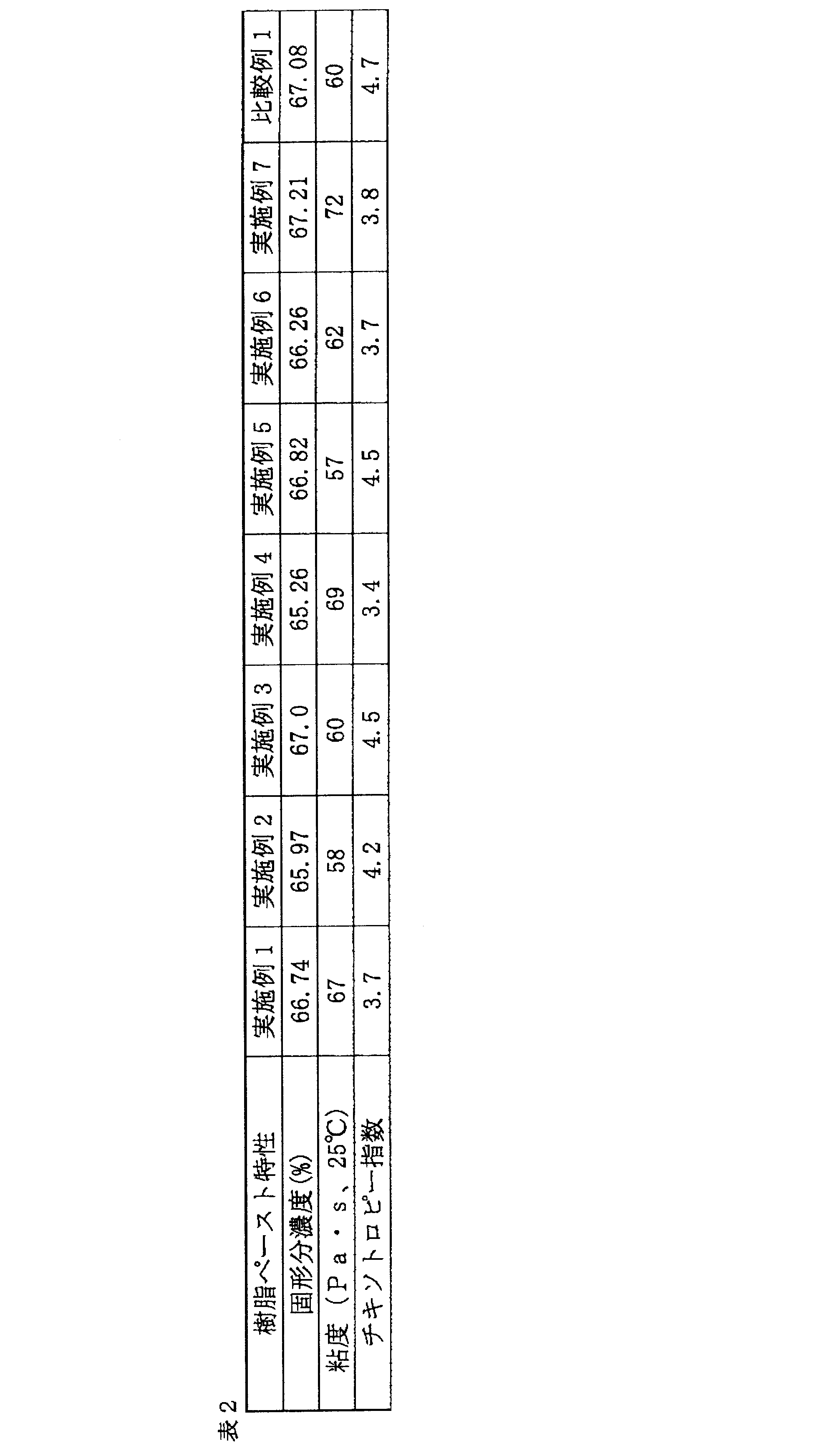
- Table 2 shows the solid content concentration, viscosity, and thixotropy index of the resin pastes obtained in Examples 2 to 7 and Comparative Example 1.
- each of the resin pastes of Examples 1 to 7 and Comparative Example 1 was performed under the condition that the set temperature for the B stage was changed to 140 ° C., 145 ° C., 150 ° C., 155 ° C., 160 ° C., 165 ° C. and 170 ° C.
- the shear strength (kgf / chip) at 180 ° C. was measured. The results are shown in Table 3.
- the resin pastes of Examples 1 to 7 and Comparative Example 1 were printed on a 42 alloy lead frame at 3 mm ⁇ 10 mm and a thickness of 100 ⁇ m.
- the B stage was set to 135 ° C. to make a B stage.
- the B-stage condition is that the temperature is raised from 40 ° C. to 135 ° C. in 30 minutes with a hot air dryer, dried at 135 ° C. for 30 minutes, and then lowered from 135 ° C. to 40 ° C. in 30 minutes.
- a coating film (die bonding layer) was formed. Thereafter, a transparent glass plate was pressure-bonded on the die bonding layer for 1 second on a 140 ° C. heating plate with a load of 5 kg. This was heat-pressed under conditions of 180 ° C. and 4 MPa for 90 seconds, and voids were visually evaluated according to the following criteria.
- each of the resin pastes of Examples 1 to 7 and Comparative Example 1 was performed under the condition that the set temperature for the B stage was changed to 140 ° C., 145 ° C., 150 ° C., 155 ° C., 160 ° C., 165 ° C. and 170 ° C. Similarly, the voids were visually evaluated. The results are shown in Table 3.
- A Void area is less than 5% with respect to the bonding area between the die bonding layer and the glass substrate.
- B Void area is 5% or more with respect to the bonding area between the die bonding layer and the glass substrate.
- a B-staging temperature range in which the adhesive strength was 0.1 MPa or more and the void evaluation was “A” was defined as the B-staging temperature tolerance. The results are shown in Table 3. It means that it is excellent, so that B stage-izing temperature tolerance is large.
- the adhesive strength is 0.1 MPa or more
- the subsequent assembly process that is, wire bonding and sealing can be performed even if the post-curing process is omitted.
- the package substrate for evaluation was prepared by applying for 1 second.
- Each of the obtained package substrates for evaluation was sealed using a transfer molding machine (transfer press manufactured by Towa Seiki Co., Ltd.) (sealing agent; product name: CEL-9240HF-SI (manufactured by Hitachi Chemical Co., Ltd.)) Sealing conditions; mold temperature: 180 ° C., pressure: 6.9 MPa, molding time: 90 seconds).
- the sealing material was heated and cured in a hot air dryer at 175 ° C. for 5 hours to obtain a BOC package for evaluation of 10.1 mm ⁇ 12.2 mm ⁇ 1.0 mmt.
- the obtained evaluation BOC package was subjected to moisture absorption under the conditions of 85 ° C./85% RH / 168 hours and 85 ° C./60% RH / 168 hours, respectively, and then the maximum surface temperature of the evaluation BOC package was 260 ° C. And passed through an IR reflow furnace (made by TAMURA) set to reach 3 times.
- SAT Scanning Automatic Tomography, HYE-FOCUS manufactured by Hitachi, Ltd.
- the reflow resistance was evaluated. The results are shown in Table 3.
- Level 1 No peeling of the die-bonding layer or bubbles in both conditions of 85 ° C./85% RH / 168 hours and 85 ° C./60% RH / 168 hours.
- Level 1 means better reflow resistance than Level 2.
- YDCN-700-7 Toto Kasei Co., Ltd., cresol novolac type epoxy resin (epoxy equivalent: 197-207 g / eq)
- TrisP-PA Honshu Chemical Industry Co., Ltd. (4- [4- [1,1-bis (4-hydroxyphenyl) ethyl] - ⁇ , ⁇ -dimethylbenzyl] phenol)
- TPPK Tokyo Chemical Industry Co., Ltd., Tetraphenylphosphonium Tetraphenylborate 2P4MHZ: Shikoku Chemical Industry Co., Ltd. (2-phenyl-4-methyl-5-hydroxymethylimidazole)
- Aerosil # 50 Nippon Aerosil Co., Ltd. (silica fine powder, average particle size 0.03 ⁇ m)
- CA carbitol acetate
- the resin paste for die bonding of the present invention is excellent in adhesive strength with a chip in a wide temperature range in B-stage, and can reduce voids between the chips, and in the solder reflow process, Excellent reflow resistance.
- the present invention it is possible to provide a die bonding resin paste that can be easily supplied and applied by a printing method to a substrate on which a semiconductor chip needs to be attached at a relatively low temperature.
Landscapes
- Chemical & Material Sciences (AREA)
- Organic Chemistry (AREA)
- Health & Medical Sciences (AREA)
- Chemical Kinetics & Catalysis (AREA)
- Medicinal Chemistry (AREA)
- Polymers & Plastics (AREA)
- Die Bonding (AREA)
- Adhesives Or Adhesive Processes (AREA)
- Compositions Of Macromolecular Compounds (AREA)
- Epoxy Resins (AREA)
Abstract
Description
本明細書の開示は、日本国特許出願2009-070531号(2009年3月23日出願)に含まれる主題に関し、これらの出願明細書を参照して全体的に本明細書に組み込むものとする。
カルボキシル基を有するブタジエンのポリマー(以下、成分(a1)と略す場合がある。)としては、ポリブタジエン構造及びカルボキシル基を有していれば特に限定されない。たとえば、ブタジエンから誘導されるポリブタジエン構造と、カルボキシル基を有する化合物との共重合体であってもよい。また、ブタジエンとアクリロニトリル等の他の重合性化合物とのコポリマーを主鎖とし、その末端の少なくとも一方にカルボキシル基を有するものであってもよい。印刷性、接着強度及び作業性の観点からは、成分(a1)の数平均分子量は500~10000であることが好ましく、1000~7000であることがより好ましい。本発明において、前記成分(a1)は、下記一般式(1)で表されるカルボキシル基を有するブタジエン-アクリロニトリル共重合体がより好ましい。

上記一般式(1)で表される化合物は、市販品として入手することも可能である。
エポキシ基を有する化合物(以下、成分(a2)と略す場合がある。)としては、特に限定されないが、例えば、エチレングリコールジグリシジルエーテル、ジエチレングリコールジグリシジルエーテル、プロピレングリコールジグリシジルエーテル、ジプロピレングリコールジグリシジルエーテル、グリセリントリグリシジルエーテルなどのグリシジルエーテル型エポキシ化合物;ダイマー酸などの多価カルボン酸とその無水物を原料とするグリシジルエステル型エポキシ化合物;脂肪族アミンを原料とするグリシジルアミン型エポキシ化合物等の脂肪族エポキシ化合物、ハイドロキノン、メチルハイドロキノン、ジメチルハイドロキノン、トリメチルハイドロキノン、レゾルシノール、メチルレゾルシノール、カテコール、メチルカテコール、ビフェノール、テトラメチルビフェノール、ジヒドロキシナフタレン、ジヒドロキシメチルナフタレン、ジヒドロキシジメチルナフタレン、ビス(4-ヒドロキシフェニル)ケトン、ビス(4-ヒドロキシ-3,5-ジメチルフェニル)ケトン、ビス(4-ヒドロキシ-3,5-ジクロロフェニル)ケトン、ビス(4-ヒドロキシフェニル)スルホン、ビス(4-ヒドロキシ-3,5-ジメチルフェニル)スルホン、ビス(4-ヒドロキシ-3,5-ジクロロフェニル)スルホン、ビス(4-ヒドロキシフェニル)ヘキサフルオロプロパン、ビス(4-ヒドロキシ-3,5-ジメチルフェニル)ヘキサフルオロプロパン、ビス(4-ヒドロキシ-3,5-ジクロロフェニル)ヘキサフルオロプロパン、ビス(4-ヒドロキシフェニル)ジメチルシラン、ビス(4-ヒドロキシ-3,5-ジメチルフェニル)ジメチルシラン、ビス(4-ヒドロキシ-3,5-ジクロロフェニル)ジメチルシラン、ビス(4-ヒドロキシフェニル)メタン、ビス(4-ヒドロキシ-3,5-ジクロロフェニル)メタン、ビス(4-ヒドロキシ-3,5-ジブロモフェニル)メタン、2,2-ビス(4-ヒドロキシフェニル)プロパン、2,2-ビス(4-ヒドロキシ-3,5-ジメチルフェニル)プロパン、2,2-ビス(4-ヒドロキシ-3,5-ジクロロフェニル)プロパン、2,2-ビス(4-ヒドロキシ-3-メチルフェニル)プロパン、2,2-ビス(4-ヒドロキシ-3-クロロフェニル)プロパン、ビス(4-ヒドロキシフェニル)エーテル、ビス(4-ヒドロキシ-3,5-ジメチルフェニル)エーテル、ビス(4-ヒドロキシ-3,5-ジクロロフェニル)エーテル、9,9-ビス(4-ヒドロキシフェニル)フルオレン、9,9-ビス(4-ヒドロキシ-3-メチルフェニル)フルオレン、9,9-ビス(4-ヒドロキシ-3-クロロフェニル)フルオレン、9,9-ビス(4-ヒドロキシ-3-ブロモフェニル)フルオレン、9,9-ビス(4-ヒドロキシ-3-フルオロフェニル)フルオレン、9,9-ビス(4-ヒドロキシ-3-メトキシフェニル)フルオレン、9,9-ビス(4-ヒドロキシ-3,5-ジメチルフェニル)フルオレン、9,9-ビス(4-ヒドロキシ-3,5-ジクロロフェニル)フルオレン、9,9-ビス(4-ヒドロキシ-3,5-ジブロモフェニル)フルオレンなどの1種以上とエピハロヒドリンとの縮合により得られるジグリシジル化合物等の芳香環を有するエポキシ化合物などの1分子内に2個のエポキシ基を有する化合物が挙げられる。

これらエポキシ基を有する化合物は、単独で、または2種以上を組み合わせて用いることができる。
ポリマー(A)は、成分(a1)と成分(a2)を反応させて得られる。この際の配合比は、成分(a1)の1カルボン酸当量に対して、成分(a2)のエポキシ当量は、接着強度を考慮すると0.01以上、アウトガス発生による剥離のし難さを考慮すると10以下であることが好ましく、0.1~2であることがより好ましく、0.25~1であることが特に好ましい。
また、ポリマー(A)の酸価は、10~25mgKOH/gであることが好ましく、15~23mgKOH/gであることがより好ましい。
酸価が10~25mgKOH/gであると、樹脂ペーストにした時の作業性をより向上させることができる。
上記ポリマー(A)の酸価は、以下の方法により測定することができる。まず、ポリマー(A)の樹脂溶液を約1gを精秤した後、その樹脂溶液にアセトンを30g添加し、樹脂溶液を均一に溶解する。次いで、指示薬であるフェノールフタレインをその溶液に適量添加して、0.1NのKOH水溶液を用いて滴定を行う。そして、滴定結果より以下の式(3);
A=10×Vf×56.1/(Wp×I)・・・・・(3)
により酸価を算出する。なお、式(I)中、Aは酸価(mgKOH/g)を示し、Vfはフェノールフタレインの滴定量(mL)を示し、Wpはポリマー(A)の樹脂溶液重量(g)を示し、Iはポリマー(A)の樹脂溶液の不揮発分の割合(質量%)を示す。
熱硬化性樹脂(B)としては、特に限定されないが、たとえば、エポキシ樹脂、フェノール樹脂、1分子中に少なくとも2個の熱硬化性イミド基を有するイミド化合物等が挙げられる。これらは、1種を単独で又は2種以上を組み合わせて用いられる。
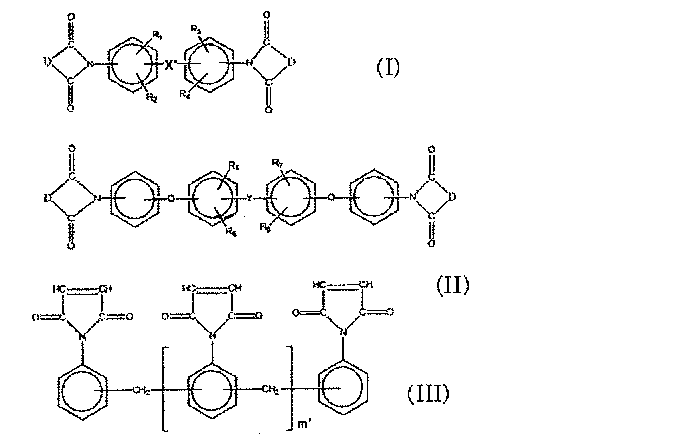
イミド化合物を用いる場合の含有量は、樹脂ペーストの保管安定性を考慮すると、ポリマー(A)100重量部に対して、100重量部未満であることがより好ましい。
フィラー(C)としては、以下の例には限定されないが、たとえば、銀粉、金粉、銅粉等の導電性フィラー;シリカ、アルミナ、チタニア、ガラス、酸化鉄、セラミック等の無機物質フィラー;等が挙げられる。これらは1種を単独で又は2種以上を組み合わせて用いられる。
本発明の樹脂ペーストは、溶剤(D)を含有してもよい。溶剤(D)は、フィラーを均一に混練または分散できる有機溶剤の中から選択することが好ましい。印刷時の有機溶剤の揮散防止及びBステージ化における乾燥性を考慮して、沸点(大気圧)が100℃以上250℃未満の有機溶剤を選ぶことが好ましい。
本発明の樹脂ペーストは、硬化促進剤(E)を含有することが好ましい。硬化促進剤(E)は、熱硬化性樹脂(B)の硬化を促進させることできる。特に熱硬化性樹脂(B)としてエポキシ樹脂を用いる場合に特に有効である。
更に、本発明の樹脂ペーストには、必要に応じて、消泡剤、破泡剤、抑泡剤、シラン系カップリング剤、チタン系カップリング剤、ノニオン系界面活性剤、フッ素系界面活性剤、シリコーン系可塑剤等の各種添加剤を添加することもできる。
以下、半導体装置の製造方法について説明する。
これらは封止樹脂207により封止されており、外部に突き出たリードフレームの端部には外部めっき208が施されている。
成分(a1)としてCTBNX-1300×9(宇部興産株式会社製、カルボキシル基含有アクリロニトリルポリブタジエン共重合体の商品名、アクリロニトリルの含有量は約17重量%)を100重量部及び成分(a2)としてEXA-830CRP(DIC株式会社製、一般式(2)において、Xが-CH2-であり、R1及びR2が水素原子であり、n及びmが4であるビスフェノールF型エポキシ化合物)を10重量部秤取しフラスコに加えた。(カルボン酸当量:エポキシ当量=1:1)これを145℃で加熱しながら1時間攪拌させ、ポリマー(A)として樹脂Aを得た。粘度450Pa・sであった。重量平均分子量(Mw)は25000であった。
撹拌時間を1時間から30分に変更した以外は、合成例1と同様にして樹脂Bを得た。粘度188Pa・sであった。重量平均分子量(Mw)は17000であった。
撹拌時間を1時間から1時間45分に変更した以外は、合成例1と同様にして樹脂Cを得た。粘度962Pa・sであった。重量平均分子量(Mw)は37000であった。
成分(a2)であるEXA-830CRPの量を、10重量部から2.5重量部に変更した以外は、実施例1と同様にして樹脂Dを得た(カルボン酸当量:エポキシ当量=1:0.25)。粘度212Pa・sであった。重量平均分子量(Mw)は18700であった。
成分(a2)であるEXA-830CRPを10重量部から100重量部に変更した以外は、実施例1と同様にして樹脂Eを得た(カルボン酸当量:エポキシ当量=1:10)。粘度472Pa・sであった。重量平均分子量(Mw)は23500であった。
成分(a2)を、EXA-830CRP10重量部からR1710(ビスフェノールAD型、三井化学株式会社製)10重量部に変更した以外は、実施例1と同様にして樹脂Fを得た(カルボン酸当量:エポキシ当量=1:1)。粘度412Pa・sであった。重量平均分子量(Mw)は25000であった。
検出器:日立 L-3300 RI
データ処理機:ATT
カラム:Gelpack GL-R440+Gelpack GL-R450+Gelpack GL-R400M
カラムサイズ:10.7mmφ×300mm
溶媒:THF
試料濃度:120mg/5ml
注入量:200μl
圧力:34kgf/cm2
流量:2.05ml/min
(実施例1)
ポリマー(A)(ベース樹脂)として、樹脂Aを80重量部秤取し、これを混練機に入れた。ここに、熱硬化性樹脂(B)として、エポキシ樹脂(商品名:YDCN-700-7、東都化成株式会社社製)4.7重量部及びフェノール樹脂(商品名:TrisP-PA-MF、本州化学工業株式会社製)3.3重量部を、溶剤(D)であるカルビトールアセテート(CA)40重量部で溶解した溶液(熱硬化性樹脂の固形分濃度は約40重量%)と、硬化促進剤(商品名:TPPK、東京化成工業株式会社製)0.12重量部を加え、混合した。次に、フィラー(C)としてシリカ微粉末(商品名:アエロジル#50、日本アエロジル株式会社製)を15重量部、さらにカルビトールアセテート(CA)を11.4重量部加え1時間撹拌・混練し、樹脂ペーストを得た。実施例1で得られた樹脂ペーストの固形分濃度、粘度及びチキソトロピー指数を表2に示す。
ベース樹脂、硬化促進剤、フィラーの種類および含有量を表1のように替えた以外は、実施例1と同様にして樹脂ペーストを得た。実施例2~7及び比較例1で得られた樹脂ペーストの固形分濃度、粘度及びチキソトロピー指数を表2に示す。
実施例1~7、及び比較例1の樹脂ペーストを、42アロイリードフレーム上に100μm厚で印刷した。次に、Bステージ化温度を135℃に設定してBステージ化した。Bステージ化条件としては、熱風乾燥機で40℃から135℃まで30分間で昇温し、135℃で30分間乾燥後、135℃から40℃まで30分間で降温させることによって、Bステージ化状態の塗膜(ダイボンディング層)を形成した。その後、ダイボンディング層上に5×5mmのシリコンチップ(厚さ0.5mm)を140℃の熱盤上で5kgの荷重を掛けて1秒間圧着させた。これを、自動接着力試験機(商品名:serie-4000、デイジ社製)を用い、180℃におけるせん断強さ(kgf/チップ)を測定した。
実施例1~7、及び比較例1の樹脂ペーストを、42アロイリードフレーム上に3mm×10mm、厚さ100μmで印刷した。次ぎに、Bステージ化温度を135℃に設定してBステージ化した。Bステージ化条件としては、熱風乾燥機で40℃から135℃まで30分間で昇温し、135℃で30分間乾燥後、135℃から40℃まで30分間で降温させることによって、Bステージ化状態の塗膜(ダイボンディング層)を形成した。その後、ダイボンディング層上に透明なガラスプレートを、140℃の熱盤上で5kgの荷重を掛けて1秒間圧着させた。これを、180℃、4MPaで90秒間の条件で加熱圧着させて、以下の基準によりボイドを目視で評価した。
B:ダイボンディング層とガラス基板の接着面積に対して、ボイド面積が5%以上
[Bステージ化温度裕度]
接着強度が0.1MPa以上で、且つ、ボイドの評価が「A」となるBステージ化温度範囲をBステージ化温度裕度とした。結果を表3に示す。Bステージ化温度裕度が大きい程優れることを意味する。
樹脂ペーストを42アロイリードフレーム上に100μmm厚で印刷し、熱風乾燥機で40℃から160℃まで30分間で昇温し、160℃で30分間、160℃から40℃まで30分間で降温させることによって乾燥し、Bステージ化状態の塗膜(ダイボンディング層)を形成した。その後、ダイボンディング層上に5×5mmのシリコンチップ(厚さ0.5mm)を140℃の熱盤上で5kgの荷重を掛けて1秒間圧着させた。次いで、180℃の熱風乾燥機で60分間加熱し、後硬化させた。これを、自動接着力試験機(商品名:serie-4000、デイジ社製)を用い、250℃におけるせん断強さ(kgf/チップ)を測定し、250℃における熱時ダイシェア強度とした。
ソルダーレジスト(商品名:AUS-308、太陽インキ製造(株)社製)が塗布された有機基板上に、印刷機とメタルマスク(マスク形状9.0×4.0×120um×2箇所)を用い、実施例1~7及び比較例1の樹脂ペーストをそれぞれ印刷した。次に、実施例1~7及び比較例1の樹脂ペーストを印刷したそれぞれの有機基板において、熱風乾燥機により40℃からBステージ化温度裕度における最下限温度(例えば、実施例1の樹脂ペーストでは155℃)まで30分間で昇温し、Bステージ化温度裕度における最下限温度で30分間保持し、その後40℃まで30分間で降温させることによって乾燥し、Bステージ化状態の塗膜(ダイボンディング層)を形成した。次に、ダイボンディング層上に熱酸化膜付きシリコンチップ(8.8mm×8.8mm×280umt)を日立製作所製チップマウンタ(CM-110)を用いて140℃の熱盤上で6kgの荷重を掛けて1秒間圧着して評価用パッケージ基板を作成した。得られたそれぞれの評価用パッケージ基板を、トランスファ成形機(藤和精機製トランスファプレス)を用いて封止した(封止剤;商品名:CEL-9240HF-SI(日立化成工業(株)製、)封止条件;金型温度:180℃、圧力:6.9MPa、成形時間:90秒間)。その後、175℃の熱風乾燥機中で5時間、封止材を加熱硬化して、10.1mm×12.2mm×1.0mmtの評価用BOCパッケージを得た。
TrisP-PA:本州化学工業株式会社、(4-〔4-[1,1-ビス(4-ヒドロキシフェニル)エチル]-α,α-ジメチルベンジル〕フェノール)
TPPK:東京化成工業株式会社、テトラフェニルホスホニウムテトラフェニルボラート2P4MHZ:四国化成工業株式会社、(2-フェニル-4-メチル-5-ヒドロキシメチルイミダゾール)
アエロジル#50:日本アエロジル株式会社、(シリカの微粉末、平均粒径0.03μm)
CA:カルビトールアセテート

4 ダイボンディング層
6 半導体チップ
8 配線パターン
10 絶縁層
12 はんだボール
14 ワイヤ
16 封止材
100 半導体装置
101 基板
102 メタルマスク
103 スキージ
104 ダイボンディング用樹脂ペースト
105 ダイボンディング層(Bステージ化状態)
106 熱源
107 チップ
108 ダイボンディング層(完全硬化状態)
109 ワイヤ
110 金型
111 押し出し機
112 封止材
201 シリコンチップ
202 ダイボンディング用樹脂ペースト
203 リードフレーム
204 Alパッド
205 Agめっき
206 金線
207 封止樹脂
208 外部めっき
Claims (8)
- カルボキシル基を有するブタジエンのポリマー(a1)とエポキシ基を有する化合物(a2)を反応させて得られるポリマー(A)、熱硬化性樹脂(B)及びフィラー(C)を含む、ダイボンディング用樹脂ペースト。
- さらに溶剤(D)を含む請求項1に記載のダイボンディング用樹脂ペースト。
- さらに硬化促進剤(E)を含む請求項1に記載のダイボンディング用樹脂ペースト。
- 前記カルボキシル基を有するブタジエンのポリマー(a1)とエポキシ基を有する化合物(a2)を反応させて得られるポリマー(A)の重量平均分子量が、15,000~70,000である請求項1に記載のダイボンディング用樹脂ペースト。
- (1)基板上に、請求項1~3のいずれか一項に記載のダイボンディング用樹脂ペーストを塗布する工程、(2)前記樹脂ペーストをBステージ化する工程、(3)Bステージ化した前記樹脂ペーストに半導体チップを搭載する工程と、を含む半導体装置の製造方法。
- 請求項5に記載の半導体装置の製造方法により得られる半導体装置。
- (1)基板上に、請求項1~3のいずれか一項に記載のダイボンディング用樹脂ペーストを塗布する工程、(2)前記樹脂ペーストに半導体チップを搭載する工程、(3)前記半導体チップを封止剤により封止する工程と、を含む半導体装置の製造方法。
- 請求項7に記載の半導体装置の製造方法により得られる半導体装置。
Priority Applications (3)
| Application Number | Priority Date | Filing Date | Title |
|---|---|---|---|
| KR1020117015583A KR20120010220A (ko) | 2009-03-23 | 2010-03-10 | 다이본딩용 수지 페이스트, 그것을 이용한 반도체 장치의 제조 방법, 및 반도체 장치 |
| CN2010800041529A CN102272908A (zh) | 2009-03-23 | 2010-03-10 | 晶片接合用树脂浆料、使用该浆料的半导体装置的制造方法及半导体装置 |
| JP2011505970A JPWO2010110069A1 (ja) | 2009-03-23 | 2010-03-10 | ダイボンディング用樹脂ペースト、それを用いた半導体装置の製造方法、及び半導体装置 |
Applications Claiming Priority (2)
| Application Number | Priority Date | Filing Date | Title |
|---|---|---|---|
| JP2009070531 | 2009-03-23 | ||
| JP2009-070531 | 2009-03-23 |
Publications (1)
| Publication Number | Publication Date |
|---|---|
| WO2010110069A1 true WO2010110069A1 (ja) | 2010-09-30 |
Family
ID=42780762
Family Applications (1)
| Application Number | Title | Priority Date | Filing Date |
|---|---|---|---|
| PCT/JP2010/054027 Ceased WO2010110069A1 (ja) | 2009-03-23 | 2010-03-10 | ダイボンディング用樹脂ペースト、それを用いた半導体装置の製造方法、及び半導体装置 |
Country Status (5)
| Country | Link |
|---|---|
| JP (1) | JPWO2010110069A1 (ja) |
| KR (1) | KR20120010220A (ja) |
| CN (1) | CN102272908A (ja) |
| TW (1) | TW201038699A (ja) |
| WO (1) | WO2010110069A1 (ja) |
Cited By (3)
| Publication number | Priority date | Publication date | Assignee | Title |
|---|---|---|---|---|
| JP2018172695A (ja) * | 2016-06-02 | 2018-11-08 | 日立化成株式会社 | 樹脂組成物及び積層体の製造方法 |
| US11024598B2 (en) | 2016-08-22 | 2021-06-01 | Senju Metal Industry Co., Ltd. | Metallic sintered bonding body and die bonding method |
| WO2025079497A1 (ja) * | 2023-10-12 | 2025-04-17 | セントラル硝子株式会社 | 半導体デバイスの製造方法 |
Families Citing this family (6)
| Publication number | Priority date | Publication date | Assignee | Title |
|---|---|---|---|---|
| CN107709502B (zh) * | 2015-06-29 | 2021-06-15 | 拓自达电线株式会社 | 散热材料粘接用组合物、带粘接剂的散热材料、嵌入基板和其制造方法 |
| US9704820B1 (en) * | 2016-02-26 | 2017-07-11 | Taiwan Semiconductor Manufacturing Company Ltd. | Semiconductor manufacturing method and associated semiconductor manufacturing system |
| CN107541168A (zh) * | 2017-07-31 | 2018-01-05 | 常州聚盛节能工程有限公司 | 一种建筑结构胶及其制备方法 |
| WO2020217394A1 (ja) | 2019-04-25 | 2020-10-29 | 日立化成株式会社 | ドルメン構造を有する半導体装置及びその製造方法、並びに、支持片形成用積層フィルム及びその製造方法 |
| WO2020217404A1 (ja) * | 2019-04-25 | 2020-10-29 | 日立化成株式会社 | ドルメン構造を有する半導体装置及びその製造方法 |
| WO2026050296A1 (en) * | 2024-08-26 | 2026-03-05 | Henkel Ag & Co. Kgaa | B-stage thermally conductive adhesive |
Citations (2)
| Publication number | Priority date | Publication date | Assignee | Title |
|---|---|---|---|---|
| JP2002526618A (ja) * | 1998-10-06 | 2002-08-20 | ヘンケル・テロソン・ゲゼルシャフト・ミット・ベシュレンクテル・ハフツング | 耐衝撃性エポキシ樹脂組成物 |
| JP2009019171A (ja) * | 2007-07-13 | 2009-01-29 | Kyocera Chemical Corp | ダイボンディングペースト |
Family Cites Families (2)
| Publication number | Priority date | Publication date | Assignee | Title |
|---|---|---|---|---|
| TWI299748B (en) * | 2000-02-15 | 2008-08-11 | Hitachi Chemical Co Ltd | Adhesive composition, its manufacturing method, and adhesive film, substrate for carrying a semiconductor device and semiconductor device using such adhesive composition |
| JP2005281673A (ja) * | 2004-03-02 | 2005-10-13 | Tamura Kaken Co Ltd | 熱硬化性樹脂組成物、樹脂フィルムおよび製品 |
-
2010
- 2010-03-10 JP JP2011505970A patent/JPWO2010110069A1/ja active Pending
- 2010-03-10 WO PCT/JP2010/054027 patent/WO2010110069A1/ja not_active Ceased
- 2010-03-10 KR KR1020117015583A patent/KR20120010220A/ko not_active Withdrawn
- 2010-03-10 CN CN2010800041529A patent/CN102272908A/zh active Pending
- 2010-03-12 TW TW099107287A patent/TW201038699A/zh unknown
Patent Citations (2)
| Publication number | Priority date | Publication date | Assignee | Title |
|---|---|---|---|---|
| JP2002526618A (ja) * | 1998-10-06 | 2002-08-20 | ヘンケル・テロソン・ゲゼルシャフト・ミット・ベシュレンクテル・ハフツング | 耐衝撃性エポキシ樹脂組成物 |
| JP2009019171A (ja) * | 2007-07-13 | 2009-01-29 | Kyocera Chemical Corp | ダイボンディングペースト |
Cited By (3)
| Publication number | Priority date | Publication date | Assignee | Title |
|---|---|---|---|---|
| JP2018172695A (ja) * | 2016-06-02 | 2018-11-08 | 日立化成株式会社 | 樹脂組成物及び積層体の製造方法 |
| US11024598B2 (en) | 2016-08-22 | 2021-06-01 | Senju Metal Industry Co., Ltd. | Metallic sintered bonding body and die bonding method |
| WO2025079497A1 (ja) * | 2023-10-12 | 2025-04-17 | セントラル硝子株式会社 | 半導体デバイスの製造方法 |
Also Published As
| Publication number | Publication date |
|---|---|
| TW201038699A (en) | 2010-11-01 |
| KR20120010220A (ko) | 2012-02-02 |
| JPWO2010110069A1 (ja) | 2012-09-27 |
| CN102272908A (zh) | 2011-12-07 |
Similar Documents
| Publication | Publication Date | Title |
|---|---|---|
| JP5360124B2 (ja) | ダイボンディング用樹脂ペーストおよびその用途 | |
| WO2010110069A1 (ja) | ダイボンディング用樹脂ペースト、それを用いた半導体装置の製造方法、及び半導体装置 | |
| CN103031091A (zh) | 芯片接合用树脂糊、半导体装置的制造方法和半导体装置 | |
| JP5225853B2 (ja) | ダイボンディング用樹脂ペースト、半導体装置の製造方法及び半導体装置 | |
| JP5157938B2 (ja) | ダイボンディング用樹脂ペースト、該樹脂ペーストを用いた半導体装置の製造方法、および該製造方法により得られる半導体装置 | |
| JP4816876B2 (ja) | ダイボンディング用樹脂ペーストおよび半導体装置の製造方法 | |
| JPWO2010070947A1 (ja) | ダイボンディング用樹脂ペースト、半導体装置の製造方法及び半導体装置 | |
| JP2008277803A (ja) | ダイボンディング用樹脂ペースト組成物、それを用いた半導体装置の製造方法及び半導体装置 | |
| JP5130682B2 (ja) | ダイボンディング用樹脂ペースト、該樹脂ペーストを用いた半導体装置の製造方法、および該製造方法により得られる半導体装置 | |
| JP2008270717A (ja) | ダイボンディング用樹脂ペースト組成物、それを用いた半導体装置の製造方法及び半導体装置 | |
| JP2013170254A (ja) | ダイボンディング用樹脂ペースト、半導体装置の製造方法及び半導体装置 | |
| JP2007142117A (ja) | ダイボンディングペーストおよびそれを用いた半導体装置 | |
| JP2008112972A (ja) | ダイボンディング用樹脂ペースト、半導体装置の製造方法及び半導体装置 | |
| JP2007110099A (ja) | ダイボンディング材及びダイボンディング材用樹脂ペースト | |
| JP2006342300A (ja) | 接着フィルム及びそれを用いた半導体装置 | |
| JP2009197068A (ja) | 液状樹脂組成物および半導体装置 | |
| CN104025272A (zh) | 模片结合剂 |
Legal Events
| Date | Code | Title | Description |
|---|---|---|---|
| WWE | Wipo information: entry into national phase |
Ref document number: 201080004152.9 Country of ref document: CN |
|
| 121 | Ep: the epo has been informed by wipo that ep was designated in this application |
Ref document number: 10755869 Country of ref document: EP Kind code of ref document: A1 |
|
| WWE | Wipo information: entry into national phase |
Ref document number: 2011505970 Country of ref document: JP |
|
| ENP | Entry into the national phase |
Ref document number: 20117015583 Country of ref document: KR Kind code of ref document: A |
|
| NENP | Non-entry into the national phase |
Ref country code: DE |
|
| 122 | Ep: pct application non-entry in european phase |
Ref document number: 10755869 Country of ref document: EP Kind code of ref document: A1 |