WO2010106576A1 - 不揮発性液晶表示装置および、不揮発性液晶表示装置の表示方法 - Google Patents
不揮発性液晶表示装置および、不揮発性液晶表示装置の表示方法 Download PDFInfo
- Publication number
- WO2010106576A1 WO2010106576A1 PCT/JP2009/001215 JP2009001215W WO2010106576A1 WO 2010106576 A1 WO2010106576 A1 WO 2010106576A1 JP 2009001215 W JP2009001215 W JP 2009001215W WO 2010106576 A1 WO2010106576 A1 WO 2010106576A1
- Authority
- WO
- WIPO (PCT)
- Prior art keywords
- liquid crystal
- signal line
- crystal display
- selection voltage
- display device
- Prior art date
- Legal status (The legal status is an assumption and is not a legal conclusion. Google has not performed a legal analysis and makes no representation as to the accuracy of the status listed.)
- Ceased
Links
Images



Classifications
-
- G—PHYSICS
- G09—EDUCATION; CRYPTOGRAPHY; DISPLAY; ADVERTISING; SEALS
- G09G—ARRANGEMENTS OR CIRCUITS FOR CONTROL OF INDICATING DEVICES USING STATIC MEANS TO PRESENT VARIABLE INFORMATION
- G09G3/00—Control arrangements or circuits, of interest only in connection with visual indicators other than cathode-ray tubes
- G09G3/20—Control arrangements or circuits, of interest only in connection with visual indicators other than cathode-ray tubes for presentation of an assembly of a number of characters, e.g. a page, by composing the assembly by combination of individual elements arranged in a matrix no fixed position being assigned to or needed to be assigned to the individual characters or partial characters
- G09G3/34—Control arrangements or circuits, of interest only in connection with visual indicators other than cathode-ray tubes for presentation of an assembly of a number of characters, e.g. a page, by composing the assembly by combination of individual elements arranged in a matrix no fixed position being assigned to or needed to be assigned to the individual characters or partial characters by control of light from an independent source
- G09G3/36—Control arrangements or circuits, of interest only in connection with visual indicators other than cathode-ray tubes for presentation of an assembly of a number of characters, e.g. a page, by composing the assembly by combination of individual elements arranged in a matrix no fixed position being assigned to or needed to be assigned to the individual characters or partial characters by control of light from an independent source using liquid crystals
- G09G3/3611—Control of matrices with row and column drivers
- G09G3/3674—Details of drivers for scan electrodes
- G09G3/3681—Details of drivers for scan electrodes suitable for passive matrices only
-
- G—PHYSICS
- G02—OPTICS
- G02F—OPTICAL DEVICES OR ARRANGEMENTS FOR THE CONTROL OF LIGHT BY MODIFICATION OF THE OPTICAL PROPERTIES OF THE MEDIA OF THE ELEMENTS INVOLVED THEREIN; NON-LINEAR OPTICS; FREQUENCY-CHANGING OF LIGHT; OPTICAL LOGIC ELEMENTS; OPTICAL ANALOGUE/DIGITAL CONVERTERS
- G02F1/00—Devices or arrangements for the control of the intensity, colour, phase, polarisation or direction of light arriving from an independent light source, e.g. switching, gating or modulating; Non-linear optics
- G02F1/01—Devices or arrangements for the control of the intensity, colour, phase, polarisation or direction of light arriving from an independent light source, e.g. switching, gating or modulating; Non-linear optics for the control of the intensity, phase, polarisation or colour
- G02F1/13—Devices or arrangements for the control of the intensity, colour, phase, polarisation or direction of light arriving from an independent light source, e.g. switching, gating or modulating; Non-linear optics for the control of the intensity, phase, polarisation or colour based on liquid crystals, e.g. single liquid crystal display cells
- G02F1/137—Devices or arrangements for the control of the intensity, colour, phase, polarisation or direction of light arriving from an independent light source, e.g. switching, gating or modulating; Non-linear optics for the control of the intensity, phase, polarisation or colour based on liquid crystals, e.g. single liquid crystal display cells characterised by the electro-optical or magneto-optical effect, e.g. field-induced phase transition, orientation effect, guest-host interaction or dynamic scattering
- G02F1/13718—Devices or arrangements for the control of the intensity, colour, phase, polarisation or direction of light arriving from an independent light source, e.g. switching, gating or modulating; Non-linear optics for the control of the intensity, phase, polarisation or colour based on liquid crystals, e.g. single liquid crystal display cells characterised by the electro-optical or magneto-optical effect, e.g. field-induced phase transition, orientation effect, guest-host interaction or dynamic scattering based on a change of the texture state of a cholesteric liquid crystal
-
- G—PHYSICS
- G09—EDUCATION; CRYPTOGRAPHY; DISPLAY; ADVERTISING; SEALS
- G09G—ARRANGEMENTS OR CIRCUITS FOR CONTROL OF INDICATING DEVICES USING STATIC MEANS TO PRESENT VARIABLE INFORMATION
- G09G3/00—Control arrangements or circuits, of interest only in connection with visual indicators other than cathode-ray tubes
- G09G3/20—Control arrangements or circuits, of interest only in connection with visual indicators other than cathode-ray tubes for presentation of an assembly of a number of characters, e.g. a page, by composing the assembly by combination of individual elements arranged in a matrix no fixed position being assigned to or needed to be assigned to the individual characters or partial characters
- G09G3/34—Control arrangements or circuits, of interest only in connection with visual indicators other than cathode-ray tubes for presentation of an assembly of a number of characters, e.g. a page, by composing the assembly by combination of individual elements arranged in a matrix no fixed position being assigned to or needed to be assigned to the individual characters or partial characters by control of light from an independent source
- G09G3/36—Control arrangements or circuits, of interest only in connection with visual indicators other than cathode-ray tubes for presentation of an assembly of a number of characters, e.g. a page, by composing the assembly by combination of individual elements arranged in a matrix no fixed position being assigned to or needed to be assigned to the individual characters or partial characters by control of light from an independent source using liquid crystals
- G09G3/3611—Control of matrices with row and column drivers
- G09G3/3622—Control of matrices with row and column drivers using a passive matrix
- G09G3/3629—Control of matrices with row and column drivers using a passive matrix using liquid crystals having memory effects, e.g. ferroelectric liquid crystals
Definitions
- the present invention relates to a liquid crystal display device that displays an image by driving a liquid crystal, and more particularly to a nonvolatile liquid crystal display device having a memory property that can be used for electronic paper and a display method of the nonvolatile liquid crystal display device. .
- a liquid crystal compound is filled between a scanning signal line group and a data signal line group constituting a matrix, and a large number of pixels are formed at intersections of the scanning signal line group and the data signal line group to store image information.
- Liquid crystal display devices that perform display are well known. Among them, for example, a cholesteric liquid crystal display device used for electronic paper or the like has an advantage of having a memory property that display contents are not lost even when the power is turned off.
- FIG. 4 is a diagram for explaining the state of the cholesteric liquid crystal.
- the cholesteric liquid crystal display device controls display according to the alignment state of the liquid crystal molecules.
- a cholesteric liquid crystal display device displays image information using the phenomenon as described above (see, for example, Patent Document 1). Japanese Patent Publication No. 2001-228459
- FIG. 5 is a diagram for explaining a problem (part 1) of the prior art.
- FIG. 5A is a diagram for explaining a problem (part 2) of the conventional technique.
- the present invention has been made in view of the above-described situation, and in a cholesteric liquid crystal controlled by a simple matrix, a non-volatile liquid crystal display device capable of stabilizing the liquid crystal operation, that is, stabilizing the hue of the cholesteric liquid crystal, and
- An object of the present invention is to provide a display method for a nonvolatile liquid crystal display device.
- the non-volatile liquid crystal display device of the present invention is arranged at a position where the scanning signal line group and the data signal line group intersecting the scanning line signal group intersect the signal line group.
- a liquid crystal display panel including a non-volatile liquid crystal compound as a liquid crystal layer, scanning signal line driving means for sequentially driving the scanning signal line group, and a selection voltage for the scanning signal line driving means.
- Control means for supplying a non-selection voltage is provided. The control means supplies the non-selection voltage to each of all the scanning signal lines constituting the scanning signal line group before and after supplying the selection voltage for a predetermined period. To do.
- the nonvolatile liquid crystal display device of the present invention in the partial rewriting in which the control unit scans only the scanning signal line whose display content is changed, the scanning signal line to be subjected to the partial rewriting, It is preferable that the non-selection voltage is supplied during a predetermined period after the selection voltage is supplied.
- the liquid crystal layer is preferably a cholesteric liquid crystal layer.
- the display method of the present invention is arranged at a position where the scanning signal line group, the data signal line group intersecting the scanning line signal group, and the signal line group intersect.
- a liquid crystal display panel including a plurality of pixel circuits and containing a non-volatile liquid crystal compound as a liquid crystal layer; scanning signal line driving means for sequentially driving the scanning signal line group; and a selection voltage not applied to the scanning signal line driving means.
- a display method of a non-volatile liquid crystal display device comprising a control means for supplying a selection voltage, wherein the control means applies the selection voltage to each of all scanning signal lines constituting the scanning signal line group.
- the non-selection voltage is supplied during a predetermined period before and after supply.
- the control unit when the control unit performs partial rewriting in which only scanning signal lines whose display contents are changed are scanned, the control signal is changed to the scanning signal line to be partially rewritten.
- the liquid crystal layer is preferably a cholesteric liquid crystal layer.
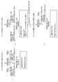
- FIG. 1 is a diagram for explaining a first embodiment to which the present invention is applied.
- a nonvolatile liquid crystal display device to which the present invention is applied includes a scanning signal line group, a data signal line group intersecting the scanning line signal group, and a plurality of pixel circuits arranged at positions where these signal line groups intersect.
- a liquid crystal display panel containing a non-volatile liquid crystal compound such as cholesteric liquid crystal as a liquid crystal layer The liquid crystal display panel can display an image by sequentially driving the scanning signal line groups.
- cholesteric liquid crystals have a characteristic that maintains the liquid crystal state even when the applied voltage is cut off.
- matrix control is performed with two types of selection voltage (voltage that becomes focal conic) and non-selection voltage (voltage that does not change the state). Do.
- the voltage applied to the liquid crystal of line A in FIG. 5 is a relatively long state in which the non-selection voltage after passing through the scanning line is applied.
- the liquid crystal is stabilized and a dark color display is possible.
- the voltage applied to the liquid crystal of the line D in FIG. 5 is relatively short when the non-selection voltage after passing through the scanning line is applied. Is not stable and the display is light.
- the non-selection voltage is supplied to each of all the scanning signal lines constituting the scanning signal line group before and after the selection voltage is supplied (see FIG. 1C).
- the selection voltage is applied for an arbitrary time, the focal conic state is obtained.
- the liquid crystal state can be stabilized by applying the non-selection voltage before and after the selection voltage. In other words, the homeotropic state is entered while the non-selection voltage is applied, and the state is close to the focal conic state.
- an image is displayed on a liquid crystal display panel containing cholesteric liquid crystal or the like, that is, when a non-selection voltage is applied for a certain period of time before and after the selection voltage is applied, a stable color image can be displayed. Reduce unevenness in the panel surface.
- FIG. 2 is a diagram for explaining a second embodiment to which the present invention is applied.
- a nonvolatile liquid crystal display device to which the present invention is applied includes a scanning signal line that is a target of partial rewriting when scanning is performed only on scanning signal lines whose display contents are changed.
- the non-selection voltage is supplied in a predetermined period after the selection voltage is supplied.
- the voltage applied to the liquid crystal of line B in FIG. 6 is such that the non-selection voltage applied after passing through the scanning line continues for a relatively long time.
- the liquid crystal is stabilized and a dark color display is possible.
- the voltage applied to the liquid crystal of line C in FIG. 6 is relatively short when the non-selection voltage after passing through the scanning line is applied. Is not stable and the display is light.
- the non-selection voltage is supplied to the scanning signal line to be partially rewritten in a predetermined period after the selection voltage is supplied (see FIG. 2C).
- a selection voltage is applied for an arbitrary time
- a focal conic state is achieved.
- the liquid crystal state can be stabilized. That is, the homeotropic state is entered while the non-selection voltage is applied, and the state is close to the focal conic state.
- FIG. 3 is a flowchart showing the flow of display control processing in the second embodiment to which the present invention is applied.
- step S301 when the partial rewrite ON sequence is started in step S301, a counter that counts display time is started together with the start of the partial rewrite sequence in step S302, and image display is executed in step S303.
- step S305 When the partial rewriting is completed in step S304, it is determined in step S305 whether or not the counter started in step S302 is 300 milliseconds (ms) or more. This is because in order for the liquid crystal state to be stable, a total time of about 300 milliseconds is required for applying the non-selection voltage before and after the scanning line passes.
- the time for which the non-selection voltage is applied is not necessarily about 300 milliseconds, and it is desirable to set an optimal time according to the attribute (viscosity) of the liquid crystal.
- step S305 If it is 300 milliseconds or longer (step S305: YES), the display time counting is ended in step S306, and the partial rewriting sequence is ended in step S307.
- step S305 if the counter started in step S302 is not 300 milliseconds or more (step S305: NO), a non-selection voltage is applied while continuing counting in step S308, and the process returns to step S305. Then, step S305 and subsequent steps are repeated.
- the first embodiment described above can also be regarded as a form of partial rewriting of the second embodiment.
- the embodiments of the present invention have been described above with reference to the drawings. However, the above-described embodiments of the present invention are not limited to hardware or a DSP (Digital Signal Processor) board as a function of a nonvolatile liquid crystal display device. It can be realized by firmware or software on the CPU board.
- DSP Digital Signal Processor
- the nonvolatile liquid crystal display device to which the present invention is applied is not limited to the above-described embodiment as long as the function is executed, and includes a plurality of devices even if it is a single device.
- the system or the integrated device may be a system in which processing is performed via a network such as a LAN or a WAN.
- a system composed of a CPU, ROM or RAM memory connected to a bus, an input device, an output device, an external recording device, a medium drive device, and a network connection device. That is, a ROM or RAM memory, an external recording device, and a portable recording medium in which a software program for realizing the system of the above-described embodiment is recorded is supplied to the nonvolatile liquid crystal display device, and the nonvolatile liquid crystal display device Needless to say, this can also be achieved by the computer reading and executing the program.
- the program itself read from the portable recording medium or the like realizes the novel function of the present invention
- the portable recording medium or the like on which the program is recorded constitutes the present invention
- Examples of portable recording media for supplying the program include flexible disks, hard disks, optical disks, magneto-optical disks, CD-ROMs, CD-Rs, DVD-ROMs, DVD-RAMs, magnetic tapes, and nonvolatile memory cards.
- Various recording media recorded via a network connection device such as a ROM card, electronic mail or personal computer communication can be used.
- the computer executes the program read out on the memory, thereby realizing the functions of the above-described embodiments, and an OS running on the computer based on the instructions of the program. Performs part or all of the actual processing, and the functions of the above-described embodiments are also realized by the processing.
- a program read from a portable recording medium or a program (data) provided by a program (data) provider is stored in a memory provided on a function expansion board inserted into the computer or a function expansion unit connected to the computer.
- the CPU of the function expansion board or function expansion unit performs part or all of the actual processing based on the instructions of the program, and the functions of the above-described embodiments are also realized by the processing. obtain.
- the present invention is not limited to the embodiment described above, and can take various configurations or shapes without departing from the gist of the present invention. According to the present invention, when a full screen display is performed in a matrix-driven liquid crystal display device, there is no difference in color at the timing of scanning lines without slowing down the drawing speed and without changing the signal destination. , Has the effect.
Landscapes
- Engineering & Computer Science (AREA)
- Chemical & Material Sciences (AREA)
- Crystallography & Structural Chemistry (AREA)
- Physics & Mathematics (AREA)
- Computer Hardware Design (AREA)
- General Physics & Mathematics (AREA)
- Theoretical Computer Science (AREA)
- Control Of Indicators Other Than Cathode Ray Tubes (AREA)
- Liquid Crystal (AREA)
- Liquid Crystal Display Device Control (AREA)
Abstract
Description
コレステリック液晶表示装置は、その液晶分子の配向状態で表示の制御を行う。コレステリック液晶の状態としては、入射光を反射するプレーナ状態(図4の(A))と、透過するフォーカルコニック状態(図4の(C)(D))があり、これらは無電界下でも安定して存在する。プレーナ状態の時には、液晶分子のらせんピッチに応じた波長の光を反射する。
コレステリック液晶表示装置は、上述のような現象を利用して画像情報の表示を行う(例えば、特許文献1参照。)。
1.全画面表示をした場合の表示パネルの面内ムラ
図5は、従来技術の課題(その1)を説明するための図である。
また、通常、コモン側の走査線で選択電圧を印加するが(図5の(A)参照)、走査の序盤に走査線が選択した箇所(ラインA)と、終盤に走査線が選択した箇所(ラインD)では若干の色の差(画面内のムラ)ができてしまう(図5の(B)参照)。
2.部分書き換え表示をした場合の色差
図6は、従来技術の課題(その2)を説明するための図である。
すなわち、本発明の一態様によれば、本発明の不揮発性液晶表示装置は、走査信号線群と前記走査線信号群に交差するデータ信号線群と前記信号線群が交差する位置に配された複数の画素回路とを含み、液晶層として不揮発性液晶化合物を含有する液晶表示パネルと、前記走査信号線群を順に駆動する走査信号線駆動手段と、前記走査信号線駆動手段に選択電圧と非選択電圧を供給する制御手段を備える。そして、前記制御手段が、前記走査信号線群を構成する全ての走査信号線のそれぞれに対して、前記選択電圧を供給する前および後の所定期間に前記非選択電圧を供給することを特徴とする。
また、本発明の一態様によれば、本発明の表示方法は、走査信号線群と、前記走査線信号群に交差するデータ信号線群と、前記信号線群が交差する位置に配された複数の画素回路とを含み、液晶層として不揮発性液晶化合物を含有する液晶表示パネルと、前記走査信号線群を順に駆動する走査信号線駆動手段と、前記走査信号線駆動手段に選択電圧と非選択電圧を供給する制御手段とを備えた不揮発性液晶表示装置の表示方法であって、前記制御手段が、前記走査信号線群を構成する全ての走査信号線のそれぞれに対して、前記選択電圧を供給する前および後の所定期間に前記非選択電圧を供給することを特徴とする。
図1は、本発明を適用した第1の実施の形態を説明するための図である。
本発明が適用される不揮発性液晶表示装置は、走査信号線群と前記走査線信号群に交差するデータ信号線群とこれらの信号線群が交差する位置に配された複数の画素回路とを含み、液晶層としてコレステリック液晶等の不揮発性液晶化合物を含有する液晶表示パネルを有する。そして、前記走査信号線群が順に駆動されることにより、前記液晶表示パネルが画像を表示することができる。
本発明が適用される不揮発性液晶表示装置は、第2の実施の形態として、表示内容の変更のある走査信号線についてのみ走査を行う部分書換えの際、前記部分書換えの対象となる走査信号線に対して、前記選択電圧を供給する後の所定期間に前記非選択電圧を供給する。
上述の第1の実施の形態と同様、選択電圧を任意の時間印加するとフォーカルコニック状態になるが、その前後に非選択電圧を印加することで、液晶の状態を安定化させることができる。すなわち、非選択電圧印加中はホメオトロッピック状態になり、フォーカルコニック状態に近い状態になる。
図3は、本発明を適用した第2の実施における表示制御処理の流れを示すフローチャートである。
以上、本発明の実施の形態を、図面を参照しながら説明してきたが、上述してきた本発明の実施の形態は、不揮発性液晶表示装置の一機能としてハードウェアまたはDSP(Digital Signal Processor)ボードやCPUボードでのファームウェアもしくはソフトウェアにより実現することができる。
本発明は、マトリックス駆動の液晶表示装置において、全画面表示をした場合、描画スピードを遅くすることなく、また、信号先の変更をすることなく、走査線のタイミングにおいて、色の差が出ない、という効果を奏する。
Claims (6)
- 走査信号線群と、
前記走査線信号群に交差するデータ信号線群と、
前記信号線群が交差する位置に配された複数の画素回路とを含み、液晶層として不揮発性液晶化合物を含有する液晶表示パネルと、
前記走査信号線群を順に駆動する走査信号線駆動手段と、
前記走査信号線駆動手段に選択電圧と非選択電圧を供給する制御手段と、
を備え、
前記制御手段は、前記走査信号線群を構成する全ての走査信号線のそれぞれに対して、前記選択電圧を供給する前および後の所定期間に前記非選択電圧を供給することを特徴とする不揮発性液晶表示装置。 - 前記制御手段は、表示内容の変更のある走査信号線についてのみ走査を行う部分書換えの際、前記部分書換えの対象となる走査信号線に対して、前記選択電圧を供給する後の所定期間に前記非選択電圧を供給することを特徴とする請求項1に記載の不揮発性液晶表示装置。
- 前記液晶層は、コレステリック液晶層であることを特徴とする請求項1または2に記載の不揮発性液晶表示装置。
- 走査信号線群と、
前記走査線信号群に交差するデータ信号線群と、
前記信号線群が交差する位置に配された複数の画素回路とを含み、液晶層として不揮発性液晶化合物を含有する液晶表示パネルと、
前記走査信号線群を順に駆動する走査信号線駆動手段と、
前記走査信号線駆動手段に選択電圧と非選択電圧を供給する制御手段と、
を備えた不揮発性液晶表示装置の表示方法であって、
前記制御手段が、前記走査信号線群を構成する全ての走査信号線のそれぞれに対して、前記選択電圧を供給する前および後の所定期間に前記非選択電圧を供給することを特徴とする不揮発性液晶表示装置の表示方法。 - 前記制御手段が、表示内容の変更のある走査信号線についてのみ走査を行う部分書換えの際、前記部分書換えの対象となる走査信号線に対して、前記選択電圧を供給する後の所定期間に前記非選択電圧を供給することを特徴とする請求項4に記載の不揮発性液晶表示装置の表示方法。
- 前記液晶層は、コレステリック液晶層であることを特徴とする請求項4または5に記載の不揮発性液晶表示装置の表示方法。
Priority Applications (5)
| Application Number | Priority Date | Filing Date | Title |
|---|---|---|---|
| JP2011504612A JPWO2010106576A1 (ja) | 2009-03-18 | 2009-03-18 | 不揮発性液晶表示装置および、不揮発性液晶表示装置の表示方法 |
| CN2009801578463A CN102341745A (zh) | 2009-03-18 | 2009-03-18 | 非易失性液晶显示装置以及非易失性液晶显示装置的显示方法 |
| PCT/JP2009/001215 WO2010106576A1 (ja) | 2009-03-18 | 2009-03-18 | 不揮発性液晶表示装置および、不揮発性液晶表示装置の表示方法 |
| TW099103810A TW201037685A (en) | 2009-03-18 | 2010-02-08 | Nonvolatile liquid crystal display device and nonvolatile liquid crystal display device display method |
| US13/215,380 US20110304788A1 (en) | 2009-03-18 | 2011-08-23 | Nonvolatile liquid crystal display device and display method for nonvolatile liquid crystal display device |
Applications Claiming Priority (1)
| Application Number | Priority Date | Filing Date | Title |
|---|---|---|---|
| PCT/JP2009/001215 WO2010106576A1 (ja) | 2009-03-18 | 2009-03-18 | 不揮発性液晶表示装置および、不揮発性液晶表示装置の表示方法 |
Related Child Applications (1)
| Application Number | Title | Priority Date | Filing Date |
|---|---|---|---|
| US13/215,380 Continuation US20110304788A1 (en) | 2009-03-18 | 2011-08-23 | Nonvolatile liquid crystal display device and display method for nonvolatile liquid crystal display device |
Publications (1)
| Publication Number | Publication Date |
|---|---|
| WO2010106576A1 true WO2010106576A1 (ja) | 2010-09-23 |
Family
ID=42739255
Family Applications (1)
| Application Number | Title | Priority Date | Filing Date |
|---|---|---|---|
| PCT/JP2009/001215 Ceased WO2010106576A1 (ja) | 2009-03-18 | 2009-03-18 | 不揮発性液晶表示装置および、不揮発性液晶表示装置の表示方法 |
Country Status (5)
| Country | Link |
|---|---|
| US (1) | US20110304788A1 (ja) |
| JP (1) | JPWO2010106576A1 (ja) |
| CN (1) | CN102341745A (ja) |
| TW (1) | TW201037685A (ja) |
| WO (1) | WO2010106576A1 (ja) |
Families Citing this family (3)
| Publication number | Priority date | Publication date | Assignee | Title |
|---|---|---|---|---|
| WO2014174888A1 (ja) * | 2013-04-23 | 2014-10-30 | シャープ株式会社 | 液晶表示装置 |
| CN104749804A (zh) * | 2013-12-26 | 2015-07-01 | 凌巨科技股份有限公司 | 胆固醇液晶显示设备及其驱动电路与驱动方法 |
| CN116256911A (zh) * | 2021-12-09 | 2023-06-13 | 虹彩光电股份有限公司 | 胆固醇液晶显示器装置及改善胆固醇液晶显示器装置画质不均的驱动方法 |
Citations (3)
| Publication number | Priority date | Publication date | Assignee | Title |
|---|---|---|---|---|
| JP2006064912A (ja) * | 2004-08-26 | 2006-03-09 | Seiko Epson Corp | 情報表示装置 |
| WO2008038358A1 (en) * | 2006-09-28 | 2008-04-03 | Fujitsu Limited | Display element and display element image rewrite method, electronic paper using the display element, and electronic terminal |
| JP2009025510A (ja) * | 2007-07-19 | 2009-02-05 | Seiko Epson Corp | 駆動制御装置、表示装置及び電子機器 |
Family Cites Families (3)
| Publication number | Priority date | Publication date | Assignee | Title |
|---|---|---|---|---|
| JP4313702B2 (ja) * | 2004-03-11 | 2009-08-12 | ナノックス株式会社 | 液晶表示素子およびその駆動方法 |
| IL165150A0 (en) * | 2004-11-10 | 2005-12-18 | Magink Display Technologies | A cholesteric liquid crystal display device |
| JP4668984B2 (ja) * | 2005-03-29 | 2011-04-13 | 富士通株式会社 | 表示素子の駆動方法 |
-
2009
- 2009-03-18 WO PCT/JP2009/001215 patent/WO2010106576A1/ja not_active Ceased
- 2009-03-18 JP JP2011504612A patent/JPWO2010106576A1/ja active Pending
- 2009-03-18 CN CN2009801578463A patent/CN102341745A/zh active Pending
-
2010
- 2010-02-08 TW TW099103810A patent/TW201037685A/zh unknown
-
2011
- 2011-08-23 US US13/215,380 patent/US20110304788A1/en not_active Abandoned
Patent Citations (3)
| Publication number | Priority date | Publication date | Assignee | Title |
|---|---|---|---|---|
| JP2006064912A (ja) * | 2004-08-26 | 2006-03-09 | Seiko Epson Corp | 情報表示装置 |
| WO2008038358A1 (en) * | 2006-09-28 | 2008-04-03 | Fujitsu Limited | Display element and display element image rewrite method, electronic paper using the display element, and electronic terminal |
| JP2009025510A (ja) * | 2007-07-19 | 2009-02-05 | Seiko Epson Corp | 駆動制御装置、表示装置及び電子機器 |
Also Published As
| Publication number | Publication date |
|---|---|
| CN102341745A (zh) | 2012-02-01 |
| JPWO2010106576A1 (ja) | 2012-09-13 |
| US20110304788A1 (en) | 2011-12-15 |
| TW201037685A (en) | 2010-10-16 |
Similar Documents
| Publication | Publication Date | Title |
|---|---|---|
| JP2016027365A (ja) | 集積回路装置及び電子機器、並びに、電気光学パネルの制御方法 | |
| JP4850850B2 (ja) | 表示素子の駆動方法、表示素子および電子端末 | |
| JP2009069254A (ja) | 液晶表示素子及びその駆動方法、及びそれを用いた電子ペーパー | |
| WO2010106576A1 (ja) | 不揮発性液晶表示装置および、不揮発性液晶表示装置の表示方法 | |
| US9886883B2 (en) | Display apparatus and a method of operating the same | |
| CN102456321A (zh) | 电泳显示器及其画面更新方法 | |
| CN1174357C (zh) | 矩阵显示装置 | |
| JP2005140959A (ja) | 表示装置及びこれを用いた携帯機器 | |
| JP4668984B2 (ja) | 表示素子の駆動方法 | |
| JP2009204812A (ja) | 画像書き換え制御装置および情報表示装置 | |
| JP5359338B2 (ja) | 表示装置及びプログラム | |
| JP2005140958A (ja) | 表示装置及びこれを用いた携帯機器 | |
| JP4754627B2 (ja) | 表示素子の駆動方法および表示装置 | |
| US20110310068A1 (en) | Display device | |
| US20070035502A1 (en) | Liquid crystal display device, method for controlling display data for liquid crystal display device, and recording media | |
| JP2003202544A (ja) | 液晶表示装置の駆動方法 | |
| JP2005266163A (ja) | 液晶表示装置 | |
| JP2008122688A (ja) | 情報表示装置および駆動方法 | |
| JP4797401B2 (ja) | データ電極駆動回路及び画像表示装置 | |
| JP2009042780A (ja) | 情報表示装置および駆動方法 | |
| WO2010106575A1 (ja) | 不揮発性液晶表示装置および、不揮発性液晶表示装置の表示方法 | |
| KR20080079551A (ko) | 라인 메모리를 감소시킨 디스플레이 장치의 콘트롤러 및 그제어 방법 | |
| JP2006018125A (ja) | 液晶表示装置 | |
| JP4501920B2 (ja) | 表示装置 | |
| US20070159430A1 (en) | Cholesteric liquid crystal driving device and driving method |
Legal Events
| Date | Code | Title | Description |
|---|---|---|---|
| WWE | Wipo information: entry into national phase |
Ref document number: 200980157846.3 Country of ref document: CN |
|
| 121 | Ep: the epo has been informed by wipo that ep was designated in this application |
Ref document number: 09841789 Country of ref document: EP Kind code of ref document: A1 |
|
| ENP | Entry into the national phase |
Ref document number: 2011504612 Country of ref document: JP Kind code of ref document: A |
|
| NENP | Non-entry into the national phase |
Ref country code: DE |
|
| 122 | Ep: pct application non-entry in european phase |
Ref document number: 09841789 Country of ref document: EP Kind code of ref document: A1 |