WO2010101197A1 - 積層チップインダクタの等価回路モデルの回路定数解析方法及び回路シミュレーション方法 - Google Patents
積層チップインダクタの等価回路モデルの回路定数解析方法及び回路シミュレーション方法 Download PDFInfo
- Publication number
- WO2010101197A1 WO2010101197A1 PCT/JP2010/053474 JP2010053474W WO2010101197A1 WO 2010101197 A1 WO2010101197 A1 WO 2010101197A1 JP 2010053474 W JP2010053474 W JP 2010053474W WO 2010101197 A1 WO2010101197 A1 WO 2010101197A1
- Authority
- WO
- WIPO (PCT)
- Prior art keywords
- circuit
- series
- inductance
- parallel
- multilayer chip
- Prior art date
- Legal status (The legal status is an assumption and is not a legal conclusion. Google has not performed a legal analysis and makes no representation as to the accuracy of the status listed.)
- Ceased
Links
Images


Classifications
-
- G—PHYSICS
- G06—COMPUTING OR CALCULATING; COUNTING
- G06F—ELECTRIC DIGITAL DATA PROCESSING
- G06F30/00—Computer-aided design [CAD]
- G06F30/30—Circuit design
- G06F30/36—Circuit design at the analogue level
- G06F30/367—Design verification, e.g. using simulation, simulation program with integrated circuit emphasis [SPICE], direct methods or relaxation methods
Definitions
- the present invention relates to a circuit constant analysis method and circuit simulation method for an equivalent circuit model of a multilayer chip inductor, and in particular, a rectangular parallelepiped dielectric chip for high frequency, and an end portion on the surface of the chip.
- Equivalent of a multilayer chip inductor suitable for circuit characteristic simulation including a multilayer chip inductor having a drawn inner conductor and an external electrode formed on the surface of the chip so as to be conductively connected to an end of the inner conductor
- the present invention relates to an improvement of a circuit model circuit constant analysis method and a circuit simulation method.
- Patent Document 1 discloses a highly accurate equivalent circuit that can satisfactorily represent the characteristics of an inductance element using a ferrite material, an analysis method thereof, and the like.
- Patent Document 2 discloses an equivalent circuit representing an inductance element formed on a semiconductor substrate and having a low frequency dependency, and a simulation method thereof.
- Citation 3 discloses a method for evaluating a planar inductance element formed on the upper surface of a dielectric substrate.
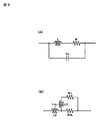
- Cited Document 4 discloses an equivalent circuit and a circuit simulator representing a motor coil. When a basic equivalent circuit of the inductor is shown, as shown in FIG.
- a parasitic capacitance Cp is connected in parallel to a series circuit in which an inductance L and a resistor R representing a loss including a skin effect of a conductor are connected in series. It becomes a connected circuit.
- Each element depends on the frequency.
- circuit analysis such as SPICE is performed using such an equivalent circuit, a large error occurs due to the presence of frequency characteristics of each element, and the actual performance of the designed circuit is the performance of the designed circuit. Is far from the target value.
- Non-Patent Document 2 discloses a ladder circuit that takes into consideration the skin effect of a metal and the proximity effect of an electromagnetic wave.
- FIG. 6B shows the circuit configuration. In order to capture the frequency characteristics of the frequency-dependent equivalent inductance L and conductor resistance R in the basic equivalent circuit, the inductance L0 with respect to DC and the DC resistance of the conductor are shown.
- a series connection circuit of an inductance L1 and a resistance R1 taking into account the metal skin effect is connected in parallel to the DC resistance Rdc of the conductor.
- a mutual inductance Lm is added between the inductances L0 and L1.
- Each circuit element does not depend on the frequency.
- the characteristics obtained by using the equivalent circuit of the background art as described above do not necessarily reflect the characteristics of the actual multilayer chip inductor well, and when performing circuit design using a circuit simulator, etc. Precise characteristic prediction in the frequency band is difficult.
- the effect of each parasitic component is increased on the high frequency side, the multilayer chip inductance characteristics are complicated, and cannot always be expressed well.
- the present invention focuses on the above points, and is an equivalent circuit of a multilayer chip inductor that can satisfactorily suppress the occurrence of errors due to frequency fluctuations between target performance and actual circuit performance in circuit design using a circuit simulator. It is an object of the present invention to provide a model circuit constant analysis method and a circuit simulation method.
- a circuit constant analysis method for an equivalent circuit model of a multilayer chip inductor includes a rectangular parallelepiped dielectric chip, a chip built in the chip, and an end portion that is drawn to the surface of the chip.
- a circuit constant analysis method for an equivalent circuit model of a multilayer chip inductor having an inner conductor and an outer electrode formed on the surface of the chip so as to be conductively connected to an end of the inner conductor,
- a mutual inductance Lm between the inductance L0 for direct current and the inductance L1 for considering the electromagnetic proximity effect is provided.
- a first parallel circuit is configured by connecting in parallel, and the inductance L0 is connected in series to one end of the first parallel circuit.
- a DC resistance Rdc1 of the inner conductor is connected in series to the other end of the first parallel circuit to constitute a second series circuit, and the parasitic capacitance Cp and the loss of the dielectric constituting the chip are reduced.
- a third series circuit connected in series with the resistor Rp shown is connected in parallel to the second series circuit to form a second parallel circuit, and one end of the second parallel circuit is connected to one end of the external electrode.
- An impedance value of an equivalent circuit model of a multilayer chip inductor in which a parasitic inductance Ls is connected in series and a DC resistance Rdc2 of an external electrode is connected in series to the other end of the second parallel circuit, and the multilayer chip
- the circuit constant value included in the equivalent circuit model is determined so that the typical value of the relative error between the actually measured value of the impedance of the inductor is small.
- a fourth series circuit in which an inductance L2 and a resistance R2 for considering the thickness of the internal conductor are connected in series is added to the first parallel circuit of the equivalent circuit model. It is characterized by being connected in parallel.
- the circuit constant value of the equivalent circuit is determined so that the typical value of the relative error is 10% or less.
- the circuit simulation method of the present invention is a circuit simulation method for simulating the characteristics of a circuit including a multilayer chip inductor, using an equivalent circuit model of the multilayer chip inductor whose circuit constant is determined by the circuit constant analysis method. It is characterized by simulating the characteristics of a circuit including a chip inductor.
- an equivalent circuit constant is extracted based on an equivalent circuit model that takes into account dielectric loss in a multilayer chip inductor, inductance and resistance of an external electrode, skin effect and electromagnetic proximity effect of an internal conductor, and thickness of the internal conductor.
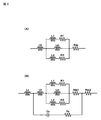
- FIG. 1 is a circuit diagram showing an equivalent circuit of Embodiment 1 of the present invention.
- FIG. 2 is a circuit diagram showing an equivalent circuit of Embodiment 2 of the present invention.
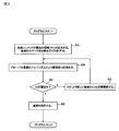
- FIG. 3 is a flowchart showing an example of a technique for specifically obtaining the circuit constant in the equivalent circuit.
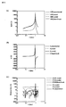
- FIG. 4 is a graph showing the characteristics based on the equivalent circuit of the embodiment compared with the background art and actual measurement values.
- FIG. 5 is a block diagram showing an example of a simulation apparatus to which the present invention is applied.
- FIG. 6 is a circuit diagram showing an example of a conventional equivalent circuit.
- the DC resistance is not a DC resistance Rdc of the originally defined conductor, but a parallel circuit of Rdc and R1. Therefore, in the present invention, as shown in FIG. 1A, a series circuit of an inductance L1 and a resistance R1 considering the skin effect of the conductor is short-circuited with respect to the direct current, and then the inductance L0 with respect to the direct current and the direct current resistance of the conductor Connect in series with Rdc.
- the inductance Ls of the external electrode is connected in series to the inductance L0, and the DC resistance Rdc2 of the external electrode is connected in series to the DC resistance Rdc1 of the internal conductor.
- a series circuit in which a parasitic capacitance Cp of a dielectric constituting the chip of the multilayer chip inductor and a resistor Rp representing a loss of the dielectric are connected in series is connected in parallel inside the equivalent elements Ls and Rdc2 of the external electrodes.
- the SPICE file of the equivalent circuit of FIG. 1C is as follows, for example. . subckt HK1 1 2 Ls 1 3 Lval1 L0 3 4 Lval2 Lm 4 5 Lval3 L1 4 7 Lval4 R1 7 5 Rval1 Cp 3 8 Cval1 Rp 8 6 Rval2 Rdc1 5 6 Rval3 Rdc2 6 2 Rval4 . ends If necessary, a part name or copyright notice is added as a comment.
- specific circuit constant values are described in Lval1, Lval2,. For example, when the value of Ls is 0.58 nH, Ls 1 3 0.58n Is described. Specific examples will be described later.
- the SPICE model program file described in Fortran is as follows.
- the above-mentioned SPICE file can be directly read into the SPICE simulator, but the following program files need to be compiled. Also in this case, a part name and a copyright notice are added as comments as necessary.
- the equivalent circuit shown in FIG. 2A is obtained in consideration of the thickness of the metal layer constituting the internal conductor in the multilayer chip inductor. That is, the skin effect on the side surface of the metal layer is represented by a series circuit of an inductance L2 and a resistance R2, and this is expressed in a series circuit and decoupling form of an inductance L1 and a resistance R1 in consideration of the skin effect of both upper and lower main surfaces of the metal layer. Each of the expressed inductances Lm is connected in parallel.
- the parasitic inductance Ls of the external electrode is connected in series to the inductance L0
- the DC resistance Rdc2 of the external electrode is connected in series to the DC resistance Rdc1 of the internal conductor.
- a series circuit in which a parasitic capacitance Cp of a dielectric constituting the chip and a resistor Rp representing a loss of the dielectric material are connected in series is connected in parallel inside the equivalent elements Ls and Rdc2 of the external electrodes.
- the SPICE file of the equivalent circuit shown in FIG. 2B as described above is, for example, as follows. .
- Z_test (f n ) ESR_test (f n ) + jX_test (f n ) Is the measured value of the impedance at the frequency f n of the specific component of interest.
- Z_circuit (V, f n ) ESR_circuit (V, f n ) + jX_circuit (V, f n ) Is the circuit impedance at the frequency f n of the SPICE model of the component.
- An optimized mathematical model for extracting circuit constants is expressed by the following equation (1) or equation (2).
- the target functions represented by these mathematical expressions are defined by defining a relative error between the measured value of the impedance of the corresponding element and the impedance value in the SPICE model, and minimizing the relative error.
- Equation 1 represents the total error of all bands.
- Equation 2 represents the maximum value of the error between the real part and the imaginary part of the impedance for each frequency.
- FIG. 3 shows a flowchart of the procedure by the global optimization algorithm. As shown in the figure, first, the first region [V A , V B ] of the circuit element is determined (step SA). The first region [V A , V B ] is made as large as possible so that the optimum solution to be found is included as much as possible. Then, an optimal solution is obtained at a time by the global optimization algorithm. Simulation time can be greatly reduced. Next, an optimal solution V 0 is obtained by a global optimization algorithm (step SB).
- Step SC an error in circuit impedance is obtained, and it is determined whether or not the optimum solution V 0 is appropriate.
- the error between the circuit impedance of the SPICE model and the measured value of the component is too large and the optimum solution V 0 is not appropriate (N in step SC)
- a new region [V A is obtained by the optimum solution V 0 . , V B ] is reconstructed (step SD), and the optimum solution V 0 is obtained again by the global optimization algorithm (step SB).
- the error between the circuit impedance by the SPICE model and the actual measurement value of the component represents the accuracy of the SPICE model.
- Equation 3 represents the relative error of ESR
- Equation 4 represents the relative error of reactance.
- a typical value of noise included in the raw data of the actual measurement value for the multilayer chip inductor is 10 %.
- the circuit constants of the equivalent circuit of the embodiment were obtained by the method as described above, and this was input to the SPICE simulator for simulation, and the equivalent circuit model of the present invention was verified. Next, numerical examples obtained as described above will be specifically described.
- FIG. 4A is a graph showing the frequency change of ESR (resistance component). As shown in the figure, the first and second embodiments are very close to the actually measured values, but the basic circuit graph is far away. Moreover, when Example 1 and Example 2 are compared, it turns out that Example 2 has very high precision. Similar results are obtained for the frequency change of X (reactance) in FIG. FIG. 4C shows the relative error of ESR and X with respect to the actual measurement values of Examples 1 and 2 and the basic circuit. From these graphs, it can be seen that the equivalent circuits of Example 1 and Example 2 have very few errors compared to the basic circuit. Similar comparisons were made for other multilayer chip inductors. However, in the SPICE models of all products, simulation results that were very consistent with the actual measurement values were obtained, and the accuracy of Example 2 was further improved than that of Example 1. Confirmed to do.
- ESR resistance component
- the simulation apparatus 100 is configured by a general computer system, and includes an arithmetic processing unit 110 mainly configured by a CPU, an input unit 122 such as a keyboard, an output unit 124 such as a liquid crystal display, and a program memory. 130 and the data memory 140 are connected.
- the program memory 130 stores a simulation program such as a SPICE simulator 132.
- the data memory 140 stores not only the above-described SPICE file of the multilayer chip inductor but also SPICE files 142 of various electronic components such as other capacitors and registers.
- the arithmetic processing unit 110 reads the SPICE file of the element included in the circuit to be simulated from the data memory 140, incorporates it into the SPICE simulator 132, and performs arithmetic processing for simulation such as circuit characteristics. Is done. At this time, a highly accurate simulation result can be obtained by using the SPICE file of the equivalent circuit of Example 1 or Example 2 described above for the multilayer chip inductor. As described above, according to the embodiment of the present invention, the following effects can be obtained. (1) Electronic component manufacturers and their trading companies provide customers with the above-mentioned SPICE models of multilayer chip inductors, or make them public on the company's home page to provide convenience in circuit design to customers who adopt their products. Can be planned.
- the electronic component manufacturer or its agent trading company can publish the SPICE model of the multilayer chip inductor component in a SPICE file or program, install it in a commercially available SPICE simulator, or make it available on the company's home page so that customers can download it. By doing so, it is possible to expand the sales channel of its products.
- this invention is not limited to the Example mentioned above, A various change can be added in the range which does not deviate from the summary of this invention. For example, the following are also included.
- the numerical values of the equivalent circuit constants shown in the above embodiment are merely examples, and are different depending on the parts.
- the above embodiment is an example in which the present invention is applied to a SPICE simulator, but it does not preclude application to other various simulators.
- a resistance element having a very small resistance value and an inductance element having a very small inductance value can be changed to a short circuit.
- a resistance element having an extremely large resistance value and an inductance element having an extremely large inductance value can be changed to an open circuit.
- the multilayer chip inductor since the characteristics of the multilayer chip inductor are accurately represented, it is suitable for various circuit simulations including the multilayer chip inductor.
Landscapes
- Engineering & Computer Science (AREA)
- Computer Hardware Design (AREA)
- Physics & Mathematics (AREA)
- Theoretical Computer Science (AREA)
- Microelectronics & Electronic Packaging (AREA)
- Evolutionary Computation (AREA)
- Geometry (AREA)
- General Engineering & Computer Science (AREA)
- General Physics & Mathematics (AREA)
- Design And Manufacture Of Integrated Circuits (AREA)
- Semiconductor Integrated Circuits (AREA)
Abstract
回路シミュレータを用いた回路設計と実際の回路性能との誤差の発生を良好に抑制する。 内部導体の表皮効果を考慮するインダクタンスL1とレジスタンスR1の直列回路に、直流に対するインダクタンスL0とインダクタンスL1との間の相互インダクタンスLmを並列接続し、これにインダクタンスL0と内部導体の直流抵抗Rdc1とを直列に接続する。次に、外部電極の寄生インダクタンスLsを等価インダクタンスL0に直列に接続するとともに、外部電極の直流抵抗Rdc2を内部導体の直流抵抗Rdc1に直列に接続する。また、寄生キャパシタンスCpと、チップを構成する誘電体の損失を表す抵抗Rpとを直列に接続した直列回路を、外部電極の等価素子Ls,Rdc2の内側に並列に接続して構成された等価回路モデルを用いる。
Description
本発明は、積層チップインダクタの等価回路モデルの回路定数解析方法及び回路シミュレーション方法に関し、特に高周波用の直方体状の誘電体チップと、該チップに内蔵されるとともに端部がそれぞれ前記チップの表面に引き出された内部導体と、前記内部導体の端部に導電接続するように前記チップの表面に形成された外部電極と、を有する積層チップインダクタを含む回路の特性シミュレーションに好適な積層チップインダクタの等価回路モデルの回路定数解析方法及び回路シミュレーション方法の改良に関する。
インダクタを含む回路の特性シミュレーションに関する背景技術としては、例えば、下記特許文献1~4に開示されたものがある。特許文献1には、フェライト材を用いたインダクタンス素子の特性を良好に表すことができる精度の高い等価回路及びその解析手法等が開示されている。特許文献2には、半導体基板上に形成され周波数依存性が少ないインダクタンス素子を表す等価回路及びそのシミュレーション方法が開示されている。引用文献3には、誘電体基板の上面に形成された平面型インダクタンス素子の評価方法が開示されている。引用文献4には、モータコイルを表す等価回路及び回路シミュレータが開示されている。
インダクタの基本的な等価回路を示すと、図6(A)に示すように、インダクタンスLと導体の表皮効果を含む損失を表す抵抗Rとを直列に接続した直列回路に、寄生キャパシタンスCpを並列接続した回路となる。各素子は、いずれも周波数に依存する。このような等価回路を使用してSPICEなどの回路シミュレータで回路解析を行なうと、各素子の周波数特性の存在に起因して大きな誤差が発生し、設計した回路の実際の性能が設計回路の性能の目標値から大きく外れてしまう。
かかる問題点を改善するものとして、下記非特許文献1記載の回路モデリング手法がある。これは、回路素子のモデリングを行なう際に分数多項式を2次ごとに分解し、直列共振回路の並列接続や並列共振回路の直列接続で合成するようにしたものである。しかし、このような一般分数多項式による回路合成の手法で高い精度を達成するためには、多項式の次数を上げなければならず、回路構成が相当複雑になってしまう。
これに対し、下記非特許文献2には、金属の表皮効果(skin effect)と電磁の近接効果(proximity effect)を考慮したラダー回路が開示されている。図6(B)にはその回路構成が示されており、前記基本等価回路に、周波数に依存する等価インダクタンスLと導体の抵抗Rの周波数特性を捉えるため、直流に対するインダクタンスL0と導体の直流抵抗Rdcを直列接続した回路において、金属表皮効果を考慮するインダクタンスL1とレジスタンスR1の直列接続回路を導体の直流抵抗Rdcに並列に接続している。また、電磁近接効果を考慮するため、前記インダクタンスL0,L1間に相互インダクタンスLmを加えている。各回路素子は、いずれも周波数に依存しない。
しかしながら、以上のような背景技術の等価回路を使用して得た特性は、実際の積層チップインダクタの特性を必ずしも良好に反映しておらず、回路シミュレータによる回路設計等を行なう際において、所望の周波数帯域における精度の良い特性予測が難しい。特に、高周波側で各寄生成分の作用が大きくなり、積層チップインダクタンス特性が複雑化し、必ずしも良好に表現することができない。
特開平11−312187号公報
特開2004−235279号公報公報
特開2000−28662号公報
特開2007−122574号公報
河野通孝,加藤利次,井上馨「最小自乗法による集中定数等価回路のパラメータ抽出法」,The SCIENCE and ENGINEERING REVIEW of DOSHISHA UNIVERSITY,Vol.45,No.2 pp.1−14,July 2004
Yu Cao;Groves,R.A.;Xuejue Huang;Zamdmer,N.D.;Plouchart,J.−O.;Wachnik,R.A.;Tsu−Jae King;Chenming Hu,″Frequency−independent equivalent−circuit model for on−chip spiral inductors″,IEEE Journal of Solid−State Circuits,Volume 38,Issue 3,Mar 2003 Page(s):419−426
インダクタの基本的な等価回路を示すと、図6(A)に示すように、インダクタンスLと導体の表皮効果を含む損失を表す抵抗Rとを直列に接続した直列回路に、寄生キャパシタンスCpを並列接続した回路となる。各素子は、いずれも周波数に依存する。このような等価回路を使用してSPICEなどの回路シミュレータで回路解析を行なうと、各素子の周波数特性の存在に起因して大きな誤差が発生し、設計した回路の実際の性能が設計回路の性能の目標値から大きく外れてしまう。
かかる問題点を改善するものとして、下記非特許文献1記載の回路モデリング手法がある。これは、回路素子のモデリングを行なう際に分数多項式を2次ごとに分解し、直列共振回路の並列接続や並列共振回路の直列接続で合成するようにしたものである。しかし、このような一般分数多項式による回路合成の手法で高い精度を達成するためには、多項式の次数を上げなければならず、回路構成が相当複雑になってしまう。
これに対し、下記非特許文献2には、金属の表皮効果(skin effect)と電磁の近接効果(proximity effect)を考慮したラダー回路が開示されている。図6(B)にはその回路構成が示されており、前記基本等価回路に、周波数に依存する等価インダクタンスLと導体の抵抗Rの周波数特性を捉えるため、直流に対するインダクタンスL0と導体の直流抵抗Rdcを直列接続した回路において、金属表皮効果を考慮するインダクタンスL1とレジスタンスR1の直列接続回路を導体の直流抵抗Rdcに並列に接続している。また、電磁近接効果を考慮するため、前記インダクタンスL0,L1間に相互インダクタンスLmを加えている。各回路素子は、いずれも周波数に依存しない。
しかしながら、以上のような背景技術の等価回路を使用して得た特性は、実際の積層チップインダクタの特性を必ずしも良好に反映しておらず、回路シミュレータによる回路設計等を行なう際において、所望の周波数帯域における精度の良い特性予測が難しい。特に、高周波側で各寄生成分の作用が大きくなり、積層チップインダクタンス特性が複雑化し、必ずしも良好に表現することができない。
本発明は以上の点に着目したもので、回路シミュレータを用いた回路設計における目標性能と実際の回路性能との周波数変動に伴う誤差の発生を良好に抑制することができる積層チップインダクタの等価回路モデルの回路定数解析方法及び回路シミュレーション方法を提供することを、その目的とする。
前記目的を達成するため、本発明の積層チップインダクタの等価回路モデルの回路定数解析方法は、直方体状の誘電体チップと、該チップに内蔵されるとともに端部がそれぞれ前記チップの表面に引き出された内部導体と、前記内部導体の端部に導電接続するように前記チップの表面に形成された外部電極と、を有する積層チップインダクタの等価回路モデルの回路定数解析方法であって、内部導体の表皮効果を考慮するためのインダクタンスL1とレジスタンスR1とが直列接続された第1の直列回路に、電磁近接効果を考慮するための、直流に対するインダクタンスL0と前記インダクタンスL1との間の相互インダクタンスLmを並列に接続して第1の並列回路を構成し、該第1の並列回路の一端に、前記インダクタンスL0を直列接続するとともに、前記第1の並列回路の他端に、前記内部導体の直流抵抗Rdc1を直列接続して、第2の直列回路を構成し、寄生キャパシタンスCpと前記チップを構成する誘電体の損失を示す抵抗Rpとが直列接続された第3の直列回路を、前記第2の直列回路に並列接続して、第2の並列回路を構成し、該第2の並列回路の一端に、外部電極の寄生インダクタンスLsを直列接続するとともに、前記第2の並列回路の他端に、外部電極の直流抵抗Rdc2を直列接続して構成した、積層チップインダクタの等価回路モデルのインピーダンスの値と、前記積層チップインダクタのインピーダンスの実測値と、の相対誤差のティピカル値が小さくなるように、前記等価回路モデルに含まれている回路定数の数値を決定することを特徴とする。
主要な形態の一つは、内部導体の厚みを考慮するためのインダクタンスL2とレジスタンスR2とが直列に接続された第4の直列回路を、前記等価回路モデルの前記第1の並列回路に、更に並列に接続したことを特徴とする。
また、他の形態の一つは、前記相対誤差のティピカル値が10%以下となるように等価回路の回路定数の数値を決定することを特徴とする。
本発明の回路シミュレーション方法は、積層チップインダクタを含む回路の特性シミュレーションを行う回路シミュレーション方法において、前記回路定数解析方法によって回路定数が決定された積層チップインダクタの等価回路モデルを利用して、当該積層チップインダクタを含む回路の特性のシミュレーションを行なうことを特徴とする。
主要な形態の一つは、内部導体の厚みを考慮するためのインダクタンスL2とレジスタンスR2とが直列に接続された第4の直列回路を、前記等価回路モデルの前記第1の並列回路に、更に並列に接続したことを特徴とする。
また、他の形態の一つは、前記相対誤差のティピカル値が10%以下となるように等価回路の回路定数の数値を決定することを特徴とする。
本発明の回路シミュレーション方法は、積層チップインダクタを含む回路の特性シミュレーションを行う回路シミュレーション方法において、前記回路定数解析方法によって回路定数が決定された積層チップインダクタの等価回路モデルを利用して、当該積層チップインダクタを含む回路の特性のシミュレーションを行なうことを特徴とする。
本発明によれば、積層チップインダクタにおける誘電体損失,外部電極のインダクタンス及びレジスタンス,内部導体の表皮効果と電磁近接効果、内部導体の厚みを考慮した等価回路モデルに基づいて等価回路定数を抽出することで、回路シミュレータを用いた回路設計と回路の実際の性能との誤差の発生が良好に抑制されるようになる。本発明の前記及び他の目的,特徴,利点は、以下の詳細な説明及び添付図面から明らかにする。
図1は本発明の実施例1の等価回路を示す回路図である。
図2は本発明の実施例2の等価回路を示す回路図である。
図3は前記等価回路における回路定数を具体的に求めるための手法の一例を示すフローチャートである。
図4は前記実施例の等価回路に基づく特性を背景技術及び実測値と比較して示すグラフである。
図5は本発明が適用されるシミュレーション装置の一例を示すブロック図である。
図6は従来の等価回路の一例を示す回路図である。
図2は本発明の実施例2の等価回路を示す回路図である。
図3は前記等価回路における回路定数を具体的に求めるための手法の一例を示すフローチャートである。
図4は前記実施例の等価回路に基づく特性を背景技術及び実測値と比較して示すグラフである。
図5は本発明が適用されるシミュレーション装置の一例を示すブロック図である。
図6は従来の等価回路の一例を示す回路図である。
以下、本発明を実施するための最良の形態を、実施例に基づいて詳細に説明する。
最初に、本発明の理解を容易にするため、図1を参照しながら、上述したラダー回路から本願発明の等価回路に至る経過を説明する。図6(B)に示したCao氏らのラダー回路は、直流抵抗が、本来定義された導体の直流抵抗Rdcではなく、RdcとR1との並列回路となってしまっている。そこで、本発明では、図1(A)に示すように、導体の表皮効果を考慮するインダクタンスL1とレジスタンスR1の直列回路を直流に対してショートしてから、直流に対するインダクタンスL0と導体の直流抵抗Rdcに直列接続する。
次に、この図1(A)の改良したラダー回路に含まれているインダクタンスL0,L1間の相互インダクタンスLmをデカップリング形式で表すと、同図(B)に示すようになる。すなわち、R1・L1の直列回路に相互インダクタンスLmが並列接続されており、この並列回路に、直流に対するインダクタンスL0と導体の直流抵抗Rdcとを直列に接続した構成となる。
次に、誘電体損失と、外部電極のインダクタンス及びレジスタンスを同時に考慮し、図1(C)に示す本実施例の等価回路を得る。すなわち、外部電極のインダクタンスLsを前記インダクタンスL0に直列に接続するとともに、外部電極の直流抵抗Rdc2を内部導体の直流抵抗Rdc1に直列に接続する。また、積層チップインダクタのチップを構成する誘電体の寄生キャパシタンスCpと、誘電体の損失を表す抵抗Rpとを直列に接続した直列回路を、外部電極の等価素子Ls,Rdc2の内側に並列に接続する。
次に、以上のような本実施例における積層チップインダクタの等価回路(SPICEモデル)を使用してシミュレーションを行なう場合について説明する。シミュレータとして、例えばSPICEシミュレータを使用する場合、前記図1(C)の等価回路のSPICEファイルは、例えば下記の通りになる。
.subckt HK1 1 2
Ls 1 3 Lval1
L0 3 4 Lval2
Lm 4 5 Lval3
L1 4 7 Lval4
R1 7 5 Rval1
Cp 3 8 Cval1
Rp 8 6 Rval2
Rdc1 5 6 Rval3
Rdc2 6 2 Rval4
.ends
なお、必要に応じて、部品名や著作権表示がコメントとして付加される。また、上記ファイル中、Lval1,Lval2,・・・には、具体的な回路定数の数値が記述される。例えば、Lsの値が0.58nHのときは、
Ls 1 3 0.58n
と記述されるという具合である。具体例は後述する。
次に、Fortranで記述したSPICEモデルのプログラムファイルは、下記の通りになる。上述したSPICEファイルは、そのままSPICEシミュレータに読み込むことができるが、以下のプログラムファイルは、コンパイルする必要がある。この場合も、必要に応じて、部品名や著作権表示がコメントとして付加される。
Complex Function ZHK1(Ls,L0,Lm,L1,R1,Cp,Rp,Rdc1,Rdc2,Freq)
Complex AIM,ZLs,ZL0,ZLm,ZL1,ZCp,Z1,Z2,Z3
data PI/3.1415926/,AIM/(0.0,1.0)
ZLs=AIM*2.0*PI*Freq*Ls
ZL0=AIM*2.0*PI*Freq*L0
ZLm=AIM*2.0*PI*Freq*Lm
ZL1=AIM*2.0*PI*Freq*L1
ZCp=1./(AIM*2.0*PI*Freq*Cp)
Z1=R1+ZL1
Z2=ZL0+1./(1./ZLm+1./Z1)+Rdc1
Z3=1./(1./Z2+1./(ZCp+Rp))
ZHK1=ZLs+Z3+Rdc2
Return
End
次に、この図1(A)の改良したラダー回路に含まれているインダクタンスL0,L1間の相互インダクタンスLmをデカップリング形式で表すと、同図(B)に示すようになる。すなわち、R1・L1の直列回路に相互インダクタンスLmが並列接続されており、この並列回路に、直流に対するインダクタンスL0と導体の直流抵抗Rdcとを直列に接続した構成となる。
次に、誘電体損失と、外部電極のインダクタンス及びレジスタンスを同時に考慮し、図1(C)に示す本実施例の等価回路を得る。すなわち、外部電極のインダクタンスLsを前記インダクタンスL0に直列に接続するとともに、外部電極の直流抵抗Rdc2を内部導体の直流抵抗Rdc1に直列に接続する。また、積層チップインダクタのチップを構成する誘電体の寄生キャパシタンスCpと、誘電体の損失を表す抵抗Rpとを直列に接続した直列回路を、外部電極の等価素子Ls,Rdc2の内側に並列に接続する。
次に、以上のような本実施例における積層チップインダクタの等価回路(SPICEモデル)を使用してシミュレーションを行なう場合について説明する。シミュレータとして、例えばSPICEシミュレータを使用する場合、前記図1(C)の等価回路のSPICEファイルは、例えば下記の通りになる。
.subckt HK1 1 2
Ls 1 3 Lval1
L0 3 4 Lval2
Lm 4 5 Lval3
L1 4 7 Lval4
R1 7 5 Rval1
Cp 3 8 Cval1
Rp 8 6 Rval2
Rdc1 5 6 Rval3
Rdc2 6 2 Rval4
.ends
なお、必要に応じて、部品名や著作権表示がコメントとして付加される。また、上記ファイル中、Lval1,Lval2,・・・には、具体的な回路定数の数値が記述される。例えば、Lsの値が0.58nHのときは、
Ls 1 3 0.58n
と記述されるという具合である。具体例は後述する。
次に、Fortranで記述したSPICEモデルのプログラムファイルは、下記の通りになる。上述したSPICEファイルは、そのままSPICEシミュレータに読み込むことができるが、以下のプログラムファイルは、コンパイルする必要がある。この場合も、必要に応じて、部品名や著作権表示がコメントとして付加される。
Complex Function ZHK1(Ls,L0,Lm,L1,R1,Cp,Rp,Rdc1,Rdc2,Freq)
Complex AIM,ZLs,ZL0,ZLm,ZL1,ZCp,Z1,Z2,Z3
data PI/3.1415926/,AIM/(0.0,1.0)
ZLs=AIM*2.0*PI*Freq*Ls
ZL0=AIM*2.0*PI*Freq*L0
ZLm=AIM*2.0*PI*Freq*Lm
ZL1=AIM*2.0*PI*Freq*L1
ZCp=1./(AIM*2.0*PI*Freq*Cp)
Z1=R1+ZL1
Z2=ZL0+1./(1./ZLm+1./Z1)+Rdc1
Z3=1./(1./Z2+1./(ZCp+Rp))
ZHK1=ZLs+Z3+Rdc2
Return
End
次に、図2を参照しながら、本発明の実施例2について説明する。前記図1(B)に示したデカップリング形式のラダー回路において、積層チップインダクタにおいて内部導体を構成する金属層の厚みを考慮すると、図2(A)に示すような等価回路となる。すなわち、金属層の側面の表皮効果をインダクタンスL2とレジスタンスR2の直列回路で表し、これを、金属層の上下両主面の表皮効果を考慮したインダクタンスL1とレジスタンスR1の直列回路及びデカップリング形式で表現したインダクタンスLmと、それぞれ並列に接続する。
次に、前記実施例と同様にして、誘電体損失と、外部電極の寄生インダクタンス及びレジスタンスを同時に考慮し、図2(B)に示す本実施例の等価回路を得る。すなわち、外部電極の寄生インダクタンスLsを前記インダクタンスL0に直列に接続するとともに、外部電極の直流抵抗Rdc2を内部導体の直流抵抗Rdc1に直列に接続する。また、チップを構成する誘電体の寄生キャパシタンスCpと、誘電体材料の損失を表す抵抗Rpとを直列に接続した直列回路を、外部電極の等価素子Ls,Rdc2の内側に並列に接続する。
以上のような図2(B)に示す等価回路のSPICEファイルは、例えば下記の通りになる。
.subckt HK2 1 2
Ls 1 3 Lval1
L0 3 4 Lval2
Lm 4 5 Lval3
L1 4 7 Lval4
R1 7 5 RVal1
L2 4 8 Lval5
R2 8 5 Rval2
Cp 3 9 Cval1
Rp 9 6 Rval3
Rdc1 5 6 Rval4
Rdc2 6 2 Rval5
.ends
また、Fortranによる前記SPICEモデルのプログラムファイルは、下記の通りになる。
Complex Function ZHK2(Ls,L0,Lm,L1,R1,L2,R2,
1 Cp,Rp,Rdc1,Rdc2,Freq)
Complex AIM,ZLs,ZL0,ZLm,ZL1,Zl2,ZCp,Z1,Z2,Z3
data PI/3.1415926/,AIM/(0.0,1.0)
ZLs=AIM*2.0*PI*Freq*Ls
ZL0=AIM*2.0*PI*Freq*L0
ZLm=AIM*2.0*PI*Freq*Lm
ZL1=AIM*2.0*PI*Freq*L1
ZL2=AIM*2.0*PI*Freq*L2
ZCp=1./(AIM*2.0*PI*Freq*Cp)
Z1=1./(1./ZLm+1./(R1+ZL1)+1./(R2LZL2))
Z2=ZL0+Z1+Rdc1
Z3=1./(1./Z2+1./(ZCp+Rp))
ZHK2=ZLs+Z3+Rdc2
Return
End
<具体例>
次に、図3~図4を参照しながら、前記実施例の具体的な数値例及びシミュレーション例を説明する。上述した実施例の等価回路モデルを利用してシミュレーションを行なうためには、各等価回路に含まれている回路定数を具体的に決定する必要がある。例えば、ABC社製の型番「○○○」の積層チップインダクタを使用するときは、当該部品における前記回路定数の値を具体的に決定しなければならない。そのための手法としては、ニュートン法など、各種の手法が知られているが、以下、一例として、グローバル最適化アルゴリズムによる方法を説明する。まず、
Z_test(fn)=ESR_test(fn)+jX_test(fn)
を、対象となる特定の部品の周波数fnにおけるインピーダンスの実測値とする。また、
Z_circuit(V,fn)=ESR_circuit(V,fn)+jX_circuit(V,fn)
を、当該部品のSPICEモデルの周波数fnにおける回路インピーダンスとする。なお、これらの式中のV={V1,V2,…,Vm},Vi(i=1,2,…,m)は、SPICEモデルの回路素子である。
回路定数を抽出する最適化数学モデルは、次の数1式,あるいは数2式で示される。これらの数式で表される目標関数は、該当する素子のインピーダンスの実測値と、SPICEモデルにおけるインピーダンス値との相対誤差を定義し、その相対誤差を最小化して表したものである。数1式は、全帯域の誤差の合計を表したものである。数2式は、周波数ごとのインピーダンスの実数部と虚数部の誤差の最大値を表したものである。

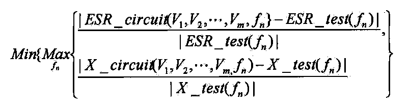
図3には、前記グローバル最適化アルゴリズムによる手順がフローチャートとして示されている。同図に示すように、まず、回路素子の最初の領域[VA,VB]を決める(ステップSA)。求める最適解がなるべく含まれるように最初の領域[VA,VB]を出来るだけ大きくする。そうすると、グローバル最適化アルゴリズムにより一回で最適解が求められる。シミュレーション時間は大幅短縮できる。
次に、グローバル最適化アルゴリズムにより最適解V0を求める(ステップSB)。そして、前記数1式及び数2式を利用して、回路インピーダンスの誤差を求め、最適解V0が適切かどうか判断する(ステップSC)。その結果、もしSPICEモデルの回路インピーダンスと部品の実測値との誤差が大き過ぎて、前記最適解V0が適切でないと判明したら(ステップSCのN)、最適解V0によって新しい領域[VA,VB]を再構成し(ステップSD)、グローバル最適化アルゴリズムによって最適解V0をもう一度求める(ステップSB)。
SPICEモデルによる回路インピーダンスと部品の実測値との誤差は、SPICEモデルの精度を表す。この回路インピーダンス対実測値の相対誤差は、次の数3式及び数4式で示される。これらのうち、数3式はESRの相対誤差,数4式はリアクタンスの相対誤差を表す。


以上の処理を繰り返し行ない、回路インピーダンス対実測値の相対誤差のティピカル値が例えば10%以下となったら、高精度のSPICEモデルが得られたと判断し(ステップSCのY)、その結果を保存して終了する(ステップSE)。
なお、相対誤差のティピカル値を10%以下にする理由は二つある。第1に、測定器の確度により、測定誤差を生じ、実測値の生データにノイズが含まれており、積層チップインダクタに対して実測値の生データに入っているノイズのティピカル値は、10%程度である。第2に、電子部品毎の特性ばらつきがあり、積層チップインダクタの公差は一般的にJ交差(±5%)と定められているので、10%より大きいと回路精度が低下してしまう。このため、上記相対誤差のティピカル値は10%以下となるようにすることが好ましい。
次に、以上のような手法で実施例の等価回路の回路定数を求め、これをSPICEシミュレータに入力してシミュレーションを行い、本発明の等価回路モデルを検証した。
次に、以上のようにして求めた数値例について具体的に説明する。
(1)本件出願人製の高周波用積層チップインダクタ「HK1005R10(100nH)」の場合(実施例1と実施例2の等価回路の適用範囲はDCもしくは周波数1.942GHz以下)
a,図6(A)に示した基本等価回路をSPICEモデルとして、各素子の回路定数の数値を上記方法で求めたところ、以下のようになった。
L0=100nH,
Rdc=0.894362Ω,
Cp=0.268236pF,
b,次に、図1(C)に示した実施例1の等価回路における各素子の回路定数の数値を求めたところ、以下のようになった。
L0=55.712532nH,
Lm=48.885025nH,
L1=84.4907913nH,
R1=112.035797Ω,
Cp=0.295752853pF,
Rp=3.24151635Ω,
Ls=0.538956523nH,
Rdc1=0.796844184Ω,
Rdc2=0.0975177884Ω。
c,次に、図1(C)に示した実施例2の等価回路における各素子の回路定数の数値を求めたところ、以下のようになった。
L0=66.2275314nH,
Lm=45.4679871nH,
L1=77.8189621nH,
L2=108.25425nH,
R1=39.0474358Ω,
R2=457.259155Ω,
Cp=0.285327792pF,
Rp=2.12735748Ω,
Ls=1.25335538nH,
Rdc1=0.663021684Ω,
Rdc2=0.231340289Ω。
これらに対応するSPICEファイルは、下記の通りとなる。コメント行は省略している。
a,実施例1の場合
.subckt HK1005R10_1 1 2
Ls 1 3 0.538956523n
L0 3 4 55.712532n
Lm 4 5 48.885025n
L1 4 7 84.4907913n
R1 7 5 112.035797
Cp 3 8 0.295752853p
Rp 8 6 3.24151635
Rdc1 5 6 0.796844184
Rdc2 6 2 0.0975177884
.ends
b,実施例2の場合
.subckt HK1005R10_2 1 2
Ls 1 3 1.25335538n
L0 3 4 66.2275314n
Lm 4 5 45.4679871n
L1 4 7 77.8189621n
R1 7 5 39.0474358
L2 4 8 108.25425n
R2 8 5 457.259155
Cp 3 9 0.285327792p
Rp 9 6 2.12735748
Rdc1 5 6 0.663021684
Rdc2 6 2 0.231340289
.ends
プログラミングしたSPICEモデルを呼び出すためのプログラムは、次の通りとなる。コメント行は省略している。
a,実施例1の場合
Complex Function Z_R10_1(Freq)
COMPLEX ZHK1
Ls=0.538956523e−9
L0=55.712532e−9
Lm=48.885025e−9
L1=84.4907913e−9
R1=112.035797
Cp=0.295752853e−12
Rp=3.24151635
Rdc1=0.796844184
Rdc2=0.0975177884
Z_R10_1=ZHK1(Ls,L0,Lm,L1,R1,Cp,Rp,Rdc1,Rdc2,Freq)
Return
End
b,実施例2の場合
Complex Function Z_R10_2(Freq)
COMPLEX ZHK2
Ls=1.25335538e−9
L0=66.2275314e−9
Lm=45.4679871e−9
L1=77.8189621e−9
R1=39.0474358
L2=108.25425e−9
R2=457.259155
Cp=0.285327792e−12
Rp=2.12735748
Rdc1=0.663021684
Rdc2=0.231340289
Z_R10_2=ZHK2(Ls,L0,Lm,L1,R1,L2,R2,
1 Cp,Rp,Rdc1,Rdc2,Freq)
Return
End
次に、以上のようにして得た実施例1及び実施例2の等価回路の回路定数を用いたSPICEシミュレータによる計算結果と、図6(A)に示した基本回路のSPICEシミュレータによる計算結果と、インピーダンスの実測値とを比較する。
図4(A)は、ESR(抵抗分)の周波数変化を示すグラフである。同図に示すように、実施例1及び実施例2は、実測値に極めて近似しているのに対し、基本回路のグラフは大きく離れている。また、実施例1及び実施例2を比較すると、実施例2は極めて高い精度を持っていることが分かる。図4(B)のX(リアクタンス)の周波数変化についても、同様の結果が得られている。図4(C)は、実施例1,2及び基本回路の実測値に対するESR及びXの相対誤差を示したものである。これらのグラフから、実施例1及び実施例2の等価回路は、基本回路と比較して、非常に誤差が少ないことが分かる。他の積層チップインダクタについても、同様の比較を行なったが、全製品のSPICEモデルにおいて、実測値と極めて一致したシミュレーション結果が得られており、実施例2は実施例1よりも精度が更に向上することが確認された。
次に、前記実施例と同様にして、誘電体損失と、外部電極の寄生インダクタンス及びレジスタンスを同時に考慮し、図2(B)に示す本実施例の等価回路を得る。すなわち、外部電極の寄生インダクタンスLsを前記インダクタンスL0に直列に接続するとともに、外部電極の直流抵抗Rdc2を内部導体の直流抵抗Rdc1に直列に接続する。また、チップを構成する誘電体の寄生キャパシタンスCpと、誘電体材料の損失を表す抵抗Rpとを直列に接続した直列回路を、外部電極の等価素子Ls,Rdc2の内側に並列に接続する。
以上のような図2(B)に示す等価回路のSPICEファイルは、例えば下記の通りになる。
.subckt HK2 1 2
Ls 1 3 Lval1
L0 3 4 Lval2
Lm 4 5 Lval3
L1 4 7 Lval4
R1 7 5 RVal1
L2 4 8 Lval5
R2 8 5 Rval2
Cp 3 9 Cval1
Rp 9 6 Rval3
Rdc1 5 6 Rval4
Rdc2 6 2 Rval5
.ends
また、Fortranによる前記SPICEモデルのプログラムファイルは、下記の通りになる。
Complex Function ZHK2(Ls,L0,Lm,L1,R1,L2,R2,
1 Cp,Rp,Rdc1,Rdc2,Freq)
Complex AIM,ZLs,ZL0,ZLm,ZL1,Zl2,ZCp,Z1,Z2,Z3
data PI/3.1415926/,AIM/(0.0,1.0)
ZLs=AIM*2.0*PI*Freq*Ls
ZL0=AIM*2.0*PI*Freq*L0
ZLm=AIM*2.0*PI*Freq*Lm
ZL1=AIM*2.0*PI*Freq*L1
ZL2=AIM*2.0*PI*Freq*L2
ZCp=1./(AIM*2.0*PI*Freq*Cp)
Z1=1./(1./ZLm+1./(R1+ZL1)+1./(R2LZL2))
Z2=ZL0+Z1+Rdc1
Z3=1./(1./Z2+1./(ZCp+Rp))
ZHK2=ZLs+Z3+Rdc2
Return
End
<具体例>
次に、図3~図4を参照しながら、前記実施例の具体的な数値例及びシミュレーション例を説明する。上述した実施例の等価回路モデルを利用してシミュレーションを行なうためには、各等価回路に含まれている回路定数を具体的に決定する必要がある。例えば、ABC社製の型番「○○○」の積層チップインダクタを使用するときは、当該部品における前記回路定数の値を具体的に決定しなければならない。そのための手法としては、ニュートン法など、各種の手法が知られているが、以下、一例として、グローバル最適化アルゴリズムによる方法を説明する。まず、
Z_test(fn)=ESR_test(fn)+jX_test(fn)
を、対象となる特定の部品の周波数fnにおけるインピーダンスの実測値とする。また、
Z_circuit(V,fn)=ESR_circuit(V,fn)+jX_circuit(V,fn)
を、当該部品のSPICEモデルの周波数fnにおける回路インピーダンスとする。なお、これらの式中のV={V1,V2,…,Vm},Vi(i=1,2,…,m)は、SPICEモデルの回路素子である。
回路定数を抽出する最適化数学モデルは、次の数1式,あるいは数2式で示される。これらの数式で表される目標関数は、該当する素子のインピーダンスの実測値と、SPICEモデルにおけるインピーダンス値との相対誤差を定義し、その相対誤差を最小化して表したものである。数1式は、全帯域の誤差の合計を表したものである。数2式は、周波数ごとのインピーダンスの実数部と虚数部の誤差の最大値を表したものである。
次に、グローバル最適化アルゴリズムにより最適解V0を求める(ステップSB)。そして、前記数1式及び数2式を利用して、回路インピーダンスの誤差を求め、最適解V0が適切かどうか判断する(ステップSC)。その結果、もしSPICEモデルの回路インピーダンスと部品の実測値との誤差が大き過ぎて、前記最適解V0が適切でないと判明したら(ステップSCのN)、最適解V0によって新しい領域[VA,VB]を再構成し(ステップSD)、グローバル最適化アルゴリズムによって最適解V0をもう一度求める(ステップSB)。
SPICEモデルによる回路インピーダンスと部品の実測値との誤差は、SPICEモデルの精度を表す。この回路インピーダンス対実測値の相対誤差は、次の数3式及び数4式で示される。これらのうち、数3式はESRの相対誤差,数4式はリアクタンスの相対誤差を表す。
なお、相対誤差のティピカル値を10%以下にする理由は二つある。第1に、測定器の確度により、測定誤差を生じ、実測値の生データにノイズが含まれており、積層チップインダクタに対して実測値の生データに入っているノイズのティピカル値は、10%程度である。第2に、電子部品毎の特性ばらつきがあり、積層チップインダクタの公差は一般的にJ交差(±5%)と定められているので、10%より大きいと回路精度が低下してしまう。このため、上記相対誤差のティピカル値は10%以下となるようにすることが好ましい。
次に、以上のような手法で実施例の等価回路の回路定数を求め、これをSPICEシミュレータに入力してシミュレーションを行い、本発明の等価回路モデルを検証した。
次に、以上のようにして求めた数値例について具体的に説明する。
(1)本件出願人製の高周波用積層チップインダクタ「HK1005R10(100nH)」の場合(実施例1と実施例2の等価回路の適用範囲はDCもしくは周波数1.942GHz以下)
a,図6(A)に示した基本等価回路をSPICEモデルとして、各素子の回路定数の数値を上記方法で求めたところ、以下のようになった。
L0=100nH,
Rdc=0.894362Ω,
Cp=0.268236pF,
b,次に、図1(C)に示した実施例1の等価回路における各素子の回路定数の数値を求めたところ、以下のようになった。
L0=55.712532nH,
Lm=48.885025nH,
L1=84.4907913nH,
R1=112.035797Ω,
Cp=0.295752853pF,
Rp=3.24151635Ω,
Ls=0.538956523nH,
Rdc1=0.796844184Ω,
Rdc2=0.0975177884Ω。
c,次に、図1(C)に示した実施例2の等価回路における各素子の回路定数の数値を求めたところ、以下のようになった。
L0=66.2275314nH,
Lm=45.4679871nH,
L1=77.8189621nH,
L2=108.25425nH,
R1=39.0474358Ω,
R2=457.259155Ω,
Cp=0.285327792pF,
Rp=2.12735748Ω,
Ls=1.25335538nH,
Rdc1=0.663021684Ω,
Rdc2=0.231340289Ω。
これらに対応するSPICEファイルは、下記の通りとなる。コメント行は省略している。
a,実施例1の場合
.subckt HK1005R10_1 1 2
Ls 1 3 0.538956523n
L0 3 4 55.712532n
Lm 4 5 48.885025n
L1 4 7 84.4907913n
R1 7 5 112.035797
Cp 3 8 0.295752853p
Rp 8 6 3.24151635
Rdc1 5 6 0.796844184
Rdc2 6 2 0.0975177884
.ends
b,実施例2の場合
.subckt HK1005R10_2 1 2
Ls 1 3 1.25335538n
L0 3 4 66.2275314n
Lm 4 5 45.4679871n
L1 4 7 77.8189621n
R1 7 5 39.0474358
L2 4 8 108.25425n
R2 8 5 457.259155
Cp 3 9 0.285327792p
Rp 9 6 2.12735748
Rdc1 5 6 0.663021684
Rdc2 6 2 0.231340289
.ends
プログラミングしたSPICEモデルを呼び出すためのプログラムは、次の通りとなる。コメント行は省略している。
a,実施例1の場合
Complex Function Z_R10_1(Freq)
COMPLEX ZHK1
Ls=0.538956523e−9
L0=55.712532e−9
Lm=48.885025e−9
L1=84.4907913e−9
R1=112.035797
Cp=0.295752853e−12
Rp=3.24151635
Rdc1=0.796844184
Rdc2=0.0975177884
Z_R10_1=ZHK1(Ls,L0,Lm,L1,R1,Cp,Rp,Rdc1,Rdc2,Freq)
Return
End
b,実施例2の場合
Complex Function Z_R10_2(Freq)
COMPLEX ZHK2
Ls=1.25335538e−9
L0=66.2275314e−9
Lm=45.4679871e−9
L1=77.8189621e−9
R1=39.0474358
L2=108.25425e−9
R2=457.259155
Cp=0.285327792e−12
Rp=2.12735748
Rdc1=0.663021684
Rdc2=0.231340289
Z_R10_2=ZHK2(Ls,L0,Lm,L1,R1,L2,R2,
1 Cp,Rp,Rdc1,Rdc2,Freq)
Return
End
次に、以上のようにして得た実施例1及び実施例2の等価回路の回路定数を用いたSPICEシミュレータによる計算結果と、図6(A)に示した基本回路のSPICEシミュレータによる計算結果と、インピーダンスの実測値とを比較する。
図4(A)は、ESR(抵抗分)の周波数変化を示すグラフである。同図に示すように、実施例1及び実施例2は、実測値に極めて近似しているのに対し、基本回路のグラフは大きく離れている。また、実施例1及び実施例2を比較すると、実施例2は極めて高い精度を持っていることが分かる。図4(B)のX(リアクタンス)の周波数変化についても、同様の結果が得られている。図4(C)は、実施例1,2及び基本回路の実測値に対するESR及びXの相対誤差を示したものである。これらのグラフから、実施例1及び実施例2の等価回路は、基本回路と比較して、非常に誤差が少ないことが分かる。他の積層チップインダクタについても、同様の比較を行なったが、全製品のSPICEモデルにおいて、実測値と極めて一致したシミュレーション結果が得られており、実施例2は実施例1よりも精度が更に向上することが確認された。
次に、図5を参照しながら、シミュレーション装置の実施例について説明する。本実施例のシミュレーション装置100は、一般的なコンピュータシステムによって構成されており、CPUを中心に構成された演算処理部110に、キーボードなどの入力部122,液晶ディスプレイなどの出力部124,プログラムメモリ130,データメモリ140が接続された構成となっている。プログラムメモリ130には、シミュレーションプログラム,例えばSPICEシミュレータ132が格納されている。データメモリ140には、上述した積層チップインダクタのSPICEファイルのみならず、その他のキャパシタやレジスタなどの各種の電子部品のSPICEファイル142が格納されている。
演算処理部110は、入力部122からの入力指示に基づいて、データメモリ140からシミュレーション対象の回路に含まれる素子のSPICEファイルを読み出し、SPICEシミュレータ132に組み込んで、回路特性などのシミュレーションの演算処理が行われる。このとき、積層チップインダクタについて上述した実施例1あるいは実施例2の等価回路のSPICEファイルを使用することで、非常に精度の高いシミュレーション結果を得ることができる。
以上のように、本発明の実施例によれば、次のような効果が得られる。
(1)電子部品メーカーやその代理商社は、上述した積層チップインダクタのSPICEモデルを顧客に提供し、もしくは会社のホームペイジに公開し、自社製品を採用する顧客に対して回路設計上の便宜を図ることができる。
(2)電子部品メーカーやその代理商社は、前記積層チップインダクタ部品のSPICEモデルをSPICEファイルもしくはプログラミングし、市販のSPICEシミュレータに搭載して、もしくは、顧客がダウンロードできるように会社のホームペイジに公開することで、自社製品の販路の拡大を図ることができる。
(3)電子機器メーカーや電子回路の設計会社は、前記公開されたSPICEモデルを使用することで、電子製品を精度よく設計でき、設計時間が大幅に短縮できる。また、積層チップインダクタ部品の採用の検証,機器故障の解析なども行うことができる。
なお、本発明は、上述した実施例に限定されるものではなく、本発明の要旨に逸脱しない範囲内において種々変更を加え得ることができる。例えば、以下のものも含まれる。
(1)前記実施例で示した等価回路定数の数値は一例であり、部品によって異なる数値となる。
(2)前記実施例は、SPICEシミュレータに対して本発明を適用した例であるが、他の各種のシミュレータに適用することを妨げるものではない。
(3)更に、抵抗値が極めて小さい抵抗素子とインダクタンス値が極めて小さいインダクタンス素子はショート回路に変更することができる。また、抵抗値が極めて大きい抵抗素子とインダクタンス値が極めて大きいインダクタンス素子はオープン回路に変更することができる。
演算処理部110は、入力部122からの入力指示に基づいて、データメモリ140からシミュレーション対象の回路に含まれる素子のSPICEファイルを読み出し、SPICEシミュレータ132に組み込んで、回路特性などのシミュレーションの演算処理が行われる。このとき、積層チップインダクタについて上述した実施例1あるいは実施例2の等価回路のSPICEファイルを使用することで、非常に精度の高いシミュレーション結果を得ることができる。
以上のように、本発明の実施例によれば、次のような効果が得られる。
(1)電子部品メーカーやその代理商社は、上述した積層チップインダクタのSPICEモデルを顧客に提供し、もしくは会社のホームペイジに公開し、自社製品を採用する顧客に対して回路設計上の便宜を図ることができる。
(2)電子部品メーカーやその代理商社は、前記積層チップインダクタ部品のSPICEモデルをSPICEファイルもしくはプログラミングし、市販のSPICEシミュレータに搭載して、もしくは、顧客がダウンロードできるように会社のホームペイジに公開することで、自社製品の販路の拡大を図ることができる。
(3)電子機器メーカーや電子回路の設計会社は、前記公開されたSPICEモデルを使用することで、電子製品を精度よく設計でき、設計時間が大幅に短縮できる。また、積層チップインダクタ部品の採用の検証,機器故障の解析なども行うことができる。
なお、本発明は、上述した実施例に限定されるものではなく、本発明の要旨に逸脱しない範囲内において種々変更を加え得ることができる。例えば、以下のものも含まれる。
(1)前記実施例で示した等価回路定数の数値は一例であり、部品によって異なる数値となる。
(2)前記実施例は、SPICEシミュレータに対して本発明を適用した例であるが、他の各種のシミュレータに適用することを妨げるものではない。
(3)更に、抵抗値が極めて小さい抵抗素子とインダクタンス値が極めて小さいインダクタンス素子はショート回路に変更することができる。また、抵抗値が極めて大きい抵抗素子とインダクタンス値が極めて大きいインダクタンス素子はオープン回路に変更することができる。
本発明によれば、積層チップインダクタの特性が精度よく表されるため、積層チップインダクタを含む各種の回路シミュレーションに好適である。
100 シミュレーション装置
110 演算処理部
122 入力部
124 出力部
130 プログラムメモリ
132 シミュレーションプログラム
140 データメモリ
142 SPICEファイル
110 演算処理部
122 入力部
124 出力部
130 プログラムメモリ
132 シミュレーションプログラム
140 データメモリ
142 SPICEファイル
Claims (4)
- 直方体状の誘電体チップと、該チップに内蔵されるとともに端部がそれぞれ前記チップの表面に引き出された内部導体と、前記内部導体の端部に導電接続するように前記チップの表面に形成された外部電極と、を有する積層チップインダクタの等価回路モデルの回路定数解析方法であって、
前記内部導体の表皮効果を考慮するためのインダクタンスL1とレジスタンスR1とが直列接続された第1の直列回路に、電磁近接効果を考慮するための、直流に対するインダクタンスL0と前記インダクタンスL1との間の相互インダクタンスLmを並列に接続して第1の並列回路を構成し、該第1の並列回路の一端に、前記インダクタンスL0を直列接続するとともに、前記第1の並列回路の他端に、前記内部導体の直流抵抗Rdc1を直列接続して、第2の直列回路を構成し、寄生キャパシタンスCpと前記チップを構成する誘電体の損失を示す抵抗Rpとが直列接続された第3の直列回路を、前記第2の直列回路に並列接続して、第2の並列回路を構成し、該第2の並列回路の一端に、外部電極の寄生インダクタンスLsを直列接続するとともに、前記第2の並列回路の他端に、外部電極の直流抵抗Rdc2を直列接続して構成した、積層チップインダクタの等価回路モデルのインピーダンスの値と、前記積層チップインダクタのインピーダンスの実測値と、の相対誤差のティピカル値が小さくなるように、前記等価回路モデルに含まれている回路定数の数値を決定することを特徴とする積層チップインダクタの等価回路モデルの回路定数解析方法。 - 内部導体の厚みを考慮するためのインダクタンスL2とレジスタンスR2とが直列に接続された第4の直列回路を、前記等価回路モデルの前記第1の並列回路に、更に並列に接続したことを特徴とする請求項1記載の積層チップインダクタの等価回路モデルの回路定数解析方法。
- 前記相対誤差のティピカル値が10%以下となるように等価回路の回路定数の数値を決定することを特徴とする請求項1または2のいずれかに記載の積層体チップインダクタの等価回路モデルの回路定数解析方法。
- 積層チップインダクタを含む回路の特性シミュレーションを行なう回路シミュレーション方法において、
請求項3に記載の回路定数解析方法によって回路定数が決定された積層チップインダクタの等価回路モデルを利用して、当該積層チップインダクタを含む回路の特性のシミュレーションを行なうことを特徴とする回路シミュレーション方法。
Priority Applications (1)
| Application Number | Priority Date | Filing Date | Title |
|---|---|---|---|
| US13/203,689 US20110313749A1 (en) | 2009-03-02 | 2010-02-24 | Circuit constant analysis method and circuit simulation method of equivalent circuit model of multilayer chip inductor |
Applications Claiming Priority (2)
| Application Number | Priority Date | Filing Date | Title |
|---|---|---|---|
| JP2009048674A JP5121757B2 (ja) | 2009-03-02 | 2009-03-02 | 積層チップインダクタの等価回路モデルの回路定数解析方法及び回路シミュレーション方法 |
| JP2009-048674 | 2009-03-02 |
Publications (1)
| Publication Number | Publication Date |
|---|---|
| WO2010101197A1 true WO2010101197A1 (ja) | 2010-09-10 |
Family
ID=42709752
Family Applications (1)
| Application Number | Title | Priority Date | Filing Date |
|---|---|---|---|
| PCT/JP2010/053474 Ceased WO2010101197A1 (ja) | 2009-03-02 | 2010-02-24 | 積層チップインダクタの等価回路モデルの回路定数解析方法及び回路シミュレーション方法 |
Country Status (3)
| Country | Link |
|---|---|
| US (1) | US20110313749A1 (ja) |
| JP (1) | JP5121757B2 (ja) |
| WO (1) | WO2010101197A1 (ja) |
Cited By (1)
| Publication number | Priority date | Publication date | Assignee | Title |
|---|---|---|---|---|
| CN102479263A (zh) * | 2010-11-23 | 2012-05-30 | 中国科学院微电子研究所 | 肖特基变容管的大信号等效电路模型及其提参方法 |
Families Citing this family (11)
| Publication number | Priority date | Publication date | Assignee | Title |
|---|---|---|---|---|
| FR2574972B1 (fr) | 1984-12-18 | 1987-03-27 | Thioulouse Pascal | Dispositif d'affichage a effet memoire comprenant des couches electroluminescente et photoconductrice superposees |
| JP5246785B2 (ja) * | 2009-03-04 | 2013-07-24 | 国立大学法人東京工業大学 | 回路モデル作成装置、回路モデル作成方法、シミュレーション装置、及び、シミュレーション方法 |
| JP5957748B2 (ja) * | 2011-03-11 | 2016-07-27 | 国立大学法人信州大学 | コイルの交流抵抗計算方法 |
| JP5934479B2 (ja) * | 2011-07-25 | 2016-06-15 | 日置電機株式会社 | 等価回路解析装置及び等価回路解析方法 |
| US9281748B2 (en) | 2012-03-02 | 2016-03-08 | Lenovo Enterprise Solutions (Singapore) Pte. Ltd. | Operating a DC-DC converter |
| KR101616037B1 (ko) | 2013-05-14 | 2016-04-27 | 가부시키가이샤 무라타 세이사쿠쇼 | 콘덴서의 시뮬레이션 방법 및 콘덴서의 비선형 등가 회로 모델 |
| WO2014185294A1 (ja) | 2013-05-14 | 2014-11-20 | 株式会社村田製作所 | インダクタのシミュレーション方法およびインダクタの非線形等価回路モデル |
| US9236347B2 (en) | 2013-10-09 | 2016-01-12 | Lenovo Enterprise Solutions (Singapore) Pte. Ltd. | Operating and manufacturing a DC-DC converter |
| US9219422B1 (en) | 2014-08-21 | 2015-12-22 | Lenovo Enterprise Solutions (Singapore) Pte. Ltd. | Operating a DC-DC converter including a coupled inductor formed of a magnetic core and a conductive sheet |
| US9379619B2 (en) | 2014-10-21 | 2016-06-28 | Lenovo Enterprise Solutions (Singapore) Pte. Ltd. | Dividing a single phase pulse-width modulation signal into a plurality of phases |
| US9618539B2 (en) | 2015-05-28 | 2017-04-11 | Lenovo Enterprise Solutions (Singapore) Pte. Ltd. | Sensing current of a DC-DC converter |
Citations (4)
| Publication number | Priority date | Publication date | Assignee | Title |
|---|---|---|---|---|
| JPH11312187A (ja) * | 1998-02-27 | 1999-11-09 | Taiyo Yuden Co Ltd | インダクタンス素子の等価回路,回路定数解析方法,シミュレ―タ,及び記録媒体 |
| JP2000028662A (ja) * | 1998-07-13 | 2000-01-28 | Nec Corp | 平面インダクタの評価方法 |
| JP2004071642A (ja) * | 2002-08-01 | 2004-03-04 | Matsushita Electric Ind Co Ltd | 回路定数最適化方法 |
| JP2004235279A (ja) * | 2003-01-28 | 2004-08-19 | Nec Electronics Corp | インダクタ素子のシミュレーション方法及びその等価回路 |
Family Cites Families (3)
| Publication number | Priority date | Publication date | Assignee | Title |
|---|---|---|---|---|
| US20020147575A1 (en) * | 2001-02-12 | 2002-10-10 | Bois Karl J. | Method and system for modeling dielectric losses in a transmission line |
| JP4507421B2 (ja) * | 2001-02-27 | 2010-07-21 | パナソニック株式会社 | 受動素子の等価回路モデル導出方法、シミュレータ、及び記憶媒体 |
| WO2003090129A1 (en) * | 2002-04-18 | 2003-10-30 | University Of South Florida | Global equivalent circuit modeling system for substrate mounted circuit components incoporating substrate dependent characteristics |
-
2009
- 2009-03-02 JP JP2009048674A patent/JP5121757B2/ja not_active Expired - Fee Related
-
2010
- 2010-02-24 US US13/203,689 patent/US20110313749A1/en not_active Abandoned
- 2010-02-24 WO PCT/JP2010/053474 patent/WO2010101197A1/ja not_active Ceased
Patent Citations (4)
| Publication number | Priority date | Publication date | Assignee | Title |
|---|---|---|---|---|
| JPH11312187A (ja) * | 1998-02-27 | 1999-11-09 | Taiyo Yuden Co Ltd | インダクタンス素子の等価回路,回路定数解析方法,シミュレ―タ,及び記録媒体 |
| JP2000028662A (ja) * | 1998-07-13 | 2000-01-28 | Nec Corp | 平面インダクタの評価方法 |
| JP2004071642A (ja) * | 2002-08-01 | 2004-03-04 | Matsushita Electric Ind Co Ltd | 回路定数最適化方法 |
| JP2004235279A (ja) * | 2003-01-28 | 2004-08-19 | Nec Electronics Corp | インダクタ素子のシミュレーション方法及びその等価回路 |
Non-Patent Citations (2)
| Title |
|---|
| MICHITAKA KONO ET AL.: "Parameter Extraction Methods for a Lumped Circuit Model", THE SCIENCE AND ENGINEERING REVIEW OF DOSHISHA UNIVERSITY, vol. 45, no. 2, July 2004 (2004-07-01), DOSHISHA UNIVERSITY, pages 1 - 14, Retrieved from the Internet <URL:http://kairo.doshisha.ac.jp/-kato/documents/research/parameter.pdf> [retrieved on 20100405] * |
| YU CAO ET AL.: "Frequency-Independent Equivalent-Circuit Model for On-Chip Spiral Inductors", IEEE JOURNAL OF SOLID-STATE CIRCUITS, vol. 38, no. ISS. 3, March 2003 (2003-03-01), pages 419 - 426 * |
Cited By (1)
| Publication number | Priority date | Publication date | Assignee | Title |
|---|---|---|---|---|
| CN102479263A (zh) * | 2010-11-23 | 2012-05-30 | 中国科学院微电子研究所 | 肖特基变容管的大信号等效电路模型及其提参方法 |
Also Published As
| Publication number | Publication date |
|---|---|
| US20110313749A1 (en) | 2011-12-22 |
| JP2010204869A (ja) | 2010-09-16 |
| JP5121757B2 (ja) | 2013-01-16 |
Similar Documents
| Publication | Publication Date | Title |
|---|---|---|
| JP5121757B2 (ja) | 積層チップインダクタの等価回路モデルの回路定数解析方法及び回路シミュレーション方法 | |
| JP5475563B2 (ja) | 積層チップコンデンサの回路定数解析プログラム及び回路定数解析装置 | |
| CN105229645B (zh) | 电感器的仿真方法及电感器的非线性等效电路模型 | |
| Lourenço et al. | Layout-aware sizing of analog ICs using floorplan & routing estimates for parasitic extraction | |
| CN105229644B (zh) | 电容器的仿真方法及电容器的非线性等效电路模型 | |
| US20030046045A1 (en) | Method and apparatus for analysing and modeling of analog systems | |
| JP5246785B2 (ja) | 回路モデル作成装置、回路モデル作成方法、シミュレーション装置、及び、シミュレーション方法 | |
| US9507906B2 (en) | Metal interconnect modeling | |
| JP6604802B2 (ja) | 半導体集積回路の設計支援装置、半導体集積回路の不要輻射の対策方法、コンピュータプログラム | |
| KR102028921B1 (ko) | Ic 전류 추출 방법 및 그 장치 | |
| JP5304460B2 (ja) | プリント配線基板電源回路設計装置、プリント配線基板電源回路設計方法及びプログラム | |
| JP6435706B2 (ja) | 回路基板モデル生成装置 | |
| JP5053965B2 (ja) | 回路特性解析方法、装置、およびプログラム | |
| Kapur et al. | Modeling of integrated RF passive devices | |
| JP4614094B2 (ja) | 共振周波数算出装置および共振周波数算出方法 | |
| CN120951929B (zh) | 芯片链路信号质量评估方法、计算机装置及存储介质 | |
| CN115867914A (zh) | 用于确定电子电路的特征参量的灵敏度的方法和设备 | |
| Hansen et al. | EMI Filters | |
| JP3867638B2 (ja) | コンデンサの過渡応答解析プログラム、その記録媒体、過渡応答解析の方法、およびシミュレータ | |
| Hami et al. | Wideband characterization and modeling of coupled inductors under temperature variations | |
| Hansen et al. | EMC Assessment Using Circuit Simulation | |
| JP2008276612A (ja) | 回路設計装置及び方法並びにプログラム | |
| Dunleavy et al. | Advances in linear and non-linear modeling for improved microwave design | |
| Hansen et al. | Conducted Emission | |
| Simone et al. | Complete Flow for PCB Design Consideration and Power/Signal Integrity Analysis Based on Broadband Model of Parasitic Elements |
Legal Events
| Date | Code | Title | Description |
|---|---|---|---|
| 121 | Ep: the epo has been informed by wipo that ep was designated in this application |
Ref document number: 10748791 Country of ref document: EP Kind code of ref document: A1 |
|
| WWE | Wipo information: entry into national phase |
Ref document number: 13203689 Country of ref document: US |
|
| NENP | Non-entry into the national phase |
Ref country code: DE |
|
| 122 | Ep: pct application non-entry in european phase |
Ref document number: 10748791 Country of ref document: EP Kind code of ref document: A1 |