WO2010100973A1 - 表面検査装置及び表面検査方法 - Google Patents
表面検査装置及び表面検査方法 Download PDFInfo
- Publication number
- WO2010100973A1 WO2010100973A1 PCT/JP2010/050851 JP2010050851W WO2010100973A1 WO 2010100973 A1 WO2010100973 A1 WO 2010100973A1 JP 2010050851 W JP2010050851 W JP 2010050851W WO 2010100973 A1 WO2010100973 A1 WO 2010100973A1
- Authority
- WO
- WIPO (PCT)
- Prior art keywords
- inspection object
- main scanning
- illumination
- illumination spot
- inspection
- Prior art date
- Legal status (The legal status is an assumption and is not a legal conclusion. Google has not performed a legal analysis and makes no representation as to the accuracy of the status listed.)
- Ceased
Links
Images



Classifications
-
- G—PHYSICS
- G01—MEASURING; TESTING
- G01N—INVESTIGATING OR ANALYSING MATERIALS BY DETERMINING THEIR CHEMICAL OR PHYSICAL PROPERTIES
- G01N21/00—Investigating or analysing materials by the use of optical means, i.e. using sub-millimetre waves, infrared, visible or ultraviolet light
- G01N21/84—Systems specially adapted for particular applications
- G01N21/88—Investigating the presence of flaws or contamination
- G01N21/95—Investigating the presence of flaws or contamination characterised by the material or shape of the object to be examined
- G01N21/9501—Semiconductor wafers
-
- G—PHYSICS
- G01—MEASURING; TESTING
- G01N—INVESTIGATING OR ANALYSING MATERIALS BY DETERMINING THEIR CHEMICAL OR PHYSICAL PROPERTIES
- G01N2201/00—Features of devices classified in G01N21/00
- G01N2201/10—Scanning
- G01N2201/103—Scanning by mechanical motion of stage
Definitions
- the present invention relates to an inspection apparatus and an inspection method for detecting foreign matter, scratches, defects, dirt, etc. (hereinafter collectively referred to as foreign matter) present on the surface of a semiconductor substrate, a thin film substrate or the like.
- foreign matter In the manufacturing process of semiconductor substrates, thin film substrates, etc. (hereinafter collectively referred to as inspected objects), foreign matter, scratches, defects, dirt, etc. on the surface of the inspected object (hereinafter collectively referred to as foreign objects) It is important to monitor the dust generation status of the manufacturing apparatus, the cleanliness of the process, etc., and suppress the deterioration of the product quality and the yield.
- the surface of the object to be inspected is fixedly irradiated with inspection light, and the inspection object is rotated.
- the surface of the inspection object is spirally scanned in an area illuminated by the illumination light (hereinafter referred to as an illumination spot) (at this time, scanning in the rotation direction of the inspection object is mainly performed).
- Scanning, scanning in the direction perpendicular to the main scanning is called sub-scanning), and foreign matter present on or near the surface of the inspection object by detecting scattered light generated on the surface of the inspection substrate
- a surface inspection apparatus for detecting the above is disclosed.
- Patent Document 3 the diameter of the illumination spot in the inspected object in the main scanning direction is variable, and the closer the illumination spot is to the rotation center of the inspected object, the larger the diameter in the main scanning direction is, and away from the rotation center.
- Patent Documents 4 and 5 disclose techniques for forming a plurality of fixed-diameter illumination spots on the surface of an object to be inspected and detecting scattered light from the plurality of illumination spots.
- a method of shortening the time required for surface inspection for example, a method of increasing the number of rotations can be considered, but it operates at the upper limit rotation speed set from the viewpoint of the strength of the object to be inspected and the fixed strength to the installation device. In many cases, therefore, further increase in the rotational speed cannot be expected.
- the diameter of the illumination spot in the sub-scanning direction is increased, and the feed pitch in the sub-scanning direction is correspondingly increased, so that the inspection object is 1 It is conceivable to shorten the inspection time by increasing the area scanned by the illumination spot during rotation.
- the diameter in the sub-scanning direction is increased while maintaining the illuminance of the illumination spot, the background scattered light resulting from the microroughness of the surface of the object to be inspected increases and the detection sensitivity of the foreign matter decreases. Further, if the illuminance of the illumination spot is increased, a decrease in detection sensitivity can be suppressed to some extent, but thermal damage to the inspection object increases.
- the present invention has been made in view of the above, and provides a surface inspection apparatus and a surface inspection method capable of shortening the inspection time while suppressing a decrease in detection sensitivity and an increase in thermal damage in the surface inspection. With the goal.
- the present invention irradiates illumination light on the surface of the inspection object, the inspection object moving means for rotating and moving the inspection object as main scanning and translational movement as sub-scanning, Illumination light irradiating means for forming an illumination spot that is the illumination range of the illumination light, light detecting means for detecting scattered / diffracted / reflected light from the illumination spot, and based on the detection result from the light detecting means
- a foreign matter detecting means for detecting foreign matter existing on or near the surface of the inspection object, and the translational movement speed of the sub-scanning in the inspection object moving means from the rotation center in the main scanning of the inspection object Control is performed according to the distance to the illumination spot.
- the inspection time can be shortened while suppressing a decrease in detection sensitivity and an increase in thermal damage in the surface inspection.
- FIG. 1 is a schematic diagram showing the overall configuration of the surface inspection apparatus according to the first embodiment of the present invention.
- the surface inspection apparatus includes a semiconductor wafer 100 as an example of an inspection object, a chuck 101 that vacuum-sucks the semiconductor wafer 100, and a rotary stage 103 that rotates and moves the chuck 101 together with the semiconductor wafer 100.
- an inspection object moving stage 102 composed of a translation stage 104 that translates, and a Z stage 105 that moves the semiconductor wafer 100 in the vertical direction by moving the vacuum chuck 101 and the inspection object moving stage 102 in the vertical direction;
- An illumination / detection optical system 110 that is disposed above the semiconductor wafer 100, irradiates the surface of the semiconductor wafer 100 with illumination light 21, and detects scattered / diffracted / reflected light from the surface of the semiconductor wafer 100; Controls illumination / detection operations of the moving stage 102 and the illumination / detection optical system 110.
- a bright-detection controller 140 is disposed above the semiconductor wafer 100, irradiates the surface of the semiconductor wafer 100 with illumination light 21, and detects scattered / diffracted / reflected light from the surface of the semiconductor wafer 100.
- the surface of the semiconductor wafer 100 is scanned with the illumination light 21 by irradiating the surface of the semiconductor wafer 100 with the illumination light 21 and rotating and translating the semiconductor wafer 100 by the inspection object moving stage 102.
- the main stage scan is performed by the rotary stage 103 rotating the semiconductor 100, that is, the scan in the direction along the rotational direction, and the main scan is performed by moving the semiconductor stage 100 by the translation stage 104. Scanning in a direction perpendicular to the direction is called sub-scanning.
- the illumination / detection optical system 110 generates and emits laser light, a light amount adjusting mechanism 40 that dims the laser light emitted from the light source 11 and adjusts the light intensity thereof, and a light from the light adjusting mechanism 40.
- the operations of the beam expander 41 for adjusting the light diameter of the laser light, the beam width shaping optical system 14 for shaping the laser light from the beam expander 41 into a parallel light beam having a predetermined beam diameter, and the operation of the beam width shaping optical system 14 A beam width control mechanism 16 to be controlled and a lens 18 that irradiates the surface of the semiconductor wafer 100 with the laser light from the beam width shaping optical system 14 as illumination light 21 and forms an illumination spot 3 (see FIG. 7 later). I have.
- the beam width shaping optical system 14 has a function of compressing the cross-sectional shape of the illumination light 21 in a predetermined direction to make it elliptical. Further, the beam width control mechanism 16 controls the beam width shaping optical system 14 to change the aspect ratio in the cross-sectional shape of the illumination light 21 shaped into an ellipse between 1: 1 and 1: 1/8. Let Note that the intensity of the illumination light 21 as a whole is kept constant regardless of the cross-sectional shape (aspect ratio) of the illumination light 21.
- the illumination light 21 is, for example, P-polarized light, and is configured so as to be obliquely incident on the surface of the semiconductor wafer 100, which is an object to be inspected, approximately at a Brewster angle with respect to crystal Si.
- the illumination spot 3 has a substantially elliptical shape, and its long axis is formed in the sub-scanning direction of the relative inspection object moving stage 102, that is, in the direction orthogonal to the main scanning direction.
- the inside of the contour line where the illuminance decreases to 1 / square of e at the center of the illumination spot 3 is defined again as the illumination spot 3.
- the illumination spot 3 has a major axis width d1 and a minor axis width d2.
- the direction in which the cross-sectional shape of the laser light is compressed corresponds to the direction of the major axis d1, and the minor axis d2 is kept constant.
- the compression ratio of the aspect ratio in the beam width shaping optical system 14 is 1: 1 / K (where 1 ⁇ K ⁇ 8), the relationship between d1 and d2 is expressed by the following equation.
- the illumination / detection engineering system 110 can efficiently capture the scattered light (scattered / diffracted / reflected light) with respect to minute foreign matters (foreign matter, scratches, defects, dirt, etc.) 1 that follow Rayleigh scattering.
- a condensing lens 5 disposed so as to collect scattered light at a low elevation angle and a photodetector (for example, a photomultiplier tube) 7 for detecting scattered light from the foreign matter 1 are provided.
- a photomultiplier tube is used as the photodetector 7.
- the photodetector can detect the scattered light from the foreign substance 1 with high sensitivity, it is a photodetector based on another detection principle. Also good.
- the illumination / detection control system 140 includes an amplifier 26, an A / D converter 30, a particle size calculation mechanism 120, a foreign matter / defect determination mechanism 108, a foreign matter / defect coordinate detection mechanism 130, and an inspection coordinate detection mechanism 106.
- the scattered light signal from the light detector 7 is amplified by the amplifier 26, then sampled at a predetermined sampling interval by the A / D converter 30, and converted into digital data.
- the sampling interval by the A / D converter 30 is set so as to divide one rotation of main scanning at a substantially constant equiangular interval. Since the scattered light signal corresponding to the foreign object 1 is continuously generated over a time width that the foreign object 1 crosses the width d2 of the illumination spot 3 in the minor axis direction, the digital data corresponds to the number of sampling points corresponding to this time width.
- Statistical processing is applied. The averaged digital data that has been subjected to statistical calculation processing is compared with a predetermined detection threshold by the foreign matter / defect determination mechanism 108.
- the foreign matter / defect determination mechanism 108 It is determined that the averaged digital data is due to foreign matter / defects, the subsequent change in the value of the averaged digital data is monitored, and foreign matter / defect determination information is generated when the maximum value is detected.
- the foreign object / defect coordinate detection mechanism 130 calculates the coordinate position of the detected foreign object / defect when the foreign object / defect determination information is generated.
- the particle size calculation mechanism 120 calculates the size of the detected foreign matter / defect from the maximum value of the averaged digital data. At this time, the size of the average digital data obtained from the foreign matter / defect having the same size changes in proportion to the illuminance of the illumination spot 3.
- the beam width shaping optical system 14 controls the area of the illumination spot 3 to be changed by K times, when calculating the size of the detected foreign matter / defect, the averaged digital data is used as the illumination spot 3. The amount of illuminance change accompanying the change in area is corrected and used.
- the inspected object moving stage 102 relatively changes the illumination spot 3 in a spiral shape on substantially the entire surface of the semiconductor wafer 100 by changing the rotational movement ⁇ that is the main scanning and the translational movement r that is the sub-scanning. Let it scan.
- An inspection coordinate detection mechanism 106 is attached to the inspection object moving stage 102 in order to detect the main scanning coordinate position ⁇ and the sub-scanning coordinate position r being inspected.
- an optical reading type rotary encoder (not shown) is used for detecting the main scanning coordinate position ⁇
- an optical reading type linear encoder is used for the sub scanning coordinate position r.
- any other detection principle may be used.
- the scanning of the illumination spot 3 is performed from the inner periphery to the outer periphery of the semiconductor wafer 100, but the reverse may be possible.
- FIG. 2 is a diagram illustrating an example of the relationship between the position of the illumination spot 3, the angular velocity, and the feed pitch on the surface of the inspection object according to the first embodiment of the present invention.
- the vertical axis indicates the rotational movement speed (angular velocity) of the semiconductor wafer 100 in the main scanning direction by the rotary stage 103 of the inspection object moving stage 102, and the translational movement of the semiconductor 100 wafer in the sub-scanning direction by the translation stage 104.
- the speed that is, the distance (transmission pitch) that the translation stage 104 moves while the rotation stage makes one rotation
- the horizontal axis indicates the distance from the center of the wafer 100 to the illumination spot 3 (hereinafter referred to as a radius). r is shown.
- the semiconductor wafer 100 is divided into three regions A, B, and C by a radius r from the center of rotation. Region A is the region closest to the rotation center, and region C is the region farthest from the rotation center, that is, the outer edge of the semiconductor wafer 100.
- Region B is a region between region A and region B.
- the angular velocity is a constant value b1 regardless of the radius r.
- the feed pitch is a constant value a1 in the region A, decreases so as to be approximately inversely proportional to the radius r in the region B, and is a constant value c1 in the region C.
- the region A is referred to as an inner peripheral feed pitch fixed region
- the region B is referred to as a feed pitch control region
- the region C is referred to as an outer peripheral feed pitch fixed region.
- the feed pitch p and is p> d 1 the illumination light 102 is not irradiated in a spiral scanning by illumination spot 3 on the semiconductor wafer 100, since thereby a gap region unchecked, p ⁇ d
- the magnitude of d 1 is also controlled so as to be approximately inversely proportional to the radius r in synchronism with the change in p so that it becomes 1 .
- This control is performed by controlling the beam width shaping optical system 14 with the beam width control mechanism 16.
- the relative moving speed (linear velocity) of the illumination spot 3 with respect to the surface of the semiconductor wafer 100 in the main scanning direction is angular velocity ⁇ antidiameter r, which is proportional to the radius r, while the sub-scan feed pitch p is inversely proportional to r.
- the inspection area speed, which is the product, is substantially constant.
- the surface of the semiconductor wafer 100 is formed in the feed pitch control region (region B).
- the number of averaged digital data included per unit area is approximately constant.
- the radius from the center to the outer periphery of the semiconductor wafer 100 is R
- the inspection time required to inspect (scan) the entire semiconductor wafer 100 is T
- the total number of main scanning rotations The number of turns is M
- the feed pitch in the i-th turn is pi (mm)
- the main scanning rotational speed is ⁇ i (r / s)
- the time required for one main scanning rotation is ⁇ Ti (s)
- R and T can be expressed by the following equations, respectively.
- T Surface inspection time
- the inspection time required to inspect (scan) the entire area of the semiconductor wafer 100 is T, and the inner peripheral feed pitch fixed area (area A in FIG. 2), the feed pitch control area (area B in FIG. 2), the outer periphery
- the major axis d1 of the illumination spot 3 in each region of the feed pitch fixed region (region C in FIG. 2) and the feed pitch pi in the i-th circumference of the main scanning rotation are defined as follows.
- the surface inspection in the present embodiment is compared with the inspection time T when the inspection (scanning) is performed with d1 and pi constant in the entire region of the semiconductor wafer 100.
- the time can be about 2 / 3T.
- the detection sensitivity of a foreign substance is considered.
- the major axis d1 of the illumination spot 3 and the sub-scan feed pitch (translation movement speed) p are maintained constant in the outer peripheral feed pitch fixed region (region C in FIG. 2).
- the detection sensitivity is naturally equal to the prior art.
- the detection sensitivity is highest at the boundary with the innermost feed pitch control region (region A in FIG. 2) where the linear velocity is the slowest. Become.
- the scattered light signal from the foreign material 1 on the semiconductor wafer 100 can be considered to be generated continuously over the time width of the foreign material 1 crossing the minor axis d2 of the illumination spot 3, and in this case,
- the net signal amount S of the scattered signal obtained when the scattered light from the foreign object 1 is detected by the photodetector 7 is proportional to ⁇ illuminance of the illumination spot> and inversely proportional to ⁇ linear velocity at the illumination spot position>. become.
- ⁇ illuminance of the illumination spot> is controlled in proportion to ⁇ radius r of the illumination spot position>, and under the condition of constant angular velocity feed, ⁇ linear velocity at the illumination spot position> is ⁇ radius of the illumination spot position Since it is proportional to r>, the ratio of the two factors ⁇ illuminance of the illumination spot> / ⁇ linear velocity at the illumination spot position> is constant.
- the noise magnitude N when detecting the foreign object 1 is proportional to the 1/2 power of the total irradiation intensity per unit time, that is, the 1/2 power of the product of ⁇ illuminance of the illumination spot> ⁇ ⁇ area of the illumination spot>. It is known.
- thermal damage that the semiconductor wafer 100 undergoes during inspection will be considered.
- the intensity of the entire irradiation light 21 used for illumination is kept substantially constant, and the area of the illumination spot 3 is increased toward the inner peripheral portion. Therefore, the illumination spot 3 is increased toward the inner peripheral portion.
- the illuminance decreases. It is known that the thermal damage that the surface of the semiconductor wafer 100 undergoes during the inspection is roughly proportional to the illuminance of the illumination spot 3 when the relative movement linear velocity of the illumination spot 3 that is a heat source is equal.
- the linear velocity is almost equal in both the technique of this embodiment and the conventional technique, and the illuminance of the illumination spot 3 is lower in the inner periphery, so Damage can be reduced. Further, since the thermal damage is reduced as the linear velocity is increased, and the linear velocity is increased in proportion to the radius r of the position of the illumination spot 3, if the illuminance of the illumination spot 3 is constant, the thermal damage is caused by the semiconductor wafer 100. It is smaller at the outer periphery and larger at the inner periphery. As described above, in this embodiment, since the illuminance of the illumination spot 3 decreases toward the inner peripheral portion, the thermal damage can be reduced at the outer peripheral portion of the semiconductor wafer and increased at the inner peripheral portion.
- the feed pitch (translational movement speed) of the sub-scan in the semiconductor wafer 100 is controlled in accordance with the distance from the rotation center in the main scan of the semiconductor wafer 100 to the illumination spot 3. Since it comprised in this way, test
- the feed pitch is reduced so as to be approximately inversely proportional to the radius r.
- the present invention is not limited to this, and the feed pitch may be approximately inversely proportional to the radius r.
- the feed pitch may be approximately inversely proportional to the radius r.
- FIG. 3 even when the feed pitch is changed stepwise so as to be substantially inversely proportional to the radius r, the same effect as in the present embodiment can be obtained.
- FIG. 4 is a schematic diagram showing the overall configuration of the surface inspection apparatus according to the second embodiment of the present invention
- FIG. 5 shows the position of the illumination spot 3 on the surface of the inspection object according to the second embodiment of the present invention. It is a figure which shows the relationship between an angular velocity and a feed pitch. In the figure, the same parts as those shown in FIG. 4 and FIG.
- the surface inspection apparatus includes a frequency bandwidth control unit 27 that controls the frequency band of the amplifier 26.
- the frequency band control unit 27 controls the sub-scan feed pitch (translational movement speed) in the inspection object moving stage 102 according to the distance (radius r) from the rotation center to the illumination spot 3 in the main scan of the semiconductor wafer 100.
- the scattered light signal generated when the light, scattered, diffracted or reflected by the foreign material 1 is detected by the photodetector 7 is generated continuously over the time width of the foreign material 1 crossing the minor axis d2 of the illumination spot 3.
- the angular velocity is constant, the linear velocity is proportional to the radius r of the position of the illumination spot 3, and when the minor axis d2 is not changed, the time width is inversely proportional to the radius r.
- the frequency bandwidth ⁇ f necessary for passing the time-varying waveform of the scattered light signal is proportional to the radius r. Therefore, the frequency bandwidth controller 27 controls the frequency bandwidth ⁇ f when amplifying the output signal (scattered light signal) of the photodetector 7 to be proportional to the radius r of the position of the illumination spot 3.
- the digital data from the A / D converter 30 is compared with a predetermined detection threshold by the foreign matter / defect determination mechanism 108, and if the digital data is equal to or greater than the threshold, the foreign matter / defect determination mechanism 108 It is determined that it is due to a foreign object / defect, the subsequent change in the value of the digital data is monitored, and foreign object / defect determination information is generated when the maximum value is detected.
- the foreign object / defect coordinate detection mechanism 130 calculates the coordinate position of the detected foreign object / defect when the foreign object / defect determination information is generated.
- the particle size calculation mechanism 120 calculates the size of the detected foreign matter / defect from the maximum value of the digital data. At this time, since the size of the digital data obtained from the foreign matter / defect of the same size changes in proportion to the illuminance of the illumination spot 3, the digital data has the illuminance associated with the area change of the illumination spot 3. Correct and use only the change.
- the vertical axis represents the rotational movement speed (angular velocity) of the semiconductor wafer 100 in the main scanning direction by the rotary stage 103 of the inspection object moving stage 102, and the translational movement of the semiconductor 100 wafer in the sub-scanning direction by the translation stage 104.
- the speed that is, the distance (transmission pitch) that the translation stage 104 moves while the rotation stage makes one rotation
- the horizontal axis indicates the distance from the center of the wafer 100 to the illumination spot 3 (hereinafter referred to as a radius). r is shown.
- the semiconductor wafer 100 is divided into three regions A, B, and C by a radius r from the center of rotation. Region A is the region closest to the rotation center, and region C is the region farthest from the rotation center, that is, the outer edge of the semiconductor wafer 100.
- Region B is a region between region A and region B.
- the angular velocity is a constant value b1 regardless of the radius r.
- the feed pitch is a constant value a1 in the region A, decreases so as to be approximately inversely proportional to the half power of the radius r in the region B, and is a constant value c1 in the region C.
- the region A is referred to as an inner peripheral feed pitch fixed region
- the region B is referred to as a feed pitch control region
- the region C is referred to as an outer peripheral feed pitch fixed region.
- the surface inspection in the present embodiment is compared with the inspection time T when the inspection (scanning) is performed with d1 and pi constant in the entire region of the semiconductor wafer 100.
- Time can be shortened to about 1 / 1.3T.
- the net signal amount S of the scattered light signal obtained when the scattered light from the foreign material 1 is detected by the photodetector 7 is proportional to ⁇ illuminance of the illumination spot>, while the magnitude N of the noise is ⁇ illuminance of the illumination spot>.
- X ⁇ area of illumination spot> is proportional to 1/2 power of the product of ⁇ f.
- the S / N ratio which is the ratio between the net signal amount S and the noise N, is proportional to the 1 ⁇ 2 power of ⁇ illumination spot illumination> / ( ⁇ illumination spot area> ⁇ ⁇ f).
- the major axis d1 of the illumination spot 3 is inversely proportional to the radius r of the position of the illumination spot 3 to the 1/2 power. Therefore, ⁇ illuminance of the illumination spot> is proportional to the radius r 1/2, ⁇ illumination spot area> is inversely proportional to the radius r 1/2, and ⁇ f is proportional to the radius r. , The S / N ratio remains approximately constant with respect to these factors. Therefore, the rotary stage 103 is driven at a constant angular velocity. However, as shown in FIG. 5, the translation stage 104 has an inner peripheral feed pitch fixed region (region A in FIG.
- the feed pitch p in which the translation stage 104 moves while the rotary stage 103 makes one rotation. Is driven to be approximately inversely proportional to the 1/2 power of the distance between the main scanning rotation center and the illumination spot 3, that is, the 1/2 power of the radius r of the position of the illumination spot 3.
- p is fixed and driven.
- the magnitude of d1 is controlled so as to be approximately inversely proportional to the 1/2 power of the radius r of the position of the illumination spot 3 in synchronization with the change of p.
- the detection sensitivity in the feed pitch control region becomes substantially constant in this region as described above.
- the detection sensitivity in the inner peripheral feed pitch fixed region (region A in FIG. 5) and the outer peripheral feed pitch fixed region (region C in FIG. 5) is the same as that in the first embodiment. (Region C in FIG. 5), the detection sensitivity equivalent to that of the prior art is obtained, and it can be said that the detection sensitivity at least equal to or higher than that of the outer peripheral portion is maintained in the inner periphery.
- thermal damage that the semiconductor wafer 100 undergoes during inspection will be considered.
- the intensity of the entire irradiation light 21 used for illumination is kept substantially constant, and the area of the illumination spot 3 is increased toward the inner peripheral portion. Therefore, the illumination spot 3 is increased toward the inner peripheral portion.
- the illuminance decreases.
- the thermal damage that the surface of the semiconductor wafer 100 undergoes during the inspection is small at the outer peripheral portion of the semiconductor wafer 100 and can be reduced from increasing at the inner peripheral portion.
- the feed pitch (translation movement speed) of the sub-scan in the semiconductor wafer 100 is controlled according to the distance from the rotation center in the main scan of the semiconductor wafer 100 to the illumination spot 3. Since it comprised in this way, inspection time can be shortened, suppressing the fall of the detection sensitivity in a surface test
- FIG. 6 is a schematic diagram showing the overall configuration of the surface inspection apparatus according to the third embodiment of the present invention. In the figure, parts equivalent to those shown in FIG. .
- the surface inspection apparatus according to the present embodiment includes a beam splitting mechanism 22 and a beam interval control mechanism 23 instead of the beam width shaping optical system 14 and the beam width control mechanism 16 in the first embodiment, and includes a plurality of illumination spots. 3 is formed on the semiconductor wafer 100, and the overlapping rate of the illumination spot 3 is controlled to be lower as the distance from the rotation center to the illumination spot 3 in the main scanning of the semiconductor wafer 100 is shorter and higher as the distance is longer. It is.
- the beam splitting mechanism 22 splits the laser light and irradiates the surface of the semiconductor 100 with a plurality (for example, four) of irradiation light 21 to form a plurality (for example, four) of illumination spots 3. (See FIG. 7).
- FIG. 7 is a diagram showing an illumination spot group 33 on the surface of the inspection object according to the third embodiment of the present invention.
- the vertical direction is the direction along the main scanning direction in the inspection object movement table 102
- the horizontal direction is the direction along the sub-scanning direction (direction orthogonal to the main scanning direction).
- Each illumination spot 3 is formed at equal intervals with a center in the main scanning direction and the sub-scanning direction as a reference, with an interval of a in the direction along the main scanning direction and b in the direction along the sub-scanning direction.
- the interval b is set so that the trajectories drawn by the four illumination spots 3 are overlapped with the main scanning.
- the width W in the sub-scanning direction of the trajectory by the plurality of illumination spots 3 is the effective illumination width of the illumination spot group 33.
- the interval a is kept substantially constant, but the interval b is controlled by the beam interval control mechanism 23 so as to be approximately inversely proportional to the radius r of the center position of the illumination spot group 33. Thereby, the effective illumination width W can be changed approximately inversely proportional to the radius r.
- the inspection time can be shortened while suppressing a decrease in detection sensitivity and an increase in thermal damage in the surface inspection.
- the beam interval control mechanism 23 of the present embodiment is configured to control the interval b so that it is approximately inversely proportional to the 1/2 power of the radius r of the center position of the illumination spot group 33, the second embodiment will be described. It goes without saying that it can be used as an alternative to the means for changing the effective illumination width W.
- FIG. 8 is a schematic diagram showing the overall configuration of the surface inspection apparatus according to the fourth embodiment of the present invention. In the figure, parts equivalent to those shown in FIGS. Is omitted.
- the surface inspection apparatus according to the present embodiment includes a beam number control mechanism 24 instead of the beam interval control mechanism 23 in the third embodiment, and forms a plurality of illumination spots 3 on the semiconductor wafer 100, and the illumination thereof.
- the number of spots 3 is controlled so as to increase as the distance from the rotation center to the illumination spot 3 in the main scanning of the semiconductor wafer 100 is shorter and decrease as the distance is longer.
- the beam splitting mechanism 22 splits the laser light and irradiates the surface of the semiconductor 100 with a plurality (for example, four) of irradiation light 21 to form a plurality (for example, four) of the illumination spots 3. (See FIG. 7).
- the distance a and the distance b are kept substantially constant during the surface inspection, but the number of illumination spots 3 constituting the illumination spot group 33 is determined by the divided beam number control mechanism 24. It is controlled so as to be approximately inversely proportional to the radius r of the center position of the group 33. Thereby, the effective illumination width W can be changed approximately inversely proportional to the radius r.
- the inspection time can be shortened while suppressing a decrease in detection sensitivity and an increase in thermal damage in the surface inspection. Can do.
- the split beam number control mechanism 24 of this embodiment is configured to control the interval b so that it is approximately inversely proportional to the 1/2 power of the radius r of the center position of the illumination spot group 33, the second embodiment will be described. It goes without saying that it can be used as an alternative means for changing the effective illumination width W of the form.
Landscapes
- General Health & Medical Sciences (AREA)
- Health & Medical Sciences (AREA)
- Life Sciences & Earth Sciences (AREA)
- Chemical & Material Sciences (AREA)
- Analytical Chemistry (AREA)
- Biochemistry (AREA)
- Physics & Mathematics (AREA)
- General Physics & Mathematics (AREA)
- Immunology (AREA)
- Pathology (AREA)
- Investigating Materials By The Use Of Optical Means Adapted For Particular Applications (AREA)
- Length Measuring Devices By Optical Means (AREA)
- Testing Or Measuring Of Semiconductors Or The Like (AREA)
Abstract
被検査物を主走査として回転移動させると共に副走査として並進移動させ、半導体ウエハ100の表面に照明光21を照射して、その照明光21の照射範囲である照明スポット3を形成し、照明スポットからの散乱・回折・反射光を検出し、その検出結果に基づいて半導体ウエハ100の表面上または表面近傍内部に存在する異物を検出する表面検査装置において、副走査の並進移動速度を、半導体ウエハ100の主走査における回転中心から照明スポットまでの距離に応じて制御する。 これにより、表面検査における検出感度の低下、及び熱ダメージの増加を抑制しつつ、検査時間を短縮することができる。
Description
本発明は、半導体基板や薄膜基板等の表面に存在する異物、きず、欠陥、汚れ等(以下、これらを総称して異物と記載する)を検出する検査装置及び検査方法に関する。
半導体基板や薄膜基板等(以下、これらを総称して被検査物と称する)の製造工程においては、被検査物の表面上の異物、傷、欠陥、汚れ等(以下、これらを総称して異物と称する)を検出し、管理することにより、製造装置の発塵状況や工程の清浄度などを監視し、製品の品質や歩留りの低下を抑制することが重要である。
そのような被検査物の表面における異物を検出する装置としては、例えば、特許文献1及び2に記載されているように、被検査物の表面に検査光を固定照射し、披検査物を回転移動しながら並進移動することによって、照明光により照明された領域(以下、照明スポットと称する)で被検査物の表面を螺旋状に走査し(このとき、被検査物の回転方向の走査を主走査、その主走査に対して直交する方向の走査を副走査と呼ぶ)、被検査基板の表面で発生した散乱光を検出することにより、被検査物の表面上または表面近傍内部に存在する異物を検出する表面検査装置が開示されている。
また、特許文献3には、照明スポットの被検査物における主走査方向の径を可変とし、照明スポットが被検査物の回転中心に近いほど、その主走査方向の径を大きく、回転中心から遠ざかるほど小さくなるように変化させることにより、被検査物における表面温度上昇および異物・欠陥の検出感度を検査中概略一定に保つようにしたものが開示されている。また、特許文献4及び5には、被検査物の表面に固定径の照明スポットを複数形成し、それら複数の照明スポットからの散乱光を検出する技術が開示されている。
近年、半導体基板や薄膜基板等(被検査物)の表面検査において、検出が要求される異物のサイズが急速に小さくなってきており、また、これら被検査物の面積は増大傾向にあるので、被検査物を検査するのに必要な検査時間の増大が懸念されている。
表面検査に要する時間を短縮する方法としては、例えは、回転数を増加させる方法が考えられるが、被検査物の強度や設置装置への固定強度の観点から設定される上限の回転速度で動作させている場合が多く、したがって、さらなる回転速度の高速化は期待できない。
また、その他の方法として、例えば、照明スポットの照度を保ったまま、照明スポットの副走査方向の径を大きくすると共に、それに対応して副走査方向の送りピッチを大きくし、被検査物が1回転する間に照明スポットにより走査する面積を増加させることにより、検査時間の短縮を図ることが考えられる。
しかしながら、照明スポットの照度を保ったまま、副走査方向の径を大きくすると、被検査物表面の微小ラフネスから生じる背景散乱光が増大して、異物の検出感度が低下してしまう。また、照明スポットの照度を増やせば、検出感度の低下はある程度抑制できるが、被検査物への熱ダメージが増大してしまう。
本発明は上記に鑑みてなされたものであり、表面検査における検出感度の低下、及び熱ダメージの増加を抑制しつつ、検査時間を短縮することができる表面検査装置及び表面検査方法を提供することを目的とする。
上記目的を達成するために、本発明は、被検査物を主走査として回転移動させ、副走査として並進移動させる披検査物移動手段と、前記被検査物の表面に照明光を照射して、その照明光の照射範囲である照明スポットを形成する照明光照射手段と、前記照明スポットからの散乱・回折・反射光を検出する光検出手段と、前記光検出手段からの検出結果に基づいて前記被検査物の表面上または表面近傍内部に存在する異物を検出する異物検出手段とを備え、前記被検査物移動手段における副走査の並進移動速度を、前記被検査物の主走査における回転中心から前記照明スポットまでの距離に応じて制御するものとする。
本発明においては、表面検査における検出感度の低下、及び熱ダメージの増加を抑制しつつ、検査時間を短縮することができる。
以下、本発明の実施の形態を図面を参照しつつ説明する。
<第1の実施の形態>
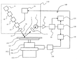
図1は、本発明の第1の実施の形態に係る表面検査装置の全体構成を示す概略図である。
図1は、本発明の第1の実施の形態に係る表面検査装置の全体構成を示す概略図である。
図1において、本実施の形態の表面検査装置は、被検査物の一例である半導体ウエハ100と、半導体ウエハ100を真空吸着するチャック101と、チャック101を半導体ウエハ100と共に回転移動する回転ステージ103及び並進移動する並進ステージ104とから成る被検査物移動ステージ102と、真空チャック101及び被検査物移動ステージ102を垂直方向に移動することにより半導体ウエハ100を垂直方向に移動するZステージ105と、半導体ウエハ100の上方に配置され、その半導体ウエハ100の表面に照明光21を照射し、半導体ウエハ100の表面からの散乱・回折・反射光を検出する照明・検出光学系110と、被検査物移動ステージ102及び照明・検出光学系110の照明・検出動作を制御する照明・検出制御系140とを備えている。
半導体ウエハ100の表面に照明光21を照射し、被検査物移動ステージ102により半導体ウエハ100を回転移動及び並進移動させることにより、半導体ウエハ100の表面を照明光21により走査する。このとき、回転ステージ103が半導体100を回転移動させることにより行われる走査、すなわち回転方向に沿う方向の走査を主走査、並進ステージ104が半導体100を並進移動することにより行われる走査、すなわち主走査に直行する方向の走査を副走査と呼ぶ。
照明・検出光学系110は、レーザ光を生成し射出する光源11と、光源11から射出されたレーザ光を減光し、その光強度を調整する光量調節機構40と、光調節機構40からのレーザ光の光径を調整するビームエキスパンダ41と、ビームエキスパンダ41からのレーザ光を所定のビーム径の平行光束に整形するビーム幅整形光学系14と、ビーム幅整形光学系14の動作を制御するビーム幅制御機構16と、ビーム幅整形光学系14からのレーザ光を照明光21として半導体ウエハ100の表面に照射し、照明スポット3(後の図7参照)を形成するレンズ18とを備えている。
ビーム幅整形光学系14は、照明光21の断面形状を所定の一方向に圧縮して楕円形にする機能を有している。また、ビーム幅制御機構16は、ビーム幅整形光学系14を制御することにより、楕円形に整形された照明光21の断面形状における縦横比を1:1から1:1/8の間で変化させる。なお、照明光21の断面形状(縦横比)によらず、その照明光21全体の強度は一定に保たれる。
照明光21は例えばP偏光であり、被検査物である半導体ウエハ100の表面に、概略、結晶Siに対するブリュースター角で斜入射するように構成されている。このため照明スポット3は概略楕円形状をしており、その長軸を比検査物移動ステージ102の副走査方向、すなわち、主走査方向に直行する方向に向けて形成されている。
ここで、照度が照明スポット3の中心部のeの2乗分の1(eは自然対数の底)に低下する輪郭線の内部を、あらためて照明スポット3と定義する。この照明スポット3の長軸方向の幅をd1、短軸方向の幅をd2とする。ビーム幅整形光学系14において、レーザ光の断面形状が圧縮される方向はこの長径d1の方向に対応しており、短径d2は一定に保たれる。ビーム幅整形光学系14における縦横比の圧縮率が1:1/K(ただし、1≦K≦8)であるとき、d1とd2の関係は次式で表わされる。

また、照明・検出工学系110は、レーリー散乱に従うような微小な異物(異物、傷、欠陥、汚れ等)1に対して効率良くその散乱光(散乱・回折・反射光)を捕捉できるよう、低い仰角で散乱光を集光できるように配置された集光レンズ5と、異物1からの散乱光を検出する光検出器(例えば、光電子増倍管)7とを備えている。なお、本実施例では光検出器7として光電子増倍管を用いているが、異物1からの散乱光を高感度に検出できる光検出器であれば他の検出原理の光検出器であっても良い。
照明・検出制御系140は、増幅器26、A/D変換器30、粒径算出機構120、異物・欠陥判定機構108、異物・欠陥座標検出機構130、及び検査座標検出機構106を備えている。
光検出器7からの散乱光信号は増幅器26で増幅された後、A/D変換器30で予め定められたサンプリング間隔毎にサンプリングされ、デジタルデータに変換される。A/D変換器30によるサンプリング間隔は主走査の1回転の間を概略一定の等角度間隔で刻むように設定されている。異物1に対応する散乱光信号は、その異物1が照明スポット3の短軸方向の幅d2を横切る分の時間幅にわたり持続して発生するため、デジタルデータはこの時間幅に相当するサンプリング点数分にわたる統計演算処理が施される。統計演算処理を施された平均化デジタルデータは異物・欠陥判定機構108で、予め定められた検出閾値と比較され、平均化デジタルデータがその閾値以上であれば、異物・欠陥判定機構108はこの平均化デジタルデータが異物・欠陥よるものだと判定して、その後の平均化デジタルデータの値の変化を監視し、最大値が検出された時点で異物・欠陥判定情報を発生する。異物・欠陥座標検出機構130は、異物・欠陥判定情報が発生すると、検出された異物・欠陥の座標位置を算出する。続いて粒径算出機構120は平均化デジタルデータの最大値から、検出された異物・欠陥の大きさを算出する。この際、同じ大きさの異物・欠陥であっても、そこから得られる平均デジタルデータの大きさは照明スポット3の照度に比例して変化する。なお、ビーム幅整形光学系14によって照明スポット3の面積をK倍だけ変化させるように制御するので、検出された異物・欠陥の大きさを算出する際には、平均化デジタルデータを照明スポット3の面積変化に伴う照度変化分だけ補正して用いる。
被検査物体移動ステージ102は、主走査である回転移動θと副走査である並進移動rを組合せて変化させることで、相対的に照明スポット3を半導体ウエハ100の概略全表面上で螺旋状に走査させる。被検査物体移動ステージ102には、検査中の主走査座標位置θと副走査座標位置rを検出するために、検査座標検出機構106が取り付けてある。なお、本実施の形態においては、主走査座標位置θの検出には光学読み取り式のロータリーエンコーダ(図示せず)を用い、副走査座標位置rには光学読み取り式のリニアエンコーダを用いているが、共に、高精度で角度または直線上の位置が検出できるセンサであれば、他の検出原理を用いたものでも良い。また、照明スポット3の走査は半導体ウエハ100の内周から外周に向かって行うが、逆であっても良い。
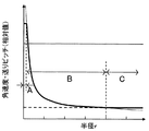
図2は、本発明の第1の実施の形態の被検査物表面における照明スポット3の位置と角速度、及び送りピッチの関係の一例を示す図である。
図2において、縦軸は被検査物移動ステージ102の回転ステージ103による半導体ウエハ100の主走査方向への回転移動速度(角速度)、及び並進ステージ104による半導体100ウエハの副走査方向への並進移動速度、すなわち、回転ステージが1回転する間に並進ステージ104が移動する距離(送りピッチ)を示しており、横軸は、ウエハ100の中心から照明スポット3までの距離(以下、半径と称する)rを示している。また、半導体ウエハ100を、その回転中心からの半径rによって、3つの領域A,B,Cとする。領域Aが最も回転中心に近い領域であり、領域Cが最も回転中心から遠い領域、すなわち、半導体ウエハ100の外縁部である。また、領域Bは領域Aと領域Bの間の領域である。
角速度は、半径rによらず一定の値b1である。
送りピッチは、領域Aにおいては一定値a1であり、領域Bにおいては半径rに概略反比例するように減少し、領域Cにおいては一定値c1である。ここで、領域Aを内周送りピッチ固定領域、領域Bを送りピッチ制御領域、領域Cを外周送りピッチ固定領域と称する。
ここで、送りピッチpが、p>d1であると、半導体ウエハ100上で照明スポット3による螺旋状走査において照明光102が照射されず、検査されない隙間領域ができてしまうので、p≦d1となるよう、d1の大きさも上記pの変化に同期させて、半径rに概略反比例するように制御する。この制御は、ビーム幅制御機構16によりビーム幅整形光学系14を制御することで行う。上記のように主走査回転角速度、副走査送りピッチp、照明スポット3の長径d1を制御する結果、送りピッチ制御領域(領域B)においては、照明スポット3が半径rの位置にあるとき、半導体ウエハ100の表面に対する照明スポット3の主走査方向における相対移動速度(線速度)は角速度×反径rであり、半径rに比例する一方で、副走査の送りピッチpはrに反比例するため、その積である検査面積速度は概略一定となる。また前述のように、平均化デジタルデータは主走査の1回転の間を概略等角度間隔で刻んだサンプリング間隔毎に発生するため、送りピッチ制御領域(領域B)においては、半導体ウエハ100の表面上の単位面積あたりに含まれる平均化デジタルデータの点数は、概略一定となる。
以上のように構成した表面検査装置にいて、半導体ウエハ100の中心から外周までの半径をR、半導体ウエハ100の全体を検査(走査)するのに必要な検査時間をT、主走査回転の総周数をMとし、そのうちの第i周目における送りピッチをpi(mm)、主走査回転速度をωi(r/s)、主走査の1回転に要する時間をΔTi(s)とし、かつ、副走査速度は主走査速度に比べて十分遅いと仮定すると、R及びTはそれぞれ下式のように表すことができる。
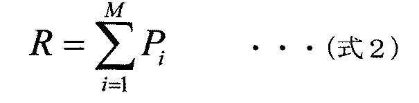

送りピッチpは、前述のように検査中一定に保たれるので、p0を定数としてpi=p0とすると、式1は次式のように表わされる。
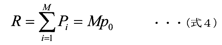
上記式4より、半導体ウエハ100の全体を検査(走査)するのに必要な主走査回転の総周数Mは次式で表わされる。
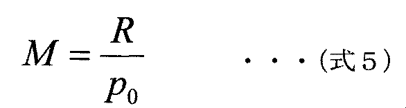
上記式5を式3に代入すると下記の関係式が得られる。

被検査物移動ステージ102の主走査回転機構には回転可能な上限回転速度が存在するので、それをωmaxとすると、上記式6は次式のように表わされる。

すなわち、次式が得られる。

上記式8から、副走査送りピッチが一定である場合、主走査を常に上限回転速度であるωmaxで回転させても、検査時間TはTminより短くすることができないことがわかる。
次に、各数値の一例を用いて、(1)表面検査時間T、(2)検出感度、(3)熱ダメージについて検証する。
(1)表面検査時間T
まず、一例として直径300mmの半導体ウエハ100を考える。この半導体ウエハ100の全領域を検査(走査)するのに必要な検査時間をTとし、内周送りピッチ固定領域(図2の領域A)、送りピッチ制御領域(図2の領域B)、外周送りピッチ固定領域(図2の領域C)の各領域における照明スポット3の長径d1、および主走査回転の第i周目における送りピッチpiを次のように定義する。
・内周送りピッチ固定領域:0mm≦r<12.5mm,d1=0.4mm,pi=0.2mm
・送りピッチ制御領域 :12.5mm≦r<100mm,d1=5/rmm,pi=2.5/rmm
・外周送りピッチ固定領域:100mm≦r<150mm,d1=0.05mm,pi=0.025mm
上記のように定義した各領域における主走査回転の周回数は、
・内周送りピッチ固定領域:1≦i≦62
・送りピッチ制御領域 :63≦i≦2030
・外周送りピッチ固定領域:2031≦i≦4030
となり、主走査回転の総周数Mは、M=4030となる。
まず、一例として直径300mmの半導体ウエハ100を考える。この半導体ウエハ100の全領域を検査(走査)するのに必要な検査時間をTとし、内周送りピッチ固定領域(図2の領域A)、送りピッチ制御領域(図2の領域B)、外周送りピッチ固定領域(図2の領域C)の各領域における照明スポット3の長径d1、および主走査回転の第i周目における送りピッチpiを次のように定義する。
・内周送りピッチ固定領域:0mm≦r<12.5mm,d1=0.4mm,pi=0.2mm
・送りピッチ制御領域 :12.5mm≦r<100mm,d1=5/rmm,pi=2.5/rmm
・外周送りピッチ固定領域:100mm≦r<150mm,d1=0.05mm,pi=0.025mm
上記のように定義した各領域における主走査回転の周回数は、
・内周送りピッチ固定領域:1≦i≦62
・送りピッチ制御領域 :63≦i≦2030
・外周送りピッチ固定領域:2031≦i≦4030
となり、主走査回転の総周数Mは、M=4030となる。
ここで、領域A,B,Cの全てにおいて、d1とpiを
・領域A,B,C:d1=0.05mm ,pi=0.025mm
で一定とした場合には、
M=150/0.025=6000
となる。
・領域A,B,C:d1=0.05mm ,pi=0.025mm
で一定とした場合には、
M=150/0.025=6000
となる。
つまり、角速度一定で主走査回転を行った場合、半導体ウエハ100の全領域においてd1とpiを一定として検査(走査)した場合の検査時間Tと比較して、本実施の形態における表面検査は検査時間を約2/3Tとすることができる。
(2)検出感度
次に、異物の検出感度について考える。本実施の形態においては、外周送りピッチ固定領域(図2の領域C)において、照明スポット3の長径d1、および副走査の送りピッチ(並進移動速度)pを一定に維持する。これらを従来技術と等しく設定した場合、検出感度は当然、従来技術と同等である。なお、この領域内では照明スポット3の照度が一定に保たれるので、線速度が最も遅くなる、最内周の送りピッチ制御領域(図2の領域A)との境界において検出感度が最も高くなる。
次に、異物の検出感度について考える。本実施の形態においては、外周送りピッチ固定領域(図2の領域C)において、照明スポット3の長径d1、および副走査の送りピッチ(並進移動速度)pを一定に維持する。これらを従来技術と等しく設定した場合、検出感度は当然、従来技術と同等である。なお、この領域内では照明スポット3の照度が一定に保たれるので、線速度が最も遅くなる、最内周の送りピッチ制御領域(図2の領域A)との境界において検出感度が最も高くなる。
次に、送りピッチ制御領域(図2の領域B)について考える。前述のように、半導体ウエハ100上にある異物1からの散乱光信号は異物1が照明スポット3の短径d2を横切る分の時間幅にわたり持続して発生すると考えることができるので、この場合、異物1からの散乱光を光検出器7で検出したときに得られる散乱信号の正味信号量Sは、<照明スポットの照度>に比例し、<照明スポット位置での線速度>に反比例することになる。この領域では、<照明スポットの照度>は<照明スポット位置の半径r>に比例して制御され、角速度一定送りの条件下では、<照明スポット位置での線速度>は<照明スポット位置の半径r>に比例するので、2つの要因の比<照明スポットの照度>/<照明スポット位置での線速度>は一定となる。一方、異物1検出時の雑音の大きさNは単位時間当たりの総照射強度の1/2乗、すなわち<照明スポットの照度>×<照明スポットの面積>の積の1/2乗に比例することが知られている。前述のように本実施例では、<照明スポットの面積>を変えても照射光21全体の強度は一定に保たれているので、雑音の大きさNへの影響は一定となる。これらの結果として、この領域内では、外周送りピッチ固定領域(図2の領域C)との境界における検出感度と概略等しい検出感度が得られる。
次に、内周送りピッチ固定領域(図2の領域A)であるが、外周送りピッチ固定領域(図2の領域C)と同様にこの領域では<照明スポットの照度>が一定に保たれるので、最外周の送りピッチ制御領域(図2の領域C)との境界における検出感度が最も低く、この領域全体としてはそれよりも高い検出感度が得られる。すなわち、本実施の形態においては、外周送りピッチ固定領域(図2の領域C)において従来技術と同等の検出感度が得られ、それより内周においても外周部と少なくとも同等以上の検出感度が保たれると言うことができる。
(3)熱ダメージ
次に、検査中に半導体ウエハ100が受ける熱ダメージについて考える。本実施の形態においては、前述のように照明に用いる照射光21全体の強度は概略一定に保たれ、内周部ほど照明スポット3の面積が大きくなっているため、内周部ほど照明スポット3の照度は減少する。検査中に半導体ウエハ100表面が受ける熱ダメージは、熱源である照明スポット3の相対移動線速度が等しい場合には、照明スポット3の照度に概略比例することが知られている。半径rが同一の位置においては、本実施例の技術でも従来技術でも線速度はほぼ等しく、内周部では本実施例の方が照明スポット3の照度が低いため、半導体ウエハ100表面が受ける熱ダメージを低減させることができる。また、熱ダメージは線速度が大きいほど小さくなり、線速度は照明スポット3の位置の半径rに比例して大きくなることから、照明スポット3の照度が一定であれば、熱ダメージは半導体ウエハ100外周部で小さく、内周部ほど大きくなる。前述のように本実施例では内周部ほど照明スポット3の照度が減少するため、熱ダメージは半導体ウエハ外周部で小さく、内周部ほど大きくなることを軽減させることができる。
次に、検査中に半導体ウエハ100が受ける熱ダメージについて考える。本実施の形態においては、前述のように照明に用いる照射光21全体の強度は概略一定に保たれ、内周部ほど照明スポット3の面積が大きくなっているため、内周部ほど照明スポット3の照度は減少する。検査中に半導体ウエハ100表面が受ける熱ダメージは、熱源である照明スポット3の相対移動線速度が等しい場合には、照明スポット3の照度に概略比例することが知られている。半径rが同一の位置においては、本実施例の技術でも従来技術でも線速度はほぼ等しく、内周部では本実施例の方が照明スポット3の照度が低いため、半導体ウエハ100表面が受ける熱ダメージを低減させることができる。また、熱ダメージは線速度が大きいほど小さくなり、線速度は照明スポット3の位置の半径rに比例して大きくなることから、照明スポット3の照度が一定であれば、熱ダメージは半導体ウエハ100外周部で小さく、内周部ほど大きくなる。前述のように本実施例では内周部ほど照明スポット3の照度が減少するため、熱ダメージは半導体ウエハ外周部で小さく、内周部ほど大きくなることを軽減させることができる。
以上のように構成した本実施の形態においては、半導体ウエハ100における副走査の送りピッチ(並進移動速度)を、半導体ウエハ100の主走査における回転中心から照明スポット3までの距離に応じて制御するよう構成したので、表面検査における検出感度の低下、及び熱ダメージの増加を抑制しつつ、検査時間を短縮することができる。
なお、以上のように構成した本実施の形態においては、図2で説明したように、送りピッチ制御領域(図2の領域B)において、送りピッチを半径rに概略反比例するように減少させるよう構成したがこれに限られず、送りピッチが半径rに概略反比例するようにすれば良い。例えば、図3に示すように、送りピッチを半径rに概略反比例するように減少させるようステップ状に変化させた場合においても、本実施の形態と同様の効果を得ることができる。
<第2の実施の形態>
本発明の第2の実施の形態を図4及び図5を参照しつつ説明する。
本発明の第2の実施の形態を図4及び図5を参照しつつ説明する。
図4は本発明の第2の実施の形態に係る表面検査装置の全体構成を示す概略図であり、図5は本発明の第2の実施の形態の被検査物表面における照明スポット3の位置と角速度、及び送りピッチの関係を示す図である。図中、図4及び図5に示す部分と同等のものには同じ符号を付し、説明を省略する。
図4において、本実施の形態の表面検査装置は、増幅器26の周波数帯域を制御する周波数帯域幅制御部27を備えている。
周波数帯域制御部27は、被検査物移動ステージ102における副走査の送りピッチ(並進移動速度)を、半導体ウエハ100の主走査における回転中心から照明スポット3までの距離(半径r)に応じて制御する。前述のように、異物1による散乱・回折・反射光を光検出器7により検出した場合の散乱光信号は、異物1が照明スポット3の短径d2を横切る分の時間幅にわたり持続して発生するが、角速度一定送りの条件下においては線速度が照明スポット3の位置の半径rに比例し、短径d2を変化させない場合には時間幅は半径rに反比例するので、光検出器7からの散乱光信号の時間変化波形を通過させるのに必要な周波数帯域幅Δfは半径rに比例することになる。そこで、周波数帯域幅制御部27は、光検出器7の出力信号(散乱光信号)を増幅する際の周波数帯域幅Δfを照明スポット3の位置の半径rに比例させるよう制御する。
A/D変換器30からのデジタルデータは異物・欠陥判定機構108で、予め定められた検出閾値と比較され、デジタルデータがその閾値以上であれば、異物・欠陥判定機構108はこのデジタルデータが異物・欠陥によるものだと判定して、その後のデジタルデータの値の変化を監視し、最大値が検出された時点で異物・欠陥判定情報を発生する。異物・欠陥座標検出機構130は、異物・欠陥判定情報が発生すると、検出された異物・欠陥の座標位置を算出する。続いて粒径算出機構120はデジタルデータの最大値から、検出された異物・欠陥の大きさを算出する。この際、同じ大きさの異物・欠陥であっても、そこから得られるデジタルデータの大きさは照明スポット3の照度に比例して変化するので、デジタルデータは照明スポット3の面積変化に伴う照度変化分だけ補正して用いる。
図5において、縦軸は被検査物移動ステージ102の回転ステージ103による半導体ウエハ100の主走査方向への回転移動速度(角速度)、及び並進ステージ104による半導体100ウエハの副走査方向への並進移動速度、すなわち、回転ステージが1回転する間に並進ステージ104が移動する距離(送りピッチ)を示しており、横軸は、ウエハ100の中心から照明スポット3までの距離(以下、半径と称する)rを示している。また、半導体ウエハ100を、その回転中心からの半径rによって、3つの領域A,B,Cとする。領域Aが最も回転中心に近い領域であり、領域Cが最も回転中心から遠い領域、すなわち、半導体ウエハ100の外縁部である。また、領域Bは領域Aと領域Bの間の領域である。
角速度は、半径rによらず一定の値b1である。
送りピッチは、領域Aにおいては一定値a1であり、領域Bにおいては半径rの1/2乗に概略反比例するように減少し、領域Cにおいては一定値c1である。ここで、領域Aを内周送りピッチ固定領域、領域Bを送りピッチ制御領域、領域Cを外周送りピッチ固定領域と称する。
次に、各数値の一例を用いて、(1)表面検査時間T、(2)検出感度、(3)熱ダメージについて検証する。
(1)表面検査時間T
まず、一例として直径300mmの半導体ウエハ100を考える。この半導体ウエハ100の全領域を検査(走査)するのに必要な検査時間をTとし、内周送りピッチ固定領域(図5の領域A)、送りピッチ制御領域(図5の領域B)、外周送りピッチ固定領域(図5の領域C)の各領域における照明スポット3の長径d1、および主走査回転の第i周目における送りピッチpiを次のように定義する。
・内周送りピッチ固定領域:0mm≦r<1.5625mm,d1=0.4mm,pi=0.2mm
・送りピッチ制御領域 :1.5625mm≦r<100mm,d1=0.5/r1/2mm,pi=0.25/r1/2mm
・外周送りピッチ固定領域:100mm≦r<150mm,d1=0.05mm,pi=0.025mm
上記のように定義した各領域における主走査回転の周回数は、
・内周送りピッチ固定領域 : 1≦i≦7
・送りピッチ制御領域 : 8≦i≦2668
・外周送りピッチ固定領域 : 2669≦i≦4668
となり、主走査回転の総周数Mは、M=4668となる。
まず、一例として直径300mmの半導体ウエハ100を考える。この半導体ウエハ100の全領域を検査(走査)するのに必要な検査時間をTとし、内周送りピッチ固定領域(図5の領域A)、送りピッチ制御領域(図5の領域B)、外周送りピッチ固定領域(図5の領域C)の各領域における照明スポット3の長径d1、および主走査回転の第i周目における送りピッチpiを次のように定義する。
・内周送りピッチ固定領域:0mm≦r<1.5625mm,d1=0.4mm,pi=0.2mm
・送りピッチ制御領域 :1.5625mm≦r<100mm,d1=0.5/r1/2mm,pi=0.25/r1/2mm
・外周送りピッチ固定領域:100mm≦r<150mm,d1=0.05mm,pi=0.025mm
上記のように定義した各領域における主走査回転の周回数は、
・内周送りピッチ固定領域 : 1≦i≦7
・送りピッチ制御領域 : 8≦i≦2668
・外周送りピッチ固定領域 : 2669≦i≦4668
となり、主走査回転の総周数Mは、M=4668となる。
ここで、領域A,B,Cの全てにおいて、d1とpiを
・領域A,B,C:d1=0.05mm,pi=0.025mm
で一定とした場合には、
M=150/0.025=6000
となる。
・領域A,B,C:d1=0.05mm,pi=0.025mm
で一定とした場合には、
M=150/0.025=6000
となる。
つまり、角速度一定で主走査回転を行った場合、半導体ウエハ100の全領域においてd1とpiを一定として検査(走査)した場合の検査時間Tと比較して、本実施の形態における表面検査は検査時間を約1/1.3Tに短縮することができる。
(2)検出感度
次に、異物の検出感度について考える。
次に、異物の検出感度について考える。
異物1からの散乱光を光検出器7で検出したときに得られる散乱光信号の正味信号量Sは<照明スポットの照度>に比例する一方、雑音の大きさNは<照明スポットの照度>×<照明スポットの面積>×Δfの積の1/2乗に比例する。その結果、正味信号量Sと雑音Nの比であるS/N比は、<照明スポットの照度>/(<照明スポットの面積>×Δf)の1/2乗に比例することになる。照明光21の全体の強度および照明スポット3の短径d2を検査中概略一定に保つものとすると、この場合、照明スポット3の長径d1を照明スポット3位置の半径rの1/2乗に反比例させるよう制御すれば、<照明スポットの照度>は半径rの1/2乗に比例し、<照明スポットの面積>は半径rの1/2乗に反比例し、Δfは半径rに比例するので、S/N比はこれらの因子に関し、概略一定に保たれる。そこで、回転ステージ103は、角速度一定で駆動させるが、並進ステージ104については図5内に示したように、半導体ウエハ100中心部の内周送りピッチ固定領域(図5の領域A)と外縁部の外周送りピッチ固定領域(図5の領域C)の2つの領域を除いた送りピッチ制御領域(図5の領域B)において回転ステージ103が1回転する間に並進ステージ104が移動する送りピッチpを、主走査回転中心と照明スポット3の間の距離の1/2乗、すなわち照明スポット3の位置の半径rの1/2乗に概略反比例するよう駆動させる。また、内周送りピッチ固定領域(図5の領域A)と外周送りピッチ固定領域(図5の領域C)では、pは一定値に固定して駆動させる。また、d1の大きさも上記pの変化に同期させて、照明スポット3の位置の半径rの1/2乗に概略反比例するように制御する。これにより、送りピッチ制御領域(図5の領域B)での検出感度は前述のように、この領域内でほぼ一定となる。また、内周送りピッチ固定領域(図5の領域A)と外周送りピッチ固定領域(図5の領域C)における検出感度については、第一の実施例と同様であるので、外周送りピッチ固定領域(図5の領域C)において従来技術と同等の検出感度が得られ、それより内周においても外周部と少なくとも同等以上の検出感度が保たれると言うことができる。
(3)熱ダメージ
次に、検査中に半導体ウエハ100が受ける熱ダメージについて考える。本実施の形態においては、前述のように照明に用いる照射光21全体の強度は概略一定に保たれ、内周部ほど照明スポット3の面積が大きくなっているため、内周部ほど照明スポット3の照度は減少する。検査中に半導体ウエハ100の表面が受ける熱ダメージは、半導体ウエハ100の外周部で小さく、内周部ほど大きくなることを軽減させることができる。
次に、検査中に半導体ウエハ100が受ける熱ダメージについて考える。本実施の形態においては、前述のように照明に用いる照射光21全体の強度は概略一定に保たれ、内周部ほど照明スポット3の面積が大きくなっているため、内周部ほど照明スポット3の照度は減少する。検査中に半導体ウエハ100の表面が受ける熱ダメージは、半導体ウエハ100の外周部で小さく、内周部ほど大きくなることを軽減させることができる。
その他の構成は第1の実施の形態と同様である。
以上のように構成した本実施の形態においても、半導体ウエハ100における副走査の送りピッチ(並進移動速度)を、半導体ウエハ100の主走査における回転中心から照明スポット3までの距離に応じて制御するよう構成したので、第1の実施の形態と同様に、表面検査における検出感度の低下、及び熱ダメージの増加を抑制しつつ、検査時間を短縮することができる。
<第3の実施の形態>
本発明の第3の実施の形態を図6及び図7を参照しつつ説明する。
本発明の第3の実施の形態を図6及び図7を参照しつつ説明する。
図6は本発明の第3の実施の形態に係る表面検査装置の全体構成を示す概略図である図中、図1に示す部分と同等のものには同じ符号を付し、説明を省略する。本実施の形態の表面検査装置は、第1の実施の形態におけるビーム幅成形光学系14及びビーム幅制御機構16に換えて、ビーム分割機構22及びビーム間隔制御機構23を備え、複数の照明スポット3を半導体ウエハ100上に形成し、その照明スポット3の重複率を、半導体ウエハ100の主走査における回転中心から照明スポット3までの距離が近いほど低く、距離が遠いほど高くなるよう制御するものである。
図6において、ビーム分割機構22は、レーザ光を分割し、複数(例えば、4つ)の照射光21を半導体100の表面に照射して複数(例えば、4つ)の照明スポット3を形成する(図7参照)。
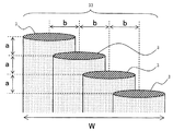
図7は本発明の第3の実施の形態の被検査物表面における照明スポット群33を示す図である。
図7において、縦方向が被検査物移動テーブル102における主走査方向に沿う方向であり、横方向が副走査方向に沿う方向(主走査方向に対して直交する方向)である。
各照明スポット3は、それぞれ主走査方向及び副走査方向における中心を基準とし、主走査方向に沿う方向にa、副走査方向に沿う方向にbの間隔を隔てて等間隔に形成される。間隔bは、主走査に伴って4個の照明スポット3が描く軌跡が重複するよう設定される。複数の照明スポット3による軌跡の副走査方向の幅Wが照明スポット群33の有効照明幅となる。表面検査中、間隔aは概略一定に保たれるが、間隔bはビーム間隔制御機構23により、照明スポット群33の中心位置の半径rに概略反比例するように制御される。これにより、有効照明幅Wは半径rに概略反比例して変化させることができる。
その他の構成は、第1の実施の形態と同様である。
以上のように構成した本実施の形態においても、第1の実施の形態と同様に、表面検査における検出感度の低下、及び熱ダメージの増加を抑制しつつ、検査時間を短縮することができる。
なお、本実施例のビーム間隔制御機構23を、間隔bが照明スポット群33の中心位置の半径rの1/2乗に概略反比例するように制御するよう構成すれば、第2の実施の形態における有効照明幅Wを変化させる手段の代替手段として用いることができることは言うまでもない。
<第4の実施の形態>
本発明の第4の実施の形態を図8を参照しつつ説明する。
本発明の第4の実施の形態を図8を参照しつつ説明する。
図8は本発明の第4の実施の形態に係る表面検査装置の全体構成を示す概略図である図中、図1及び図6に示す部分と同等のものには同じ符号を付し、説明を省略する。本実施の形態の表面検査装置は、第3の実施の形態におけるビーム間隔制御機構23に換えて、ビーム数制御機構24を備え、複数の照明スポット3を半導体ウエハ100上に形成し、その照明スポット3の数を、半導体ウエハ100の主走査における回転中心から照明スポット3までの距離が近いほど多く、距離が遠いほど少なくなるよう制御するものである。
図8において、ビーム分割機構22は、レーザ光を分割し、複数(例えば、4つ)の照射光21を半導体100の表面に照射して複数(例えば、4つ)の照明スポット3を形成する(図7参照)。
本実施の形態においては、表面検査中、間隔a及び間隔bは概略一定に保たれるが、照明スポット群33を構成する複数の照明スポット3の個数は分割ビーム数制御機構24により、照明スポット群33の中心位置の半径rに概略反比例するように制御される。これにより、有効照明幅Wは半径rに概略反比例して変化させることができる。
その他の構成は、第3の実施の形態と同様である。
以上のように構成した本実施の形態においても、第1及び第3の実施の形態と同様に、表面検査における検出感度の低下、及び熱ダメージの増加を抑制しつつ、検査時間を短縮することができる。
なお、本実施例の分割ビーム数制御機構24を、間隔bが照明スポット群33の中心位置の半径rの1/2乗に概略反比例するように制御するよう構成すれば、第2の実施の形態の有効照明幅Wを変化させる手段の代替手段として用いることができることは言うまでもない。
1 異物
5 集光レンズ
7 光検出器
11 光源
14 ビーム幅整形光学系
16 ビーム幅制御機構
18 照射レンズ
21 照明光
26 増幅器
30 A/D変換器
40 光量調節機構
41 ビームエキスパンダ
100 半導体ウエハ
101 チャック
102 被検査物移動ステージ
103 回転ステージ
104 並進ステージ
105 Zステージ
106 検査座標検出機構
108 異物・欠陥判定機構
110 照明・検出光学系
120 粒径算出機構
130 異物・欠陥座標検出機構
140 照明・検出制御系
5 集光レンズ
7 光検出器
11 光源
14 ビーム幅整形光学系
16 ビーム幅制御機構
18 照射レンズ
21 照明光
26 増幅器
30 A/D変換器
40 光量調節機構
41 ビームエキスパンダ
100 半導体ウエハ
101 チャック
102 被検査物移動ステージ
103 回転ステージ
104 並進ステージ
105 Zステージ
106 検査座標検出機構
108 異物・欠陥判定機構
110 照明・検出光学系
120 粒径算出機構
130 異物・欠陥座標検出機構
140 照明・検出制御系
Claims (21)
- 被検査物を主走査として回転移動させ、副走査として並進移動させる披検査物移動手段と、前記被検査物の表面に照明光を照射して、その照明光の照射範囲である照明スポットを形成する照明光照射手段と、前記照明スポットからの散乱・回折・反射光を検出する光検出手段と、前記光検出手段からの検出結果に基づいて前記被検査物の表面上または表面近傍内部に存在する異物を検出する異物検出手段とを備えた表面検査装置を用いる表面検査方法であって、
前記被検査物移動手段における副走査の並進移動速度を、前記被検査物の主走査における回転中心から前記照明スポットまでの距離に応じて制御することを特徴とする表面検査方法。 - 請求項1記載の表面検方法において、
前記被検査物移動手段の主走査における回転速度を一定としたことを特徴とする表面検査方法。 - 請求項1記載の表面検査方法において、
前記被検査物移動手段における副走査の並進移動速度を、前記被検査物の主走査における回転中心から前記照明スポットまでの距離が近いほど大きく、距離が遠いほど小さくなるよう制御することを特徴とする表面検査方法。 - 請求項1記載の表面検査方法において、
前記照明スポットにおける前記主走査方向に直交する方向の径を、前記被検査物の主走査における回転中心から前記照明スポットまでの距離が近いほど大きく、距離が遠いほど小さくなるよう制御することを特徴とする表面検査方法。 - 請求項1記載の表面検査方法において、
前記被検査物移動手段における副走査の並進移動速度を、前記被検査物の主走査における回転中心から前記照明スポットまでの距離に概略反比例するよう制御することを特徴とする表面検査方法。 - 請求項1記載の表面検査方法において、
前記照明スポットにおける前記主走査方向に直交する方向の径を、前記被検査物の主走査における回転中心から前記照明スポットまでの距離に概略反比例するよう制御することを特徴とする表面検査方法。 - 請求項1記載の表面検査方法において、
前記被検査物移動手段における副走査の並進移動速度を、前記被検査物の主走査における回転中心から前記照明スポットまでの距離の1/2乗に概略反比例するよう制御することを特徴とする表面検査方法。 - 請求項1記載の表面検査方法において、
前記照明スポットにおける前記主走査方向に直交する方向の径を、前記被検査物の主走査における回転中心から前記照明スポットまでの距離の1/2乗に概略反比例するよう制御することを特徴とする表面検査方法。 - 請求項1記載の表面検査方法において、
前記照明スポットは楕円形状であることを特徴とする表面検査方法。 - 請求項1記載の表面検査方法において、
前記照明スポットは、前記被検査物の主走査により該照明スポットにより走査される前記被検査物表面の軌跡の少なくとも一部が重複するように配置された複数の照明スポットから成り、前記複数の照明スポットの数を、前記被検査物の主走査における回転中心から前記照明スポットまでの距離が近いほど多く、距離が遠いほど少なくなるよう制御することを特徴とする表面検査方法。 - 請求項1記載の表面検査方法において、
前記照明スポットは、前記被検査物の主走査方向に直行する方向にずらして配置され、かつ、前記主走査により各照明スポットにより走査される前記被検査物表面の軌跡の少なくとも一部が重複するように配置された複数の照明スポットから成り、前記複数の照明スポットの重複する比率を、前記被検査物の主走査における回転中心から前記照明スポットまでの距離が近いほど小さく、距離が遠いほど大きくなるよう制御することを特徴とする表面検査方法。 - 被検査物を主走査として回転移動させ、副走査として並進移動させる披検査物移動手段と、前記被検査物の表面に照明光を照射して、その照明光の照射範囲である照明スポットを形成する照明光照射手段と、前記照明スポットからの散乱・回折・反射光を検出する光検出手段と、前記光検出手段からの検出結果に基づいて前記被検査物の表面上または表面近傍内部に存在する異物を検出する異物検出手段とを備えた表面検査装置を用いる表面検査方法であって、
前記被検査物が前記主走査より1回転する間に前記照明スポットにより走査される前記被検査物の面積が略一定となるように制御することを特徴とすることを特徴とする表面検査方法。 - 請求項12記載の表面検方法において、
前記被検査物移動手段の主走査における回転速度を一定としたことを特徴とする表面検査方法。 - 被検査物を主走査として回転移動させ、副走査として並進移動させる披検査物移動手段と、前記被検査物の表面に照明光を照射して、その照明光の照射範囲である照明スポットを形成する照明光照射手段と、前記照明スポットからの散乱・回折・反射光を検出する光検出手段と、前記光検出手段からの検出結果に基づいて前記被検査物の表面上または表面近傍内部に存在する異物を検出する異物検出手段とを備えた表面検査装置を用いる表面検査方法であって、
前記光検出手段からの検出結果のデータ量が、前記被検査物の単位面積あたり略一定となるように制御することを特徴とすることを特徴とする表面検査方法。 - 請求項14記載の表面検方法において、
前記被検査物移動手段の主走査における回転速度を一定としたことを特徴とする表面検査方法。 - 被検査物を主走査として回転移動させ、副走査として並進移動させる披検査物移動手段と、
前記被検査物の表面に照明光を照射して、その照明光の照射範囲である照明スポットを形成する照明光照射手段と、
前記照明スポットからの散乱・回折・反射光を検出する光検出手段と、
前記光検出手段からの検出結果に基づいて前記被検査物の表面上または表面近傍内部に存在する異物を検出する異物検出手段と、
前記被検査物移動手段における副走査の並進移動速度を、前記被検査物の主走査における回転中心から前記照明スポットまでの距離に応じて制御する手段と
を備えたことを特徴とする表面検査装置。 - 被検査物を主走査として回転移動させ、副走査として並進移動させる披検査物移動手段と、
前記被検査物の表面に照明光を照射して、その照明光の照射範囲である照明スポットを形成する照明光照射手段と、
前記照明スポットからの散乱・回折・反射光を検出する光検出手段と、
前記光検出手段からの検出結果に基づいて前記被検査物の表面上または表面近傍内部に存在する異物を検出する異物検出手段と、
前記被検査物が前記主走査より1回転する間に前記照明スポットにより走査される前記被検査物の面積が略一定となるように制御する手段と
を備えたことを特徴とする表面検査装置。 - 被検査物を主走査として回転移動させ、副走査として並進移動させる披検査物移動手段と、
前記被検査物の表面に照明光を照射して、その照明光の照射範囲である照明スポットを形成する照明光照射手段と、
前記照明スポットからの散乱・回折・反射光を検出する光検出手段と、
前記光検出手段からの検出結果に基づいて前記被検査物の表面上または表面近傍内部に存在する異物を検出する異物検出手段と、
前記光検出手段からの検出結果のデータ量が、前記被検査物の単位面積あたり略一定となるように制御する手段と
を備えたことを特徴とする表面検査装置。 - 請求項16記載の表面検装置において、
前記被検査物移動手段の主走査における回転速度を一定とし、
前記被検査物移動手段における副走査の並進移動速度を、前記被検査物の主走査における回転中心から前記照明スポットまでの距離が近いほど大きく、距離が遠いほど小さくなるよう制御する手段と、
前記照明スポットにおける前記主走査方向に直交する方向の径を、前記被検査物の主走査における回転中心から前記照明スポットまでの距離が近いほど大きく、距離が遠いほど小さくなるよう制御する手段と
を備えたことを特徴とする表面検査装置。 - 請求項16記載の表面検査装置において、
前記被検査物移動手段の主走査における回転速度を一定とし、
前記被検査物移動手段における副走査の並進移動速度を、前記被検査物の主走査における回転中心から前記照明スポットまでの距離に概略反比例するよう制御する手段と、
前記照明スポットにおける前記主走査方向に直交する方向の径を、前記被検査物の主走査における回転中心から前記照明スポットまでの距離に概略反比例するよう制御する手段と
を備えたことを特徴とする表面検査装置。 - 請求項16記載の表面検査方法において、
前記被検査物移動手段の主走査における回転速度を一定とし、
前記被検査物移動手段における副走査の並進移動速度を、前記被検査物の主走査における回転中心から前記照明スポットまでの距離の1/2乗に概略反比例するよう制御する手段と、
前記照明スポットにおける前記主走査方向に直交する方向の径を、前記被検査物の主走査における回転中心から前記照明スポットまでの距離の1/2乗に概略反比例するよう制御する手段と
を備えたことを特徴とする表面検査装置。
Priority Applications (2)
| Application Number | Priority Date | Filing Date | Title |
|---|---|---|---|
| US13/202,681 US8493557B2 (en) | 2009-03-06 | 2010-01-22 | Surface inspecting apparatus and surface inspecting method |
| US13/929,030 US9046499B2 (en) | 2009-03-06 | 2013-06-27 | Surface inspecting apparatus and surface inspecting method |
Applications Claiming Priority (2)
| Application Number | Priority Date | Filing Date | Title |
|---|---|---|---|
| JP2009-053921 | 2009-03-06 | ||
| JP2009053921A JP5213765B2 (ja) | 2009-03-06 | 2009-03-06 | 表面検査装置及び表面検査方法 |
Related Child Applications (2)
| Application Number | Title | Priority Date | Filing Date |
|---|---|---|---|
| US13/202,681 A-371-Of-International US8493557B2 (en) | 2009-03-06 | 2010-01-22 | Surface inspecting apparatus and surface inspecting method |
| US13/929,030 Continuation US9046499B2 (en) | 2009-03-06 | 2013-06-27 | Surface inspecting apparatus and surface inspecting method |
Publications (1)
| Publication Number | Publication Date |
|---|---|
| WO2010100973A1 true WO2010100973A1 (ja) | 2010-09-10 |
Family
ID=42709536
Family Applications (1)
| Application Number | Title | Priority Date | Filing Date |
|---|---|---|---|
| PCT/JP2010/050851 Ceased WO2010100973A1 (ja) | 2009-03-06 | 2010-01-22 | 表面検査装置及び表面検査方法 |
Country Status (3)
| Country | Link |
|---|---|
| US (2) | US8493557B2 (ja) |
| JP (1) | JP5213765B2 (ja) |
| WO (1) | WO2010100973A1 (ja) |
Families Citing this family (6)
| Publication number | Priority date | Publication date | Assignee | Title |
|---|---|---|---|---|
| JP5295160B2 (ja) * | 2010-03-30 | 2013-09-18 | 株式会社日立ハイテクノロジーズ | 表面検査装置及び表面検査方法 |
| US8885158B2 (en) * | 2011-03-10 | 2014-11-11 | Kla-Tencor Corporation | Surface scanning inspection system with adjustable scan pitch |
| US8786850B2 (en) * | 2012-10-29 | 2014-07-22 | Kla-Tencor Corporation | Illumination energy management in surface inspection |
| CN107884318B (zh) * | 2016-09-30 | 2020-04-10 | 上海微电子装备(集团)股份有限公司 | 一种平板颗粒度检测方法 |
| JP6581614B2 (ja) * | 2017-03-14 | 2019-09-25 | 株式会社サイオクス | 半導体構造体の製造方法、検査方法、およびプログラム |
| JP7071181B2 (ja) * | 2018-03-20 | 2022-05-18 | キヤノン株式会社 | 異物検査装置、成形装置および物品製造方法 |
Citations (5)
| Publication number | Priority date | Publication date | Assignee | Title |
|---|---|---|---|---|
| JPS5328772U (ja) * | 1976-08-18 | 1978-03-11 | ||
| JPS61133843A (ja) * | 1984-12-05 | 1986-06-21 | Hitachi Electronics Eng Co Ltd | 表面検査装置 |
| JPS6333651A (ja) * | 1986-07-28 | 1988-02-13 | Seiko Epson Corp | 光デイスク検査装置 |
| JP2000329709A (ja) * | 1999-03-31 | 2000-11-30 | Ade Optical Syst Corp | ワークピース表面の欠陥検査装置及び方法 |
| JP2007309713A (ja) * | 2006-05-17 | 2007-11-29 | Hitachi High-Technologies Corp | 光学式検査方法及び光学式検査装置 |
Family Cites Families (7)
| Publication number | Priority date | Publication date | Assignee | Title |
|---|---|---|---|---|
| CH595489A5 (ja) | 1976-08-20 | 1978-02-15 | Rueti Ag Maschf | |
| US4727325A (en) * | 1985-10-16 | 1988-02-23 | Hitachi, Ltd. | NMR imaging method |
| US7548308B2 (en) | 2005-05-11 | 2009-06-16 | Kla-Tencor Corporation | Illumination energy management in surface inspection |
| JP4741986B2 (ja) | 2006-06-30 | 2011-08-10 | 株式会社日立ハイテクノロジーズ | 光学式検査方法および光学式検査装置 |
| JP5279992B2 (ja) | 2006-07-13 | 2013-09-04 | 株式会社日立ハイテクノロジーズ | 表面検査方法及び装置 |
| JP5319876B2 (ja) * | 2006-07-31 | 2013-10-16 | 株式会社日立ハイテクノロジーズ | 表面検査装置及び表面検査方法 |
| JP2008032582A (ja) | 2006-07-31 | 2008-02-14 | Hitachi High-Technologies Corp | 異物・欠陥検査装置および異物欠陥・検査方法 |
-
2009
- 2009-03-06 JP JP2009053921A patent/JP5213765B2/ja not_active Expired - Fee Related
-
2010
- 2010-01-22 US US13/202,681 patent/US8493557B2/en not_active Expired - Fee Related
- 2010-01-22 WO PCT/JP2010/050851 patent/WO2010100973A1/ja not_active Ceased
-
2013
- 2013-06-27 US US13/929,030 patent/US9046499B2/en not_active Expired - Fee Related
Patent Citations (5)
| Publication number | Priority date | Publication date | Assignee | Title |
|---|---|---|---|---|
| JPS5328772U (ja) * | 1976-08-18 | 1978-03-11 | ||
| JPS61133843A (ja) * | 1984-12-05 | 1986-06-21 | Hitachi Electronics Eng Co Ltd | 表面検査装置 |
| JPS6333651A (ja) * | 1986-07-28 | 1988-02-13 | Seiko Epson Corp | 光デイスク検査装置 |
| JP2000329709A (ja) * | 1999-03-31 | 2000-11-30 | Ade Optical Syst Corp | ワークピース表面の欠陥検査装置及び方法 |
| JP2007309713A (ja) * | 2006-05-17 | 2007-11-29 | Hitachi High-Technologies Corp | 光学式検査方法及び光学式検査装置 |
Also Published As
| Publication number | Publication date |
|---|---|
| US9046499B2 (en) | 2015-06-02 |
| JP2010210279A (ja) | 2010-09-24 |
| US20140009756A1 (en) | 2014-01-09 |
| US8493557B2 (en) | 2013-07-23 |
| JP5213765B2 (ja) | 2013-06-19 |
| US20120044505A1 (en) | 2012-02-23 |
Similar Documents
| Publication | Publication Date | Title |
|---|---|---|
| JP4959225B2 (ja) | 光学式検査方法及び光学式検査装置 | |
| JP4703671B2 (ja) | 表面検査方法およびそれを用いた検査装置 | |
| JP5355922B2 (ja) | 欠陥検査装置 | |
| JP5213765B2 (ja) | 表面検査装置及び表面検査方法 | |
| US7791721B2 (en) | Surface inspection with variable digital filtering | |
| TWI567380B (zh) | 具有可獨立調整之掃描間距的表面掃描檢查系統 | |
| TWI625519B (zh) | 表面檢驗方法及系統 | |
| JP5463943B2 (ja) | 画像データ処理方法および画像作成方法 | |
| US8101935B2 (en) | Inspection apparatus and inspection method | |
| CN1720742A (zh) | 用于检测诸如轧制/拉制金属条的工件上的表面缺陷的装置和方法 | |
| JP5349742B2 (ja) | 表面検査方法及び表面検査装置 | |
| WO2016009920A1 (ja) | 基板の検査装置及び基板の検査方法 | |
| JP5564807B2 (ja) | 欠陥検査装置及び欠陥検査方法 | |
| JP5295160B2 (ja) | 表面検査装置及び表面検査方法 | |
| US8547547B2 (en) | Optical surface defect inspection apparatus and optical surface defect inspection method | |
| US20130286386A1 (en) | Optical surface defect inspection apparatus and optical surface defect inspection method | |
| JP5010881B2 (ja) | 検査装置および検査方法 | |
| CN114199891B (zh) | 一种检测方法和检测设备 | |
| JP5689918B2 (ja) | 試料の状態を評価するための装置及び方法 | |
| JP5668113B2 (ja) | 欠陥検査装置 | |
| JP2015068732A (ja) | 磁気メディアの光学式検査方法及びその装置 | |
| JP2011232267A (ja) | 半導体ウェーハの表面検査方法および表面検査装置、ならびに半導体ウェーハの製造方法 |
Legal Events
| Date | Code | Title | Description |
|---|---|---|---|
| 121 | Ep: the epo has been informed by wipo that ep was designated in this application |
Ref document number: 10748570 Country of ref document: EP Kind code of ref document: A1 |
|
| NENP | Non-entry into the national phase |
Ref country code: DE |
|
| WWE | Wipo information: entry into national phase |
Ref document number: 13202681 Country of ref document: US |
|
| 122 | Ep: pct application non-entry in european phase |
Ref document number: 10748570 Country of ref document: EP Kind code of ref document: A1 |