WO2010097997A1 - 磁性発振素子 - Google Patents
磁性発振素子 Download PDFInfo
- Publication number
- WO2010097997A1 WO2010097997A1 PCT/JP2009/070045 JP2009070045W WO2010097997A1 WO 2010097997 A1 WO2010097997 A1 WO 2010097997A1 JP 2009070045 W JP2009070045 W JP 2009070045W WO 2010097997 A1 WO2010097997 A1 WO 2010097997A1
- Authority
- WO
- WIPO (PCT)
- Prior art keywords
- magnetic
- oscillation
- magnetization
- free layer
- layer
- Prior art date
- Legal status (The legal status is an assumption and is not a legal conclusion. Google has not performed a legal analysis and makes no representation as to the accuracy of the status listed.)
- Ceased
Links
Images






Classifications
-
- H—ELECTRICITY
- H03—ELECTRONIC CIRCUITRY
- H03B—GENERATION OF OSCILLATIONS, DIRECTLY OR BY FREQUENCY-CHANGING, BY CIRCUITS EMPLOYING ACTIVE ELEMENTS WHICH OPERATE IN A NON-SWITCHING MANNER; GENERATION OF NOISE BY SUCH CIRCUITS
- H03B15/00—Generation of oscillations using galvano-magnetic devices, e.g. Hall-effect devices, or using superconductivity effects
- H03B15/006—Generation of oscillations using galvano-magnetic devices, e.g. Hall-effect devices, or using superconductivity effects using spin transfer effects or giant magnetoresistance
-
- H—ELECTRICITY
- H10—SEMICONDUCTOR DEVICES; ELECTRIC SOLID-STATE DEVICES NOT OTHERWISE PROVIDED FOR
- H10N—ELECTRIC SOLID-STATE DEVICES NOT OTHERWISE PROVIDED FOR
- H10N50/00—Galvanomagnetic devices
- H10N50/10—Magnetoresistive devices
Definitions
- the present invention relates to a microwave oscillator.
- the magnetoresistive element such as GMR elements and TMR elements (MR elements), by energizing the large DC current I than a certain threshold current I C, the spin torque is applied to the free layer magnetization in the MR elements, the number-number It is known that a steady magnetization vibration of 10 GHz is excited (see, for example, Non-Patent Documents 1 and 2).
- This magnetization vibration is converted into high frequency power by the MR effect.
- a typical element size in which this phenomenon is seen is about 100 nm ⁇ 100 nm.
- This element is called a magnetic oscillation element because the origin of the microwave is derived from magnetic oscillation.
- the origin of magnetization oscillation is spin torque, it is also called a spin torque oscillator (Spin-Torque Oscillator).
- the magnetic oscillation element As an application of the magnetic oscillation element, an application utilizing the fact that it is a micro size oscillator has been devised. One of them is to use a magnetic oscillation element as a reference clock in a portable electronic device.
- the conventional crystal oscillator is replaced with a magnetic oscillation element, not only the space for the reference clock can be reduced, but also the reference clock can be integrated in a single transmission / reception circuit chip. It can also be used as a local oscillator in a heterodyne detector so that RF spectrum analysis can be performed on a single chip.
- the magnetic oscillation element is also an oscillating magnetic field generator derived from magnetization vibration, an application utilizing the oscillating magnetic field has been devised.
- One of them relates to wireless communication, and is an application in which a magnetic oscillation element is applied as a wireless communication transmitter for transferring data between individual components in a computer.
- Main characteristics required for the magnetic oscillation element for various applications described above are that a high-frequency output is efficiently extracted from the element, a high output in the ⁇ W order, and an oscillation frequency is stable. Elements.
- the element resistance is desired to be about 100 ⁇ . This is because the characteristic impedance of many high-frequency devices is designed and standardized at about 50 ⁇ , and the magnetic oscillation element as the high-frequency device must also conform to such a standard.
- a typical element size in which magnetization vibration is excited is about 100 nm ⁇ 100 nm. Therefore, RA (product of element resistance and junction area) of the magnetic oscillation element is 1 ⁇ ⁇ ⁇ m 2 or less. Is required.
- RA 1 ⁇ ⁇ ⁇ m 2 or less
- TMR element which was not possible in the past, in recent years, the technology for forming a spacer layer with a film thickness of about 2 to 3 atoms has advanced, and it is possible to reduce RA to 1 ⁇ ⁇ ⁇ m 2 or less. is there.
- MgO-MTJ magnetic tunnel junction films having MgO barriers have attracted attention as elements with high MR ratios. So-called MgO-MTJ. MgO-MTJ has an MR ratio of about several hundred percent, and it is well known that an output of about several hundred nW is actually extracted from the magnetization vibration in MgO-MTJ.
- the voltage applied to the device is about 0.1 V or less.
- a magnetic oscillating device that satisfies the last one factor that the oscillation frequency is stable has not been disclosed yet. That is, development of a magnetic oscillation element that satisfies all of the above three elements, specifically, a magnetic oscillation element that satisfies J ⁇ 1.0 ⁇ 10 7 A / cm 2 and has a stable oscillation frequency is required. ing.
- the present invention proposes a magnetic oscillation element that has a high output and a long life and has a stable oscillation frequency.
- a magnetic oscillation element includes a magnetic free layer having a variable magnetization direction, a magnetic pinned layer having an invariable magnetization direction, a spacer layer disposed between the magnetic free layer and the magnetic pinned layer, and the magnetic layer.
- a magnetic field generation unit that applies an external magnetic field to the free layer.
- the magnetic free layer and the magnetic pinned layer have a magnetization direction parallel to a bonding surface between them and the spacer layer.
- the magnetic free layer has uniaxial magnetic anisotropy and causes magnetization oscillation when a current larger than the oscillation threshold current flows through the magnetic free layer.
- the magnetic field generator has a magnitude of the external magnetic field in a direction to cancel out the shift amount of the oscillation frequency caused by the demagnetizing field due to the magnetization vibration and the shift amount of the oscillation frequency caused by the magnetic field due to the uniaxial magnetic anisotropy. And control the direction.
- An angle ⁇ between the direction of the center of magnetization vibration of the magnetic free layer and the magnetization direction of the magnetic pinned layer is in the range of 0 ° ⁇ ⁇ ⁇ 70 ° and 110 ° ⁇ ⁇ ⁇ 180 °.
- a magnetic oscillation element having a high output and a long life and having a stable oscillation frequency can be realized.
- the magnetic oscillation element is composed of a magnetoresistive effect element, and the magnetic free layer and the magnetic pinned layer of the magnetoresistive effect element each have in-plane magnetization.
- in-plane magnetization means that the magnetization direction is parallel to the junction surface between the magnetic free layer and the spacer layer, and with respect to the magnetic pinned layer, in-plane magnetization means that the magnetization direction is magnetic. It means that it is parallel to the joint surface between the pinned layer and the spacer layer.
- the magnetic oscillation element according to the example of the present invention utilizes a phenomenon in which magnetization oscillation occurs when a current in the magnetoresistive element is passed.
- the frequency of this magnetization vibration is the oscillation frequency of the magnetic oscillation element.
- a certain current is a current having a current density larger than the oscillation threshold current density.
- the shift amount of the oscillation frequency caused by the demagnetizing field due to the magnetization vibration of the magnetic free layer and the shift amount of the oscillation frequency caused by the magnetic field due to the uniaxial magnetic anisotropy of the magnetic free layer are calculated.
- An external magnetic field acting in the canceling direction is applied to the magnetic oscillation element.
- the spectral oscillation line width ⁇ f which is an index of oscillation frequency stability, can be made very narrow.
- the angle ⁇ formed by the magnetization direction that is the center of the magnetization vibration of the magnetic free layer and the magnetization direction of the magnetic pinned layer is 0 ° ⁇ ⁇ ⁇ 70 ° and 110 ° ⁇ ⁇ ⁇ 180 °. Set within the range.
- the oscillation in the range of 0 ° ⁇ ⁇ ⁇ 70 ° is an oscillation in which the magnetization directions of the magnetic free layer and the magnetic pinned layer are parallel (parallel oscillation), and the oscillation in the range of 110 ° ⁇ ⁇ ⁇ 180 ° is This is an oscillation in which the magnetization directions of the magnetic free layer and the magnetic pinned layer are antiparallel (antiparallel oscillation).
- the parallel magnetization direction means that the angle ⁇ between the oscillation center magnetization direction of the magnetic free layer and the magnetization direction of the magnetic pinned layer is in the range of 0 ° ⁇ ⁇ ⁇ 90 °, and the magnetization direction is antiparallel. Means that the angle ⁇ formed by the magnetization center magnetization direction of the magnetic free layer and the magnetization direction of the magnetic pinned layer is in the range of 90 ° ⁇ ⁇ ⁇ 180 °.
- the spacer layer is made of MgO, a higher output and higher frequency output can be obtained.
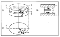
- Embodiment 1 and 2 show a magnetic oscillation element according to the first embodiment.
- 1A is a bird's eye view
- FIG. 1B is a cross-sectional view
- FIG. 1C is a projection view.
- FIG. 2 shows an example of the positional relationship between the magnetic oscillation element and the magnetic field generation unit.
- the magnetic oscillation element includes a magnetic free layer 1, a spacer layer 2, a magnetic pinned layer 3, and a pair of electrodes 4.
- the magnetic free layer 1 is made of a ferromagnetic material
- the spacer layer 2 is made of a nonmagnetic layer (for example, MgO).
- the magnetic free layer 1 has in-plane magnetization and uniaxial magnetic anisotropy.
- the direction 5 of uniaxial magnetic anisotropy of the magnetic free layer 1 is illustrated in FIGS.
- Uniaxial magnetic anisotropy can be generated by depositing a material having high magnetocrystalline anisotropy in a uniform magnetic field, or by annealing in a uniform magnetic field after deposition. This is called crystal magnetic anisotropy. Uniaxial magnetic anisotropy can also be generated by making the ferromagnetic material rectangular or elliptical. This is called shape magnetic anisotropy.
- the planar shape of the magnetic free layer 1 is, for example, an ellipse whose major axis is the uniaxial magnetic anisotropy direction 5 of the magnetic free layer 1.
- the planar shape of the magnetic pinned layer 3 may be the same as or different from the planar shape of the magnetic free layer 1.
- planar shape of the magnetic free layer 1 means the shape of the magnetic free layer 1 in a plane parallel to the joint surface between the magnetic free layer 1 and the spacer layer 2.
- planar shape of the magnetic pinned layer 3 means the shape of the magnetic pinned layer 3 in a plane parallel to the joint surface between the magnetic pinned layer 3 and the spacer layer 2.
- a current (current having a current density larger than the oscillation threshold current density) I larger than the oscillation threshold current (current having the oscillation threshold current density) Ic is passed between the pair of electrodes 4. Then, magnetization vibration of the magnetic free layer 1 occurs.
- the magnetic field generation unit 7 causes the magnetic oscillation element to oscillate due to the magnetic field due to the shift amount of the oscillation frequency due to the demagnetizing field in the magnetization oscillation of the magnetic free layer 1 and the uniaxial magnetic anisotropy of the magnetic free layer 1.
- An external magnetic field acting in a direction that cancels out the frequency shift amount is applied.
- the spectral oscillation line width ⁇ f becomes very narrow, and the value of the oscillation frequency can be stabilized.
- the angle ⁇ formed by the magnetization direction 6 that is the center of the magnetization vibration of the magnetic free layer 1 and the magnetization direction (invariable) M2 of the magnetic pinned layer 3 is 0 °.
- ⁇ ⁇ ⁇ 70 ° and 110 ° ⁇ ⁇ ⁇ 180 ° are set.
- the spectral oscillation line width ⁇ f which is an index of the oscillation frequency stability, can be expressed by the following equation, as in the case of a conventional oscillator such as a laser or an electric circuit oscillator.
- ⁇ fres is the resonator line width
- kBT is the thermal energy
- Eosci is the magnetization vibration energy.
- ⁇ is a factor representing the magnitude of the frequency shift effect and the sign of the shift. Depending on whether ⁇ is positive or negative, for example, if ⁇ > 0, the frequency decreases (red shift), and if ⁇ ⁇ 0, the frequency increases (blue shift).
- Equation (1) indicates that the oscillation line width ⁇ f increases as the frequency shift effect
- is large, it means that the frequency stability is deteriorated. Therefore, ⁇ 0 is the most ideal situation for the frequency to become stable.
- the red shift effect ( ⁇ > 0) due to the demagnetizing field and the blue shift effect ( ⁇ ⁇ 0) due to the magnetic field due to uniaxial magnetic anisotropy coexist.
- the line width ⁇ f is narrowed, and a stable frequency (magnetization vibration) can be obtained.
- 5 and 6 show conditions for obtaining the simulation result of FIG.
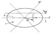
- the direction 6 that is the center of the magnetization vibration of the magnetization M1 of the magnetic free layer 1 is perpendicular (90 °) to the direction 5 of uniaxial magnetic anisotropy of the magnetic free layer 1 and is uniaxial magnetic. It is greater than 45 ° with respect to the anisotropic direction 5.
- the direction of the external magnetic field Hext is parallel to the direction 6 that is the center of the magnetization oscillation of the magnetization M1 of the magnetic free layer 1.
- the direction 6 that becomes the center of the magnetization vibration of the magnetization M1 of the magnetic free layer 1 is parallel (0 °) to the direction 5 of uniaxial magnetic anisotropy of the magnetic free layer 1. Yes, smaller than 45 ° with respect to the direction 5 of uniaxial magnetic anisotropy.
- the direction of the external magnetic field Hext is parallel to the direction 6 that is the center of the magnetization oscillation of the magnetization M1 of the magnetic free layer 1.
- a curve 10 is a simulation result under the conditions of FIG. 5.
- Hext 380 [Oe]
- ⁇ 0
- the oscillation frequency shift amount due to the demagnetizing field due to magnetization oscillation (red shift) Effect) and the shift amount of the oscillation frequency (blue shift effect) caused by the magnetic field due to uniaxial magnetic anisotropy cancel each other.
- the difference in these behaviors is that the direction 6 that is the center of the magnetization vibration of the magnetization M1 of the magnetic free layer 1 is greater than 45 ° with respect to the direction 5 of uniaxial magnetic anisotropy of the magnetic free layer 1, or , Small or depends on.
- the reason why the angle of 45 ° is the boundary value is that the direction of the magnetic field due to the uniaxial magnetic anisotropy with respect to the magnetization M1 of the magnetic free layer 1 is reversed at that angle.
- the oscillation caused by the magnetic field due to the amount of oscillation frequency shift caused by the demagnetizing field in the magnetization oscillation of the magnetic free layer 1 and the uniaxial magnetic anisotropy of the magnetic free layer 1 This is realized by generating an external magnetic field Hext in a direction that cancels out the frequency shift amount.
- the thickness of the magnetic free layer (the width of the magnetic free layer in the direction perpendicular to the interface between the magnetic free layer and the spacer layer) d is 2 nm
- the saturation magnetization MS is 600 emu / cm 3
- the spin polarization P is The magnitude Hext of the external magnetic field was 0.08 ⁇ 4 ⁇ MS
- the magnitude Hk of the magnetic field due to uniaxial magnetic anisotropy was 0.02 ⁇ 4 ⁇ MS.
- the simulation of FIG. 7 relates to oscillation (parallel oscillation) in which the magnetization directions of the magnetic free layer and the magnetic pinned layer are parallel. According to the result, within the range of 0 ° ⁇ ⁇ ⁇ 90 °, the oscillation threshold current density increases as ⁇ increases.
- One of the objects of the present invention is to make the current density of the current passed through the magnetic oscillation element, that is, the oscillation threshold current density J smaller than 1.0 ⁇ 10 7 A / cm 2 . Therefore, it can be understood that 0 ° ⁇ ⁇ ⁇ 70 ° may be satisfied for this purpose.
- the simulation of FIG. 8 relates to oscillation (antiparallel oscillation) in which the magnetization directions of the magnetic free layer and the magnetic pinned layer are antiparallel.
- the oscillation threshold current density increases as ⁇ decreases.
- the oscillation threshold current density increases as ⁇ ′ increases in the range of 0 ° ⁇ ⁇ ′ ⁇ 90 °, as in FIG. Therefore, if 0 ° ⁇ ⁇ ′ ⁇ 70 °, the oscillation threshold current density J can be made smaller than 1.0 ⁇ 10 7 A / cm 2 .
- 0 ° ⁇ ⁇ ′ ⁇ 70 ° is equivalent to 110 ° ⁇ ⁇ 180 °.
- Equation (2) is an amount that is extremely small when ⁇ 90 ° because it is proportional to cos ⁇ with respect to the magnetization M1 of the in-plane magnetization free layer and the magnetization M2 of the in-plane magnetization pinned layer.
- the amount of oscillation frequency shift caused by the demagnetizing field due to the magnetization oscillation of the magnetic free layer and the uniaxial magnetic anisotropy of the magnetic free layer By generating the external magnetic field in a direction that cancels out the shift amount of the oscillation frequency caused by the magnetic field due to the nature, the stability of the oscillation frequency can be improved.
- ⁇ The stability of the oscillation frequency can be further improved by setting it to 0.
- the angle ⁇ between the magnetization direction that becomes the center of the magnetization vibration of the magnetic free layer and the magnetization direction of the magnetic pinned layer is set within the ranges of 0 ° ⁇ ⁇ ⁇ 70 ° and 110 ° ⁇ ⁇ ⁇ 180 °.
- the magnetization oscillation of the magnetic free layer can be excited with a current density smaller than 1.0 ⁇ 10 7 A / cm 2 , and a high-power and long-life magnetic oscillation element can be obtained.
- the spacer layer is made of MgO, a higher output and higher frequency output can be obtained.
- FIG. 9 shows a magnetic oscillation element according to the second embodiment.
- the feature of the magnetic oscillation element according to the second embodiment is the structure of the magnetic pinned layer 3. About another point, it is the same as 1st embodiment.
- the magnetic oscillation element includes a magnetic free layer 1, a spacer layer 2, a magnetic pinned layer 3, and a pair of electrodes 4.
- the magnetic free layer 1 is made of a ferromagnetic material
- the spacer layer 2 is made of a nonmagnetic layer (for example, MgO).
- the magnetic free layer 1 has in-plane magnetization and uniaxial magnetic anisotropy.
- the direction 5 of uniaxial magnetic anisotropy of the magnetic free layer 1 is illustrated in FIG.
- the magnetic pinned layer 3 has a laminated structure of a ferromagnetic layer 8A and an antiferromagnetic layer (for example, IrMn) 8B.
- the antiferromagnetic layer 8B fixes the magnetization direction of the ferromagnetic layer 8A, that is, the magnetization direction of the magnetic pinned layer 3 by exchange coupling with the ferromagnetic layer 8A.
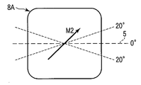
- the magnetization direction (magnetization direction) of the magnetization M ⁇ b> 2 of the magnetic pinned layer 3 is larger than 20 ° with respect to the uniaxial magnetic anisotropy direction 5 of the magnetic free layer 1. Is preferred.
- a current (current having a current density larger than the oscillation threshold current density) I between the pair of electrodes 4 is larger than the oscillation threshold current (current having the oscillation threshold current density) Ic. Is caused to generate magnetization oscillation of the magnetic free layer 1.
- the magnetic oscillation element has an oscillation frequency shift amount caused by a demagnetizing field due to magnetization vibration of the magnetic free layer 1 and an oscillation frequency shift amount caused by a magnetic field due to uniaxial magnetic anisotropy of the magnetic free layer 1 An external magnetic field acting in a direction to cancel out is given.
- the spectral oscillation line width ⁇ f becomes very narrow, and the value of the oscillation frequency can be stabilized.
- the angle ⁇ between the magnetization direction that is the center of the magnetization vibration of the magnetic free layer 1 and the magnetization direction M2 of the magnetic pinned layer 3 is in the range of 0 ° ⁇ ⁇ ⁇ 70 ° and 110 ° ⁇ ⁇ ⁇ 180 °.
- FIG. 11 shows a magnetic oscillation element according to the third embodiment.
- a feature of the magnetic oscillation element according to the third embodiment is that a constant voltage source 9 is connected between the pair of electrodes 4. About another point, it is the same as 1st embodiment.
- the magnetic oscillation element according to the example of the present invention is combined with a semiconductor device to form a composite device, the magnetic oscillation element is preferably driven at a constant voltage.
- the element resistance R varies depending on the relative angle ⁇ between the magnetization M1 of the magnetic free layer 1 and the magnetization M2 of the magnetic pinned layer 3.
- the element resistance R typically has an angle dependency as shown in the following equation.
- R R0 + ⁇ R (1-cos2 ( ⁇ / 2)) (3)
- FIG. 12 is a plot of equation (3).
- one of the objects of the present invention is to reduce the current density of the current flowing through the magnetic oscillation element, so that the magnetization oscillation of the magnetization M1 of the magnetic free layer 1 is excited with a smaller constant voltage V. Therefore, ⁇ is preferably as small as possible.
- the magnetic oscillation element has an oscillation frequency shift amount caused by a demagnetizing field due to magnetization vibration of the magnetic free layer 1 and an oscillation frequency shift amount caused by a magnetic field due to uniaxial magnetic anisotropy of the magnetic free layer 1.
- An external magnetic field acting in a direction to cancel out is given.
- the spectral oscillation line width ⁇ f becomes very narrow, and the value of the oscillation frequency can be stabilized.
- the angle ⁇ between the magnetization direction that is the center of the magnetization vibration of the magnetic free layer 1 and the magnetization direction M2 of the magnetic pinned layer 3 is in the range of 0 ° ⁇ ⁇ ⁇ 70 ° and 110 ° ⁇ ⁇ ⁇ 180 °.
- FIG. 13 shows an oscillator as a system having a magnetic oscillation element.
- the high frequency signal is input to the delay detection circuit 12 via the high pass filter 11.
- the high pass filter 11 removes noise other than the high frequency signal.
- the high-frequency signal is divided into two, one is directly input to the mixer 14, and the other is input to the mixer 14 via the delay circuit 13.
- the mixer 14 multiplies these two high-frequency signals and generates a voltage having a constant frequency.
- the low pass filter 15 removes noise other than the constant frequency voltage generated by the mixer 14.
- the high-frequency signal generation circuit 16 generates a high-frequency signal (for example, a clock signal for controlling a semiconductor device) based on a voltage having a constant frequency.
- a high-frequency signal can be extracted from the magnetic oscillation element 10 at high speed.
- a high frequency signal may be generated using a system other than this.
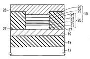
- the insulating layer 18 made of, for example, SiO 2 is formed on the semiconductor substrate 17 by the CVD method. Further, the lower electrode 19 formed of, for example, a Ta / Cu / Ta laminated structure is formed on the insulating layer 18 by sputtering.
- the magnetic oscillation element 10 is formed on the lower electrode 19.
- the magnetic oscillation element (magnetoresistance effect element) 10 is formed by forming a laminated structure of a ferromagnetic layer 20, a nonmagnetic layer 25 and a ferromagnetic layer 26 on the lower electrode 19.
- the ferromagnetic layer 20 becomes a magnetic pinned layer, and the ferromagnetic layer 26 becomes a magnetic free layer.
- the magnetic oscillation element is made to be a top pin type, the ferromagnetic layer 20 becomes a magnetic free layer and the ferromagnetic layer 26 becomes a magnetic pinned layer.
- the ferromagnetic layer 20 has a laminated structure of, for example, an antiferromagnetic layer 21 / ferromagnetic layer 22 / nonmagnetic layer 23 / ferromagnetic layer 24.
- the antiferromagnetic layer 21 is made of, for example, IrMn.
- the ferromagnetic layer 22, the nonmagnetic layer 23, and the ferromagnetic layer 24 have, for example, a SAF (synthetic anti-ferromagnetic) structure in which two ferromagnetic layers are magnetically exchange coupled.
- the ferromagnetic layer 22 is made of, for example, CoFe
- the nonmagnetic layer 23 is made of, for example, Ru
- the ferromagnetic layer 24 is made of, for example, CoFeB.
- the nonmagnetic layer 25 becomes a tunnel barrier layer and is made of, for example, MgO.
- the laminated structure of the ferromagnetic layer 20, the nonmagnetic layer 25, and the ferromagnetic layer 26 is patterned by photolithography and RIE. As a result, for example, the magnetic oscillation element 10 having an elliptical planar shape is formed.
- the insulating layer 27 is made of, for example, SiO 2 .
- the upper electrode 28 composed of, for example, a stacked structure of Au / Cu is formed on the magnetic oscillation element 10 by sputtering.
- the inventors applied a constant voltage between the lower electrode 19 and the upper electrode 28 to generate a direct current. As a result, a ferromagnetic layer (CoFeB as a magnetic free layer) was obtained. ) It was confirmed that precession occurred in the magnetization of 26).
- planar shape (size) of the magnetic oscillation element 10 is an ellipse of 60 nm (short axis) ⁇ 120 nm (long axis).
- the uniaxial magnetic anisotropy of the ferromagnetic layer 26 was imparted by shape magnetic anisotropy, and the major axis direction was the easy magnetization axis and the minor axis direction was the hard magnetization axis.
- the magnetic field generated by uniaxial magnetic anisotropy was about 250 Oe.
- the element resistance R of the magnetic oscillation element 10 was about 48 ⁇ , and the MR ratio was about 6.8%.
- the magnetic oscillation element according to the example of the present invention is composed of a magnetoresistance effect element.
- the manufacturing process of the magnetic oscillation element and the manufacturing process of the semiconductor integrated circuit are shared. It is effective to reduce the manufacturing cost.
- a spin-injection magnetic random access memory using a magnetoresistive element as a memory cell is known as a next-generation memory.
- a spin-injection magnetic random access memory is characterized in that magnetization reversal (writing) is performed by spin torque.
- the magnetic oscillation element in the oscillator 32 can be formed simultaneously with the memory cell (magnetoresistance effect element) in the memory cell array 31.
- the clock signal (reference clock) generated by the oscillator 32 composed of the magnetic oscillation element is supplied to the control circuit 33, the word line driver 34, the bit line driver / sinker 35, and the read circuit 36.
- the example of the present invention is not limited to the above-described embodiment, and can be embodied by modifying each component without departing from the scope of the invention.
- Various inventions can be configured by appropriately combining a plurality of constituent elements disclosed in the above-described embodiments. For example, some constituent elements may be deleted from all the constituent elements disclosed in the above-described embodiments, or constituent elements of different embodiments may be appropriately combined.
- the present invention relates to a reference clock in a portable electronic device, a reference clock in a single transceiver circuit chip, a local oscillator for a single chip RF spectrum analyzer, a transceiver for wireless communication, a high-frequency assist recording element, a magnetic sensor, etc.
- Industrial benefits are tremendous.
Landscapes
- Hall/Mr Elements (AREA)
- Mram Or Spin Memory Techniques (AREA)
Abstract
本発明の磁性発振素子は、磁化方向が可変の磁気フリー層(1)と、磁化方向が不変の磁気ピンド層(3)と、両者間に配置されるスペーサー層(2)と、磁気フリー層(1)に外部磁場を与える磁場発生部(7)とを備える。磁気フリー層(1)は、一軸磁気異方性を有し、それに発振閾値電流よりも大きな電流が流れることにより磁化振動を行う。磁場発生部(7)は、磁化振動による反磁場に起因する発振周波数のシフト量と磁気フリー層(1)の一軸磁気異方性による磁場に起因する発振周波数のシフト量とを相殺する方向に外部磁場の大きさ及び方向を制御する。磁気フリー層(1)の磁化振動の中心となる方向と磁気ピンド層(3)の磁化方向とのなす角度θは、0°≦θ≦70°及び110°≦θ≦180°の範囲内にある。
Description
本発明は、マイクロ波発振器に関する。
GMR素子やTMR素子といった磁気抵抗効果素子(MR素子)に、ある閾値電流ICよりも大きな直流電流Iを通電することにより、MR素子内のフリー層磁化にスピントルクが作用し、数~数十GHzの定常な磁化振動が励起されることが知られている(例えば、非特許文献1,2を参照)。
この磁化振動は、MR効果により、高周波電力に変換される。この現象が見られる典型的な素子サイズは100nm×100nm程度である。
この素子は、マイクロ波の起源が磁気的な発振に由来していることから、磁性発振素子と呼ばれる。あるいは、磁化振動の起源がスピントルクであることから、スピントルク発振器(Spin-Torque Oscillator)とも呼ばれる。
磁性発振素子の用途として、微小サイズの発振器であることを活かした用途が考案されている。その一つは、磁性発振素子を携帯用電子機器におけるリファレンスクロックとして用いるというものである。
従来の水晶発振器を磁性発振素子に置き換えれば、リファレンスクロックのスペースを小さくできるだけでなく、単一の送受信回路チップ内にリファレンスクロックを集積することが可能になる。また、RFスペクトラム解析が単一チップで行なえるようにヘテロダイン検波器内の局部発振器としての用途もある。
磁性発振素子は、磁化振動に由来する振動磁場発生器でもあるため、その振動磁場を活かす用途も考案されている。その一つは、無線通信に関するもので、磁性発振素子をコンピューター内の個々のコンポーネント間のデータ転送を担う無線通信用送信機として応用するという用途である。
磁気記録再生装置に関するものとして、例えば、特許文献1に開示されているように、アシスト記録用振動磁場発生器としての用途もある。
磁性発振素子における磁化振動は、外部からの磁場に応答するという特性を有することを活かした用途も考案されている。無線通信に関するものでは、無線通信用受信機として応用するという用途である。
さらに、磁気記録再生装置に関するものとして、例えば、特許文献2,3に開示されているように、磁気記録再生装置の再生ヘッドとしての用途が考案されている。
上記のさまざまな用途に向けた磁性発振素子に要求される主な特性として、素子から高周波出力が効率よく取り出されること、μWオーダーの高出力であること、発振周波数が安定であること、といった3要素が挙げられる。
発振周波数が安定であることが望ましいというのは、局部発振器としての用途や無線通信用送受信機としての用途を考慮してみれば、明らかなことである。周波数がふらついていては、リファレンスとしての役割は無理であるし、無線通信情報を周波数にのせようにも情報が乱されてしまう。
磁性発振素子から効率よく高周波が取り出されるためには、素子抵抗が100Ω程度であることが望まれる。これは、多くの高周波デバイスの特性インピーダンスが50Ω程度で設計され、規格化されているため、高周波デバイスとしての磁性発振素子もまたそうした規格に合わせる必要があるからである。
磁性発振素子において、磁化振動が励起される典型的な素子サイズは100nm×100nm程度であるから、磁性発振素子のRA(素子抵抗と接合面積との積)として、1Ω・μm2以下であることが要求される。
RAが1Ω・μm2以下という要求は、通常GMR素子では、容易に満足される。TMR素子では、従来は不可能であったが、近年では、スペーサー層を2~3原子分程度の膜厚で成膜する技術が進展し、RAを1Ω・μm2以下にすることが可能である。
一方、磁性発振素子から、μWオーダーの高出力を得るためには、高周波出力の起源であるMR効果を高める、すなわち、その指標であるMR比を高めることが必須である。
MR比の高い素子として、近年、MgOバリアを有する磁気トンネル接合膜が注目されている。いわゆる、MgO-MTJである。MgO-MTJは、数百%程度ものMR比を有し、実際、MgO-MTJにおける磁化振動から、数百nW程度の出力が取り出されることが良く知られている。
しかしながら、MgOは、絶縁体であるため、素子の絶縁破壊の問題がある。素子が絶縁破壊をほとんど起こすことなく高寿命であるためには、素子へ印加される電圧が、約0.1V以下であることが望まれる。
上記2つの要求から、素子に通電する電流の電流密度Jは、1.0×10⁷A/cm2(=0.1V÷1Ω・μm2)よりも小さくしなければならない。即ち、J<1.0×107A/cm2が満たされれば、素子から高周波出力が効率よく取り出されること、μWオーダーの高出力であること、という2要素は、従来技術を活かして解決することができる。
しかしながら、発振周波数が安定であること、という最後の一つの要素を満たすような磁性発振素子は未だ開示されていない。すなわち、上述の3要素のすべてを満たす磁性発振素子、具体的には、J<1.0×10⁷A/cm2であり、かつ、発振周波数が安定である磁性発振素子の開発が求められている。
S. I. Kiselev et al., Nature 425, 380 (2003)
W. H. Rippard et al., Physical Review Letters 92, 027201 (2004)
NONLINEAR PHENOMENA AND CHAOS IN MAGNETIC MATERIALS (world Scientific Publishing Co. Pte. Ltd., 1994), ISBN 981-02-1005-1
本発明は、高出力及び長寿命であり、発振周波数が安定な磁性発振素子を提案する。
本発明の例に係わる磁性発振素子は、磁化方向が可変の磁気フリー層と、磁化方向が不変の磁気ピンド層と、前記磁気フリー層及び前記磁気ピンド層間に配置されるスペーサー層と、前記磁気フリー層に外部磁場を与える磁場発生部とを備える。前記磁気フリー層及び前記磁気ピンド層は、磁化方向がそれらと前記スペーサー層との接合面に対して平行である。前記磁気フリー層は、一軸磁気異方性を有し、それに発振閾値電流よりも大きな電流が流れることにより磁化振動を行う。前記磁場発生部は、前記磁化振動による反磁場に起因する発振周波数のシフト量と前記一軸磁気異方性による磁場に起因する前記発振周波数のシフト量とを相殺する方向に前記外部磁場の大きさ及び方向を制御する。前記磁気フリー層の磁化振動の中心となる方向と前記磁気ピンド層の磁化方向とのなす角度θは、0°≦θ≦70°及び110°≦θ≦180°の範囲内にある。
本発明によれば、高出力及び長寿命であり、発振周波数が安定な磁性発振素子を実現できる。
以下、図面を参照しながら、本発明の例を実施するための最良の形態について詳細に説明する。
1. 基本構成
まず、磁性発振素子は、磁気抵抗効果素子から構成されるものとし、かつ、磁気抵抗効果素子の磁気フリー層及び磁気ピンド層は、それぞれ面内磁化(in-plane magnetization)を有するものとする。
まず、磁性発振素子は、磁気抵抗効果素子から構成されるものとし、かつ、磁気抵抗効果素子の磁気フリー層及び磁気ピンド層は、それぞれ面内磁化(in-plane magnetization)を有するものとする。
磁気フリー層に関して、面内磁化とは、磁化方向が磁気フリー層とスペーサー層との接合面に対して平行であることを意味し、磁気ピンド層に関して、面内磁化とは、磁化方向が磁気ピンド層とスペーサー層との接合面に対して平行であることを意味する。
そして、本発明の例に係わる磁性発振素子は、磁気抵抗効果素子にある電流を流したときに磁化振動が発生する現象を利用する。この磁化振動の周波数は、磁性発振素子の発振周波数となる。ある電流とは、発振閾値電流密度よりも大きな電流密度を有する電流のことである。
本発明の例では、まず、発振時に、磁気フリー層の磁化振動による反磁場に起因する発振周波数のシフト量と磁気フリー層の一軸磁気異方性による磁場に起因する発振周波数のシフト量とを相殺する方向に作用する外部磁場を、磁性発振素子に与える。
これにより、発振周波数の安定性を向上させることができる。具体的には、発振周波数の安定性の指標であるスペクトル発振線幅Δfを非常に狭くすることができる。
また、本発明の例では、磁気フリー層の磁化振動の中心となる磁化方向と磁気ピンド層の磁化方向とのなす角度θを、0°≦θ≦70°及び110°≦θ≦180°の範囲内に設定する。
0°≦θ≦70°の範囲での発振は、磁気フリー層と磁気ピンド層の磁化方向が平行となる発振(平行発振)であり、110°≦θ≦180°の範囲での発振は、磁気フリー層と磁気ピンド層の磁化方向が反平行となる発振(反平行発振)である。
磁化方向が平行とは、磁気フリー層の発振中心磁化方向と磁気ピンド層の磁化方向とのなす角度θが0°≦θ≦90°の範囲にあることを意味し、磁化方向が反平行とは、磁気フリー層の発振中心磁化方向と磁気ピンド層の磁化方向とのなす角度θが90°≦θ≦180°の範囲にあることを意味する。
これにより、1.0×10⁷A/cm2よりも小さい電流密度で磁気フリー層の磁化振動を励起することが可能になるため、高出力及び長寿命の磁性発振素子とすることができる。
また、スペーサー層をMgOから構成すれば、さらに高出力の高周波出力が得られる。
2. 実施形態
(1) 第一実施形態
図1及び図2は、第一実施形態に係る磁性発振素子を示している。
図1のAは、鳥瞰図、図1のBは、断面図、図1のCは、投射図を表している。図2は、磁性発振素子と磁場発生部との位置関係の例を表している。
(1) 第一実施形態
図1及び図2は、第一実施形態に係る磁性発振素子を示している。
図1のAは、鳥瞰図、図1のBは、断面図、図1のCは、投射図を表している。図2は、磁性発振素子と磁場発生部との位置関係の例を表している。
磁性発振素子は、磁気フリー層1と、スペーサー層2と、磁気ピンド層3と、一対の電極4とから構成される。磁気フリー層1は、強磁性体から構成され、スペーサー層2は、非磁性層(例えば、MgO)から構成される。
磁気フリー層1は、面内磁化、かつ、一軸磁気異方性を有する。磁気フリー層1の一軸磁気異方性の方向5は、図1のA及びCに図示している。
一軸磁気異方性は、結晶磁気異方性の高い材料を一様磁場内で成膜することにより、又は、成膜後に一様磁場内でアニールすることにより発生させることができる。これを結晶磁気異方性と呼ぶ。また、一軸磁気異方性は、強磁性体の形状を長方形又は楕円形にすることにより発生させることもできる。これを形状磁気異方性と呼ぶ。
磁気フリー層1の平面形状は、例えば、磁気フリー層1の一軸磁気異方性の方向5を長軸とする楕円形である。磁気ピンド層3の平面形状は、磁気フリー層1の平面形状と同じであっても、異なっていてもよい。
ここで、磁気フリー層1の平面形状とは、磁気フリー層1とスペーサー層2との接合面に平行な平面内での磁気フリー層1の形状のことを意味する。また、磁気ピンド層3の平面形状とは、磁気ピンド層3とスペーサー層2との接合面に平行な平面内での磁気ピンド層3の形状のことを意味する。
この磁性発振素子においては、一対の電極4間に、発振閾値電流(発振閾値電流密度を持つ電流)Icよりも大きな電流(発振閾値電流密度よりも大きな電流密度を持つ電流)Iを流すことにより、磁気フリー層1の磁化振動が発生する。
また、この時、磁場発生部7から磁性発振素子に、磁気フリー層1の磁化振動における反磁場に起因する発振周波数のシフト量と磁気フリー層1の一軸磁気異方性による磁場に起因する発振周波数のシフト量とを相殺する方向に作用する外部磁場を与える。
その結果、スペクトル発振線幅Δfが非常に狭くなり、発振周波数の値を安定させることができる。
また、磁気フリー層1の磁化方向(可変)M1に関し、磁気フリー層1の磁化振動の中心となる磁化方向6と磁気ピンド層3の磁化方向(不変)M2とのなす角度θを、0°≦θ≦70°及び110°≦θ≦180°の範囲内に設定する。
これにより、1.0×10⁷A/cm2よりも小さい電流密度で磁気フリー層の磁化振動を励起することが可能になるため、高出力及び長寿命の磁性発振素子とすることができる。
ここで、発振周波数の安定性について説明する。
発振周波数の安定性の指標であるスペクトル発振線幅Δfは、レーザー、電気回路発振器などの従来型の発振器と同様に次式で表すことができる。

但し、Δfresは、共振器線幅、kBTは、熱エネルギー、Eosciは、磁化振動エネルギーである。また、δは、周波数シフト効果の大きさ、及び、シフトの正負を表す因子である。δの正負の定義に依るが、例えば、δ>0であれば、周波数減少(レッドシフト)、δ<0であれば、周波数増大(ブルーシフト)を意味する。
以下、δの正負に関しては、この定義に従うことにする。
式(1)は、周波数シフト効果|δ|が大きいと、発振線幅Δfが大きくなることを示している。即ち、周波数シフト効果|δ|が大きいと、周波数安定性が悪くなることを意味している。従って、周波数が安定となるための最も理想的な状況は、δ=0である。
周波数シフト効果の大きさδは、上述のように発振線幅Δfを増大させることから、特に半導体レーザーや量子ドットレーザーなどのようなレーザー技術分野においては、線幅増大因子(linewidth enhancement factor)と呼ばれている。
さて、面内磁化フリー層(面内磁化を有する磁気フリー層)のような薄膜強磁性体において、磁化がほぼ面内にある場合、その磁化に対する反磁場による発振周波数のシフト効果は、発振周波数を減少させるレッドシフト効果であることが従来から知られている(例えば、非特許文献3を参照)。
一方、本発明者らの研究によれば、磁気フリー層に一軸磁気異方性を持たせた場合、磁化に対する一軸磁気異方性による発振周波数のシフト効果が現れる。
特に、図3に示すように、磁気フリー層の磁化M1の磁化振動の中心となる方向6が磁気フリー層1の有する一軸磁気異方性の方向5に対して45°よりも大きいときは、一軸磁気異方性による発振周波数のシフト効果が周波数を増大させるブルーシフト効果になるということが、本発明者らの研究によって明らかになっている。
従って、このような場合には、反磁場に起因するレッドシフト効果(δ>0)と、一軸磁気異方性による磁場に起因するブルーシフト効果(δ<0)が共存することになる。
そこで、レッドシフト効果とブルーシフト効果とが互いに相殺するように面内磁化フリー層の磁化M1の磁化振動の中心となる方向6を外部磁場によって制御することで、δ=0が実現され、発振線幅Δfが狭くなり、安定な周波数(磁化振動)を得ることができる。
図4は、磁化振動による反磁場に起因する発振周波数のシフト量(レッドシフト効果)と一軸磁気異方性による磁場に起因する発振周波数のシフト量(ブルーシフト効果)とが相殺する(δ=0)外部磁場の大きさをシミュレーションした結果を示している。
図5及び図6は、図4のシミュレーション結果を得るための条件を示している。
図5の場合、磁気フリー層1の磁化M1の磁化振動の中心となる方向6は、磁気フリー層1の有する一軸磁気異方性の方向5に対して垂直(90°)であり、一軸磁気異方性の方向5に対して45°よりも大きい。外部磁場Hextの方向は、磁気フリー層1の磁化M1の磁化振動の中心となる方向6に平行である。
これに対し、図6の場合、磁気フリー層1の磁化M1の磁化振動の中心となる方向6は、磁気フリー層1の有する一軸磁気異方性の方向5に対して平行(0°)であり、一軸磁気異方性の方向5に対して45°よりも小さい。外部磁場Hextの方向は、磁気フリー層1の磁化M1の磁化振動の中心となる方向6に平行である。
このシミュレーションは、磁気デバイス研究においてしばしば用いられるランダウ・リフシッツ・ギルバート(Landau-Lifshitz-Gilbert)方程式をベースにしている。
シミュレーションでは、反磁場4πMSの大きさとして、典型値である10000 [Oe]、一軸磁気異方性の磁場の大きさとして、典型値である100 [Oe]を用いている。また、ギルバートダンピングαは、0.02とした。
図4において、曲線10は、図5の条件でのシミュレーション結果であり、外部磁場Hext=380 [Oe]で、δ=0となり、磁化振動による反磁場に起因する発振周波数のシフト量(レッドシフト効果)と一軸磁気異方性による磁場に起因する発振周波数のシフト量(ブルーシフト効果)とが相殺することになる。
しかしながら、図4において、図6の条件で得られる曲線11は、外部磁場Hextに対して、常に、δ>0である。
これらの振る舞いの相違は、磁気フリー層1の磁化M1の磁化振動の中心となる方向6が、磁気フリー層1の有する一軸磁気異方性の方向5に対して45°よりも大きいか、又は、小さいか、に依存する。この45°という角度が境界値となる理由は、磁気フリー層1の磁化M1に対する一軸磁気異方性に起因する磁場の向きの正負が、その角度において反転するためである。
以上をまとめると、まず、発振周波数の安定性については、磁気フリー層1の磁化振動における反磁場に起因する発振周波数のシフト量と磁気フリー層1の一軸磁気異方性による磁場に起因する発振周波数のシフト量とを相殺する方向に外部磁場Hextを発生させることにより実現される。
特に、磁気フリー層1の磁化M1の磁化振動の中心となる方向6を、磁気フリー層1の有する一軸磁気異方性の方向5に対して45°よりも大きくすれば、δ=0とすることができ、発振周波数の安定性を向上できる。
次に、低電流密度による高出力及び長寿命について説明する。
これらの効果は、磁気フリー層の磁化振動の中心となる方向と磁気ピンド層の磁化方向とのなす角度θを、0°≦θ≦70°及び110°≦θ≦180°の範囲内にし、磁性発振素子に通電する電流の電流密度Jを1.0×10⁷A/cm2よりも小さくすることにより実現される。
図7及び図8は、発振閾値電流密度と、磁気フリー層の磁化振動の中心となる方向と磁気ピンド層の磁化方向とのなす角度θとの関係を示している。
この関係は、ランダウ・リフシッツ・ギルバート・スロンチェスキー(Landau-Lifshitz-Gilbert-Slonczewski)方程式によるシミュレーション結果である。磁気フリー層の厚さ(磁気フリー層とスペーサー層の接合面に垂直な方向における磁気フリー層の幅)dは、2nm、飽和磁化MSは、600 emu/cm3、スピン偏極率Pは、0.3、外部磁場の大きさHextは、0.08×4πMS、一軸磁気異方性による磁場の大きさHkは、0.02×4πMSとした。
図7のシミュレーションは、磁気フリー層と磁気ピンド層の磁化方向が平行となる発振(平行発振)に関する。その結果によれば、0°≦θ≦90°の範囲内では、θが大きいほど、発振閾値電流密度が増大する。本発明の目的の一つは、磁性発振素子に通電する電流の電流密度、即ち、発振閾値電流密度Jを1.0×10⁷A/cm2よりも小さくすることにある。従って、そのためには、0°≦θ≦70°とすればよいことがわかる。
また、図8のシミュレーションは、磁気フリー層と磁気ピンド層の磁化方向が反平行となる発振(反平行発振)に関する。その結果によれば、90°≦θ≦180°の範囲内では、θが小さいほど、発振閾値電流密度が増大する。また、θをθ’(=180-θ)に置き換えると、0°≦θ’≦90°の範囲内では、図7と同様に、θ’が大きいほど、発振閾値電流密度が増大する。従って、0°≦θ’≦70°とすれば、発振閾値電流密度Jを1.0×10⁷A/cm2よりも小さくすることができる。0°≦θ’≦70°は、110°≦θ≦180°と等価である。
θ=90°において、発振閾値電流密度が非常に大きくなるという物理的な理由は、磁気フリー層の磁化M1の磁化振動を励起する原因がスピントルクにある、という点にある。磁化M1に作用するスピントルクは、次式で表される。
aJ・M1 × (M1×M2) …(2)
但し、×は、ベクトル積であり、aJは、磁気フリー層に通電する電流に比例する実数である。(2)式は、面内磁化フリー層の磁化M1、面内磁化ピンド層の磁化M2に対しcosθに比例するため、θ≒90°のときに極々小さくなるような量である。そのため、θ≒90°の場合には、aJ、即ち、磁気フリー層に通電する電流の電流密度を非常に大きくしないと、磁気フリー層の磁化M1の磁化振動を励起するようなスピントルクを発生させることができない。
aJ・M1 × (M1×M2) …(2)
但し、×は、ベクトル積であり、aJは、磁気フリー層に通電する電流に比例する実数である。(2)式は、面内磁化フリー層の磁化M1、面内磁化ピンド層の磁化M2に対しcosθに比例するため、θ≒90°のときに極々小さくなるような量である。そのため、θ≒90°の場合には、aJ、即ち、磁気フリー層に通電する電流の電流密度を非常に大きくしないと、磁気フリー層の磁化M1の磁化振動を励起するようなスピントルクを発生させることができない。
以上、説明したように、本発明の第一実施形態に係る磁性発振素子においては、まず、磁気フリー層の磁化振動による反磁場に起因する発振周波数のシフト量と磁気フリー層の一軸磁気異方性による磁場に起因する発振周波数のシフト量とを相殺する方向に外部磁場を発生させることにより、発振周波数の安定性を向上させることができる。
また、これに加えて、さらに、磁気フリー層の磁化の磁化振動の中心となる方向を、磁気フリー層の有する一軸磁気異方性の方向に対して45°よりも大きくすることにより、δ=0とし、発振周波数の安定性をさらに向上させることができる。
さらに、磁気フリー層の磁化振動の中心となる磁化方向と磁気ピンド層の磁化方向とのなす角度θを、0°≦θ≦70°及び110°≦θ≦180°の範囲内に設定することにより、1.0×10⁷A/cm2よりも小さい電流密度で磁気フリー層の磁化振動を励起することができ、高出力及び長寿命の磁性発振素子とすることができる。
また、スペーサー層をMgOから構成すれば、さらに高出力の高周波出力が得られる。
(2) 第二実施形態
図9は、第二実施形態に係わる磁性発振素子を示している。
図9は、第二実施形態に係わる磁性発振素子を示している。
第二実施形態に係わる磁性発振素子の特徴は、磁気ピンド層3の構造にある。その他の点については、第一実施形態と同じである。
磁性発振素子は、磁気フリー層1と、スペーサー層2と、磁気ピンド層3と、一対の電極4とから構成される。磁気フリー層1は、強磁性体から構成され、スペーサー層2は、非磁性層(例えば、MgO)から構成される。
磁気フリー層1は、面内磁化、かつ、一軸磁気異方性を有する。磁気フリー層1の一軸磁気異方性の方向5は、図10に図示している。
磁気ピンド層3は、強磁性層8Aと反強磁性層(例えば、IrMn)8Bの積層構造から構成される。反強磁性層8Bは、強磁性層8Aとの交換結合により、強磁性層8Aの磁化方向、即ち、磁気ピンド層3の磁化方向を固定する。
ここで、図10に示すように、磁気ピンド層3の磁化M2の磁化方向(着磁方向)は、磁気フリー層1の有する一軸磁気異方性の方向5に対して20°よりも大きいことが好ましい。
なぜなら、このようにすることで、磁気フリー層1の磁化振動の中心となる磁化方向と磁気ピンド層3の磁化方向M2とのなす角度を、平行発振の場合には小さく、反平行発振の場合には大きくし易くなるためである。
第二実施形態の磁性発振素子においても、一対の電極4間に、発振閾値電流(発振閾値電流密度を持つ電流)Icよりも大きな電流(発振閾値電流密度よりも大きな電流密度を持つ電流)Iを流すことにより、磁気フリー層1の磁化振動が発生する。
また、この時、磁性発振素子に、磁気フリー層1の磁化振動による反磁場に起因する発振周波数のシフト量と磁気フリー層1の一軸磁気異方性による磁場に起因する発振周波数のシフト量とを相殺する方向に作用する外部磁場を与える。
その結果、スペクトル発振線幅Δfが非常に狭くなり、発振周波数の値を安定させることができる。
また、磁気フリー層1の磁化の磁化振動の中心となる方向を、磁気フリー層1の有する一軸磁気異方性の方向5に対して45°よりも大きくすることにより、δ=0とし、発振周波数の安定性をさらに向上させることができる。
さらに、磁気フリー層1の磁化振動の中心となる磁化方向と磁気ピンド層3の磁化方向M2とのなす角度θを、0°≦θ≦70°及び110°≦θ≦180°の範囲内に設定することにより、1.0×10⁷A/cm2よりも小さい電流密度で磁気フリー層の磁化振動を励起させ、高出力及び長寿命の磁性発振素子を実現できる。
(3) 第三実施形態
図11は、第三実施形態に係わる磁性発振素子を示している。
図11は、第三実施形態に係わる磁性発振素子を示している。
第三実施形態に係わる磁性発振素子の特徴は、一対の電極4間に定電圧源9を接続したことにある。その他の点については、第一実施形態と同じである。
半導体デバイスにおいては、電圧駆動が主流である。そのため、本発明の例に係わる磁性発振素子が半導体デバイスと融合して複合的なデバイスを構成する場合には、磁性発振素子を定電圧駆動することが好ましい。
本発明の例に係わる磁性発振素子は、磁気抵抗効果素子から構成されるため、磁気フリー層1の磁化M1と磁気ピンド層3の磁化M2との相対角度θによって素子抵抗Rが変化する。素子抵抗Rは、典型的には、次式のような角度依存性を持つ。
R = R0+ΔR(1-cos2(θ/2)) …(3)
図12は、式(3)をプロットしたものである。
R = R0+ΔR(1-cos2(θ/2)) …(3)
図12は、式(3)をプロットしたものである。
θが大きいほど、素子抵抗Rは大きくなる。また、定電圧Vで、本発明の例に係わる磁性発振素子を駆動する場合、磁性発振素子に流れる電流Iは、オームの法則 I=V/Rにより、θが大きいほど小さくなる。
既に説明したように、本発明の目的の一つは、磁性発振素子に流す電流の電流密度を小さくすることにあるため、より小さい定電圧Vで磁気フリー層1の磁化M1の磁化振動を励起させるために、θは、なるべく小さいことが好ましい。
第三実施形態の磁性発振素子においても、一対の電極4間に、発振閾値電流(発振閾値電流密度を持つ電流)Icよりも大きな電流(発振閾値電流密度よりも大きな電流密度を持つ電流)Iを流すことにより、磁気フリー層1の磁化振動が発生する。
また、この時、磁性発振素子に、磁気フリー層1の磁化振動による反磁場に起因する発振周波数のシフト量と磁気フリー層1の一軸磁気異方性による磁場に起因する発振周波数のシフト量とを相殺する方向に作用する外部磁場を与える。
その結果、スペクトル発振線幅Δfが非常に狭くなり、発振周波数の値を安定させることができる。
また、磁気フリー層1の磁化の磁化振動の中心となる方向を、磁気フリー層1の有する一軸磁気異方性の方向に対して45°よりも大きくすることにより、δ=0とし、発振周波数の安定性をさらに向上させることができる。
さらに、磁気フリー層1の磁化振動の中心となる磁化方向と磁気ピンド層3の磁化方向M2とのなす角度θを、0°≦θ≦70°及び110°≦θ≦180°の範囲内に設定することにより、1.0×10⁷A/cm2よりも小さい電流密度で磁気フリー層の磁化振動を励起させ、高出力及び長寿命の磁性発振素子を実現できる。
3. システム例
次に、本発明の例に係わる磁性発振素子から高周波信号を取り出すシステムの例について説明する。
次に、本発明の例に係わる磁性発振素子から高周波信号を取り出すシステムの例について説明する。
図13は、磁性発振素子を有するシステムとしての発振器を示している。
磁性発振素子10に定電圧源9を接続し、磁性発振素子10に直流電流Iを流すことにより、磁気フリー層1の磁化振動が発生する。この磁化振動により、磁性発振素子10の素子抵抗Rが周期的に変化することによる磁性発振素子10からの高周波信号を、例えば、以下のシステムにより検出する。
まず、高周波信号は、ハイパスフィルター11を経由して、遅延検波回路12に入力される。ハイパスフィルター11は、高周波信号以外の雑音を除去する。
遅延検波回路12において、高周波信号は、二分され、一方は、直接、ミキサー14に入力され、他方は、遅延回路13を経由してミキサー14に入力される。ミキサー14は、これら二つの高周波信号を乗積し、一定周波数の電圧を生成する。
ローパスフィルター15は、ミキサー14によって生成された一定周波数の電圧以外の雑音を除去する。
最後に、高周波信号生成回路16は、一定周波数の電圧に基づいて、高周波信号(例えば、半導体デバイスを制御するクロック信号)を生成する。
このシステムによれば、磁性発振素子10から高速に高周波信号を取り出すことができる。但し、これ以外のシステムを用いて高周波信号を生成しても構わない。
4. 製造方法
磁性発振素子の製造方法と材料例について、図14を参照しながら説明する。
磁性発振素子の製造方法と材料例について、図14を参照しながら説明する。
まず、CVD法により、半導体基板17上に、例えば、SiO2から構成される絶縁層18を形成する。また、スパッタリング法により、絶縁層18上に、例えば、Ta/Cu/Taの積層構造から構成される下部電極19を形成する。
この後、下部電極19上に磁性発振素子10を形成する。
磁性発振素子(磁気抵抗効果素子)10は、下部電極19上に、強磁性層20、非磁性層25及び強磁性層26の積層構造を形成することにより形成される。
磁性発振素子をボトムピン型にするときは、強磁性層20は、磁気ピンド層になり、強磁性層26は、磁気フリー層になる。また、磁性発振素子をトップピン型にするときは、強磁性層20は、磁気フリー層になり、強磁性層26は、磁気ピンド層になる。
ここでは、磁性発振素子をボトムピン型にする場合について説明する。
この場合、強磁性層20は、例えば、反強磁性層21/強磁性層22/非磁性層23/強磁性層24の積層構造から構成される。
この場合、強磁性層20は、例えば、反強磁性層21/強磁性層22/非磁性層23/強磁性層24の積層構造から構成される。
反強磁性層21は、例えば、IrMnから構成される。
強磁性層22、非磁性層23及び強磁性層24は、例えば、二つの強磁性層が磁気交換結合するSAF(synthetic anti-ferromagnetic)構造を有する。強磁性層22は、例えば、CoFeから構成され、非磁性層23は、例えば、Ruから構成され、強磁性層24は、例えば、CoFeBから構成される。
非磁性層25は、トンネルバリア層となり、例えば、MgOから構成される。
そして、強磁性層20、非磁性層25及び強磁性層26の積層構造は、フォトリソグラフィーとRIEにより、パターニングされる。その結果、例えば、平面形状が楕円形の磁性発振素子10が形成される。
また、この磁性発振素子10の周囲を取り囲む絶縁層27を形成する。絶縁層27は、例えば、SiO2から構成される。
最後に、スパッタリング法により、磁性発振素子10上に、例えば、Au/Cuの積層構造から構成される上部電極28を形成する。
本発明者らは、このような磁性発振素子10において、下部電極19と上部電極28との間に定電圧を印加し、直流電流を発生させたところ、磁気フリー層としての強磁性層(CoFeB)26の磁化に歳差運動が生じることを確認した。
但し、磁性発振素子10の平面形状(サイズ)は、60nm(短軸)×120nm(長軸)の楕円形である。
また、強磁性層26の一軸磁気異方性は、形状磁気異方性により付与し、長軸方向を磁化容易軸とし、短軸方向を磁化困難軸とした。一軸磁気異方性により発生する磁場は、約250 Oeであった。
さらに、この磁性発振素子10の素子抵抗Rは、約48Ω、MR比は、約6.8%であった。
5. 適用例
本発明の例に係わる磁性発振素子は、磁気抵抗効果素子から構成される。
本発明の例に係わる磁性発振素子は、磁気抵抗効果素子から構成される。
磁性発振素子を、例えば、半導体集積回路の動作タイミングを制御するクロック信号(リファレンスクロック)を生成する発振器に使用する場合には、磁性発振素子の製造プロセスと半導体集積回路の製造プロセスとの共通化を図ることが製造コストの低下には効果的である。
ここで、次世代メモリとして、磁気抵抗効果素子をメモリセルとするスピン注入磁気ランダムアクセスメモリが知られている。
スピン注入磁気ランダムアクセスメモリは、磁化反転(書き込み)をスピントルクにより行うことに特徴を有する。
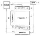
そこで、例えば、図15に示すように、本発明の例に係わる磁性発振素子を磁気ランダムアクセスメモリに適用することは非常に有効である。
なぜなら、メモリセルアレイ31内のメモリセル(磁気抵抗効果素子)と同時に発振器32内の磁性発振素子を形成することができるためである。
この場合、磁性発振素子から構成される発振器32により生成したクロック信号(リファレンスクロック)は、制御回路33、ワード線ドライバ34、ビット線ドライバ/シンカー35及び読み出し回路36に供給される。
6. むすび
本発明によれば、高出力及び長寿命であり、発振周波数が安定な磁性発振素子を実現できる。
本発明によれば、高出力及び長寿命であり、発振周波数が安定な磁性発振素子を実現できる。
本発明の例は、上述の実施形態に限定されるものではなく、その要旨を逸脱しない範囲で、各構成要素を変形して具体化できる。また、上述の実施形態に開示されている複数の構成要素の適宜な組み合せにより種々の発明を構成できる。例えば、上述の実施形態に開示される全構成要素から幾つかの構成要素を削除してもよいし、異なる実施形態の構成要素を適宜組み合わせてもよい。
本発明は、携帯用電子機器におけるリファレンスクロック、単一の送受信回路チップ内リファレンスクロック、単一チップRFスペクトラムアナライザ用局部発振器、無線通信用送受信器、高周波アシスト記録用素子、磁気センサーなどに対して、産業上のメリットは多大である。
1: 磁気フリー層、 2: スペーサー層、 3: 磁気ピンド層、 4: 電極、 5: 一軸磁気異方性の方向、 6: 磁気フリー層の磁化振動の中心となる方向、 7: 磁場発生部、 8A,20,22,24,26: 強磁性層、 8B,21: 反強磁性層、 9: 定電圧源、 10: 磁性発振素子、 11: ハイパスフィルター、 12: 遅延検波回路、 13: 遅延回路、 14: ミキサー、 15: ローパスフィルター、 16: 高周波信号生成回路、 17: 半導体基板、 18,27: 絶縁層、 19: 下部電極、 23,25: 非磁性層、 28: 上部電極、 31: メモリセルアレイ、 32: 発振器、 33: 制御回路、 34: ワード線ドライバ、 35: ビット線ドライバ/シンカー、 36: 読み出し回路。
Claims (5)
- 磁化方向が可変の磁気フリー層と、
磁化方向が不変の磁気ピンド層と、
前記磁気フリー層及び前記磁気ピンド層間に配置されるスペーサー層と、
前記磁気フリー層に外部磁場を与える磁場発生部とを具備し、
前記磁気フリー層及び前記磁気ピンド層は、磁化方向がそれらと前記スペーサー層との接合面に対して平行であり、
前記磁気フリー層は、一軸磁気異方性を有し、それに発振閾値電流よりも大きな電流が流れることにより磁化振動を行い、
前記磁場発生部は、前記磁化振動による反磁場に起因する発振周波数のシフト量と前記一軸磁気異方性による磁場に起因する前記発振周波数のシフト量とを相殺する方向に前記外部磁場の大きさ及び方向を制御し、
前記磁気フリー層の磁化振動の中心となる方向と前記磁気ピンド層の磁化方向とのなす角度θは、0°≦θ≦70°及び110°≦θ≦180°の範囲内にある
ことを特徴とする磁性発振素子。 - 前記磁気フリー層の磁化振動の中心となる方向は、前記一軸磁気異方性の方向に対して45°よりも大きいことを特徴とする請求項1に記載の磁性発振素子。
- 前記磁気ピンド層の磁化方向は、前記一軸磁気異方性の方向に対して20°よりも大きいことを特徴とする請求項1又は2に記載の磁性発振素子。
- 前記磁気フリー層の平面形状は、前記一軸磁気異方性の方向を長軸とする楕円形であることを特徴とする請求項1乃至3のいずれか1項に記載の磁性発振素子。
- 前記発振周波数は、半導体集積回路のリファレンスクロックの周波数となることを特徴とする請求項1乃至4のいずれか1項に記載の磁性発振素子。
Priority Applications (1)
| Application Number | Priority Date | Filing Date | Title |
|---|---|---|---|
| US13/216,968 US8207806B2 (en) | 2009-02-24 | 2011-08-24 | Magnetic oscillation element |
Applications Claiming Priority (2)
| Application Number | Priority Date | Filing Date | Title |
|---|---|---|---|
| JP2009041100A JP5443783B2 (ja) | 2009-02-24 | 2009-02-24 | 磁性発振素子 |
| JP2009-041100 | 2009-02-24 |
Related Child Applications (1)
| Application Number | Title | Priority Date | Filing Date |
|---|---|---|---|
| US13/216,968 Continuation US8207806B2 (en) | 2009-02-24 | 2011-08-24 | Magnetic oscillation element |
Publications (1)
| Publication Number | Publication Date |
|---|---|
| WO2010097997A1 true WO2010097997A1 (ja) | 2010-09-02 |
Family
ID=42665218
Family Applications (1)
| Application Number | Title | Priority Date | Filing Date |
|---|---|---|---|
| PCT/JP2009/070045 Ceased WO2010097997A1 (ja) | 2009-02-24 | 2009-11-27 | 磁性発振素子 |
Country Status (3)
| Country | Link |
|---|---|
| US (1) | US8207806B2 (ja) |
| JP (1) | JP5443783B2 (ja) |
| WO (1) | WO2010097997A1 (ja) |
Cited By (1)
| Publication number | Priority date | Publication date | Assignee | Title |
|---|---|---|---|---|
| WO2012056087A1 (en) | 2010-10-25 | 2012-05-03 | Nokia Corporation | An apparatus for spectrum sensing and associated methods |
Families Citing this family (6)
| Publication number | Priority date | Publication date | Assignee | Title |
|---|---|---|---|---|
| KR20120056019A (ko) * | 2010-11-24 | 2012-06-01 | 삼성전자주식회사 | 발진기와 그 제조방법 및 동작방법 |
| CN103021610B (zh) * | 2011-09-26 | 2015-12-02 | 东莞市炫耀电子有限公司 | 一种新型复合永磁材料及其制备方法 |
| JP6056630B2 (ja) * | 2013-04-18 | 2017-01-11 | Tdk株式会社 | 発振器、送信装置、整流器、整流装置、受信器、受信装置および送受信装置 |
| JP6569349B2 (ja) * | 2015-07-17 | 2019-09-04 | Tdk株式会社 | 磁気抵抗効果デバイス |
| JP6569350B2 (ja) * | 2015-07-17 | 2019-09-04 | Tdk株式会社 | 磁気抵抗効果デバイス |
| JP6323525B2 (ja) * | 2016-10-11 | 2018-05-16 | Tdk株式会社 | 整流器、整流装置、受信器および受信装置 |
Citations (2)
| Publication number | Priority date | Publication date | Assignee | Title |
|---|---|---|---|---|
| JP2008053915A (ja) * | 2006-08-23 | 2008-03-06 | Sharp Corp | マイクロ波発振素子及びその製造方法、並びに該マイクロ波発振素子を備えたマイクロ波発振装置 |
| JP2008084879A (ja) * | 2006-09-25 | 2008-04-10 | Toshiba Corp | 磁気発振素子、磁気センサ、磁気ヘッド及び磁気記録再生装置 |
Family Cites Families (6)
| Publication number | Priority date | Publication date | Assignee | Title |
|---|---|---|---|---|
| EP1548702A1 (en) * | 2003-12-24 | 2005-06-29 | Interuniversitair Microelektronica Centrum Vzw | Method for ultra-fast controlling of a magnetic cell and related devices |
| US20060039089A1 (en) * | 2004-08-17 | 2006-02-23 | Kabushiki Kaisha Toshiba | Magnetic oscillator, magnetic head, and magnetic recording and reproducing apparatus |
| JP4886268B2 (ja) * | 2005-10-28 | 2012-02-29 | 株式会社東芝 | 高周波発振素子、ならびにそれを用いた車載レーダー装置、車間通信装置および情報端末間通信装置 |
| JP2009080904A (ja) * | 2007-09-26 | 2009-04-16 | Toshiba Corp | 磁気記録装置 |
| KR101291778B1 (ko) * | 2007-12-19 | 2013-07-30 | 후지 덴키 가부시키가이샤 | 스핀 밸브 소자의 구동 방법 및 스핀 밸브 소자 |
| US7800938B2 (en) * | 2008-08-07 | 2010-09-21 | Seagate Technology, Llc | Oscillating current assisted spin torque magnetic memory |
-
2009
- 2009-02-24 JP JP2009041100A patent/JP5443783B2/ja not_active Expired - Fee Related
- 2009-11-27 WO PCT/JP2009/070045 patent/WO2010097997A1/ja not_active Ceased
-
2011
- 2011-08-24 US US13/216,968 patent/US8207806B2/en active Active
Patent Citations (2)
| Publication number | Priority date | Publication date | Assignee | Title |
|---|---|---|---|---|
| JP2008053915A (ja) * | 2006-08-23 | 2008-03-06 | Sharp Corp | マイクロ波発振素子及びその製造方法、並びに該マイクロ波発振素子を備えたマイクロ波発振装置 |
| JP2008084879A (ja) * | 2006-09-25 | 2008-04-10 | Toshiba Corp | 磁気発振素子、磁気センサ、磁気ヘッド及び磁気記録再生装置 |
Non-Patent Citations (2)
| Title |
|---|
| KUDO, K. ET AL.: "Amplitude-phase coupling in a spin-torque nano-oscillator, art 07D105", JOURNAL OF APPLIED PHYSICS, vol. 105, no. ISS.7, 3 February 2009 (2009-02-03) * |
| THADANI, K.V ET AL.: "Strong linewidth variation for spin-torque nano-oscillators as a function of in-plane magnetic field angle, art 024409", PHYSICAL REVIEW B, vol. 78, no. ISS.2, July 2008 (2008-07-01) * |
Cited By (3)
| Publication number | Priority date | Publication date | Assignee | Title |
|---|---|---|---|---|
| WO2012056087A1 (en) | 2010-10-25 | 2012-05-03 | Nokia Corporation | An apparatus for spectrum sensing and associated methods |
| US8421440B2 (en) | 2010-10-25 | 2013-04-16 | Nokia Corporation | Apparatus for spectrum sensing and associated methods |
| EP2633565A4 (en) * | 2010-10-25 | 2017-06-14 | Nokia Technologies Oy | An apparatus for spectrum sensing and associated methods |
Also Published As
| Publication number | Publication date |
|---|---|
| JP5443783B2 (ja) | 2014-03-19 |
| US8207806B2 (en) | 2012-06-26 |
| JP2010199231A (ja) | 2010-09-09 |
| US20120032763A1 (en) | 2012-02-09 |
Similar Documents
| Publication | Publication Date | Title |
|---|---|---|
| Dieny et al. | Opportunities and challenges for spintronics in the microelectronics industry | |
| JP5673951B2 (ja) | 電界強磁性共鳴励起方法及びそれを用いた磁気機能素子 | |
| TWI551035B (zh) | 具有多重固定鐵磁層或多重自由鐵磁層的自旋扭矩震盪器 | |
| JP5526141B2 (ja) | 磁性発振素子 | |
| US9966901B2 (en) | Spin-torque oscillator based on easy-cone anisotropy | |
| JP5443783B2 (ja) | 磁性発振素子 | |
| US9222994B2 (en) | Perpendicular spin torque oscillator FMR frequency measurement method | |
| JP4978553B2 (ja) | 発振デバイス、通信装置、及び磁性素子による発振方法 | |
| Miura et al. | Voltage-induced magnetization dynamics in CoFeB/MgO/CoFeB magnetic tunnel junctions | |
| JP5280516B2 (ja) | 電波分波器 | |
| JP6081591B2 (ja) | スピン波回路の動作制御方法 | |
| JP2009515406A (ja) | スピン偏極電流を利用する無線周波数発振器 | |
| JP4633689B2 (ja) | マイクロ波発振素子及びその製造方法、並びに該マイクロ波発振素子を備えたマイクロ波発振装置 | |
| CN102709465A (zh) | 具有弱交换耦合的反铁磁层的磁性器件 | |
| Mahato et al. | Tunable configurational anisotropy in collective magnetization dynamics of Ni80Fe20 nanodot arrays with varying dot shapes | |
| JP2019161176A (ja) | スピン軌道トルク型磁化回転素子、スピン軌道トルク型磁気抵抗効果素子、磁気メモリ及び発振器 | |
| CN112335063A (zh) | 单个磁性层微波振荡器 | |
| JP2019129164A (ja) | 磁気抵抗効果デバイス | |
| Gopman et al. | Large Interfacial Magnetostriction in (Co/Ni) 4/Pb (Mg1/3Nb2/3) O3–PbTiO3 Multiferroic Heterostructures | |
| Mishra et al. | Acoustically assisted energy efficient field free spin orbit torque switching of out of plane nanomagnet | |
| JP2021152521A (ja) | 磁気抵抗効果デバイスおよびセンサ | |
| Regmi | Exploring Coherent Spin Dynamics in Insulating Antiferromagnetic Systems | |
| Busel et al. | Nonlinear spin dynamics across Néel phase transition in ferromagnetic/antiferromagnetic multilayers | |
| Gayathri et al. | Thickness-induced reversal of magnetoresistance polarity in CoFeNi-based MTJs: evolution from coherent switching to vortex-state transport | |
| Stebliy et al. | Reconfiguration of a Magnetic Tunnel Junction as a Way to Turn It into a Field-Free Vortex Oscillator |
Legal Events
| Date | Code | Title | Description |
|---|---|---|---|
| 121 | Ep: the epo has been informed by wipo that ep was designated in this application |
Ref document number: 09840844 Country of ref document: EP Kind code of ref document: A1 |
|
| NENP | Non-entry into the national phase |
Ref country code: DE |
|
| 122 | Ep: pct application non-entry in european phase |
Ref document number: 09840844 Country of ref document: EP Kind code of ref document: A1 |