WO2010074074A1 - 赤外光線用透過光学部材とその製造方法、光学デバイス、及び光学装置 - Google Patents
赤外光線用透過光学部材とその製造方法、光学デバイス、及び光学装置 Download PDFInfo
- Publication number
- WO2010074074A1 WO2010074074A1 PCT/JP2009/071315 JP2009071315W WO2010074074A1 WO 2010074074 A1 WO2010074074 A1 WO 2010074074A1 JP 2009071315 W JP2009071315 W JP 2009071315W WO 2010074074 A1 WO2010074074 A1 WO 2010074074A1
- Authority
- WO
- WIPO (PCT)
- Prior art keywords
- infrared
- wavelength
- optical
- polycrystalline silicon
- optical member
- Prior art date
- Legal status (The legal status is an assumption and is not a legal conclusion. Google has not performed a legal analysis and makes no representation as to the accuracy of the status listed.)
- Ceased
Links
Images





Classifications
-
- G—PHYSICS
- G01—MEASURING; TESTING
- G01J—MEASUREMENT OF INTENSITY, VELOCITY, SPECTRAL CONTENT, POLARISATION, PHASE OR PULSE CHARACTERISTICS OF INFRARED, VISIBLE OR ULTRAVIOLET LIGHT; COLORIMETRY; RADIATION PYROMETRY
- G01J5/00—Radiation pyrometry, e.g. infrared or optical thermometry
- G01J5/02—Constructional details
- G01J5/08—Optical arrangements
-
- C—CHEMISTRY; METALLURGY
- C01—INORGANIC CHEMISTRY
- C01B—NON-METALLIC ELEMENTS; COMPOUNDS THEREOF; METALLOIDS OR COMPOUNDS THEREOF NOT COVERED BY SUBCLASS C01C
- C01B33/00—Silicon; Compounds thereof
- C01B33/02—Silicon
- C01B33/021—Preparation
- C01B33/027—Preparation by decomposition or reduction of gaseous or vaporised silicon compounds other than silica or silica-containing material
- C01B33/03—Preparation by decomposition or reduction of gaseous or vaporised silicon compounds other than silica or silica-containing material by decomposition of silicon halides or halosilanes or reduction thereof with hydrogen as the only reducing agent
-
- C—CHEMISTRY; METALLURGY
- C01—INORGANIC CHEMISTRY
- C01B—NON-METALLIC ELEMENTS; COMPOUNDS THEREOF; METALLOIDS OR COMPOUNDS THEREOF NOT COVERED BY SUBCLASS C01C
- C01B33/00—Silicon; Compounds thereof
- C01B33/02—Silicon
- C01B33/021—Preparation
- C01B33/027—Preparation by decomposition or reduction of gaseous or vaporised silicon compounds other than silica or silica-containing material
- C01B33/035—Preparation by decomposition or reduction of gaseous or vaporised silicon compounds other than silica or silica-containing material by decomposition or reduction of gaseous or vaporised silicon compounds in the presence of heated filaments of silicon, carbon or a refractory metal, e.g. tantalum or tungsten, or in the presence of heated silicon rods on which the formed silicon is deposited, a silicon rod being obtained, e.g. Siemens process
-
- G—PHYSICS
- G01—MEASURING; TESTING
- G01J—MEASUREMENT OF INTENSITY, VELOCITY, SPECTRAL CONTENT, POLARISATION, PHASE OR PULSE CHARACTERISTICS OF INFRARED, VISIBLE OR ULTRAVIOLET LIGHT; COLORIMETRY; RADIATION PYROMETRY
- G01J1/00—Photometry, e.g. photographic exposure meter
- G01J1/02—Details
- G01J1/04—Optical or mechanical part supplementary adjustable parts
-
- G—PHYSICS
- G01—MEASURING; TESTING
- G01J—MEASUREMENT OF INTENSITY, VELOCITY, SPECTRAL CONTENT, POLARISATION, PHASE OR PULSE CHARACTERISTICS OF INFRARED, VISIBLE OR ULTRAVIOLET LIGHT; COLORIMETRY; RADIATION PYROMETRY
- G01J1/00—Photometry, e.g. photographic exposure meter
- G01J1/02—Details
- G01J1/04—Optical or mechanical part supplementary adjustable parts
- G01J1/0407—Optical elements not provided otherwise, e.g. manifolds, windows, holograms, gratings
-
- G—PHYSICS
- G01—MEASURING; TESTING
- G01J—MEASUREMENT OF INTENSITY, VELOCITY, SPECTRAL CONTENT, POLARISATION, PHASE OR PULSE CHARACTERISTICS OF INFRARED, VISIBLE OR ULTRAVIOLET LIGHT; COLORIMETRY; RADIATION PYROMETRY
- G01J5/00—Radiation pyrometry, e.g. infrared or optical thermometry
- G01J5/02—Constructional details
- G01J5/04—Casings
-
- G—PHYSICS
- G01—MEASURING; TESTING
- G01J—MEASUREMENT OF INTENSITY, VELOCITY, SPECTRAL CONTENT, POLARISATION, PHASE OR PULSE CHARACTERISTICS OF INFRARED, VISIBLE OR ULTRAVIOLET LIGHT; COLORIMETRY; RADIATION PYROMETRY
- G01J5/00—Radiation pyrometry, e.g. infrared or optical thermometry
- G01J5/02—Constructional details
- G01J5/04—Casings
- G01J5/046—Materials; Selection of thermal materials
-
- G—PHYSICS
- G01—MEASURING; TESTING
- G01J—MEASUREMENT OF INTENSITY, VELOCITY, SPECTRAL CONTENT, POLARISATION, PHASE OR PULSE CHARACTERISTICS OF INFRARED, VISIBLE OR ULTRAVIOLET LIGHT; COLORIMETRY; RADIATION PYROMETRY
- G01J5/00—Radiation pyrometry, e.g. infrared or optical thermometry
- G01J5/02—Constructional details
- G01J5/08—Optical arrangements
- G01J5/0801—Means for wavelength selection or discrimination
- G01J5/0802—Optical filters
-
- G—PHYSICS
- G01—MEASURING; TESTING
- G01J—MEASUREMENT OF INTENSITY, VELOCITY, SPECTRAL CONTENT, POLARISATION, PHASE OR PULSE CHARACTERISTICS OF INFRARED, VISIBLE OR ULTRAVIOLET LIGHT; COLORIMETRY; RADIATION PYROMETRY
- G01J5/00—Radiation pyrometry, e.g. infrared or optical thermometry
- G01J5/02—Constructional details
- G01J5/08—Optical arrangements
- G01J5/0853—Optical arrangements having infrared absorbers other than the usual absorber layers deposited on infrared detectors like bolometers, wherein the heat propagation between the absorber and the detecting element occurs within a solid
-
- G—PHYSICS
- G01—MEASURING; TESTING
- G01J—MEASUREMENT OF INTENSITY, VELOCITY, SPECTRAL CONTENT, POLARISATION, PHASE OR PULSE CHARACTERISTICS OF INFRARED, VISIBLE OR ULTRAVIOLET LIGHT; COLORIMETRY; RADIATION PYROMETRY
- G01J5/00—Radiation pyrometry, e.g. infrared or optical thermometry
- G01J5/02—Constructional details
- G01J5/08—Optical arrangements
- G01J5/0875—Windows; Arrangements for fastening thereof
-
- G—PHYSICS
- G02—OPTICS
- G02B—OPTICAL ELEMENTS, SYSTEMS OR APPARATUS
- G02B5/00—Optical elements other than lenses
- G02B5/20—Filters
- G02B5/208—Filters for use with infrared or ultraviolet radiation, e.g. for separating visible light from infrared and/or ultraviolet radiation
-
- G—PHYSICS
- G01—MEASURING; TESTING
- G01J—MEASUREMENT OF INTENSITY, VELOCITY, SPECTRAL CONTENT, POLARISATION, PHASE OR PULSE CHARACTERISTICS OF INFRARED, VISIBLE OR ULTRAVIOLET LIGHT; COLORIMETRY; RADIATION PYROMETRY
- G01J1/00—Photometry, e.g. photographic exposure meter
- G01J1/02—Details
- G01J1/04—Optical or mechanical part supplementary adjustable parts
- G01J1/0488—Optical or mechanical part supplementary adjustable parts with spectral filtering
-
- G—PHYSICS
- G01—MEASURING; TESTING
- G01J—MEASUREMENT OF INTENSITY, VELOCITY, SPECTRAL CONTENT, POLARISATION, PHASE OR PULSE CHARACTERISTICS OF INFRARED, VISIBLE OR ULTRAVIOLET LIGHT; COLORIMETRY; RADIATION PYROMETRY
- G01J5/00—Radiation pyrometry, e.g. infrared or optical thermometry
- G01J5/0022—Radiation pyrometry, e.g. infrared or optical thermometry for sensing the radiation of moving bodies
- G01J5/0025—Living bodies
Definitions
- the present invention relates to a transmission optical member for infrared light, a method for manufacturing the same, an optical device, and an optical apparatus, and more specifically, a transmission optical member for infrared light suitable for human body sensing, a method for manufacturing the same, and the infrared light transmission
- the present invention relates to an optical device such as an infrared detector that senses a human body using a transmission optical member, and an optical apparatus that blocks infrared light in a specific wavelength region using the optical device.
- Silicon materials have good transmittance over a wide range from the near infrared region to the terahertz (THz) region (wavelength: about 1.1 ⁇ m to 10 mm), are excellent in workability, and are easily available. Widely used as a material for lenses and window plates.
- THz terahertz
- Non-Patent Document 1 describes an infrared window plate having a transmission spectrum as shown in FIG.
- the infrared window plate of Non-Patent Document 1 has a good linear transmittance of about 55% in a wavelength band of 1.2 to 6 ⁇ m, and should be preferably used in such a wavelength band. It is thought that you can.
- infrared detector since the infrared wavelength corresponding to the temperature of the human body (body temperature) around 37 ° C. is about 10.6 ⁇ m, in order to sense the human body using the infrared transmission action, It is desired to have a high infrared transmittance in a wavelength band in the range of 8 to 12 ⁇ m near 10.6 ⁇ m.
- Patent Document 1 proposes an infrared optical element obtained by processing polycrystalline silicon having a purity of nine nines (9N: 99.999999999%) or higher produced by a CVD method into a lens shape or a filter shape.
- Patent Document 1 a mixed gas of high purity silicon compound such as monosilane (SiH 4 ) and hydrogen is heated to 900 to 1200 ° C. to reduce hydrogen by CVD, and thereby high purity polycrystalline silicon of 9N is obtained. Is making. An infrared optical element having an antireflection film and having a transmittance of 90% or more at a wavelength of 9 ⁇ m is obtained.
- Non-Patent Document 1 shows high transmittance in the wavelength range of 1.2 to 6 ⁇ m, but there is a large loss due to absorption when the wavelength is in the vicinity of 9 ⁇ m. Although this is considered to be due to impurity defects (oxygen), the linear transmittance in the wavelength region near 9 ⁇ m is low, so it is not suitable for an infrared detector for human body sensing.
- the middle / near infrared rays (having a wavelength of about 0.78 to 4 ⁇ m) have a higher light intensity because the wavelength is shorter than the far infrared rays of 8 to 12 ⁇ m described above. If these infrared rays in the middle / near infrared region are transmitted through the optical element, the light emitted from the human body becomes stray light, which may degrade the S / N ratio. Therefore, it is necessary to suppress the linear transmittance of infrared rays in the middle / near infrared region.
- the present inventors made trichlorosilane as a raw material and produced polycrystalline silicon by the same method as in Patent Document 1. As a result, not only in the wavelength region near 9 ⁇ m, but also in the middle / near infrared light region with a short wavelength, It was found to show a high linear transmittance. Therefore, as described above, the S / N ratio may be deteriorated and the human body may not be sensed with high sensitivity.
- the present invention has been made in view of such circumstances, and an infrared ray transmitting optical member capable of sensing a human body with high sensitivity and high accuracy, a manufacturing method thereof, and an optical device using the infrared ray transmitting optical member.
- An object of the present invention is to provide an infrared detector and an optical apparatus using the optical device.
- a transmission optical member for infrared rays according to the present invention (hereinafter simply referred to as “transmission optical member”) is made of polycrystalline silicon formed from high-purity trichlorosilane as a raw material, and has a thickness of 4 ⁇ m. It is characterized by absorbing and scattering infrared rays in the following wavelength ranges.
- absorb and scatter means that the ratio of the transmittance in the wavelength region of 4 ⁇ m or less to the transmittance in the wavelength region near 10 ⁇ m is less than 1.
- the transmission optical member of the present invention is characterized in that the ratio A / B between the infrared transmittance A at a wavelength of 4 ⁇ m and the infrared transmittance B at a wavelength of 10 ⁇ m is 0.9 or less.
- the transmission optical member of the present invention is characterized in that the polycrystalline silicon has an average crystal grain size of 5 ⁇ m or less.
- the transmission optical member of the present invention is characterized in that the polycrystalline silicon is formed using a chemical vapor deposition method.
- the method for producing a transmissive optical member according to the present invention heats a substrate incorporated in a reaction vessel to a temperature of 800 to 900 ° C., and supplies a raw material gas containing at least high-purity trichlorosilane and hydrogen to the reaction vessel. And reducing the trichlorosilane to deposit polycrystalline silicon on the substrate.
- the optical device according to the present invention is characterized in that a main part includes the above-described transmission optical member.
- optical device of the present invention is an infrared detector.
- An optical device includes first and second semiconductor lasers that emit laser light on the same optical axis, and a nonlinear optical crystal that is disposed on the optical axis and on which the laser light is incident. And filtering means for filtering light in a specific wavelength region of the laser light emitted from the nonlinear optical crystal, wherein the filtering means is composed of the optical device described above.
- the transmission optical member of the present invention is composed of polycrystalline silicon formed using high-purity trichlorosilane as a raw material, and absorbs and scatters infrared rays in a wavelength region of 4 ⁇ m or less. It is difficult for infrared rays to pass through, and human body sensing can be performed with a high S / N ratio. In addition, since it is formed of polycrystalline silicon, it can be obtained at a lower cost than single crystal silicon.
- the ratio A / B between the infrared transmittance A at a wavelength of 4 ⁇ m and the infrared transmittance B at a wavelength of 10 ⁇ m is 0.9 or less, it is 10 ⁇ m and its vicinity (hereinafter simply referred to as “near 10 ⁇ m”).
- the transmittance for infrared rays in the wavelength region is high, and the transmittance for infrared rays in the middle / near infrared region is low.
- the average crystal grain size of the polycrystalline silicon is 5 ⁇ m or less, the average crystal grain size is also minute, and the transmittance of infrared rays in the wavelength region of 4 ⁇ m or less can be suppressed.
- the polycrystalline silicon is formed by using a chemical vapor deposition method, it is possible to avoid contamination of impurities as in the CZ method (Czochralski method) and the FZ method (floating method). Polycrystalline silicon having a high purity of 10N to 11N can be easily obtained.
- the base material incorporated in the reaction vessel is heated to a temperature of 800 to 900 ° C., and the source gas containing at least high-purity trichlorosilane and hydrogen is reacted with the reaction gas. Since the trichlorosilane is supplied to a container to reduce the trichlorosilane and polycrystalline silicon is deposited on the substrate, a transmission optical material having a desired transmission spectrum can be obtained at a low cost without causing coarsening of crystal particles. Can do.
- the optical device of the present invention since the main part includes the above-described transmission optical member, the infrared ray in the wavelength region near 10 ⁇ m is suppressed while suppressing the transmittance of the infrared ray in the wavelength region of 4 ⁇ m or less. An optical device that can transmit light can be obtained.
- the optical device of the present invention is an infrared detector, the human body can be detected with high sensitivity.
- An optical device includes first and second semiconductor lasers that emit laser light on the same optical axis, and a nonlinear optical crystal that is disposed on the optical axis and on which the laser light is incident.
- Filter means for blocking light in a specific wavelength region of the laser light emitted from the nonlinear optical crystal, and the filter means is composed of the optical device described above. Only the excitation frequency of the semiconductor laser is filtered, and only the difference frequency between the oscillation frequencies of the first and second semiconductor lasers can be extracted with high efficiency.
- FIG. 1 is an apparatus configuration diagram showing an outline of an embodiment of an optical apparatus according to the present invention. It is a figure which shows the transmission spectrum of the sample of Example 1. FIG. It is a figure which shows the transmission spectrum of the sample of the comparative example 1. It is a figure which shows the transmission spectrum of the sample of the comparative example 2. FIG. It is a figure which shows the transmission spectrum of the infrared window plate described in the nonpatent literature 1.
- the transmission optical member according to the present invention is made of polycrystalline silicon using 10N to 11N high-purity trichlorosilane (SiHCl 3 ) as a raw material, and is configured to absorb and scatter infrared rays in a wavelength region of 4 ⁇ m or less. ing. As a result, a transmission optical material suitable for human body sensing can be obtained.
- the human body temperature is around 37 ° C.
- the corresponding infrared wavelength is around 10.6 ⁇ m. Therefore, in order to detect the presence of the human body by the infrared rays emitted from the human body, it is necessary that the infrared transmittance is high in a wavelength range of 8 to 12 ⁇ m centering on 10.6 ⁇ m.
- the mid-infrared region (wavelength: 2 to 4 ⁇ m) and the near-infrared region (wavelength: 0.78 to 2 ⁇ m) are shorter than the above-mentioned wavelength region of 8 to 12 ⁇ m, and the light intensity of infrared rays is low. strong. Therefore, if the infrared transmittance in the middle / near infrared region is 4 ⁇ m or less, the infrared rays in these middle / near infrared regions become the stray light of the infrared rays emitted from the human body, and the S / N ratio is reduced. May deteriorate. As a result, the human body cannot be detected with high accuracy, and the reliability of human body detection may be impaired.
- the transmission optical member of the present invention is configured so that infrared rays in a wavelength region of 4 ⁇ m or less are absorbed and scattered. That is, the transmission optical member is configured such that the ratio of the transmittance in the wavelength region of 4 ⁇ m or less to the transmittance in the wavelength region near 10 ⁇ m is less than 1.
- FIG. 1 is a diagram showing an example of a transmission spectrum of the transmission optical member.
- the horizontal axis represents wavelength ( ⁇ m), and the vertical axis represents infrared linear transmittance (%).
- the transmission optical member has a high transmittance in the wavelength region of 8 to 12 ⁇ m near 10 ⁇ m, and the transmittance decreases as the wavelength becomes shorter.
- the ratio A / B between the infrared transmittance A at a wavelength of 4 ⁇ m and the infrared transmittance B at a wavelength of 10 ⁇ m is 0.9 or less.
- infrared light in the wavelength region of 4 ⁇ m or less becomes stray light in the vicinity of 10 ⁇ m, for example, in the wavelength region of 8 to 12 ⁇ m. It can be avoided as much as possible. Thereby, a good S / N ratio can be obtained, and the human body can be sensed with high accuracy.
- the transmission spectrum becomes flat over a wide wavelength band from the mid-infrared region to the far-infrared region, so that infrared rays having a wavelength of 4 ⁇ m or less are stray light. This may make it difficult to perform highly accurate human body sensing. Therefore, it is preferable that the average crystal grain size of polycrystalline silicon is as small as possible, specifically 5 ⁇ m or less.
- the transmission optical member can be easily manufactured by a chemical vapor deposition method (CVD method) using SiHCl 3 as a raw material.
- CVD method chemical vapor deposition method
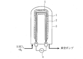
- FIG. 2 is an internal structure diagram showing an embodiment of a CVD apparatus used for manufacturing a transmissive optical member.
- a rod 2 having a predetermined diameter made of high-purity polycrystalline silicon and having a heater 1 embedded therein is mounted in a reaction vessel 3, and a heating power source 4 is connected to the heater 1. .
- the inside of the reaction vessel 3 is sucked with a vacuum pump to reduce the pressure, and the heating power source 4 is turned on to raise the temperature of the heater 1 to 800 to 900 ° C. to heat the inside of the reaction vessel 3.
- the heater set temperature (rod temperature) is set to 800 to 900 ° C.
- the average crystal grain size of the polycrystalline silicon film formed on the rod 2 becomes coarse when the heater set temperature exceeds 900 ° C. For this reason, the transmission spectrum becomes flat in a wide wavelength band from the mid-infrared region to the far-infrared region, and as a result, infrared rays having a wavelength of 4 ⁇ m or less may be transmitted without being absorbed or scattered. Because.
- polycrystalline silicon is widely used today as a material for solar cells and the like, but conventionally, the temperature in the reaction vessel is raised to a high temperature exceeding 1000 ° C. in order to ensure the film formation rate from the viewpoint of productivity. Thus, polycrystalline silicon was deposited on the rod.
- the infrared transmission spectrum becomes flat in a wide wavelength band from the middle / near infrared region to the far infrared region.
- Infrared rays in the middle / near infrared region became stray light in the far infrared region, leading to a decrease in the S / N ratio.
- infrared light in the vicinity of 10 ⁇ m, for example, in the wavelength range of 8 to 12 ⁇ m is transmitted, and the middle and near infrared regions in the wavelength range of 4 ⁇ m or less are scattered.
- the heater set temperature needs to be 900 ° C. or less.
- the heater set temperature is a low temperature of less than 800 ° C., the film formation rate is extremely reduced. For this reason, it is desirable to set the lower limit of the heater set temperature to 800 ° C. in consideration of productivity.
- the heater set temperature is set to 800 to 900 ° C.
- SiHCl 3 is reduced by hydrogen, thereby generating polycrystalline silicon (Si).
- the polycrystalline silicon 5 is generated according to the chemical reaction formula (1) and deposited on the rod 2, thereby transmitting a transmission optical material made of high-purity polycrystalline silicon of 10 N (tennine) to 11 N (Eleven Nine). It can be easily obtained at low cost.
- single crystal silicon is usually manufactured using polycrystalline silicon as a raw material, it is more expensive than polycrystalline silicon.
- polycrystalline silicon is heated and melted in a quartz crucible, oxygen and metal impurities are likely to be mixed in, and it is difficult to obtain a high-purity transmission optical member.
- polycrystalline silicon is single-crystallized by high-frequency heating in a high vacuum or in an inert gas, so that high purity can be achieved as compared with the CZ method, but impurities are mixed. Therefore, it is difficult to stabilize the transmission spectrum in the far infrared region.
- the transmission optical member of the present invention obtains high purity polycrystalline silicon of 10N to 11N by the CVD method, a transmission optical member having a stable desired transmission spectrum can be obtained.
- the hydrogen reduction is performed at a temperature of 800 to 900 ° C.
- the average crystal grain size of the polycrystalline silicon can be suppressed to 5 ⁇ m or less, and the coarsening of the crystal particles can be avoided.
- infrared rays in a wavelength region of 4 ⁇ m or less can be effectively absorbed and scattered.
- this polycrystalline silicon can be used for growing single crystal silicon used in the manufacture of semiconductor devices and the like. Therefore, by utilizing such polycrystalline silicon as a transmission optical member, Can be obtained at a cost.
- the above-described high-purity SiHCl 3 can be produced by the following well-known method.
- the silica (SiO 2 ) is reacted with carbon (C) in a carbon electrode arc furnace to separate oxygen from the silica, and the purity is about 98%. Si is produced.
- metal grade Si is reacted with HCl.
- Various metal impurities contained in the metal grade Si are removed in the form of chlorides such as BCl 3 and FeCl 3 , whereby high-purity SiHCl 3 can be obtained.
- FIG. 3 is a cross-sectional view schematically showing an infrared filter as an embodiment of the optical device according to the present invention.
- the infrared filter 6 includes a filter element 7 made of the transmission optical member, first antireflection films 8a and 8b made of Ge formed on the upper and lower surfaces of the infrared element 6, and the first antireflection film. And second antireflection films 9a and 9b made of ZnS formed on the upper and lower surfaces of 8a and 8b.
- FIG. 4 is a cross-sectional view of an infrared detector provided with the infrared filter 6.
- an infrared filter 6 is provided on the upper surface of a package 11 containing a pyroelectric element 10.
- the package 11 has a box shape in which an opening 11a is formed on the top surface and a hole is formed on the bottom surface.
- the package 11 is formed of a metal material such as 42Ni, phosphor bronze, brass, Cu—Ni—Zn alloy, or iron. Has been.
- insulating members 12a and 12b made of glass, LCP (liquid crystal polyester) resin, or the like are attached to the inner and outer bottom surfaces of the package 11. Further, the wiring pattern 13 and the FET 14 are disposed at predetermined positions on the inner bottom surface of the insulating member 12a, and are electrically connected to electrodes and wirings (not shown) so as to correspond to the surface mounting type.
- LCP liquid crystal polyester
- the infrared filter 6 is adhered to the package 11 via a conductive adhesive 15 so as to cover the entire opening 11a of the package 11, and thereby the infrared filter 6 and the package 11 are electrically connected. Yes. That is, the infrared filter 6 has a function of causing the pyroelectric element 10 to receive infrared rays having a wavelength of 8 to 12 ⁇ m with high sensitivity and a function as a lid for sealing the opening 11 a of the package 11. Yes.
- the infrared filter 6 is not partially shielded, and thus is configured so that the entire surface transmits infrared rays, whereby the infrared light receiving region can be widened, and detection accuracy can be improved. A high infrared detector can be obtained.
- the pyroelectric element 10 has a so-called dual type in which a main part is formed of PZT or the like. Then, two upper electrodes (light receiving electrodes) 17a and 17a disposed on the surface of the pyroelectric body 16 are connected in series and in opposite polarities, and when infrared rays are simultaneously incident on these upper electrodes 17a and 17a, the external temperature It is configured to cancel external noise accompanying changes and the like.
- a support member 18 is disposed at a suitable position on the inner bottom surface of the insulating member 12a, and the pyroelectric element 10 is placed on the support member 18. That is, the pyroelectric element 10 is supported by the support member 18 via the lower electrodes 17b and 17b.
- An external connection terminal 19 is provided on the lower surface of the wiring pattern 13, and an insulator 20 such as glass is interposed between the external connection terminal 19 and the package 11, so that the package 11 and the external connection terminal 19 are electrically connected. So as to be electrically insulated. Accordingly, the pyroelectric element 10 is electrically connected to an external device via the wiring pattern 13 and the external connection terminal 19.
- the pyroelectric element 10 when infrared rays corresponding to the body temperature emitted from the human body are incident on the upper electrode 17a via the infrared filter 6, the pyroelectric element 10 has a polarization magnitude corresponding to the amount of infrared rays.
- the pyroelectric current that changes and is proportional to the magnitude is output, and a voltage signal corresponding to the pyroelectric current is input to the gate terminal of the FET 14.
- the bias voltage divided by the resistance value between the drain terminal and the source terminal of the FET 14 and the resistance value of the source resistance and the voltage signal input to the gate terminal are superimposed to output a voltage signal from the source terminal. This makes it possible to sense the human body.
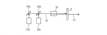
- FIG. 5 is a schematic diagram showing an embodiment of an optical device according to the present invention.
- the optical device includes first and second semiconductor lasers 22a and 22b having the same excitation frequency (for example, wavelength: 1.55 ⁇ m) arranged with a predetermined separation distance, First and second reflecting mirrors 23a and 23b for guiding laser light emitted from the second semiconductor lasers 22a and 22b onto the optical axis C1, LiNbO 3 disposed on the optical axis C1 and on which laser light is incident, etc.
- the infrared filter 6 of the present invention that filters the wavelength (1.55 ⁇ m) of the excitation light from the first and second semiconductor lasers 22a and 23b.
- the first semiconductor laser 22a and the second semiconductor laser 22b are used.
- a difference occurs in the oscillation frequency.
- the oscillation frequency of the first semiconductor laser 22a is ⁇ 1 and the oscillation frequency of the second semiconductor laser 22b is ⁇ 2
- the laser light (basic laser light) caused by the excitation frequency and the difference frequency light caused by the difference frequency ⁇ from the nonlinear optical crystal 24 have the same optical axis C1, Output onto C2.
- the said infrared filter 6 can filter the infrared ray (excitation light) of the near infrared region whose wavelength is 1.55 micrometer, only the difference frequency (DELTA) omega of a far-infrared ray with a large wavelength is optical axis C2. The light can be emitted upward, and only the difference frequency light can be easily extracted.
- the present invention is not limited to the above embodiment.
- the infrared filter 6 is exemplified as a flat plate, but may have a lens shape. In this case, various optical components having both a filter function and a lens function can be realized.
- Example preparation [Example 1] Polycrystalline silicon was produced using the CVD apparatus (FIG. 2) described in the section of [Best Mode for Carrying Out the Invention].
- a rod made of high-purity polycrystalline silicon having a diameter of 5 to 6 mm with a heater embedded therein was mounted in the reaction vessel to reduce the pressure, while the heater set temperature was raised to 850 ° C. Then, a raw material gas composed of high-purity SiHCl 3 and H 2 is introduced into the reaction vessel, SiHCl 3 is reduced, Si is deposited on the rod and deposited, whereby the sample of Example 1 (polycrystalline silicon) ) was produced.
- the purity of the produced polycrystalline silicon was measured and found to be 11N (99.99999999999%).
- Comparative Example 1 A sample (polycrystalline silicon) of Comparative Example 1 was produced in the same manner as in [Example 1] except that the heater set temperature was 1050 ° C. The purity of Comparative Example 1 was 11N.
- Comparative Example 2 Using the polycrystalline silicon of Comparative Example 1, single crystal silicon was produced by the FZ method.
- the polycrystalline silicon of Comparative Example 1 was placed in a container, and the polycrystalline silicon was melted by applying high frequency heating at an applied frequency of 3 MHz, and then using the seed crystal (single crystal silicon). The sample was re-solidified in the azimuth direction, thereby producing a sample of Comparative Example 2 (single crystal silicon). The purity was 11N.
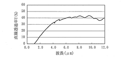
- Example evaluation The samples of Example 1 and Comparative Examples 1 and 2 were cut out in parallel and both surfaces were optically polished, and the infrared transmission spectrum was measured with a fast Fourier infrared spectrometer (FT-IR). That is, first, measure the blank value of each wavelength in the absence of the sample, then attach the sample to the measuring device and perform the same measurement, measure the linear transmittance from the ratio at each wavelength, and calculate the transmission spectrum. Obtained.
- FT-IR fast Fourier infrared spectrometer
- FIG. 6 shows the transmission spectrum of Example 1
- FIG. 7 shows the transmission spectrum of Comparative Example 1
- FIG. 8 shows the transmission spectrum of Comparative Example 2.
- the horizontal axis represents wavelength ( ⁇ m), and the vertical axis represents linear transmittance (%).
- Table 1 shows the ratio of the linear transmittance at a wavelength of 4 ⁇ m, a wavelength of 3 ⁇ m, and a wavelength of 2 ⁇ m, where the linear transmittance of infrared rays at a wavelength of 10 ⁇ m is 1.
- Example 1 and Comparative Example 1 the average crystal grain size of the crystal grains was measured. That is, each sample was mirror-polished and measured with an electron microscope / backscattered electron diffraction pattern (FE-SEM / EBSP) system, and using EBSP analysis software (TSL Solutions, OIM Analysis Ver. 4.6). The average particle size of the crystal particles was calculated.
- Table 2 shows the average crystal grain sizes of the samples of Example 1 and Comparative Example 1.
- the sample of Comparative Example 1 shows a linear transmittance substantially equal to the wavelength range of 8 to 12 ⁇ m even in the mid / near infrared range of 2 to 6 ⁇ m.
- the linear transmittances at the wavelength of 4 ⁇ m, the wavelength of 3 ⁇ m, and the wavelength of 2 ⁇ m were 1.03, 0.98, and 0.88, respectively, with respect to the linear transmittance of the wavelength of 10 ⁇ m. It was. Therefore, the infrared ray in the mid-infrared region becomes stray light and the S / N ratio is deteriorated, resulting in a decrease in the accuracy of human body detection. Therefore, it is not suitable as a transmission optical material for human body detection.
- Comparative Example 1 produced polycrystalline silicon at a high temperature of 1050 ° C., and as shown in Table 2, the average crystal grain size was coarsened to 10 ⁇ m.
- the sample of Comparative Example 2 also has a flat transmission spectrum in a wide wavelength range, and in the same way as Comparative Example 1, the wavelength is 8 to 8 in the mid / near infrared region of 2 to 6 ⁇ m.
- the linear transmittance is almost the same as the wavelength region of 12 ⁇ m.
- the linear transmittances at the wavelength of 4 ⁇ m, the wavelength of 3 ⁇ m, and the wavelength of 2 ⁇ m are the ratios of 1.05, 1.03, and 1.01, respectively, with respect to the linear transmittance of the wavelength of 10 ⁇ m. there were. Accordingly, as in Comparative Example 1, since the mid-infrared ray becomes stray light and the S / N ratio is deteriorated and the accuracy of human body detection is reduced, it is not suitable as a transmission optical material for human body detection.
- Comparative Example 2 is produced by the FZ method, so there are relatively few oxygen defects, and therefore it has good infrared transmission even in the wavelength region of 8-12 ⁇ m near 10 ⁇ m. It is thought that the transmittance in the mid-infrared region was increased because there was no scattering at the grain boundary.
- Example 1 since the heater set temperature is 850 ° C. and high-purity polycrystalline silicon is obtained, as shown in Table 2, the average crystal grain size can be reduced to 1 ⁇ m to 5 ⁇ m or less. The particles were able to avoid coarsening.
- the linear transmittance in the wavelength region of 4 ⁇ m or less is lower than the linear transmittance in the wavelength region of 8 to 12 ⁇ m.
- Table 1 compared to infrared light having a wavelength of 10 ⁇ m, infrared light having a wavelength of 4 ⁇ m transmits only 81%, infrared light having a wavelength of 3 ⁇ m transmits only 69%, and infrared light having a wavelength of 2 ⁇ m is 45%. % Was found to be transmitted.
- the sample of Example 1 has good linear transmittance in the wavelength region of 8 to 12 ⁇ m near 10 ⁇ m and can effectively absorb and scatter infrared rays having a wavelength of 4 ⁇ m or less.
Landscapes
- Physics & Mathematics (AREA)
- General Physics & Mathematics (AREA)
- Spectroscopy & Molecular Physics (AREA)
- Chemical & Material Sciences (AREA)
- Organic Chemistry (AREA)
- Inorganic Chemistry (AREA)
- Health & Medical Sciences (AREA)
- Toxicology (AREA)
- Optics & Photonics (AREA)
- Photometry And Measurement Of Optical Pulse Characteristics (AREA)
- Investigating Or Analysing Materials By Optical Means (AREA)
- Silicon Compounds (AREA)
Abstract
Description
すなわち、多結晶シリコン5は、化学反応式(1)に従って生成されてロッド2上に堆積し、これにより10N(テンナイン)から11N(イレブンナイン)の高純度の多結晶シリコンからなる透過光学材料を低コストで容易に得ることができる。
次いで、化学反応式(3)で示すように、金属級SiをHClと反応させる。金属級Siに含まれる各種金属不純物はBCl3やFeCl3等の塩化物の形態で除去され、これにより高純度のSiHCl3を得ることができる。
尚、SiHCl3の沸点は31.8℃であることから、蒸留精製を繰り返すことによって純度を向上させることができ、これにより11Nの高純度を有するSiHCl3を容易に得ることができる。
〔実施例1〕
〔発明を実施するための最良の形態〕の項で説明したCVD装置(図2)を使用して多結晶シリコンを作製した。
ヒータ設定温度を1050℃とした以外は、〔実施例1〕と同様の方法で比較例1の試料(多結晶シリコン)を作製した。尚、比較例1の純度は、11Nであった。
比較例1の多結晶シリコンを使用し、FZ法により単結晶シリコンを作製した。
実施例1、比較例1、2の各試料を平行に切り出して両面を光学研磨し、高速フーリエ赤外分光装置(FT-IR)によって赤外線の透過スペクトルを測定した。 すなわち、まず、試料の存在しない状態で各波長のブランク値を測定し、その後、測定装置に試料を装着して同様の測定を行い、各波長における比から直線透過率を測定し、透過スペクトルを得た。


3 反応容器
5 多結晶シリコン
6 赤外線フィルタ
22a 第1の半導体レーザ
22b 第2の半導体レーザ
24 非線形光学結晶
Claims (8)
- 高純度のトリクロロシランを原料として形成された多結晶シリコンからなり、4μm以下の波長域の赤外光線を吸収・散乱することを特徴とする赤外光線用透過光学部材。
- 波長4μmにおける赤外線の透過率Aと波長10μmにおける赤外線の透過率Bとの比A/Bが0.9以下であることを特徴とする請求項1記載の赤外光線用透過光学部材。
- 前記多結晶シリコンの平均結晶粒径が、5μm以下であることを特徴とする請求項1又は請求項2記載の赤外光線用透過光学部材。
- 前記多結晶シリコンは、化学蒸着法を使用して形成されていることを特徴とする請求項1乃至請求項3のいずれかに記載の赤外光線用透過光学部材。
- 反応容器に内蔵された基材を800~900℃の温度に加熱すると共に、高純度のトリクロロシラン及び水素を少なくとも含む原料ガスを前記反応容器に供給して前記トリクロロシランを還元し、前記基材上に多結晶シリコンを堆積することを特徴とする赤外光線用透過光学部材の製造方法。
- 主要部が、請求項1乃至請求項4のいずれかに記載の赤外光線用透過光学部材を備えたことを特徴とする光学デバイス。
- 赤外線検出器であることを特徴とする請求項6記載の光学デバイス。
- 同一の光軸上にレーザ光を出射する第1及び第2の半導体レーザと、前記光軸上に配されて前記レーザ光が入射される非線形光学結晶と、前記非線形光学結晶から出射されるレーザ光のうち特定波長域の光線をフィルタリングするフィルタ手段とを有し、
前記フィルタ手段が、請求項6記載の光学デバイスで構成されていることを特徴とする光学装置。
Priority Applications (3)
| Application Number | Priority Date | Filing Date | Title |
|---|---|---|---|
| JP2010544079A JP5246892B2 (ja) | 2008-12-24 | 2009-12-22 | 赤外光線用透過光学部材とその製造方法、光学デバイス、及び光学装置 |
| DE112009004379T DE112009004379T5 (de) | 2008-12-24 | 2009-12-22 | Infrarotstrahldurchlässiges optisches Element und Herstellungsverfahren dafür, optischeVorrichtung und optisches Gerät |
| US13/159,799 US8399836B2 (en) | 2008-12-24 | 2011-06-14 | Infrared ray transmissive optical member and manufacturing method thereof, optical device, and optical apparatus |
Applications Claiming Priority (2)
| Application Number | Priority Date | Filing Date | Title |
|---|---|---|---|
| JP2008-328241 | 2008-12-24 | ||
| JP2008328241 | 2008-12-24 |
Related Child Applications (1)
| Application Number | Title | Priority Date | Filing Date |
|---|---|---|---|
| US13/159,799 Continuation US8399836B2 (en) | 2008-12-24 | 2011-06-14 | Infrared ray transmissive optical member and manufacturing method thereof, optical device, and optical apparatus |
Publications (1)
| Publication Number | Publication Date |
|---|---|
| WO2010074074A1 true WO2010074074A1 (ja) | 2010-07-01 |
Family
ID=42287683
Family Applications (1)
| Application Number | Title | Priority Date | Filing Date |
|---|---|---|---|
| PCT/JP2009/071315 Ceased WO2010074074A1 (ja) | 2008-12-24 | 2009-12-22 | 赤外光線用透過光学部材とその製造方法、光学デバイス、及び光学装置 |
Country Status (4)
| Country | Link |
|---|---|
| US (1) | US8399836B2 (ja) |
| JP (1) | JP5246892B2 (ja) |
| DE (1) | DE112009004379T5 (ja) |
| WO (1) | WO2010074074A1 (ja) |
Cited By (4)
| Publication number | Priority date | Publication date | Assignee | Title |
|---|---|---|---|---|
| JP2011123185A (ja) * | 2009-12-09 | 2011-06-23 | Mitsubishi Materials Corp | 赤外線透過部材用シリコン材料及び赤外線透過部材 |
| US20120138803A1 (en) * | 2010-12-06 | 2012-06-07 | Takao Yamazaki | Infrared sensor package and electronic device equipped therewith |
| WO2016163419A1 (ja) * | 2015-04-08 | 2016-10-13 | 国立大学法人京都大学 | 赤外線透過部材用Cz-Siの加工方法、赤外線透過部材の製造方法および赤外線透過部材 |
| JP2018013375A (ja) * | 2016-07-20 | 2018-01-25 | 株式会社トーキン | 焦電型赤外線センサ装置 |
Families Citing this family (5)
| Publication number | Priority date | Publication date | Assignee | Title |
|---|---|---|---|---|
| JP5226883B2 (ja) * | 2011-02-01 | 2013-07-03 | Necトーキン株式会社 | 焦電型赤外線センサ |
| DE102013107189A1 (de) * | 2013-03-22 | 2014-09-25 | Schott Ag | Rohling aus Silizium, Verfahren zu dessen Herstellung sowie Verwendung desselben |
| WO2014147262A1 (de) | 2013-03-22 | 2014-09-25 | Schott Ag | Rohling aus silizium, verfahren zu dessen herstellung sowie verwendung desselben |
| JP6507779B2 (ja) * | 2015-03-26 | 2019-05-08 | セイコーエプソン株式会社 | 電気光学装置、電気光学装置の製造方法、および電子機器 |
| DE102015223362A1 (de) | 2015-11-25 | 2017-06-01 | Minimax Gmbh & Co. Kg | Explosionsgeschütztes Gehäuse für Mittel zum Senden und Empfangen elektromagnetischer Strahlung |
Citations (6)
| Publication number | Priority date | Publication date | Assignee | Title |
|---|---|---|---|---|
| JPH04315927A (ja) * | 1991-04-15 | 1992-11-06 | Horiba Ltd | 赤外線検出器 |
| JPH0560901A (ja) * | 1991-09-02 | 1993-03-12 | Matsushita Electric Ind Co Ltd | 赤外線光学素子およびその製造方法 |
| JPH06213725A (ja) * | 1992-05-27 | 1994-08-05 | Terumo Corp | 赤外線センサ用窓材 |
| JP2002234774A (ja) * | 2000-12-04 | 2002-08-23 | Sumitomo Electric Ind Ltd | セラミックス光学部品及びその製造方法 |
| JP2003042950A (ja) * | 2001-07-25 | 2003-02-13 | Oyo Kogaku Kenkyusho | ガス成分測定装置 |
| JP2004233802A (ja) * | 2003-01-31 | 2004-08-19 | Kobe Steel Ltd | 遠赤外光学部品 |
Family Cites Families (6)
| Publication number | Priority date | Publication date | Assignee | Title |
|---|---|---|---|---|
| DE2060839A1 (de) * | 1970-12-10 | 1972-06-29 | Siemens Ag | Infrarotlampe mit Kolben aus Silicium |
| US4148931A (en) * | 1976-03-08 | 1979-04-10 | Siemens Aktiengesellschaft | Process for depositing elemental silicon semiconductor material from a gas phase |
| KR880000618B1 (ko) * | 1985-12-28 | 1988-04-18 | 재단법인 한국화학연구소 | 초단파 가열 유동상 반응에 의한 고순도 다결정 실리콘의 제조 방법 |
| JP4315927B2 (ja) | 2005-03-24 | 2009-08-19 | 株式会社ソニー・コンピュータエンタテインメント | 記号分析装置、記号分析方法、プログラム及び情報記憶媒体 |
| JP5149512B2 (ja) * | 2007-02-02 | 2013-02-20 | 東レ・ダウコーニング株式会社 | 液状硬化性組成物、コーテイング方法、無機質基板および半導体装置 |
| ES2331824B1 (es) * | 2007-06-18 | 2010-10-22 | Consejo Superior De Investigaciones Cientificas (Csic) | Microcabidades opticas y esponjas fotonicas, procedimiento de producc ion y sus aplicaciones en la fabricacion de dispositivos fotonicos. |
-
2009
- 2009-12-22 DE DE112009004379T patent/DE112009004379T5/de not_active Ceased
- 2009-12-22 JP JP2010544079A patent/JP5246892B2/ja active Active
- 2009-12-22 WO PCT/JP2009/071315 patent/WO2010074074A1/ja not_active Ceased
-
2011
- 2011-06-14 US US13/159,799 patent/US8399836B2/en active Active
Patent Citations (6)
| Publication number | Priority date | Publication date | Assignee | Title |
|---|---|---|---|---|
| JPH04315927A (ja) * | 1991-04-15 | 1992-11-06 | Horiba Ltd | 赤外線検出器 |
| JPH0560901A (ja) * | 1991-09-02 | 1993-03-12 | Matsushita Electric Ind Co Ltd | 赤外線光学素子およびその製造方法 |
| JPH06213725A (ja) * | 1992-05-27 | 1994-08-05 | Terumo Corp | 赤外線センサ用窓材 |
| JP2002234774A (ja) * | 2000-12-04 | 2002-08-23 | Sumitomo Electric Ind Ltd | セラミックス光学部品及びその製造方法 |
| JP2003042950A (ja) * | 2001-07-25 | 2003-02-13 | Oyo Kogaku Kenkyusho | ガス成分測定装置 |
| JP2004233802A (ja) * | 2003-01-31 | 2004-08-19 | Kobe Steel Ltd | 遠赤外光学部品 |
Cited By (6)
| Publication number | Priority date | Publication date | Assignee | Title |
|---|---|---|---|---|
| JP2011123185A (ja) * | 2009-12-09 | 2011-06-23 | Mitsubishi Materials Corp | 赤外線透過部材用シリコン材料及び赤外線透過部材 |
| US20120138803A1 (en) * | 2010-12-06 | 2012-06-07 | Takao Yamazaki | Infrared sensor package and electronic device equipped therewith |
| US8785853B2 (en) * | 2010-12-06 | 2014-07-22 | Nec Corporation | Infrared sensor package and electronic device equipped therewith |
| WO2016163419A1 (ja) * | 2015-04-08 | 2016-10-13 | 国立大学法人京都大学 | 赤外線透過部材用Cz-Siの加工方法、赤外線透過部材の製造方法および赤外線透過部材 |
| JP2018013375A (ja) * | 2016-07-20 | 2018-01-25 | 株式会社トーキン | 焦電型赤外線センサ装置 |
| US11101422B2 (en) | 2016-07-20 | 2021-08-24 | Tokin Corporation | Pyroelectric infrared sensor device |
Also Published As
| Publication number | Publication date |
|---|---|
| US8399836B2 (en) | 2013-03-19 |
| JP5246892B2 (ja) | 2013-07-24 |
| JPWO2010074074A1 (ja) | 2012-06-21 |
| US20110243162A1 (en) | 2011-10-06 |
| DE112009004379T5 (de) | 2012-05-24 |
Similar Documents
| Publication | Publication Date | Title |
|---|---|---|
| JP5246892B2 (ja) | 赤外光線用透過光学部材とその製造方法、光学デバイス、及び光学装置 | |
| JP4233467B2 (ja) | 紫外線センサ及びその製造方法 | |
| US20130020484A1 (en) | Pyroelectric Element | |
| Li et al. | Direct Growth of Hexagonal Boron Nitride Thick Films on Dielectric Substrates by Ion Beam Assisted Deposition for Deep‐UV Photodetectors | |
| CN106525763B (zh) | 基于掺杂的石墨烯THz-SPR气体传感器系统及测试方法 | |
| CN103477207A (zh) | 多晶硅中碳浓度的测定方法 | |
| WO2013006151A2 (en) | Transitioned film growth for conductive semiconductor materials | |
| EP2471752B1 (en) | Method of manufacturing vitreous silica crucible | |
| Zhang et al. | Effect of surface carbon contamination on the chemical states of N-doped ZnO thin films | |
| JP2015105917A (ja) | 多結晶シリコン棒の表面温度測定方法および多結晶シリコンの製造方法 | |
| Khatami et al. | Annealing of silicon carbonitride nanostructured thin films: interdependency of hydrogen content, optical, and structural properties | |
| CN103842783B (zh) | 分光传感器 | |
| US9085480B2 (en) | Method of manufacturing vitreous silica crucible | |
| JP5895818B2 (ja) | SiC単結晶の評価方法およびそれを適用したSiC単結晶の製造方法 | |
| US9181121B2 (en) | Method for manufacturing vitreous silica crucible | |
| KR101606225B1 (ko) | 포토마스크용 광학 부재 및 그 제조 방법 | |
| CN104697960A (zh) | 光学元件及其制造方法 | |
| US12546658B2 (en) | Method for manufacturing a detection device comprising an encapsulation structure comprising a thin opaque layer resting on a mineral peripheral wall | |
| JP2010170081A (ja) | 遠赤外線用光学素子 | |
| JP7359322B2 (ja) | 四塩化ケイ素の測定ユニット、四塩化ケイ素の品質評価方法、四塩化ケイ素の品質管理方法、炭化ケイ素基板の製造方法、および、炭化ケイ素基板製造装置 | |
| US8689584B2 (en) | Method of manufacturing vitreous silica crucible | |
| JP2006211626A (ja) | 極低温冷却用窓材、天体観測装置用の極低温冷却装置、並びに、テラヘルツ波観測を利用した検査機器 | |
| Cui et al. | Infrared transmission and reflectivity measurements of 4H-and 6H-SiC single crystals | |
| WO2017115797A1 (ja) | シリコン材料、それを有する光学部材及び光学機器 | |
| JPS61257478A (ja) | 薄膜の形成法 |
Legal Events
| Date | Code | Title | Description |
|---|---|---|---|
| 121 | Ep: the epo has been informed by wipo that ep was designated in this application |
Ref document number: 09834875 Country of ref document: EP Kind code of ref document: A1 |
|
| ENP | Entry into the national phase |
Ref document number: 2010544079 Country of ref document: JP Kind code of ref document: A |
|
| WWE | Wipo information: entry into national phase |
Ref document number: 112009004379 Country of ref document: DE Ref document number: 1120090043798 Country of ref document: DE |
|
| 122 | Ep: pct application non-entry in european phase |
Ref document number: 09834875 Country of ref document: EP Kind code of ref document: A1 |