WO2010074012A1 - 画像補正処理回路、半導体装置、画像補正処理装置 - Google Patents
画像補正処理回路、半導体装置、画像補正処理装置 Download PDFInfo
- Publication number
- WO2010074012A1 WO2010074012A1 PCT/JP2009/071201 JP2009071201W WO2010074012A1 WO 2010074012 A1 WO2010074012 A1 WO 2010074012A1 JP 2009071201 W JP2009071201 W JP 2009071201W WO 2010074012 A1 WO2010074012 A1 WO 2010074012A1
- Authority
- WO
- WIPO (PCT)
- Prior art keywords
- image correction
- image
- register
- value
- correction processing
- Prior art date
- Legal status (The legal status is an assumption and is not a legal conclusion. Google has not performed a legal analysis and makes no representation as to the accuracy of the status listed.)
- Ceased
Links
Images




















































Classifications
-
- H—ELECTRICITY
- H04—ELECTRIC COMMUNICATION TECHNIQUE
- H04N—PICTORIAL COMMUNICATION, e.g. TELEVISION
- H04N5/00—Details of television systems
- H04N5/14—Picture signal circuitry for video frequency region
- H04N5/20—Circuitry for controlling amplitude response
-
- G—PHYSICS
- G06—COMPUTING OR CALCULATING; COUNTING
- G06T—IMAGE DATA PROCESSING OR GENERATION, IN GENERAL
- G06T5/00—Image enhancement or restoration
- G06T5/40—Image enhancement or restoration using histogram techniques
-
- G—PHYSICS
- G06—COMPUTING OR CALCULATING; COUNTING
- G06T—IMAGE DATA PROCESSING OR GENERATION, IN GENERAL
- G06T5/00—Image enhancement or restoration
- G06T5/90—Dynamic range modification of images or parts thereof
- G06T5/92—Dynamic range modification of images or parts thereof based on global image properties
-
- H—ELECTRICITY
- H04—ELECTRIC COMMUNICATION TECHNIQUE
- H04N—PICTORIAL COMMUNICATION, e.g. TELEVISION
- H04N1/00—Scanning, transmission or reproduction of documents or the like, e.g. facsimile transmission; Details thereof
- H04N1/40—Picture signal circuits
- H04N1/407—Control or modification of tonal gradation or of extreme levels, e.g. background level
- H04N1/4072—Control or modification of tonal gradation or of extreme levels, e.g. background level dependent on the contents of the original
- H04N1/4074—Control or modification of tonal gradation or of extreme levels, e.g. background level dependent on the contents of the original using histograms
-
- H—ELECTRICITY
- H04—ELECTRIC COMMUNICATION TECHNIQUE
- H04N—PICTORIAL COMMUNICATION, e.g. TELEVISION
- H04N5/00—Details of television systems
- H04N5/14—Picture signal circuitry for video frequency region
- H04N5/21—Circuitry for suppressing or minimising disturbance, e.g. moiré or halo
-
- G—PHYSICS
- G06—COMPUTING OR CALCULATING; COUNTING
- G06T—IMAGE DATA PROCESSING OR GENERATION, IN GENERAL
- G06T2207/00—Indexing scheme for image analysis or image enhancement
- G06T2207/30—Subject of image; Context of image processing
- G06T2207/30232—Surveillance
Definitions
- the present invention relates to an image correction processing circuit that performs various image correction processes on an input image to generate a desired output image, and a semiconductor device (image correction processing apparatus) formed by integrating the image correction processing circuit.
- the conventional image correction processing circuit generally divides one field of an input image into a plurality of areas, and what kind of scene the input image is based on a luminance histogram acquired for each area ( For example, it is determined whether it is foggy or backlit, and an optimal image correction process is performed on the input image.
- Patent Document 1 As an example of the related art related to the above, Patent Document 1 can be cited.
- 93A and 93B are block diagrams showing a conventional example of an electronic device (indoor / outdoor surveillance camera, network camera (IP camera), Web camera, in-vehicle camera, interphone, etc.) that handles image data.
- an electronic device indoor / outdoor surveillance camera, network camera (IP camera), Web camera, in-vehicle camera, interphone, etc.
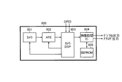
- the electronic apparatus 900 is a camera DSP [Digital] that performs various digital signal processing on input image data input from a camera 901 via an AFE [Analog Front End] 902 to generate output image data in a digital format.
- Signal Processor 903.
- Patent Document 2 can be cited.
- a fogged input image or a backlight input image can be converted into an output image with higher visibility and sent to a display device.
- the scene discrimination method employed in the conventional image correction processing circuit may not always obtain an appropriate scene discrimination result, and there is room for further improvement.
- a first technical means disclosed in the present specification is an image correction processing circuit capable of performing an appropriate image correction process on an input image and generating a desired output image.
- a first object is to provide a semiconductor device obtained by integrating the semiconductor device.
- the camera DSP 903 outputs the output image data generated by itself to a subsequent circuit (semiconductor memory or the like) in a digital format
- the image reproduction device that supports the output image data of the camera DSP 903 only for analog composite video input.
- the electronic device 900 is increased in size and cost.
- the second technical means disclosed in the present specification is an image correction capable of generating desired output image data by performing appropriate image correction processing on input image data.
- a second object is to provide a processing apparatus.
- an image correction processing circuit disclosed in the present specification includes: an image correction unit that performs a predetermined image correction process on an input image to generate an output image; A calculation unit that acquires a luminance histogram for each field of the image and calculates any two or three of the average luminance value, standard deviation value, and intermediate value; and the luminance histogram calculated by the calculation unit Based on any two or three of the average luminance value, standard deviation value, and intermediate value of the image, the necessity and amount of image correction processing for the input image are determined, and the image correction unit is controlled. And a correction control unit (1-1 configuration).
- the image correction unit performs fog image correction processing on the input image, and the correction control unit performs averaging of the luminance histogram. It is preferable to adopt a configuration (1-2 configuration) for determining the necessity and correction amount of the fog image correction processing based on the luminance value and the standard deviation value.
- the correction control unit has an average luminance value of the luminance histogram larger than a first threshold value, and a standard deviation value of the luminance histogram is a second threshold value. If it is smaller than the above, it may be configured to determine that the fog image correction process is necessary (configuration 1-3).
- the correction control unit determines that the fog image correction process is necessary, the smaller the standard deviation value of the luminance histogram, A configuration in which the correction amount of the fog image correction processing is set to be large stepwise or continuously (configuration 1-4) is preferable.
- a hysteresis width is set in at least one of the first threshold and the second threshold (first-first 5 configuration).
- the image correction processing circuit having any one of the above-described configurations 1-1 to 1-5 is variously referred to by the correction control unit when determining the necessity of the image correction processing for the input image and the correction amount. It is preferable to adopt a configuration (1-6 configuration) having a register for externally setting the parameters.
- the semiconductor device disclosed in the present specification has a configuration (first 1-7 configuration) in which image correction processing circuits having any one of the first to first to sixth configurations are integrated. Has been.
- an image correction processing device in the present specification includes a first external terminal to which input digital image data is input from the outside of the device; An image correction processing circuit that performs predetermined image correction processing on the image data to generate digital output image data; a second external terminal that outputs the digital output image data outside the apparatus; An encoder circuit that converts output image data into output image data in analog composite video format; and a third external terminal that outputs the output image data in analog composite video format outside the apparatus (second configuration) -1 configuration).
- the image correction processing circuit is an image correction process based on a luminance histogram for the input image data in the digital format.
- a first image correction that generates intermediate image data in a digital format by applying a first image correction process that may cause a loss of balance of color components or a secondary insufficiency of luminance dynamic range.
- a second image correction process that eliminates the color component imbalance caused by the first image correction process or the lack of luminance dynamic range on the digital intermediate image data;
- a second image correction processing unit for generating the output image data in the digital format (configuration 2-2).
- the first image correction process is a fog image correction process
- the second image correction process is a color correction process or a luminance dynamic process.
- a configuration that is range correction (configuration 2-3) is preferable.
- the first image correction processing unit can vary an effective luminance range of the luminance histogram referred to when calculating a correction coefficient. (2-4 configuration).
- the first image correction processing unit inputs the correction coefficient of the frame and the frame before and after the frame when determining the correction coefficient of the frame. It is preferable to use a correction coefficient of at least one frame that is subjected to low-pass filter processing (second to fifth structure).
- FIG. 1 is a block diagram showing a first embodiment of an image processing IC according to the present invention.
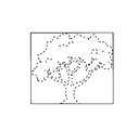
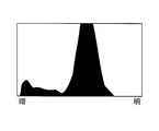
- Schematic diagram showing a foggy image Schematic diagram showing the brightness histogram of foggy images
- Flowchart for explaining necessity determination of fog image correction processing The figure for demonstrating the comparison determination operation
- latter stage of a 1st image correction process part Diagram for explaining variation of luminance histogram
- the figure for demonstrating the cause of flicker generation accompanying an image correction process The block diagram which shows the 1st structural example of a 1st image correction process part. Illustration for specifying effective range of luminance histogram
- Schematic diagram for explaining the low-pass filter processing (when calculating the calculation parameter of field 3) 1 is a diagram showing an example of the configuration of an electronic device equipped with an image processing IC according to the present invention.
- the figure which shows another example of a structure of the electronic device carrying the image processing IC which concerns on this invention 1 is a block diagram showing a first conventional example of an electronic device that handles image data
- FIG. 1 is a block diagram showing a first embodiment of an image processing IC according to the present invention.
- the image processing IC 10 of this embodiment is a semiconductor device in which an image correction processing circuit including a fog image correction unit 11, a luminance histogram calculation unit 12, a correction control unit 13, and a register 14 is integrated. is there.
- the image processing IC 10 has various image processing (luminance dynamic range correction, brightness correction, backlight correction, etc.) for the input image in addition to the fog image correction unit 11. It is possible to include a circuit block that applies
- the fog image correction unit 11 is a unit that performs a fog image correction process on the input image input from the image source 20 to generate a desired output image and outputs it to the display device 30.
- the image source 20 is a means for generating an input image input to the image processing IC 10, and for example, a digital video camera that performs moving image shooting, a digital still camera that performs still image shooting, or the like can be used.
- the image source 20 includes a broadcast receiver (digital television broadcast receiver, etc.) and a media playback device (video CD, DVD, Blu-ray disc, hard disk, semiconductor memory, and other drive devices having a playback function, It is also possible to use a personal computer equipped with a video content playback function provided via the Internet.
- the display device 30 is means for displaying an output image that has been subjected to fog image correction processing by the image processing IC 10, and an LCD [Liquid Crystal Display], an organic EL [Electro-Luminescence] display, or the like can be used.
- the luminance histogram calculation unit 12 acquires a luminance histogram for each field (frame) of the input image input from the image source 20, and any one of the average luminance value, the standard deviation value, and the intermediate value is binary or three. It is a means for calculating all values.
- the luminance histogram calculation unit 12 is configured to calculate the average luminance value ACAVG and the standard deviation value ACVRC of the luminance histogram.
- the correction control unit 13 is a fog image correction process for the input image based on any two or three values of the average luminance value, the standard deviation value, and the intermediate value of the luminance histogram calculated by the luminance histogram calculation unit 12. Is a means for determining the necessity and the amount of correction, and controlling the fog image correction unit 11 based on the determination result. In the example of FIG.
- the correction control unit 13 compares the average luminance value ACAVG of the luminance histogram with the first threshold value (ACAVGTH1, ACAVGTH2), the standard deviation value ACVRC of the luminance histogram, and The second comparison unit 132 that compares the second threshold values (ACVRCTH1 to ACVRCTH3), and the determination that determines whether or not the fog image correction process is necessary and the correction amount based on the comparison results of the first comparison unit 131 and the second comparison unit 132 Part 133.
- the control operation of the fog image correction unit 11 by the correction control unit 13 will be described in detail later.
- the register 14 stores various parameters (including the first threshold value and the second threshold value described above) that are referred to by the correction control unit 13 when determining whether or not the fog image correction process is necessary for the input image and the correction amount.
- This is parameter storage means for external setting from the microcomputer 40.
- FIGS. 3A and 3B are schematic diagrams showing an input image without fog and its luminance histogram, respectively.
- an input image with fog (FIG. 2A) is generally white (brighter) and has a low contrast (narrow luminance dynamic range) compared to an input image without fog (FIG. 3A).
- the luminance histogram of the input image with fog is higher in average luminance value and smaller in standard deviation value than the luminance histogram of the input image without fog (FIG. 2B, FIG. 3B).
- the correction control unit 13 determines whether or not the fog image correction processing is necessary for the input image and the correction amount based on the average luminance value ACAVG and the standard deviation value ACVRC of the luminance histogram calculated by the luminance histogram calculation unit 12. It is set as the structure which determines and controls the fog image correction
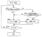
- FIG. 4 is a flowchart for explaining the necessity determination of fog image correction processing by the correction control unit 13 (particularly the determination unit 133).
- the register value FR_AT is set to “1 (fog image correction process: automatic)”
- the register value FR_EN is set to “0 (fog image correction process: stopped)”.
- the register value FR_AT is a register value for setting a method for executing fog image correction processing.
- the register value FR_AT is set to “0”
- the fog image correction process is executed manually.
- the register value FR_AT is set to “1”
- the fog image correction process is automatically executed.
- the register value FR_AT is set to “1”
- the bit control of the register value FR_EN is also automatically performed.
- the register value FR_EN is a register value for performing operation control (enable control) or operation confirmation of fog image correction processing.
- the register value FR_AT is set to “0 (mist image correction process: manual)”
- the register value FR_EN is used for operation control (enable control) of the fog image correction process. That is, when the register value FR_EN is set to “0”, the fog image correction process is disabled, and when the register value FR_EN is set to “1”, the fog image correction process is enabled.
- the register value FR_AT is set to “1 (fog image correction process: automatic)”
- the register value FR_EN is used to check the operation of the fog image correction process. That is, when the register value FR_EN is set to “0”, it is confirmed that the fog image correction process is stopped.
- the register value FR_EN is set to “1”, the fog image correction process is in operation. It is confirmed that there is.
- step S1 a comparison determination is made between the average luminance value ACAVG of the luminance histogram and the first threshold value (upper threshold ACAVGTH1 in step S1). If it is determined that ACAVG ⁇ ACAVGTH1, the flow proceeds to step S2 (correction amount adjustment state). On the other hand, if it is determined that ACAVG ⁇ ACAVGTH1, the flow proceeds to step S4.
- the correction amount adjustment process in step S2 will be described in detail later.
- step S4 determines whether or not the register value FR_EN is set to “1”, and the average luminance value ACAVG of the luminance histogram and the first Is compared with the threshold value (the lower threshold value ACAVGTH2 ( ⁇ ACAVGTH1) in step S4).
- the register value FR_EN is set to “1” and it is determined that ACAVG ⁇ ACAVGTH2, the flow proceeds to step S2 described above.
- the register value FR_EN is not set to “1” or that ACAVG ⁇ ACAVGTH2, the flow proceeds to step S5.
- step S3 the register value FR_AT is set to “0 (mist image correction process: manual)”. A determination is made whether or not it has been done. If it is determined that the register value FR_AT is not set to “0”, the flow is returned to step S1, and the average luminance value ACAVG of the luminance histogram and the first threshold value (the upper threshold value in step S1). Comparison determination with ACAVGTH1) is repeated. On the other hand, when it is determined that the register value FR_AT is set to “0”, a series of flows is terminated in order to switch the fog image correction process to manual execution.
- the first threshold value to be compared with the average luminance value ACAVG of the luminance histogram it is desirable to set a predetermined hysteresis width by adjusting the upper threshold value ACAVGTH1 and the lower threshold value ACAVGTH2 as described above. .
- Both the upper threshold ACAVGTH1 and the lower threshold ACAVGTH2 can be externally set in the register 14 from the microcomputer 40. When the upper threshold ACAVGTH1 and the lower threshold ACAVGTH2 are set to the same value, the above hysteresis is set. The function is turned off.
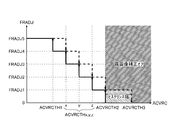
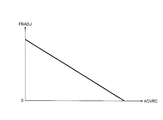
- FIG. 6A is a diagram illustrating an example of the correction amount adjustment process.
- the horizontal axis of FIG. 6A shows the standard deviation value ACVRC of the luminance histogram, and the vertical axis of FIG. 6A shows the register value FRADJ for setting the correction amount (correction intensity) of the fog image correction process. It is shown.
- the correction control unit 13 performs a comparison determination between the standard deviation value ACVRC of the luminance histogram and the second threshold values (ACVRCTH1 to ACVRCTH3, ACVRCTHx to ACVRCTHz), and the fog image for the input image Whether correction processing needs to be performed and, if fog image correction processing needs to be performed on the input image, whether the correction amount (correction strength) should be set to one of the register values FRADJ1 to FRADJ5 Judgment is made.
- three threshold values (ACVRCTH1, ACVRCTH2, ACVRCTH3) can be externally set in the register 14 from the microcomputer 40, and the remaining three threshold values (ACVRCTHx, ACVRCTTHy, ACVRCTHz) are
- the threshold value ACVRCTH1 and the threshold value ACVRCTH2 are automatically set in the form of being divided into four equal parts. Therefore, when the three threshold values (ACVRCTH1, ACVRCTH2, and ACVRCTH3) among the second threshold values are externally set, it is necessary to satisfy the relationship of ACVRCTH1 + 4 ⁇ ACVRCTH2 ⁇ ACVRCTH3.
- the register values FRADJ1 to FRADJ5 that are candidate values for the correction amount can be externally set in the register 14 from the microcomputer 40.
- the second threshold values ACVRCTH1 to ACVRCTH3, ACVRCTHx to ACVRCTHz
- the first threshold values ACAVGTH1 and ACAVGTH2
- FIG. 6A when the standard deviation value ACVRC of the luminance histogram gradually decreases (when the correction amount needs to be increased), the correction amount is adjusted along the path indicated by the solid line, When the standard deviation value ACVRC of the histogram gradually increases (when it is necessary to reduce the correction amount), the correction amount may be adjusted along the path indicated by the broken line.
- ACVRC ACVRCTHy is determined at the time of the previous comparison determination, and the current correction amount is set to the register value FRADJ3.
- the correction amount is not switched to the register value FRADJ4 until the standard deviation value ACVRC of the luminance histogram falls below the threshold value ACVRCTHx (see the solid line in FIG. 6A).
- the standard deviation value ACVRC of the luminance histogram is the threshold value ACAVGTHz.
- the correction amount is not switched to the register value FRADJ2 until the above is reached (see the broken line in FIG. 6A). Therefore, it is possible to prevent the fog image correction processing from being frequently switched, and to suppress flickering of the output image.
- the fog image correction process When the fog image correction process is turned off, the fog image correction process is turned on when the standard deviation value ACVRC of the luminance histogram falls below the threshold value ACVRCTH2, and the correction according to the standard deviation value ACVRC of the luminance histogram is performed. The amount adjustment process is started (see the solid line in FIG. 6A).
- the fog image correction process is once turned on, even if the standard deviation value ACVRC of the luminance histogram is equal to or greater than the threshold value ACVRCTH2, the fog image correction process is maintained in the on state, and the standard deviation value ACVRC is equal to or greater than the threshold value ACVRCTH3. At that time, the fog image correction process is turned off (see the broken line in FIG. 6A).
- the on / off oscillation of the fog image correction process can be prevented and flickering of the output image can be suppressed.
- the threshold value ACVRCTH3 is set to the maximum value that can be taken by the standard deviation value ACVRC of the luminance histogram, the fog image correction process is always turned on.
- the correction control unit 13 determines that the average luminance value ACAVG of the luminance histogram is greater than the first threshold value (the threshold value ACAVGTH1 or the threshold value ACAVGTH2 in the examples of FIGS. 4 and 5).
- the second threshold value threshold value ACVRCTH2 or ACVRCTH3 in the example of FIG. 6A
- the area division process of the input image is not required.
- Appropriate scene discrimination can be performed and optimal fog image correction processing can be performed for each scene, so that the visibility of the output image can be improved.
- the frequency of updating is not necessarily limited to one field, and can be arbitrarily adjusted according to the register setting from the microcomputer 40, such as every 16 fields, every 32 fields, or every 64 fields.
- the image processing IC 10 according to the present invention is used. If hardware arithmetic processing is performed, the load on the microcomputer 40 can be reduced, so that the processing speed can be improved and the cost can be reduced as a whole system.
- the configuration in which the present invention is applied to the fog image correction processing circuit has been described as an example.
- the application target of the present invention is not limited to this, and other image correction is performed.
- the present invention can be widely applied to processing circuits. For example, if the present invention is applied to the backlight image correction processing circuit, a luminance histogram is acquired for each frame of the input image, the average luminance value is relatively low, the standard deviation value is relatively large, and If the intermediate value is relatively high, the input image may be recognized as being backlit and the backlight correction process may be performed.
- the correction amount of the fog image correction process is increased stepwise as the standard deviation value ACVRC of the luminance histogram is smaller.
- the configuration to be set has been described as an example, but the configuration of the present invention is not limited to this.
- a configuration in which the processing correction amount is continuously set to a large value may be used.
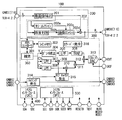
- FIG. 7 is a block diagram showing a second embodiment of the image processing IC according to the present invention.
- the image processing IC 100 includes a semiconductor device (with an image correction function) in which an image correction processing circuit 200, an encoder circuit 300, a first serial interface circuit 400, and a second serial interface circuit 500 are integrated.
- Digital video encoder IC which has both a function as an NTSC / PAL digital video encoder and a function as a fog correction / dynamic range correction image processing apparatus.
- the image processing IC 100 according to the present embodiment is integrated with registers for storing operation setting parameters of each part of the IC.
- the image correction processing circuit 200 is a circuit block that generates digital output image data by performing predetermined image correction processing on digital input image data input from the outside of the apparatus.
- a correction processing unit 201 and a second image correction processing unit 202 are provided.
- the first image correction processing unit 201 is a circuit block that performs fog image correction processing on digital-format input image data input from the outside of the apparatus.
- the luminance histogram calculation unit 12 and the correction control unit 13 correspond to this.
- the second image correction processing unit 202 further performs color correction processing and luminance dynamic range correction processing on the input image data that has been subjected to fog image correction processing and is input from the first image correction processing unit 201. And a color correction unit 202a, a luminance determination unit 202b, an image enhancement unit 202c, and an arithmetic processing unit 202d.
- the color correction unit 202a calculates a color correction coefficient based on the fogged image corrected processed input image data input from the first image correction processing unit 201.
- the luminance determination unit 202b calculates a luminance dynamic range correction coefficient based on the input image data that has been subjected to the fog image correction process and is input from the first image correction processing unit 201.
- the image enhancement unit 202c calculates a final image correction coefficient based on the color correction coefficient input from the color correction unit 202a and the luminance dynamic range correction coefficient input from the luminance determination unit 202b.
- the arithmetic processing unit 202d Based on the final image correction coefficient input from the image enhancement unit 202c, the arithmetic processing unit 202d further applies the fog image correction processed input image data input from the first image correction processing unit 201. Then, color correction processing and luminance dynamic range correction processing are performed.
- the encoder circuit 300 is a circuit block that converts output image data in digital format generated by the image correction processing circuit 200 into output image data in analog composite video format, and includes a memory controller 301, a line memory 302, and a complementing unit 303.
- a subcarrier signal generation unit 315 and a color bar signal generation unit 316 A subcarrier signal generation unit 315 and a color bar signal generation unit 316.
- the memory controller 301 uses the line memory 302 to perform line buffer control of output image data in digital format input from the image correction processing circuit 200.
- the complementing unit 303 performs deficient information complementing processing (YUV (4: 2: 2) ⁇ YUV (4: 4: 4)) on the digital output image data input from the memory controller 301, and Oversampling processing (13.5 MHz ⁇ 27 MHz) is performed.
- the gamma correction unit 304 performs gamma correction processing on the luminance signal Y input from the complementing unit 303.
- the low pass filter unit 305 performs low pass filter processing on the output signal of the gamma correction unit 304.
- the trap filter unit 306 performs band elimination filter processing on the output signal of the low pass filter unit 305.
- the low-pass filter units 307 and 308 perform low-pass filter processing on the color difference signals Cb and Cr input from the complementing unit 303, respectively.
- Arithmetic processing units 309 and 310 superimpose subcarrier signals on the output signals of low-pass filter units 307 and 308, respectively.
- the arithmetic processing unit 311 adds the output signal of the arithmetic processing unit 309 and the output signal of the arithmetic processing unit 310.
- the arithmetic processing unit 312 adds the output signal of the trap filter unit 305 and the output signal of the arithmetic processing unit 311.
- the digital / analog conversion unit 313 converts the digital signal input from the arithmetic processing unit 312 into an analog signal and outputs the analog signal.
- the timing signal generator 314 outputs a timing signal (horizontal synchronization signal, vertical synchronization signal, clock signal) input from the outside of the apparatus as it is to the outside of the apparatus as it is, while using the timing signal, the subcarrier signal generation section 315 Synchronous control is also performed.
- the subcarrier signal generation unit 315 generates a subcarrier signal used for burst modulation of the color difference signals Cb and Cr and supplies it to the arithmetic processing units 309 and 310.
- the color bar signal generation unit 316 generates a color bar signal that serves as a reference value for output image data in the analog composite video format.
- the first serial interface circuit 400 performs two-wire serial communication with peripheral devices (such as a CPU [Central Processing Unit]) according to the I 2 C [Inter-Integrated Circuit] standard.
- peripheral devices such as a CPU [Central Processing Unit]
- I 2 C Inter-Integrated Circuit
- the second serial interface circuit 500 performs serial communication according to the SPI [Serial Peripheral Interface] standard with the EEPROM [Electrically Erasable and Programmable Read Only Memory].
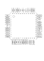
- FIG. 8 is a terminal layout diagram of the image processing IC 100
- FIG. 9 is a terminal function explanatory table of the image processing IC 100.
- Pin 1 is an SPI bus data input terminal.
- Pins 2 (CAMDI7) to 5 (CAMDI4) are data input terminals (upper 4 bits [7: 4]).
- Pin 6 is a common ground terminal.
- Pin 7 (VDD) is a core power supply terminal.
- Pins 8 (CAMDI3) to 11 (CAMDI0) are data input terminals (lower 4 bits [3: 0]), respectively.
- Pin 12 (CAMHSI) is a horizontal timing input terminal.
- Pin 13 (CAMVSI) is a vertical timing input terminal.
- Pin 14 (CAMCKI) is a clock input terminal.
- Pin 15 (GND) is a common ground terminal.
- Pin 16 (VDDIO) is a digital I / O power supply terminal.
- Pins 17 (CAMDO0) to 24 (CAMDO7) are data output terminals (all 8 bits [7: 0]).
- Pin 25 (CAMHSO) is a horizontal timing output terminal.
- Pin 26 (CAMVSO) is a vertical timing output terminal.
- Pin 27 (CAMCKO) is a clock output terminal.
- the 28th pin (GND) is a common ground terminal.
- Pin 29 (VDD) is a core power supply terminal.
- Pin 30 (AUTO) is an automatic register setting function valid terminal.
- Pin 31 (MODE0) and pin 32 (MODE1) are mode selection terminals.
- Pin 33 (VOUT) is an analog composite video output terminal.
- Pin 34 (AVSS) is an analog ground terminal for DAC.
- Pin 35 (IREF) is a DAC reference voltage output terminal.
- Pin 36 is a DAC analog power supply terminal.
- Pin 37 is a common ground terminal.
- the 38th pin (VDDI2C) is a 2-wire serial interface digital I / O power supply terminal.
- the 39th pin (SDA) is a 2-wire serial interface input / output data terminal.
- Pin 40 (SDC) is a 2-wire serial interface input / output clock terminal.
- Pin 41 (RESETB) is a system reset signal input terminal.
- Pin 42 (TEST) is a test mode terminal, and is connected to the ground in use.
- Pin 43 (GND) is a common ground terminal.
- the 44th pin (VDDIO) is a digital I / O power supply terminal.
- the 45th pin (WPB) is an EEPROM write protect terminal.
- the 46th pin (SCEB) is an EEPROM chip select terminal.
- Pin 47 (SCK) is an SPI bus clock output terminal.
- the 48th pin (SDO) is an SPI bus data output terminal.
- the active level of a terminal displayed with “*” in the active level column in FIG. 9 can be changed by setting the register. Further, the Init column in FIG. 9 shows the pin state at the time of reset release. In addition, terminals with “* 1” displayed in the Init column indicate that they are in a pull-down state. Further, regarding the numbers described in the power supply system column in FIG. 9, “1” represents VDDIO, “2” represents VDDI2C, “3” represents AVDD, and “4” represents VDD.
- the 2nd pin (CAMDI7) to 5th pin (CAMDI4) and the 8th pin (CAMDI3) to 11th pin (CAMDI0) are the first ones to which input image data in digital format is input from the outside of the IC.
- Pins 17 (CAMDO0) to 24 (CAMDO7) correspond to second external terminals that output digital output image data outside the IC.
- Pin 33 (VOUT) corresponds to a third external terminal for outputting output image data in analog composite video format outside the IC.
- the image processing IC 100 integrates fog image correction, color correction processing, and luminance dynamic range correction processing, so that an input video input from a camera or the like (particularly, an input image with fog or low illuminance)
- This is a video encoder with a built-in image correction function capable of improving the visibility of an input image or an input image in a backlight state.
- the first feature is that it supports ITU-R BT.656-4 or YCbCr with sync signal as the input data format.
- the data bus width is 8 bits and the pixel clock is 27 MHz.
- the data bus width is 8 bits and the data range is full range or compliant with ITU-R BT.601.
- Pixel clock is NTSC (27MHz, 28.63636MHz or 19.06993MHz), PAL (27MHz, 28.375MHz, 35.46895MHz or 18.9375MHz).
- the second feature is that the output data format is compatible with ITU-R BT.656-4 or YCbCr with a synchronization signal, like the input format.
- the third feature is that it supports NTSC / PAL SD-TV composite video output (CVBS) as an output video format.
- a fourth feature is that an image correction function (fog image correction function, color correction function, luminance dynamic range correction function), an edge enhancement filter, and a gamma filter are incorporated.
- a fifth feature is that one channel of a 10-bit digital / analog converter is incorporated.
- a sixth feature is that a slave function using a two-wire serial interface is incorporated, and a register in the IC can be set from the outside.
- the seventh feature is that the SPI bus master function is built-in, and the register set value stored in the external EEPROM can be automatically read and set in the IC internal register at reset release and mode change. It is.
- the ninth feature is that a 48-pin VQFP package (0.5 mm pin pitch) is adopted.
- the range of input digital data can be set by the ITU601R_I register.
- the LEVEL register can set an analog signal level when the digital data is output in CVBS.
- the relationship between the digital data range by the ITU601R_I register and the CVBS output level by the LEVEL register is as shown in FIGS. 10A and 10B.
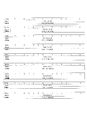
- 10A and 10B are diagrams illustrating the level relationship between the digital data and the CVBS output for each setting.
- FIG. 10A shows a state when 100 [IRE] is set
- FIG. 10B shows a state when 108 [IRE] is set.
- FIG. 11A is a data transmission / reception waveform diagram of the 2-wire serial interface
- FIG. 11B is a format diagram of the 2-wire serial interface.
- the slave address of the 2-wire serial interface is 70h.
- the sub address is automatically incremented when two or more consecutive accesses are performed for both writing and reading.
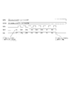
- FIG. 12 is a data transmission / reception waveform diagram of the SPI bus interface.
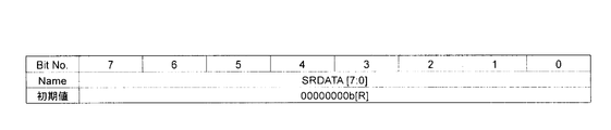
- REG_WPB, REG_SCEB, SWDATA, and SRDATA in FIG. 12 are register names, and each function is as follows.
- REG_WPB Specifies the logic of the WP pin. The register value is output as is to the WP pin.
- REG_SCEB Specifies the logic of the SCEB pin. The register value is output as is to the SCEB pin.
- CAMCKI is 27MHz
- SCK is 13.5MHz to 3.3kHz.
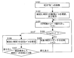
- FIG. 13 is a flowchart showing an automatic data reading sequence.
- step S101 the RESETB pin is released.
- step S102 the logical levels of MODE0 and MODE1 are confirmed and the confirmation results are stored.
- step S103 data is read from the EEPROM.
- step S104 it is determined whether the operation state is a set state or a stop state. If it is determined in step S104 that the set state, the data is reflected in the target index in step S105. On the other hand, if the stop state is determined in step S104, the logical levels of MODE0 and MODE1 are confirmed in step S106.
- step S107 the state of the MODE pin stored in step S102 is compared with the confirmation result in step S106. If it is determined that there is a change, the flow is returned to step S103. If it is determined that there is no change, the flow is returned to step S106.
- step S103 in FIG. 13 when data is read from the EEPROM, the read start address ST_ADR of the EEPROM follows the settings of the MODE0 pin and the MODE1 pin as follows.
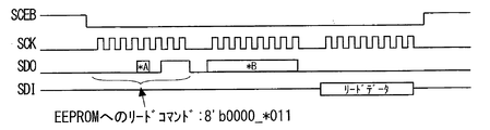
- FIG. 14 is a waveform diagram for explaining the flow of reading data from the EEPROM.
- “* A” is the EEPROM address bit8
- “* B” is the EEPROM address bit7-bit0.
- step S105 in FIG. 13 when data is reflected in the target index, the register value is reflected in the IC according to the data format in the EEPROM.
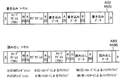
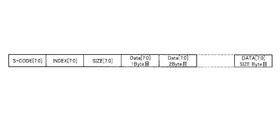
- 15A and 15B are diagrams showing a data format inside the EEPROM. Note that FIG. 15A shows a data format at the time of setting (operation state in which setting is made to a register in the IC), and FIG. 15B shows a data format at the time of stop (automatic reading stop state).
- the data contents in FIG. 15A are as follows. S-CODE: 8'b0000_0001.
- the image processing IC 100 receives this code and determines that the subsequent data is a valid register value.
- Index Setting start index address of this IC Size: Number of set sizes (bytes)
- Data Setting data. The number of data is Size bytes
- FIG. 15B the data content of FIG. 15B is as follows.
- the automatic reading function determines the index value as the setting start address of this IC, and performs setting continuously for Size.
- the setting / stop determination is performed again. If the setting is set, the setting for Size is performed using the index as the setting start address. This operation is performed until a stop is identified. Once the stop is identified, the automatic reading function is temporarily stopped. Thereafter, MODE0 and MODE1 are polled every time set by the polling interval, and when the pin level change is confirmed, the operation is started again. In addition, if MODE0 and MODE1 are changed while the automatic reading function is operating, resetting is performed immediately after the automatic reading operation is completed.
- FIG. 16 is a register map of the image processing IC 100. Note that access to registers in Empty notation and Reserved notation is prohibited.
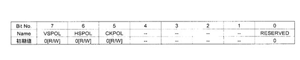
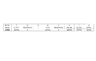
- FIG. 17 is a detailed table of the polarity setting register POL. IDX_ADDRESS is 10h.
- CKPOL sets the polarity of CAMCKI with respect to CAMDI [7: 0]. The settings are as follows. “0": Data change at the falling edge of CAMCKI, data capture at the rising edge (see Figure 18A) "1": Data change at the rising edge of CAMCKI, data capture at the falling edge (see Figure 18B)
- HSPOL sets the polarity of the horizontal sync signal (CAMHSI). HIGH section is valid data (LOW is sink section). HSPOL should be set to "0".
- VSPOL sets the polarity of the vertical sync signal (CAMVSI). HIGH section is valid data (LOW is sink section). Set VSPOL to "0".
- FIG. 19 is a detailed table of the parameter update register PARAMSET. IDX_ADDRESS is 11h.
- Parameter is updated by writing "1" to PARAM_SET.
- the internal parameters are updated at the beginning of the frame after writing. This bit is automatically cleared after update.
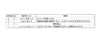
- FIG. 20 is a detailed table of the mode register MODE. IDX_ADDRESS is 12h.
- MODE [1: 0] sets the image enhancement operation mode of this IC (see FIG. 21).
- TH_TYPE sets the operation mode of the through mode. In the through mode, the data and the synchronization signal are output after delaying the same number of cycles as in the image enhancement mode. TH_TYPE should be set to “1”.
- SUSP sets IO suspend mode.
- the CAMDI0-7, CAMHSI, CAMVSI, and CAMCKI signals are not transmitted to the IC.
- the settings are as follows. "0": Suspend mode released "1": Suspend mode
- PD_OFF controls the pull-down setting of AUTO, MODE0, and MODE1 of this IC.
- the settings are as follows. “0”: Built-in pull-down resistor is connected to each of AUTO, MODE0, and MODE1. “1”: The built-in pull-down resistor is disconnected from each of AUTO, MODE0, and MODE1.
- DOUT_OFF controls the digital output setting of this IC.
- the settings are as follows. “0”: Image data is output from the digital terminal. “1”: CAMDO0-7, CAMHSO, CAMVSO, and CAMCKO are output low.
- FR_OUT_SEL selects whether to output CAMHSO whose timing is internally adjusted from CAMHSI or FR_EN (IDX_ADDRESS: 30h bit [0]) to the CAMHSO terminal.
- the settings are as follows. "0": Output CAMHSO “1”: Output FR_EN
- FIG. 22 is a detailed table of the input interface format designation register YUVIFSET. IDX_ADDRESS is 13h.
- YUV_XST [1: 0] sets the delay until the data becomes valid after Hsync is valid.
- YUV_XST [1: 0] may be set to “0”.
- YUVORD [1: 0] sets the YCbCr input format.
- YUVORD [1: 0] should be set to “10b” (CbYCrY).
- ITU601R selects the digital interface data range. Settings other than the following are prohibited. “00b”: Performs data input / output in the full range. “11b”: Data is input / output within the ITU601 range.
- ITU656EN sets input and output digital interfaces. The settings are as follows. "0": Hsync / Vsync separate signal "1": ITU656 format
- FIG. 23 is a detailed table of the output range conversion register TRAM_LIM. IDX_ADDRESS is 49h.
- TRAN_LIM performs color space conversion (YUV ⁇ RGB ⁇ YUV conversion) on the digital output signal: CAMDO7-0.
- color space conversion YUV ⁇ RGB ⁇ YUV conversion
- the output chroma components are limited to values that can be expressed in RGB space. The settings are as follows. "0": With color space conversion "1": Without color space conversion
- FIG. 24 is a detailed table of the monitor X direction pixel size setting register DXSIZE.
- IDX_ADDRESS is 14h and 15h.
- XSIZE [10: 0] sets the number of pixels in the X direction of the camera to be used. An even number may be set. You can set from 320 to 1280.
- FIG. 25 is a detailed table of the monitor Y direction pixel size setting register DYSIZE.
- IDX_ADDRESS is 16h and 17h.
- YSIZE [10: 0] sets the number of pixels in the Y direction of the camera to be used. It can be set from 240 to 960.
- FIG. 26 is a detailed table of fog image correction and image enhancement effective X-direction start position setting register ICXST.
- IDX_ADDRESS is 18h and 19h.
- ICXST [9: 0] sets the X-direction start position of the effective area of fog image correction and image enhancement correction. An even number may be set. It can be set from 0 to (XSIZE-ICXSIZE).
- FIG. 27 is a detailed table of fog image correction and image enhancement effective Y-direction start position setting register ICYST.
- IDX_ADDRESS is 1Ah and 1Bh.
- ICYST [9: 0] sets the Y-direction start position of the effective area of fog image correction and image enhancement correction. It can be set from 0 to (YSIZE-ICYSIZE).
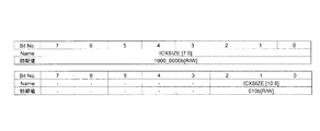
- FIG. 28 is a detailed table of fog image correction and image enhancement effective X direction size setting register ICXSIZE.
- IDX_ADDRESS is 1Ch and 1Dh.
- ICXSIZE [10: 0] sets the size (number of pixels) in the X direction of the effective area of fog image correction and image enhancement correction. An even number may be set. Can be set from 320 to XSIZE.
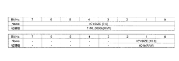
- FIG. 29 is a detailed table of fog image correction and image enhancement effective Y-direction size setting register ICYSIZE.
- IDX_ADDRESS is 1Eh and 1Fh.
- ICYSIZE [10: 0] sets the size (number of pixels) in the Y direction of the effective area of fog image correction and image enhancement correction. It can be set from 240 to YSIZE.
- FIG. 30 is a schematic diagram showing the effective range of fog image correction and image enhancement correction.
- FIG. 31 is a detailed table of the pre-gamma setting register PREGAMMA.
- IDX_ADDRESS is 20h.
- This IC has a built-in pre-gamma filter.
- This pre-gamma filter has 15 types of setting values, and the setting values are selected by PREG [3: 0].
- PREG [3: 0] can be set from “0" to "14". The lower the number, the greater the increase in the low luminance area. Note that setting “15” as PREG [3: 0] is prohibited.
- FIG. 32 is a detailed table of the brightness correction strength setting register STRENGTH.
- IDX_ADDRESS is 21h.
- STR [6: 0] sets the strength of image enhancement correction.
- STR [6: 0] can be set to a value between "0" and "127".
- FIG. 33 is a detailed table of the color difference correction intensity setting register UV_STRENGTH. IDX_ADDRESS is 22h.
- UV_STR [3: 0] sets the correction strength for image enhancement correction for color difference components.
- V_ENHANCE [3: 0] is more reddish as the number increases. + About 3% x set number is emphasized. "0" to "15" can be set.
- FIG. 34 is a detailed table of the noise suppression setting register NOISE_SUP.
- IDX_ADDRESS is 23h.
- NOISE_SUP [6: 0] sets the noise suppression value. "10” to “127” can be set. Increasing the value suppresses noise. “0” to “9” are prohibited.
- FIG. 35 is a detailed table of the edge enhancement filter setting register EDG_CNT. IDX_ADDRESS is 24h.
- EDG_ST [3: 0] sets the strength of the edge enhancement filter. "0" to "15" can be set. As the value is increased, the edge enhancement becomes stronger.
- EDG_EN sets the enable of the edge enhancement filter. The settings are as follows. “0”: Disable “1”: Enable
- FIG. 36 is a detailed table of the response time setting register RESP_SET.
- IDX_ADDRESS is 25h.
- RESP_SET sets the response time for the image enhancement effect. "0" is the earliest and “15" is the slowest.
- FIG. 37 is a detailed table of the post filter enable register PFLT_EN.
- IDX_ADDRESS is 26h.
- POFLT_EN sets the output gamma filter enable. The characteristic set in the output gamma characteristic register is used. A gamma filter is applied to the image after the image enhancement correction processing. The settings are as follows. “0": Disable “1”: Enable
- FIG. 38 is a detailed table of the output gamma characteristic registers POFLT0 to POFLT8.
- IDX_ADDRESS is 27h-2F.
- POFLT0 to POFLT8 each set an output gamma characteristic.
- FIG. 39 is a diagram showing output gamma characteristics.
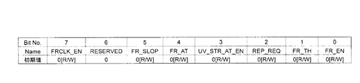
- FIG. 40 is a detailed table of the fog image correction control register FRCTL. IDX_ADDRESS is 30h.
- FRCLK_EN supplies a clock to the fog image correction block.
- the settings are as follows. "0": Clock stop "1": Clock supply
- the slope width always changes by ⁇ 1 at the SCRVADJ setting value.
- FR_AT sets the fog image correction method.
- this IC controls the FR_EN bit.
- the settings are as follows. “0”: Set fog image correction manually. “1”: Automatic fog image correction. (This IC controls it.)
- UV_STR_AT_EN is either UV_STR (IDX_ADDRESS: 22h [3: 0]) or UV_STR_AT (IDX_ADDRESS: 07h [3: 0]) as the UV_STR setting of the image enhancement correction function when automatic control is ON and the fog image correction function is enabled. Select whether to enable the setting.
- the settings are as follows. "0": Always set value of UV_STR is valid. "1”: Set value of UV_STR_AT is valid when automatic control is ON and fog image correction function is valid.
- FR_TH controls the through operation of the fog image correction block.
- the synchronization signal and data are output with the same number of cycles as in the fog image correction process being delayed.
- FR_TH may be set to “1”.
- FIG. 41 is a detailed table of the fog image correction S curve range adjustment register SCRVADJ.
- IDX_ADDRESS is 31h.
- SCRVADJ [3: 0] adjusts the S curve range for fog image correction and sets the strength of fog image correction.
- FIG. 42 is a table showing the relationship between the set value of SCRVADJ and the intensity of fog image correction.
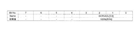
- FIG. 43 is a detailed table of the fog image correction ⁇ curve range adjustment register GCRVADJ.
- IDX_ADDRESS is 32h.
- GCRVADJ [3: 0] adjusts the ⁇ curve range for fog image correction and sets an offset of the ⁇ value.
- FIG. 44 is a table showing the relationship between the set value of GCRVADJ and the offset of the ⁇ value.
- FIG. 45 is a detailed table of the histogram average luminance value register HAVGLUM.
- IDX_ADDRESS is 36h.
- HAVGLUM [3: 0] can read the average value of the histogram. The range is from “0" to "255".
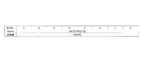
- FIG. 46 is a detailed table of the histogram standard variance register HSTDVRC.
- IDX_ADDRESS is 37h.
- HSTDVRC [3: 0] can read the variance value of the histogram.
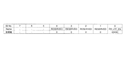
- FIG. 47 is a detailed table of the inter-field Low Pass Filter control register FR_LPF_CNT. IDX_ADDRESS is 3Eh. FR_LPF_EN enables a 5-tap Low Pass Filter for a parameter calculated in the fog image correction block. The settings are as follows. Note that writing "1" to the RESERVED bit is prohibited. "0": Low Pass Filter OFF "1": Low Pass Filter ON
- FR_LPF_COEF0 + FR_LPF_COEF1 + FR_LPF_COEF2 + FR_LPF _COEF3 + FR_LPF_COEF4 80h
- FIG. 49 is a detailed table of the automatic control UV_STR adjustment register UV_STR_AT.
- IDX_ADDRESS is 07h.
- FIG. 50 is a detailed table of automatic control variance value threshold setting registers ACVRCTH1 to ACVRCTH3.
- IDX_ADDRESS is from 08h to 0Ah.
- ACVRCTH1,2,3 [7: 0] determines whether the input image is a fog image using ACVRCTH1, ACVRCTH2, and ACVRCTH3 with respect to the variance value of the input histogram. Details will be described later with reference to FIGS. 53 and 54. Note that ACVRCTH1, ACVRCTH2, and ACVRCTH3 should be set to satisfy the following relationship.
- FIG. 51 is a detailed table of automatic control average value threshold setting registers ACAVGTH1, ACAVGTH2.
- IDX_ADDRESS is 0Bh, 0Ch.
- ACAVGTH1,2 [7: 0] is determined to be a fog image when the average luminance value of the histogram is greater than ACAVGTH1, and the correction function is enabled. If the average brightness value of the histogram becomes smaller than ACAVGTH2 after the fog image correction function is enabled, the fog image correction function is disabled. Details will be described later with reference to FIGS. 53 and 54.
- ACAVGTH1 and ACAVGTH2 should be set to satisfy the following relationship.
- ACAVGTH1 ACAVGTH2
- the hysteresis function for determining the input image luminance value is turned OFF.
- FIG. 52 is a detailed table of the automatic control S-curve correction area setting registers ACSCV11 to ACSCV13.
- IDX_ADDRESS is 0Dh to 0Fh.
- ACSCV_ULIM [3: 0], ACSCV_MH [3: 0], ACSCV_MM [3: 0], ACSCV_ML [3: 0] and ACSCV_LLIM [3: 0] Image processing correction amount: Set the S curve range adjustment. The strength of the setting value is the same as that of the SCRVADJ register (IDX_ADDRESS: 31h). Details will be described later with reference to FIGS. 53 and 54.
- ACSCV_ULIM, ACSCV_MH, ACSCV_MM, ACSCV_ML, and ACSCV_LLIM should be set to satisfy the following two relationships.
- FR_SLOP_CNT [1: 0] sets the slope time when slope setting (FR_SLOP) is enabled by automatic control.
- the settings are as follows. "00b”: Update every field "01b”: Update every 16 fields "10b”: Update every 32 fields "11b”: Update every 64 fields
- FIG. 53 is a flowchart for explaining the fog image correction automatic control
- FIG. 54 is a diagram showing an outline of the fog image correction automatic control algorithm. 53 and 54 correspond to FIGS. 4 and 6A, respectively, and therefore only the outline thereof will be described below.
- step S201 the average luminance value of the input image is compared with the ACVRCTH1 register value. If the average luminance of the input image is higher, the process proceeds to the S curve range adjustment determination state (step S202).
- a hysteresis width can be set to prevent ON / OFF near the ACVRCTH1 register value.
- the fog image correction is turned on when the input luminance is larger than the ACVRCTH1 register value, and is turned off when the input luminance is smaller than the ACVRCTH2 register value.
- the S-curve range adjustment determines the variance value of the input image and calculates the SCRVADJ register value according to the variance value.
- the setting range for S-curve range adjustment is designated by ACSCV_ULIM, ACSCV_MH, ACSCV_MM, ACSCV_ML, and ACSCV_LLIM.
- the standard dispersion range is designated by ACVRCTH1, ACVRCTH2, and ACVRCTH3, and the ACVRCTH1 and ACVRCTH2 are equally divided into four. For example, if the input variance value is the same as AVCRCTH1, the SCRVADJ register value is set to the ACSCV_ULIM value.
- the S curve range adjustment also has hysteresis as shown in FIG. 54 in order to prevent flickering at the setting boundary.
- the S curve range adjustment is performed along the path indicated by the broken line in FIG. 54, and the fog image correction function is turned off when the variance value of the input data exceeds AVCRCTH3.
- the fog image correction function is turned ON, and the S curve range is adjusted according to the variance value.
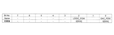
- FIG. 55 is a detailed table of the TV encoder reset register PWD. IDX_ADDRESS is 41h.
- DAC_POW turns on / off the built-in DAC operation.
- the settings are as follows. “0”: DAC operation ON “1”: DAC operation OFF
- LOGIC_POW performs clock ON / OFF control of the TV-Encoder block.
- the settings are as follows. “0”: Internal clock is turned off. “1”: Turns on the internal clock.
- FIG. 56 is a detailed table of the TV encoder display mode register DISP. IDX_ADDRESS is 43h.
- LEVEL selects whether the input data range of the TV encoder built in the IC is the full range or the ITU-R 601 range.
- DISP0 selects the operation mode of the TV encoder in the IC.
- square pixel mode 640 pixels in the horizontal direction are expanded to 720 pixels. If the clock input is other than 27MHz, you should write "0" to this bit.
- the settings are as follows. "0”: Equivalent pixel mode "1”: Square pixel mode
- FIG. 57 is a detailed table of the TV encoder video mode register VIDEO. IDX_ADDRESS is 45h.
- NTPAL selects the video output mode of the TV encoder built in this IC.
- the settings are as follows. "0": NTSC "1”: PAL
- Q_FSC selects the clock operation mode of the TV encoder in the IC. What is necessary is just to input the clock of the selected mode.
- the settings are as follows. “0”: 27 MHz clock operation "1”: 4 fsc clock operation (clock input is 8 fsc)
- PAL28 is turned on ("1") when the clock operation mode of the TV encoder in this IC is PAL and 28.375 MHz.
- the settings are as follows. “0”: When 28.375 MHz clock is not operating with PAL “1”: When 28.375 MHz clock is operating with PAL
- 510H selects the operation mode of the TV encoder in the IC.
- the settings are as follows. "0": Normal operation "1”: 510H mode
- C_OFF turns off the output of Cb, Cr and color burst signals.
- the settings are as follows. Note that “0” should be written in the RESERVED bit. “0”: Normal operation (Cb, Cr and color burst signals are added together and output.) “1”: Cb, Cr, and color burst signals are output without being added.
- FIG. 58 is a list showing usable settings of the TV encoder video mode register VIDEO. Settings not shown in this figure are prohibited.
- FIG. 59 is a detailed table of the TV encoder video mode register CVBS. IDX_ADDRESS is 46h.
- CVBS_OUT selects ON / OFF of the video output (DAC) of the TV encoder built in the IC.
- the settings are as follows. “0”: DAC output is not performed. “1”: CVBS (composite video signal) is output as the DAC output.
- IMAGE_OUT [1: 0] selects video output data of the TV encoder in the IC.
- the settings are as follows. "00b”: RESERVED “01b”: The color selected in the BGCOL register is output in the entire screen range. "10b”: RESERVED “11b”: Video is output. The color selected by BGCOL is output to the background area.
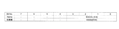
- FIG. 60 is a detailed table of the background color register BGCOL.
- IDX_ADDRESS is 47h.
- BGCOL [3: 0] selects the background color of the video output (DAC) of the TV encoder built in the IC.
- the settings are as follows. Settings other than the following are prohibited. "00 (hex)”: BLUE background color [Default] "01 (hex)”: BLACK background color "02 (hex)”: RED background color "03 (hex)”: GREEN background color "04 (hex)”: YELLOW background color "05 (hex)”: CYAN background color "06 (hex)”: MAGENTA background color "07 (hex)”: GRAY background color "08 (hex)”: WHITE background color
- FIG. 61 is a detailed table of a TV encoder color bar test register COLBAR.
- IDX_ADDRESS is 48h.
- COLBAR makes the output of the TV encoder built in this IC a color bar output. The settings are as follows. “0”: Output the input data of this IC “1”: Force color bar
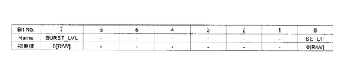
- FIG. 62 is a detailed table of the TV encoder setup register SETUP. IDX_ADDRESS is 55h.
- BURST_LVL can adjust the level of the burst signal and the color carrier wave.
- the settings are as follows. “0”: Default setting “1”: Amplifies the level of burst signal and color carrier by about 0.8 IRE against “0” setting.
- SETUP is set according to NTSC or PAL.
- the settings are as follows. “0”: For NTSC, “0” should be set. “1”: In case of PAL, “1” should be set.
- FIG. 63 is a detailed table of a TV encoder setup 2 register SETUP2.
- IDX_ADDRESS is 50h.
- SETUP2 sets the TV encoder operation mode. Settings other than the following are prohibited. “000b”: When not in 510H mode, “000b” should be set. “011b”: In the 510H mode, “011b” should be set.
- FIG. 64 is a detailed table of TV encoder gamma correction registers GM_A0 to GM_A2, GM_X0 to GM_X3, and GM_Y0 to GM_Y3.
- IDX_ADDRESS is D0h to DAh.
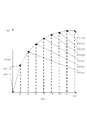
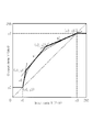
- FIG. 65 is a diagram showing a gamma correction curve. The gamma correction curve is set with the coordinates (x0, y0), (x1, y1), (x2, y2), (x3, y3) of the four points shown in FIG. 65, and three inclination coefficients a0, a1, a2 Determined by.
- the upper 4 bits are integers, and the lower 4 bits are below the decimal point.
- FIG. 66 is a table showing a setting example of the gamma collection registers GM_A0 to GM_A2, GM_X0 to GM_X3, and GM_Y0 to GM_Y3.
- the output value 16 (10h) corresponds to 0IRE
- 235 (EBh) corresponds to 100IRE.
- the maximum output is limited to 235 (EBh)
- the white level of the TV output is limited to 100 IRE.
- FIG. 67 is a detailed table of the input valid start pixel offset setting register OFS.
- IDX_ADDRESS is E0h, E1h. This register sets the effective data start pixel from HSYNC at the input, whereas H_POS is the display offset at the time of TV encoder output.
- FIG. 68 is a detailed table of a TV encoder effective data width setting register WID_VD.
- IDX_ADDRESS is E2h, E3h. This register sets the number of valid pixels in the horizontal line. The initial value is 320 pixels. The set value should be an even number. The setting range is between 100 pixels and 896 pixels. The settings are as follows. Note that the WID_VD register should be set to a multiple of four. WID_VD [1: 0]: “00b” should be written in these 2 bits.
- WID_VD [9: 0]: 000 (hex) to 063 (hex): Setting prohibited 064 (hex): 100 pixels
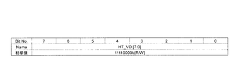
- FIG. 69 is a detailed table of a TV encoder effective line width setting register HT_VD.
- IDX_ADDRESS is E4h. This register sets the number of valid lines in the field. The initial value is 240. The number of lines actually output to the TV is a value with a +64 offset relative to the HT_VD register. The range of values that can be set in the register is from 100 to 254 lines. Therefore, the TV number displayable line number setting range is from 164 lines to 318 lines.
- the settings are as follows. HT_VD [0]: “0” should be written to this bit. HT_VD [7: 0]: 00 (HEX) to 63 (HEX): Setting prohibited 64 (HEX): 164lines
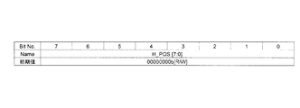
- FIG. 70 is a detailed table of the TV encoder horizontal display position offset register H_POS.
- IDX_ADDRESS is E5h. This register sets the offset of the horizontal display position within the line. The initial value is 0. The range that can be set is 0 to 504 pixels. The offset of the displayed horizontal position is expressed by the following formula. Display horizontal position offset value: H_POS [7: 0] x 2 [Pixel]
- H_POS [1: 0]: “00b” should be written to these 2 bits.
- FIG. 71 is a detailed table of a TV encoder vertical display position offset register V_POS.
- IDX_ADDRESS is E6h. This register sets the offset of the vertical display position within the field. The initial value is 0. The range that can be set is 0 to 120 lines.
- the offset of the displayed vertical position is expressed by the following formula. Display vertical position offset value: V_POS [7: 0] +4 (line in a field) (For NTSC) Display vertical position offset value: V_POS [7: 0] +23 (line in a field) (For PAL)
- V_POS The setting contents of the TV encoder vertical display position offset register V_POS are as follows.
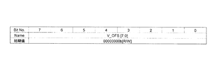
- FIG. 72 is a detailed table of an input valid start line offset setting register V_OFS.
- IDX_ADDRESS is E7h. This register sets a valid data start line from VSYNC at the input, whereas V_POS is a display offset at the time of TV encoder output.
- FIG. 73 is a schematic diagram showing the setting contents of the display position change register.
- FIG. 74 is a detailed table of the SPI control register SPICNT.
- IDX_ADDRESS is F0h.
- This register is a register that performs SPI control.
- REG_WPB sets the output level of the WPB terminal (the output value is directly reflected).
- REG_SCEB sets the output level of the SCEB terminal (output value is directly reflected).
- REG_SCK sets the output level of the SCK pin before the SPI operation (the output value is directly reflected).
- REG_SDO sets the output level of the SDO pin before the SPI operation (the output value is reflected directly).
- SWRITE is a WDATA output enable bit to the SDO terminal during SPI operation. When SWRITE is set to "0", the value of the REG_SDO bit remains output.
- SACT For SBUSY, “1” is read during the SPI operation, and “0” is read when the SPI operation is completed. SACT is write-only, and only “0” is read. Also, writing "1" to SACT generates a clock for 8-bit data and executes the SPI operation.
- FIG. 75 is a detailed table of the SPI operation clock dividing register SPIDIV.
- FIG. 76 is a detailed table of the SPI write data setting register SPIWDATA.
- IDX_ADDRESS is F2h. This register sets the output data to the SDO pin during SPI operation.
- FIG. 77 is a detailed table of the SPI read data register SPIRDATA.
- IDX_ADDRESS is F3h. This register stores input data from the SDI terminal during SPI operation.
- SPI EEPROM read address setting register 0 SPIADR0L.
- IDX_ADDRESS is F4h. This register sets the lower 8 bits of the EEPROM address when EEPROM auto read is executed when the MODE0 and MODE1 pins are "0" and "0", respectively.
- SPI EEPROM read address setting register 1 SPIADR1L.
- IDX_ADDRESS is F5h. This register sets the lower 8 bits of the EEPROM address when EEPROM auto-read is executed when the MODE0 and MODE1 pins are "1" and "0", respectively.
- Fig. 80 is a detailed table of SPI EEPROM read address setting register 2: SPIADR2L. IDX_ADDRESS is F6h. This register sets the lower 8 bits of the EEPROM address when EEPROM auto-read is executed when the MODE0 and MODE1 pins are "0" and "1", respectively.
- FIG. 81 is a detailed table of SPI EEPROM read address setting register 3: SPIADR3L. IDX_ADDRESS is F7h. This register sets the lower 8 bits of the EEPROM address when EEPROM auto-read is executed when the MODE0 and MODE1 pins are "1" and "1", respectively.
- FIG. 82 is a detailed table of an SPI EEPROM read address bit 8 setting register: SPIADR1_H. IDX_ADDRESS is F8h. The contents of this register are as follows. SPIADR0H: Set bit 8 of SPIADR0 with the EEPROM read address. SPIADR1H: Set bit 8 of SPIADR1 by EEPROM read address. SPIADR2H: Set bit 8 of SPIADR2 by EEPROM read address. SPIADR3H: Set SPIADR3 bit 8 by EEPROM read address.
- FIG. 83 is a detailed table of the initialization register SRST.
- IDX_ADDRESS is FFh.
- This register is a software reset register. The corresponding block is reset by writing "1". Only writing "1" is valid. It should not be accessed for 100ns after software reset. There is no need to reset the software after a hardware reset.
- the contents of this register are as follows.
- SRST_AIE Write “1” to reset the image enhancement block. The reset is canceled by writing "0”.
- SRST_TVE Resets the TV encoder block by writing "1". The reset is canceled by writing "0".
- SRST_REG The register is reset by writing "1". The register will have the initial value. Reset is automatically canceled.
- SRST_FOG The fog image correction block is reset by writing "1". The reset is canceled by writing "0".
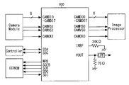
- FIG. 84 is a connection diagram illustrating an example of a system using the image processing IC 100. As shown in the figure, a camera module, a controller, an EEPROM, an image processor, and the like are connected to the outside of the image processing IC 100.
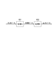
- FIG. 85A is a block diagram illustrating an example of an image correction processing apparatus having only the first image correction processing unit.
- the first image correction processing unit 601 generates digital output image data by performing a first image correction process on the digital input image data.
- the first image correction process is an image correction process based on a luminance histogram, and separately from the original purpose, the balance of color components may be lost, or the luminance dynamic range may be deficient.
- the fog image correction process described above corresponds to the above-described image correction process.
- the color component is out of balance, or the original purpose (for example, removal of fog and haze) is lost. Insufficient luminance dynamic range may occur as a result, and an unnatural output image may be generated.
- FIG. 85B is a block diagram illustrating an example of an image correction processing apparatus having a second image correction processing unit in the subsequent stage of the first image correction processing unit.
- the first image correction processing unit 601 generates digital intermediate image data by performing a first image correction process on the digital input image data.
- the first image correction process is an image correction process based on a luminance histogram as described above, and separately from the original purpose, the balance of color components is lost, or the lack of the luminance dynamic range is secondary.
- This is an image correction process that may be incurred, and corresponds to, for example, the fog image correction process described above. That is, the first image correction processing unit 601 depicted in FIG. 85B corresponds to the first image correction processing unit 201 depicted in FIG.
- the content of the first image correction process is not limited to the fog image correction process.
- the second image correction processing unit 602 performs the second image correction process on the digital intermediate image data input from the first image correction processing unit 601, thereby converting the digital output image data.
- the second image correction process refers to an image correction process for resolving the balance of color components caused by the first image correction process or the lack of the luminance dynamic range.
- This corresponds to enhancement processing (luminance dynamic range correction processing with color space correction processing such as saturation suppression). That is, the second image correction processing unit 602 depicted in FIG. 85B corresponds to the second image correction processing unit 202 depicted in FIG.
- the content of the second image correction process is not limited to the image enhancement process.
- the intermediate image data obtained by the first image correction process is finally subjected to the second image correction process for eliminating the color component imbalance and the lack of the luminance dynamic range, thereby finally It becomes possible to improve the visibility of the output image obtained.
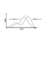
- a brightness histogram distribution is created, and brightness histogram optimization (fog and haze removal) is performed based on the maximum value, minimum value, median value, standard deviation value, etc. of the distribution. Done. As a result, good evaluation results can be obtained in most scenes of still images and moving images.
- the fog image correction amount changes for each frame, and thus the above-described minute variation may be emphasized by the fog image correction processing.
- FIG. 87 a clear difference for each frame appears in the entire luminance histogram distribution (particularly the luminance peak value) after the fog image correction processing, and there is a possibility that the screen flickers.
- fog image correction processing is performed using the entire range of the luminance histogram (that is, all luminance ranges including the vicinity of the maximum value and the minimum value of the luminance histogram that are likely to cause minute changes). Is considered to be the cause.
- the first image correction processing unit (the first image correction processing unit 201 depicted in FIG. 7 or the one depicted in FIG. 85B).
- the first image correction processing unit 601 corresponds to this), and the effective luminance range of the luminance histogram referred to when calculating the correction coefficient is variably set.
- FIG. 88 is a block diagram illustrating a first configuration example of the first image correction processing unit.
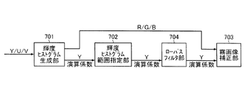
- the first image correction processing unit in this configuration example includes a luminance histogram generation unit 701, a luminance histogram range designation unit 702, and a fog image correction unit 703.
- symbol Y in a figure has shown the luminance component
- symbols U and V have shown the color component.
- symbols R, G, and B in the figure indicate a red component, a green component, and a blue component, respectively.
- the luminance histogram generation unit 701 generates a luminance histogram distribution based on the luminance component Y of the input image data, and outputs this to the luminance histogram range designation unit 702.
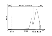
- the luminance histogram range designation unit 702 sets an effective range of the luminance histogram distribution generated by the luminance histogram generation unit 701. For example, as shown in FIG. 89, the luminance histogram range specifying unit 702 performs the calculation for the predetermined luminance range from the upper limit value (255) and the lower limit value (0) of the luminance histogram during the calculation process in the fog image correction unit 703. In order not to consider this as invalid, the maximum value and minimum value of the luminance histogram distribution are set in the register.
- the fog image correction unit 703 calculates a calculation coefficient (correction coefficient) of fog image correction processing based on the luminance histogram distribution within the effective range determined by the luminance histogram range specification unit 702, and uses this to calculate input image data The fog image correction process is performed on the.
- input image data converted from the YUV format to the RGB format is input to the fog image correction unit 703.
- the effective range of the luminance histogram distribution may be adjusted as appropriate.
- FIG. 90 is a block diagram illustrating a second configuration example of the first image correction processing unit.
- the first image correction processing unit in the present configuration example includes a low-pass filter unit 704 at the subsequent stage of the luminance histogram range specifying unit 702.
- the low-pass filter unit 704 uses the correction coefficient of the frame and the correction coefficient of at least one frame input before and after the frame, It is an inter-frame filter (inter-field filter) that performs low-pass filter processing on the correction coefficient.
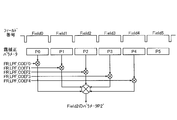
- the low-pass filter unit 704 has a function of cutting a high-frequency component (abrupt change) of the calculation parameter by performing a 5-tap low-pass filter process on the calculation parameter (fog correction parameter) inside the fog image correction block of the IC. It has.
- the fog image correction calculation parameter changes suddenly due to a sudden change in the scene of the captured image, the correction image does not immediately reflect the parameter, but changes slowly over five fields. .
- the calculation parameter is smoothed by the low-pass filter processing unit 704, thereby suppressing flickering. Can do.
- the filtering process of the calculation parameter in the low-pass filter unit 704 is executed on a field basis. Low-pass filter processing is performed using two fields before and after the field to be calculated.
- 91A and 91B are schematic diagrams for explaining the low-pass filter processing. 91A shows how to calculate the calculation parameter for field 2, and FIG. 91B shows how to calculate the calculation parameter for field 3.
- FR_LPF_COEF0 Coefficient setting for field (N-2) parameter FR_LPF_COEF1: Coefficient setting for field (N-1) parameter FR_LPF_COEF2: Coefficient setting for field N (field to be calculated) FR_LPF_COEF3: Field (N + 1) Coefficient setting for the parameter of FR_LPF_COEF4: Coefficient setting for the parameter of field (N + 2)
- Each coefficient register is composed of 8 bits, and may be expressed by an integer part: 1 bit (MSB) and a decimal part: 7 bits. Accordingly, the coefficient values for each register value (hexadecimal notation) are as follows.
- the coefficient value 0.75 when expressed in hexadecimal, it becomes 60h.
- the set value of each coefficient register must be set to 00h to 80h, and the total of the five registers should be set to 80h. This is because the sum of the coefficients needs to be 1.00.
- the strength of the low-pass filter processing decreases as the coefficient of the field to be calculated, that is, the set value of FR_LPF_COEF2 increases, and conversely increases as the set value of FR_LPF_COEF2 decreases (the coefficient value of the preceding and following fields increases).
- the parameter of the field 2 becomes the parameter after the low-pass filter processing as it is, so that the low-pass filter function is effectively turned off.
- the operation is similar.
- FR_LPF_COEF0 00h
- FR_LPF_COEF1 00h
- FR_LPF_COEF2 80h
- FR_LPF_COEF3 00h
- FR_LPF_COEF4 00h
- FR_LPF_COEF0 10h
- FR_LPF_COEF1 20h
- FR_LPF_COEF2 20h
- FR_LPF_COEF3 20h
- FR_LPF_COEF4 10h
- FR_LPF_COEF0 08h
- FR_LPF_COEF1 18h
- FR_LPF_COEF2 40h
- FR_LPF_COEF3 18h
- FR_LPF_COEF4 08h
- the image processing IC 100 includes a first external terminal CAMDI [7: 0] to which digital input image data is input from the outside of the IC; An image correction processing circuit 200 that performs predetermined image correction processing on the image data to generate digital output image data; a second external terminal CAMDO [7: 0] that outputs the digital output image data outside the IC; An encoder circuit 300 that converts the output image data in the digital format into output image data in the analog composite video format; and a third external terminal VOUT that outputs the output image data in the analog composite video format outside the IC; Is integrated.
- CAMDI [7: 0]
- An image correction processing circuit 200 that performs predetermined image correction processing on the image data to generate digital output image data
- a second external terminal CAMDO [7: 0] that outputs the digital output image data outside the IC
- An encoder circuit 300 that converts the output image data in the digital format into output image data in the analog composite video format
- a third external terminal VOUT that outputs the output image
- FIG. 92A and FIG. 92B are block diagrams each showing a configuration example of an electronic device (an indoor / outdoor surveillance camera, a network camera (IP camera), a Web camera, an in-vehicle camera, an interphone, etc.) equipped with the image processing IC according to the present invention. It is.
- an electronic device an indoor / outdoor surveillance camera, a network camera (IP camera), a Web camera, an in-vehicle camera, an interphone, etc.
- Both electronic devices 800 of both configuration examples include a camera 801, an AFE [Analog Front End] 802, a camera DSP 803, and an image processing IC 804 according to the present invention.
- FIG. 92A shows a configuration in which the image processing IC 804 is controlled by a program stored in the EEPROM 805.
- the camera 801 and the AFE 802 are controlled via a camera DSP 803 connected to a general-purpose interface (GPIO).
- FIG. 92B shows a configuration in which the image processing IC 804 is controlled by an instruction from the microcomputer 806 connected to the general-purpose interface (GPIO).
- the camera 801 and the AFE 802 are also controlled via the microcomputer 806.
- an appropriate image correction process is performed on the input image data without significantly changing the design of the existing circuit. Or analog composite video output.
- the present invention is useful for improving the visibility of an output image in an image correction processing circuit that performs various image correction processes on an input image to generate a desired output image and a semiconductor device in which the input image is integrated.
- the image correction apparatus can be used for all electronic devices that handle image data (indoor / outdoor surveillance cameras, security cameras, network cameras (IP cameras), Web cameras, in-vehicle cameras, drive recorders, intercoms, etc.). Technology.
- Image processing IC semiconductor device
- DESCRIPTION OF SYMBOLS 11 Fog image correction
- amendment part 12 Luminance histogram calculating part 13 Correction
- amendment control part 131 1st comparison part 132 2nd comparison part 133 Judgment part 14 Register
- Image source imaging device etc.
- Display devices liquid crystal display, etc.
- Microcomputer 100 Image processing IC (semiconductor device) 200 Image correction processing circuit 201 First image correction processing unit (fog image correction unit) 202 Second image correction processing unit 202a Color correction unit 202b Luminance discrimination unit 202c Image enhancement unit 202d Arithmetic processing unit 300 Encoder circuit 301 Memory controller 302 Line memory 303 Complementing unit 304 Gamma correction unit 305 Low-pass filter unit 306 Trap filter unit 307, 308 Low-pass filter unit 309 to 312 Operation processing unit 313 Digital / analog conversion unit 314 Timing signal generation unit 315 Subcarrier signal generation unit 316 Color bar signal generation unit 400 First
Landscapes
- Engineering & Computer Science (AREA)
- Multimedia (AREA)
- Signal Processing (AREA)
- Physics & Mathematics (AREA)
- General Physics & Mathematics (AREA)
- Theoretical Computer Science (AREA)
- Facsimile Image Signal Circuits (AREA)
- Image Processing (AREA)
- Studio Devices (AREA)
- Picture Signal Circuits (AREA)
Abstract
Description
従来より、デジタル画像を取り扱うデバイスないしシステム(屋内外監視カメラ、ネットワークカメラ(IPカメラ)、Webカメラ、インターホンなど)の分野では、入力画像に種々の画像補正処理(霧消し補正処理、逆光補正処理、明暗補正処理など)を施すことにより、所望の出力画像を生成する画像補正処理回路が用いられている。
図93A及び図93Bはいずれも画像データを取り扱う電子機器(屋内外監視カメラ、ネットワークカメラ(IPカメラ)、Webカメラ、車載カメラ、インターホンなど)の一従来例を示すブロック図である。
確かに、画像補正処理回路を用いれば、霧が掛かった入力画像や逆光の入力画像をより視認性の高い出力画像に変換し、これを表示デバイスに送出することが可能となる。
しかしながら、上記従来の電子機器900には、霧や靄の掛かった視認性の低い入力画像データがカメラ901で得られた場合、その入力画像データに対して適切な画像補正処理(霧消し処理)を施す手段が設けられていなかった。
上記第1の目的を達成するために、本明細書中に開示されている画像補正処理回路は、入力画像に所定の画像補正処理を施して出力画像を生成する画像補正部と;前記入力画像の1フィールド毎に輝度ヒストグラムを取得し、その平均輝度値、標準偏差値、及び、中間値のいずれか2値ないしは3値全てを算出する演算部と;前記演算部で算出された前記輝度ヒストグラムの平均輝度値、標準偏差値、及び、中間値のいずれか2値ないしは3値全てに基づいて、前記入力画像に対する画像補正処理の要否や補正量を判定し、前記画像補正部の制御を行う補正制御部と;を有して成る構成(第1-1の構成)とされている。
上記第2の目的を達するために、本明細書中に開示されている画像補正処理装置は、装置外部からデジタル形式の入力画像データが入力される第1の外部端子と;前記デジタル形式の入力画像データに所定の画像補正処理を施してデジタル形式の出力画像データを生成する画像補正処理回路と;装置外部に前記デジタル形式の出力画像データを出力する第2の外部端子と;前記デジタル形式の出力画像データをアナログコンポジットビデオ形式の出力画像データに変換するエンコーダ回路と;装置外部に前記アナログコンポジットビデオ形式の出力画像データを出力する第3の外部端子と;を集積化して成る構成(第2-1の構成)とされている。
される。
REG_SCEB:SCEBピンの論理を指定する。レジスタ値がそのままSCEBピンに
出力される。
SWDATA[7:0]:EEPROMへの書き込みデータを指定する。MSBファーストで転
送される。
SRDATA[7:0]:EEPROMからのデータを読み出せる。MSBファーストとして変
換する。
[MODE1,MODE0] = [Low, Low] : ST_ADR = 000h
[MODE1,MODE0] = [Low, High] : ST_ADR = 080h
[MODE1,MODE0] = [High, Low] : ST_ADR = 100h
[MODE1,MODE0] = [High, High] : ST_ADR = 180h
S-CODE:8’b0000_0001。画像処理IC100(以下では適宜、本ICと
略称する)はこのコードを受け、以降のデータを有効なレジスタ
値と判断する。
Index:本ICの設定開始インデックスアドレス
Size:設定サイズ数(バイト)
Data:設定データ。データ数はSizeバイト
P-CODE [3:0]:4’b0100。本ICはこのコードを受け、自動読み出し機能
を停止する。
PER [3:0]:MODE0、MODE1のポーリング間隔を設定する。
"0":CAMCKIの立ち下がりエッジでデータ変化、立ち上がりエッジでデー
タ取り込み(図18Aを参照)
"1":CAMCKIの立ち上がりエッジでデータ変化、立ち下がりエッジでデー
タ取り込み(図18Bを参照)
"0":サスペンドモード解除
"1":サスペンドモード
"0":AUTO,MODE0,MODE1のそれぞれに内蔵プルダウン抵抗が接続される。
"1":AUTO,MODE0,MODE1のそれぞれから内蔵プルダウン抵抗を切り離す。
"0":画像データがデジタル端子から出力される。
"1":CAMDO0-7,CAMHSO,CAMVSO,CAMCKOはlow出力される。
"0":CAMHSOを出力
"1":FR_ENを出力
"00b":フルレンジでデータ入力/出力を行う。
"11b":ITU601レンジでデータ入力/出力を行う。
"0":Hsync , Vsync別信号
"1":ITU656フォーマット
"0":色空間変換あり
"1":色空間変換なし
"0":ディスエーブル
"1":イネーブル
"0":ディスエーブル
"1":イネーブル
"0":クロック停止
"1":クロック供給
"0":スロープ制御ディスエーブル
"1":スロープ制御イネーブル
"0":霧画像補正をマニュアル設定する。
"1":霧画像補正を自動で行う。(本ICが制御する。)
"0":常にUV_STRの設定値が有効
"1":自動制御ONかつ霧画像補正機能有効時、UV_STR_ATの設定値が有
効
"1":取り込み未(36h、37hのデータ無効)
"0":取り込み完了(36h、37hのデータ有効)
<FR_AT="0"設定時>
"0":霧画像補正ディスエーブル
"1":霧画像補正イネーブル
<FR_AT="1"設定時>
"0":霧画像補正停止中
"1":霧画像補正動作中
"0":Low Pass Filter OFF
"1":Low Pass Filter ON
係数 = bit7*20 + bit6*2-1 + bit5*2-2 + bit4*2-3 +
・・・ + bit0*2-7
P(n)’ = P(n-2)*FR_LPF_COEF0 + P(n-1)*
FR_LPF_COEF1 + P(n)* FR_LPF_COEF2 +
P(n+1)* FR_LPF_COEF3 +P(n+2)*
FR_LPF_COEF4
FR_LPF_COEF0+FR_LPF_COEF1+FR_LPF_COEF2+FR_LPF
_COEF3+FR_LPF_COEF4 = 80h
ACVRCTH1 + 4 ≦ ACVRCTH2 < ACVRCTH3
ACAVGTH1≧ACAVGTH2
ACSCV_ULIM > ACSCV_LLIM
ACSCV_ULIM≧ACSCV_MH≧ACSCV_MM≧ACSCV_ML≧ACSCV_LLIM
"00b":毎フィールド更新
"01b":16フィールド毎更新
"10b":32フィールド毎更新
"11b":64フィールド毎更新
まず、ステップS201にて、入力画像の平均輝度値とACVRCTH1レジスタ値とを比較する。入力画像の平均輝度の方が高ければ、Sカーブレンジ調整判定ステート(ステップS202)へ移行する。輝度判定には、ACVRCTH1レジスタ値付近でのON/OFFを防ぐために、ヒステリシス幅を設定することが可能である。霧画像補正は入力輝度がACVRCTH1レジスタ値よりも大きければONし、入力輝度がACVRCTH2レジスタ値よりも小さければOFFする。
Sカーブレンジ調整は、入力画像の分散値を判定し、分散値に応じてSCRVADJレジスタ値を算出する。Sカーブレンジ調整の設定範囲指定は、ACSCV_ULIM、ACSCV_MH、ACSCV_MM、ACSCV_ML、ACSCV_LLIMにて行う。標準分散範囲指定は、ACVRCTH1、ACVRCTH2、ACVRCTH3で行い、ACVRCTH1、ACVRCTH2の間は、等分に4分割する。例えば、入力分散値がACVRCTH1と同じ値であればSCRVADJレジスタ値はACSCV_ULIM値に設定される。入力輝度判定時と同様に、Sカーブレンジ調整でも、設定境界でのちらつきを防止するため、図54に示すように、ヒステリシスを持っている。入力画像の分散値が次第に大きくなる場合には、図54の破線で示される経路でSカーブレンジ調整を行い、入力データの分散値がACVRCTH3以上になると霧画像補正機能をOFFする。一旦OFFした後は、入力データの分散値がACVRCTH2以上になれば、霧画像補正機能をONし、分散値に応じたSカーブレンジ調整を行う。
"0":DAC動作ON
"1":DAC動作OFF
"0":内部クロックをOFFする。
"1":内部クロックをONする。
"0":ITU601R = 2’b00設定の場合はLEVEL=0と設定すべきである。
"1":ITU601R = 2’b11設定の場合はLEVEL=1と設定すべきである。
"0":等価ピクセルモード
"1":スクウェアピクセルモード
"0":NTSC
"1":PAL
"0":27MHzクロック動作
"1":4fscクロック動作(クロック入力は8fsc)
"0":PALで28.375MHzクロック動作しない場合
"1":PALで28.375MHzクロック動作する場合
"0":通常動作
"1":510Hモード
"0":通常動作(Cb、Cr及びカラーバースト信号を足し合わせて出力する
。)
"1":Cb、Cr及びカラーバースト信号を足し合わせずに出力する。
"0":DAC出力は行わない。
"1":DAC出力としてCVBS(コンポジットビデオ信号)が出力される。
"00b":RESERVED
"01b":BGCOLレジスタで選んだ色が全ての画面範囲で出力される。
"10b":RESERVED
"11b":映像が出力される。また、バックグラウンドエリアにはBGCOLで
選んだ色が出力される。
"00(hex)":BLUE background color [Default]
"01(hex)":BLACK background color
"02(hex)":RED background color
"03(hex)":GREEN background color
"04(hex)":YELLOW background color
"05(hex)":CYAN background color
"06(hex)":MAGENTA background color
"07(hex)":GRAY background color
"08(hex)":WHITE background color
"0":本ICの入力データを出力
"1":強制的にカラーバーを出力
"0":Default設定
"1":"0"設定に対し、バースト信号、色搬送波のレベルを0.8IRE程度
増幅する。
"0":NTSCの場合は、"0"を設定すべきである。
"1":PALの場合には、"1"を設定すべきである。
"000b":510Hモード以外の場合は、"000b"を設定すべきである。
"011b":510Hモードの場合には、"011b"を設定すべきである。
図65は、ガンマコレクションカーブを示す図である。ガンマコレクションカーブの設定は、図65に示した4点の座標(x0,y0),(x1,y1),(x2,y2),(x3,y3)と、3つの傾き係数a0,a1,a2により決定される。3つの傾き係数a0,a1,a2に相当するビット値GM_A0,GM_A1,GM_A2は、上位4ビットが整数で、下位4ビットが少数点以下を表す。
1) X < x0の時
Y= y0
2) x0 ≦ X < x1の時
Y = a0 * (X - x0) + y0
3) x1 ≦ X < x2の時
Y = a1 * (X - x1) + y1
4) x2 ≦ X < x3の時
Y = a2 * (X - x2) + y2
5) x3 ≦ Xの時
Y = y3
WID_VD[1:0]:この2ビットには"00b"を書くべきである。
WID_VD[9:0]:000(hex)~063(hex):設定禁止
064(hex):100 pixels
|
|
140(hex):320 pixels [Default]
| ex.) At QVGA image input
|
2D0(hex):720 pixels
|
|
3F0(hex):1008 pixels
3F1(hex)~3FF(hex):設定禁止
HT_VD[0] : このビットには“0”を書くべきである。
HT_VD[7:0]: 00(HEX)~63(HEX):設定禁止
64(HEX):164lines
|
|
F0(HEX):304lines;デフォルト
|
|
FE (HEX):318lines
表示水平位置のオフセット値 : H_POS[7:0] x 2 [Pixel]
H_POS[1:0]:この2ビットには“00b”を書き込むべきである。
H_POS[7:0]:00(HEX):デフォルト位置
04(HEX):右に8ピクセルシフトした位置のスクリーン上
に表示
|
|
FC(HEX):右に504ピクセルシフトした位置のスクリーン上
に表示
FD(HEX)~FF(HEX):設定禁止
表示垂直位置のオフセット値:V_POS[7:0]+4(line in a field)
(NTSCの場合)
表示垂直位置のオフセット値:V_POS[7:0]+23(line in a field)
(PALの場合)
V_POS[1:0]:この2ビットには“00b”を書き込むべきである。
V_POS[7:0]:00(HEX):デフォルト位置
04(HEX):上に8ラインシフトした位置のスクリーン上に表
示
|
|
78(HEX):上に240ラインシフトした位置のスクリーン上に
表示
79(HEX)~7F(HEX):設定禁止
80(HEX):デフォルト位置と同じ
84(HEX):下に8ラインシフトした位置のスクリーン上に表
示
|
|
F8(HEX):下に240ラインシフトした位置のスクリーン上に
表示
F9(HEX)~FF(HEX):設定禁止
SCK周波数:1/(2^SPIPREDIV[2:0])/(SPIDIV[4:0]+1)
初期値35.5MHz/(2^4*(22+1))=96.5kHz;CAMCKI周波数が35.5MHzの時
SPIADR0H:EEPROM読み出しアドレスでSPIADR0のビット8を設定する。
SPIADR1H:EEPROM読み出しアドレスでSPIADR1のビット8を設定する。
SPIADR2H:EEPROM読み出しアドレスでSPIADR2のビット8を設定する。
SPIADR3H:EEPROM読み出しアドレスでSPIADR3のビット8を設定する。
SRST_AIE:"1"を書き込むことで、画像エンハンスブロックのリセッ
トを行う。"0"を書き込むことでリセットは解除される。
SRST_TVE:"1"を書き込むことでTVエンコーダブロックのリセットを
行う。"0"を書き込むことでリセットは解除される。
SRST_REG:"1"を書き込むことでレジスタのリセットを行う。レジス
タはイニシャルの値になる。リセットは自動的に解除される
。
SRST_FOG:"1"を書き込むことで霧画像補正ブロックのリセットを行
う。"0"を書き込むことでリセットは解除される。
FR_LPF_COEF1:フィールド(N-1)のパラメータに対する係数設定
FR_LPF_COEF2:フィールドN(演算対象となるフィールド)のパラメ
ータに対する係数設定
FR_LPF_COEF3:フィールド(N+1)のパラメータに対する係数設定
FR_LPF_COEF4:フィールド(N+2)のパラメータに対する係数設定
40h:0.5000000
20h:0.2500000
10h:0.1250000
08h:0.0625000
04h:0.0312500
02h:0.0156250
01h:0.0078125
FR_LPF_COEF1:00h
FR_LPF_COEF2:80h
FR_LPF_COEF3:00h
FR_LPF_COEF4:00h
FR_LPF_COEF0:10h
FR_LPF_COEF1:20h
FR_LPF_COEF2:20h
FR_LPF_COEF3:20h
FR_LPF_COEF4:10h
FR_LPF_COEF0:08h
FR_LPF_COEF1:18h
FR_LPF_COEF2:40h
FR_LPF_COEF3:18h
FR_LPF_COEF4:08h
11 霧画像補正部
12 輝度ヒストグラム演算部
13 補正制御部
131 第1比較部
132 第2比較部
133 判定部
14 レジスタ
20 画像ソース(撮像デバイスなど)
30 表示デバイス(液晶ディスプレイなど)
40 マイコン
100 画像処理IC(半導体装置)
200 画像補正処理回路
201 第1の画像補正処理部(霧画像補正部)
202 第2の画像補正処理部
202a カラーコレクション部
202b 輝度判別部
202c 画像エンハンス部
202d 演算処理部
300 エンコーダ回路
301 メモリコントローラ
302 ラインメモリ
303 補完部
304 ガンマ補正部
305 ローパスフィルタ部
306 トラップフィルタ部
307、308 ローパスフィルタ部
309~312 演算処理部
313 デジタル/アナログ変換部
314 タイミング信号発生部
315 サブキャリア信号発生部
316 カラーバー信号発生部
400 第1シリアルインターフェース回路(I2C)
500 第2シリアルインターフェイス回路(SPI)
601 第1の画像補正処理部
602 第2の画像補正処理部
701 輝度ヒストグラム生成部
702 輝度ヒストグラム範囲指定部
703 霧画像補正部
704 ローパスフィルタ部
800 電子機器
801 カメラ
802 AFE
803 カメラDSP
804 画像処理IC
805 EEPROM
806 マイコン
Claims (12)
- 入力画像に所定の画像補正処理を施して出力画像を生成する画像補正部と;
前記入力画像の1フィールド毎に輝度ヒストグラムを取得し、その平均輝度値、標準偏差値、及び、中間値のいずれか2値ないしは3値全てを算出する演算部と;
前記演算部で算出された前記輝度ヒストグラムの平均輝度値、標準偏差値、及び、中間値のいずれか2値ないしは3値全てに基づいて、前記入力画像に対する画像補正処理の要否や補正量を判定し、前記画像補正部の制御を行う補正制御部と;
を有して成ることを特徴とする画像補正処理回路。 - 前記画像補正部は、前記入力画像に対して霧画像補正処理を施すものであり、
前記補正制御部は、前記輝度ヒストグラムの平均輝度値と標準偏差値に基づいて、前記霧画像補正処理の要否や補正量を判定するものであることを特徴とする請求項1に記載の画像補正処理回路。 - 前記補正制御部は、前記輝度ヒストグラムの平均輝度値が第1の閾値よりも大きく、かつ、前記輝度ヒストグラムの標準偏差値が第2の閾値よりも小さいとき、前記霧画像補正処理が必要であると判定することを特徴とする請求項2に記載の画像補正処理回路。
- 前記補正制御部は、前記霧画像補正処理が必要であると判定したとき、前記輝度ヒストグラムの標準偏差値が小さいほど、前記霧画像補正処理の補正量を段階的に或いは連続的に大きく設定することを特徴とする請求項3に記載の画像補正処理回路。
- 第1の閾値、及び、第2の閾値の少なくとも一方には、ヒステリシス幅が設定されていることを特徴とする請求項3または請求項4に記載の画像補正処理回路。
- 前記入力画像に対する画像補正処理の要否や補正量を判定する際に前記補正制御部で参照される種々のパラメータを外部設定するためのレジスタを有して成ることを特徴とする請求項1~請求項5のいずれかに記載の画像補正処理回路。
- 請求項1~請求項6のいずれかに記載の画像補正処理回路を集積化して成ることを特徴とする半導体装置。
- 装置外部からデジタル形式の入力画像データが入力される第1の外部端子と;
前記デジタル形式の入力画像データに所定の画像補正処理を施してデジタル形式の出力画像データを生成する画像補正処理回路と;
装置外部に前記デジタル形式の出力画像データを出力する第2の外部端子と;
前記デジタル形式の出力画像データをアナログコンポジットビデオ形式の出力画像データに変換するエンコーダ回路と;
装置外部に前記アナログコンポジットビデオ形式の出力画像データを出力する第3の外部端子と;
を集積化して成ることを特徴とする画像補正処理装置。 - 前記画像補正処理回路は、
前記デジタル形式の入力画像データに対して、輝度ヒストグラムに基づく画像補正処理であって、本来の目的とは別に、色成分のバランス崩れ、ないしは、輝度ダイナミックレンジの不足を副次的に招くおそれのある第1の画像補正処理を施すことにより、デジタル形式の中間画像データを生成する第1の画像補正処理部と;
前記デジタル形式の中間画像データに対して、第1の画像補正処理によって生じた色成分のバランス崩れ、ないしは、輝度ダイナミックレンジの不足を解消する第2の画像補正処理を施すことにより、前記デジタル形式の出力画像データを生成する第2の画像補正処理部と;
を有して成ることを特徴とする請求項8に記載の画像補正処理装置。 - 前記第1の画像補正処理は、霧画像補正処理であり、前記第2の画像補正処理は、色補正処理、ないしは、輝度ダイナミックレンジ補正であることを特徴とする請求項9に記載の画像補正処理装置。
- 前記第1の画像補正処理部は、補正係数の算出時に参照される前記輝度ヒストグラムの有効輝度範囲が可変的に設定されることを特徴とする請求項9または請求項10に記載の画像補正処理装置。
- 前記第1の画像補正処理部は、あるフレームの補正係数を決定する際、当該フレームの補正係数と、当該フレームの前後に入力される少なくとも一のフレームの補正係数と、を用いて、当該フレームの補正係数にローパスフィルタ処理を施すことを特徴とする請求項11に記載の画像補正処理装置。
Priority Applications (2)
| Application Number | Priority Date | Filing Date | Title |
|---|---|---|---|
| US13/141,130 US8675962B2 (en) | 2008-12-22 | 2009-12-21 | Image correction processing circuit, semiconductor device, and image correction processing device |
| CN200980152089.0A CN102265594B (zh) | 2008-12-22 | 2009-12-21 | 图像修正处理电路、半导体装置、图像修正处理装置 |
Applications Claiming Priority (4)
| Application Number | Priority Date | Filing Date | Title |
|---|---|---|---|
| JP2008-325166 | 2008-12-22 | ||
| JP2008325166A JP5325562B2 (ja) | 2008-12-22 | 2008-12-22 | 画像補正処理回路及びこれを集積化して成る半導体装置 |
| JP2009269840A JP5513861B2 (ja) | 2009-11-27 | 2009-11-27 | 画像補正処理装置 |
| JP2009-269840 | 2009-11-27 |
Publications (1)
| Publication Number | Publication Date |
|---|---|
| WO2010074012A1 true WO2010074012A1 (ja) | 2010-07-01 |
Family
ID=42287621
Family Applications (1)
| Application Number | Title | Priority Date | Filing Date |
|---|---|---|---|
| PCT/JP2009/071201 Ceased WO2010074012A1 (ja) | 2008-12-22 | 2009-12-21 | 画像補正処理回路、半導体装置、画像補正処理装置 |
Country Status (3)
| Country | Link |
|---|---|
| US (1) | US8675962B2 (ja) |
| CN (1) | CN102265594B (ja) |
| WO (1) | WO2010074012A1 (ja) |
Cited By (2)
| Publication number | Priority date | Publication date | Assignee | Title |
|---|---|---|---|---|
| JP2014102743A (ja) * | 2012-11-21 | 2014-06-05 | Fujitsu Ltd | 報知制御方法、報知制御装置および報知制御プログラム |
| WO2015190184A1 (ja) * | 2014-06-12 | 2015-12-17 | Eizo株式会社 | 画像処理システム及びコンピュータ読み取り可能な記録媒体 |
Families Citing this family (15)
| Publication number | Priority date | Publication date | Assignee | Title |
|---|---|---|---|---|
| KR101754382B1 (ko) * | 2010-03-11 | 2017-07-05 | 가부시키가이샤 한도오따이 에네루기 켄큐쇼 | 반도체 장치 |
| US9355649B2 (en) | 2012-11-13 | 2016-05-31 | Adobe Systems Incorporated | Sound alignment using timing information |
| US10638221B2 (en) | 2012-11-13 | 2020-04-28 | Adobe Inc. | Time interval sound alignment |
| US10249321B2 (en) | 2012-11-20 | 2019-04-02 | Adobe Inc. | Sound rate modification |
| JP6000133B2 (ja) | 2013-01-08 | 2016-09-28 | 株式会社 日立産業制御ソリューションズ | 撮像装置、撮像システム及び撮像方法 |
| US9031345B2 (en) * | 2013-03-11 | 2015-05-12 | Adobe Systems Incorporated | Optical flow accounting for image haze |
| US9165373B2 (en) | 2013-03-11 | 2015-10-20 | Adobe Systems Incorporated | Statistics of nearest neighbor fields |
| US9129399B2 (en) | 2013-03-11 | 2015-09-08 | Adobe Systems Incorporated | Optical flow with nearest neighbor field fusion |
| US9025822B2 (en) | 2013-03-11 | 2015-05-05 | Adobe Systems Incorporated | Spatially coherent nearest neighbor fields |
| JP2015156600A (ja) | 2014-02-21 | 2015-08-27 | 株式会社 日立産業制御ソリューションズ | 画像信号処理装置,画像信号処理方法,および撮像装置 |
| JP6284408B2 (ja) * | 2014-04-03 | 2018-02-28 | オリンパス株式会社 | 画像処理装置、撮像装置、判定方法、駆動方法、撮像方法およびプログラム |
| US20160107572A1 (en) * | 2014-10-20 | 2016-04-21 | Skully Helmets | Methods and Apparatus for Integrated Forward Display of Rear-View Image and Navigation Information to Provide Enhanced Situational Awareness |
| CN107317968B (zh) * | 2017-07-27 | 2020-01-10 | Oppo广东移动通信有限公司 | 图像去雾方法、装置、计算机可存储介质和移动终端 |
| CN111882493B (zh) * | 2020-06-22 | 2024-11-12 | 浙江大华技术股份有限公司 | 图像的颜色调整方法、装置、设备和计算机可读存储介质 |
| US12299853B2 (en) * | 2021-11-12 | 2025-05-13 | Verily Life Sciences Llc | Dynamic smoke reduction in images from a surgical system |
Citations (9)
| Publication number | Priority date | Publication date | Assignee | Title |
|---|---|---|---|---|
| JPH07281633A (ja) * | 1994-04-06 | 1995-10-27 | Fujitsu General Ltd | 電子ディスプレイの映像表示処理方法およびその装置 |
| JPH0946546A (ja) * | 1995-06-21 | 1997-02-14 | Sony Electron Inc | ビデオ表示装置 |
| JP2000156797A (ja) * | 1998-11-18 | 2000-06-06 | Sony Corp | 画像処理装置及び画像処理方法 |
| JP2003169231A (ja) * | 2001-11-29 | 2003-06-13 | Ricoh Co Ltd | 画像処理装置、コンピュータ・プログラム |
| JP2004064710A (ja) * | 2002-07-31 | 2004-02-26 | Fuji Photo Film Co Ltd | 撮像装置及びディストーション補正方法 |
| JP2004120589A (ja) * | 2002-09-27 | 2004-04-15 | Canon Inc | 信号処理装置、撮像装置、信号処理方法、プログラム、及びコンピュータ読み取り可能な記憶媒体 |
| JP2006157469A (ja) * | 2004-11-30 | 2006-06-15 | Sony Corp | 画像処理装置、画像処理方法及び撮像装置 |
| JP2007036946A (ja) * | 2005-07-29 | 2007-02-08 | Toshiba Corp | 映像信号処理装置及び映像信号処理方法 |
| JP2007184888A (ja) * | 2005-12-05 | 2007-07-19 | Konica Minolta Photo Imaging Inc | 撮像装置、画像処理装置、画像処理方法、及び画像処理プログラム |
Family Cites Families (6)
| Publication number | Priority date | Publication date | Assignee | Title |
|---|---|---|---|---|
| US6014128A (en) | 1995-06-21 | 2000-01-11 | Texas Instruments Incorporated | Determining optimal pulse width modulation patterns for spatial light modulator |
| US6825884B1 (en) * | 1998-12-03 | 2004-11-30 | Olympus Corporation | Imaging processing apparatus for generating a wide dynamic range image |
| JP3981260B2 (ja) | 2001-11-13 | 2007-09-26 | オリンパス株式会社 | 階調補正装置 |
| JP2004304712A (ja) | 2003-04-01 | 2004-10-28 | Canon Inc | 画像処理方法及び装置 |
| JP4379129B2 (ja) * | 2004-01-23 | 2009-12-09 | ソニー株式会社 | 画像処理方法、および画像処理装置、並びにコンピュータ・プログラム |
| US8295346B2 (en) * | 2009-04-08 | 2012-10-23 | Samsung Electronics Co., Ltd. | Small detail reservation in content-adaptive quantization |
-
2009
- 2009-12-21 CN CN200980152089.0A patent/CN102265594B/zh not_active Expired - Fee Related
- 2009-12-21 WO PCT/JP2009/071201 patent/WO2010074012A1/ja not_active Ceased
- 2009-12-21 US US13/141,130 patent/US8675962B2/en active Active
Patent Citations (9)
| Publication number | Priority date | Publication date | Assignee | Title |
|---|---|---|---|---|
| JPH07281633A (ja) * | 1994-04-06 | 1995-10-27 | Fujitsu General Ltd | 電子ディスプレイの映像表示処理方法およびその装置 |
| JPH0946546A (ja) * | 1995-06-21 | 1997-02-14 | Sony Electron Inc | ビデオ表示装置 |
| JP2000156797A (ja) * | 1998-11-18 | 2000-06-06 | Sony Corp | 画像処理装置及び画像処理方法 |
| JP2003169231A (ja) * | 2001-11-29 | 2003-06-13 | Ricoh Co Ltd | 画像処理装置、コンピュータ・プログラム |
| JP2004064710A (ja) * | 2002-07-31 | 2004-02-26 | Fuji Photo Film Co Ltd | 撮像装置及びディストーション補正方法 |
| JP2004120589A (ja) * | 2002-09-27 | 2004-04-15 | Canon Inc | 信号処理装置、撮像装置、信号処理方法、プログラム、及びコンピュータ読み取り可能な記憶媒体 |
| JP2006157469A (ja) * | 2004-11-30 | 2006-06-15 | Sony Corp | 画像処理装置、画像処理方法及び撮像装置 |
| JP2007036946A (ja) * | 2005-07-29 | 2007-02-08 | Toshiba Corp | 映像信号処理装置及び映像信号処理方法 |
| JP2007184888A (ja) * | 2005-12-05 | 2007-07-19 | Konica Minolta Photo Imaging Inc | 撮像装置、画像処理装置、画像処理方法、及び画像処理プログラム |
Cited By (6)
| Publication number | Priority date | Publication date | Assignee | Title |
|---|---|---|---|---|
| JP2014102743A (ja) * | 2012-11-21 | 2014-06-05 | Fujitsu Ltd | 報知制御方法、報知制御装置および報知制御プログラム |
| US9524644B2 (en) | 2012-11-21 | 2016-12-20 | Fujitsu Limited | Notification control method and notification control device |
| WO2015190184A1 (ja) * | 2014-06-12 | 2015-12-17 | Eizo株式会社 | 画像処理システム及びコンピュータ読み取り可能な記録媒体 |
| JPWO2015190184A1 (ja) * | 2014-06-12 | 2017-04-20 | Eizo株式会社 | 画像処理システム及びプログラム |
| RU2654159C1 (ru) * | 2014-06-12 | 2018-05-16 | ЭЙЗО Корпорайшн | Система обработки изображений и машиночитаемый записывающий носитель |
| RU2664415C2 (ru) * | 2014-06-12 | 2018-08-17 | ЭЙЗО Корпорайшн | Система обработки изображений и машиночитаемый записывающий носитель |
Also Published As
| Publication number | Publication date |
|---|---|
| US20110261261A1 (en) | 2011-10-27 |
| CN102265594A (zh) | 2011-11-30 |
| US8675962B2 (en) | 2014-03-18 |
| CN102265594B (zh) | 2014-07-02 |
Similar Documents
| Publication | Publication Date | Title |
|---|---|---|
| WO2010074012A1 (ja) | 画像補正処理回路、半導体装置、画像補正処理装置 | |
| US7969793B2 (en) | Register configuration control device, register configuration control method, and program for implementing the method | |
| CN101076087B (zh) | 图像校正电路、图像校正方法和图像显示器 | |
| EP3306944B1 (en) | Display method and display device | |
| US7787023B2 (en) | Video signal processing apparatus | |
| US10102787B2 (en) | Image signal processing apparatus and control method therefor | |
| JP5513861B2 (ja) | 画像補正処理装置 | |
| US20090021643A1 (en) | Digital television chip, system and method thereof | |
| TW200809753A (en) | Methods and systems for LCD backlight color control | |
| US10104306B2 (en) | Image processing method applied to a display and associated circuit | |
| KR20110140081A (ko) | 화상 처리 장치, 촬상 장치, 화상 처리 방법, 및 화상 처리 프로그램 | |
| TWI650998B (zh) | 應用在機上盒的格式轉換電路及相關的方法 | |
| JPWO2009075027A1 (ja) | 輝度情報表示装置および方法 | |
| JP6190482B1 (ja) | 表示制御装置、表示装置、テレビジョン受像機、表示制御装置の制御方法、制御プログラム、及び記録媒体 | |
| US8447131B2 (en) | Image processing apparatus and image processing method | |
| JP2009116254A (ja) | 表示装置及び表示システム | |
| US20110057945A1 (en) | Video display apparatus and video display method | |
| KR101469839B1 (ko) | 이미지 센서 및 이를 포함하는 감시 시스템 | |
| US20020113947A1 (en) | Image display apparatus | |
| JP2009200762A (ja) | 画像処理回路、半導体装置、画像処理装置 | |
| JP4626533B2 (ja) | 画像処理装置およびその方法、プログラム、記録媒体 | |
| US20260064343A1 (en) | Monitors with enhanced edid information for supporting picture-mode processing in a source device | |
| US8854490B2 (en) | Method and apparatus for compensating a black level of an image signal | |
| JP5538973B2 (ja) | 撮像装置 | |
| KR100933171B1 (ko) | 그래픽 디스플레이 기능을 구현한 비메모리 반도체 |
Legal Events
| Date | Code | Title | Description |
|---|---|---|---|
| WWE | Wipo information: entry into national phase |
Ref document number: 200980152089.0 Country of ref document: CN |
|
| 121 | Ep: the epo has been informed by wipo that ep was designated in this application |
Ref document number: 09834813 Country of ref document: EP Kind code of ref document: A1 |
|
| WWE | Wipo information: entry into national phase |
Ref document number: 13141130 Country of ref document: US |
|
| NENP | Non-entry into the national phase |
Ref country code: DE |
|
| 122 | Ep: pct application non-entry in european phase |
Ref document number: 09834813 Country of ref document: EP Kind code of ref document: A1 |