WO2010067730A1 - 磁気ヘッド - Google Patents
磁気ヘッド Download PDFInfo
- Publication number
- WO2010067730A1 WO2010067730A1 PCT/JP2009/070148 JP2009070148W WO2010067730A1 WO 2010067730 A1 WO2010067730 A1 WO 2010067730A1 JP 2009070148 W JP2009070148 W JP 2009070148W WO 2010067730 A1 WO2010067730 A1 WO 2010067730A1
- Authority
- WO
- WIPO (PCT)
- Prior art keywords
- layer
- magnetoresistive
- magnetoresistive element
- intermediate layer
- magnetic
- Prior art date
- Legal status (The legal status is an assumption and is not a legal conclusion. Google has not performed a legal analysis and makes no representation as to the accuracy of the status listed.)
- Ceased
Links
Images





Classifications
-
- G—PHYSICS
- G11—INFORMATION STORAGE
- G11B—INFORMATION STORAGE BASED ON RELATIVE MOVEMENT BETWEEN RECORD CARRIER AND TRANSDUCER
- G11B5/00—Recording by magnetisation or demagnetisation of a record carrier; Reproducing by magnetic means; Record carriers therefor
- G11B5/127—Structure or manufacture of heads, e.g. inductive
- G11B5/33—Structure or manufacture of flux-sensitive heads, i.e. for reproduction only; Combination of such heads with means for recording or erasing only
- G11B5/39—Structure or manufacture of flux-sensitive heads, i.e. for reproduction only; Combination of such heads with means for recording or erasing only using magneto-resistive devices or effects
- G11B5/3903—Structure or manufacture of flux-sensitive heads, i.e. for reproduction only; Combination of such heads with means for recording or erasing only using magneto-resistive devices or effects using magnetic thin film layers or their effects, the films being part of integrated structures
- G11B5/3906—Details related to the use of magnetic thin film layers or to their effects
Definitions
- the present invention relates to a magnetic recording / reproducing head including a differential reproducing head and a recording head, and a magnetic recording / reproducing apparatus equipped with the magnetic recording / reproducing head.
- magnetic recording / reproducing apparatuses such as HDDs (Hard Disk Drives) are required to rapidly increase recording density, and magnetic heads and magnetic media are also required to achieve high recording density.
- a magnetoresistive head mounted as a reproducing element in a magnetic recording / reproducing apparatus a structure called a spin valve using a magnetoresistive effect of a multilayer film in which a ferromagnetic metal layer is laminated via a nonmagnetic metal layer is used.
- the magnetoresistive effect is a phenomenon in which the electrical resistance changes depending on the angle between the magnetizations of the two ferromagnetic layers sandwiching the intermediate layer.
- a spin valve using the magnetoresistive effect has an antiferromagnetic layer / ferromagnetic layer / non-magnetic intermediate layer / ferromagnetic layer structure, and an exchange coupling magnetic field generated at the interface of the antiferromagnetic layer / ferromagnetic layer.
- An output is obtained by substantially fixing the magnetization of the ferromagnetic layer in contact with the antiferromagnetic layer and freely rotating the magnetization of the other ferromagnetic layer by an external magnetic field.
- the antiferromagnetic layer and the ferromagnetic layer whose magnetization is substantially fixed by the antiferromagnetic layer are collectively referred to as a fixed layer, the ferromagnetic layer whose magnetization is rotated by an external magnetic field is a free layer, and the nonmagnetic intermediate layer is Called the middle layer. Resistance change is called MR (M agneto- R esistive) ratio can be increased reproduction output higher MR ratio is high.
- the spin valve using the magnetoresistive effect conventionally, adopted CIP (C urrent I n the P lane) -GMR (G iant M agneto- R esistive) head used by passing an electric current in the plane direction of the multilayer film It has been.
- CIP C urrent I n the P lane
- G iant M agneto- R esistive G iant M agneto- R esistive
- the current magnetoresistive head has a structure in which a magnetoresistive film is sandwiched between a lower magnetic shield and an upper magnetic shield (so-called shield type reproducing head), but the reproduction resolution in the linear recording density direction is the distance between the upper and lower magnetic shields. It depends greatly on (Gs).
- the linear recording density is a bit density in the circumferential direction of the magnetic recording medium.
- the bit density in the radial direction of the magnetic recording medium is called the track density, and increasing both increases the surface recording density of the magnetic recording / reproducing apparatus.
- the reproduction resolution is an index indicating how much the reproduction output at the time of high recording density recording can be maintained as compared with that at the time of low recording density recording. That is, the narrower the upper and lower magnetic shield intervals, the higher the resolution in the direction of linear recording density, and a higher surface recording density can be realized.
- the film thickness of the magnetoresistive film cannot be reduced to about 20 to 30 nm or less, and there is a limit in the near future for improving the reproduction resolution. It is thought to occur. The reason is that the film thickness of the magnetoresistive film (antiferromagnetic layer / ferromagnetic layer / nonmagnetic intermediate layer / ferromagnetic layer) described above is physically limited to about 20 to 30 nm. is there. For this reason, in the read head having the current structure, the upper and lower magnetic shield intervals cannot be made narrower than about 20 to 30 nm, which is a great obstacle to realizing a high surface recording density.
- Patent Document 1 discloses a read head structure in which a pair of magnetoresistive films are connected in series via a differential intermediate layer made of a conductive material and differentially operated in a magnetic recording / reproducing apparatus using a perpendicular magnetic recording system. Has been.
- the two free layers serving as the magnetosensitive parts of the signal magnetic field are arranged so as to face each other through the conductive layer, and the resistance change characteristics of the pair of magnetoresistive films are in the same direction.
- a differential operation can be performed by setting the polarity to be opposite to the magnetic field.
- the resolution in the linear recording density direction of the differential read head is greatly influenced by the inner distance between the free layers rather than the upper and lower magnetic shield intervals. Therefore, in the differential read head, it is thought that by reducing the film thickness of the conductive layer interposed between the pair of magnetoresistive effect films, it is possible to obtain a higher reproduction resolution in the linear density direction than the current read head.
- Patent Document 2 discloses a more detailed structure of a differential read head in which two layers of magnetoresistive effect elements can obtain resistance change characteristics having opposite polarities with respect to a magnetic field in the same direction.
- the differential read head has a structure in which two magnetoresistive elements and a differential intermediate layer are laminated therebetween, and the free layer, the intermediate layer, and the fixed layer of the two magnetoresistive elements are interposed via the differential intermediate layer. It is arranged in mirror symmetry. For this reason, the laminated film thickness increases from 2.5 times to 3 times that of the current reproducing head. When the laminated film thickness increases, there are mainly problems of (1) deterioration of reproduction characteristics and (2) high difficulty of the wafer process.
- the deterioration of the reproduction characteristics is specifically that the resolution is lowered by increasing the film thickness.
- the resolution of the differential read head depends on the magnetic shield spacing of each magnetoresistive element and the size of the differential intermediate layer. Since the reproduction transition width of the magnetoresistive effect element increases, the resolution decreases. Although the resolution is improved when the thickness of the differential intermediate layer is reduced, the solitary wave output is reduced accordingly, and there is a limit to reducing the thickness of the differential intermediate layer. Therefore, even in the differential read head, it is necessary to reduce the thickness of the laminated film in order to improve the resolution.
- increasing the difficulty of the wafer process means that it is difficult to form a narrow track width.
- track width formation is easier when the track width is wider than the layer thickness.
- the laminated film thickness is about 35 nm with respect to the track width of 80 nm, the formation of the track width is relatively easy.
- the differential read head has a laminated film thickness of about 70 nm, the laminated film thickness is larger than the track width, making it difficult to form a track width. Therefore, it is preferable that the film thickness of the differential head is thin also from the viewpoint of the wafer process.
- the track width target is reduced to 50 nm or less in the generation using the differential read head, a thin resist mask capable of further miniaturization is required, and a thick laminated film differential type is required.
- the playhead process can be expected to become more difficult.
- the differential read head has the above-mentioned problems accompanying the increase in film thickness, and the reduction of film thickness is an important issue.
- the conventional differential head has a configuration in which two magnetoresistive elements and a differential intermediate layer are provided between them, and the thinning of the differential intermediate layer causes a significant deterioration in reproduction characteristics.
- the thinning of individual magnetoresistive elements is limited to about 25 to 30 nm, and there is no effective method for reducing the thickness of the differential read head to about 70 nm or less. This is a problem common to CIP-GMR and CPP type TMR and CPP-GMR heads.
- the CPP type differential read head has a particular problem that spin torque noise is more likely to occur than the current read head. Since the spin torque noise is sensitive to the current direction, the current reproducing head can reduce the spin torque noise by flowing the current in the direction in which the spin torque noise is small. Specifically, when the magnetization of the fixed layer and the free layer is antiparallel, current is passed from the fixed layer to the free layer, and when the magnetization of the fixed layer and free layer is parallel, the current is passed from the free layer to the fixed layer. By doing so, spin torque noise can be reduced. However, in the case of a differential read head, the current always passes through the path of the fixed layer, the intermediate layer, and the free layer and the path of the free layer, the intermediate layer, and the fixed layer.
- An object of the present invention is to realize a differential read head capable of forming a high resolution and a narrow track width by reducing the laminated film thickness of the CPP type and CIP type differential read heads. Furthermore, in the CPP type, it is to reduce the spin torque noise that is the cause of head noise.
- the magnetic recording / reproducing head has a first magnetoresistive element having a first free layer and a second magnetic layer having a second free layer.
- a differential operation type reproducing head having a laminated structure in which two magnetoresistive elements are laminated is provided.
- a spin valve magnetoresistive effect element having a laminated structure of antiferromagnetic layer / fixed layer / nonmagnetic intermediate layer / free layer is used.
- the antiferromagnetic layer applies an exchange coupling bias for substantially pinning the magnetization of the pinned layer.
- bias applying means for example, residual magnetization of a hard magnetic film or current bias may be used.
- the free layer may be a laminated ferrimagnetic free layer in which two or more free layers having different products of film thickness and saturation magnetization are coupled via an antiparallel coupling layer so that their magnetizations are antiparallel to each other. good.
- the pinned layer may be a laminated ferri pinned layer in which the first pinned layer and the second pinned layer are coupled via the antiparallel coupling layer so that their magnetizations are antiparallel. At this time, the coupling needs to be sufficiently large with respect to the magnetic field to be sensed.
- the specific magnitude of the antiparallel coupling magnetic field is about several hundred to several thousand Oersted. As a result, the magnetization of the second pinned layer is fixed with respect to the magnetic field to be sensed.
- the free layer changes the direction of magnetization in response to the magnetic field to be sensed.
- the output is determined by the relative angle between the magnetization of the free layer that changes direction according to the magnetic field to be sensed and the magnetization of the second pinned layer of the pinned layer or the laminated ferri pinned layer fixed to the magnetic field to be sensed. appear.
- the ⁇ A bias layer is arranged to make the free layer a single domain.
- the bias layer is preferably a high coercivity film having a sufficiently large coercive force with respect to the magnetic field to be sensed, and arranged so that the ends of the free layer are close to each other in the track width direction.
- the first magnetoresistance effect element has a structure in which a first free layer, a first intermediate layer, and a first fixed layer are sequentially stacked from the substrate side, and the second magnetoresistance effect element is on the substrate side.
- a second free layer, a second intermediate layer, and a second fixed layer are sequentially stacked.
- the first magnetoresistance effect element has a structure in which a first fixed layer, a first intermediate layer, and a first free layer are sequentially laminated from the substrate side, and the second magnetoresistance effect element is on the substrate side.
- a second fixed layer, a second intermediate layer, and a second free layer are sequentially stacked.
- a CPP type element having an electrode for energizing a current in a direction perpendicular to the film surface outside the vertical direction of the laminated film, or in the in-film direction of the laminated film It is a CIP type element having an electrode for energizing a current outside in the track width direction.
- the fixed layer also serves as a substantial differential intermediate layer, so that the total film thickness of the differential read head can be reduced, and the resolution is increased by narrowing the magnetic shield interval.
- the reproduction output can be increased and the narrow track width forming process can be simplified. Further, the spin torque noise is reduced in the CPP type head.
- FIG. 3 is a schematic view of the differential read head of Example 1 as viewed from the ABS. Schematic view of a conventional differential read head as viewed from ABS. FIG. 3 is a detailed view of the differential read head of Example 1 as viewed from the ABS. A detailed view of a conventional differential read head as viewed from the ABS. FIG. 3 is a diagram showing a relationship between SNR and laminated film thickness of the differential read head of Example 1 and a conventional structure head. The figure which shows the relationship between the magnetic shield space
- FIG. 6 is a schematic view of the differential read head of Example 2 as viewed from the ABS.
- FIG. 5 is a detailed view of the differential read head of Example 2 as viewed from the ABS.
- FIG. 6 is a schematic view of a differential read head of Example 3 as viewed from ABS.
- FIG. 6 is a diagram illustrating an example of an electric circuit for obtaining a differential output of the differential read head according to the third embodiment.
- FIG. 6 is a diagram illustrating an example of an electric circuit for obtaining a differential output of the differential read head according to the third embodiment.
- 1 is a schematic diagram of a magnetic recording / reproducing head.
- 1 is a schematic configuration diagram of a magnetic recording / reproducing apparatus.
- FIG. 1 shows a schematic view seen from the ABS (A ir b earing s urface ) surface of the differential read head according to the first embodiment of the present invention.
- the magnetization direction of each ferromagnetic layer is indicated by an arrow.
- FIG. 2 shows a laminated structure of a conventional differential read head.
- the differential read head 10 of this embodiment has a laminated structure 400 in which a first magnetoresistive element 200 and a second magnetoresistive element 300 are sequentially laminated from the substrate 15 side.
- the first and second magnetoresistive elements are set so as to obtain resistance changes in opposite phases with respect to the magnetic field.
- the first magnetoresistive effect element 200 of the read head 10 has a first free layer 210
- the second magnetoresistive effect element 300 has a second free layer 310
- the first free layer 210 and the second free layer 210 The distance between the free layers 310 is defined as Gl .
- G 1 is substantially the thickness of the differential intermediate layer 100 provided in the middle of the two magnetoresistive elements. Therefore, the laminated film thickness of the differential read head having the conventional structure is the sum of the film thickness of the differential intermediate layer 100, the film thickness of the first magnetoresistive element 200, and the film thickness of the second magnetoresistive element 300. It becomes.
- G l is the sum of the film thicknesses of the second fixed layer 330 and the second intermediate layer 320.
- the fixed layer and the intermediate layer play a role of a substantial differential gap, it is not particularly necessary to insert the differential intermediate layer 100 between the two magnetoresistive elements, and the laminated film thickness can be reduced by the conventional structure. Can be made thinner.
- permanent magnet films 450 for making the free layer into a single magnetic domain can be provided.
- a pair of electrodes are provided outside (upper and lower) of the two magnetoresistive elements to allow current to flow in the direction perpendicular to the film thickness.
- the electrode closer to the substrate 15 is called the lower electrode 50, and the one farther from the substrate 15 is called the upper electrode 51.
- a conductive ferromagnetic material may be used to serve both as an electrode and a magnetic shield.
- G l is one of the important parameters that determine the reproduction output and resolution of the differential head, and therefore needs to be set appropriately.
- the reproduction output S lf is defined as an output at a low recording density
- the resolution is the ratio S mf / S of the outputs S mf and S lf at a linear recording density that is 1 ⁇ 2 of the linear recording density used in the magnetic recording / reproducing apparatus. Define as lf . If G l is small, the resolution will be high, but if it is too small, the reproduction output will drop sharply, so it is necessary to set G l appropriately.
- a design value of G l is suitably about 12 nm to 20 nm.
- FIG. 3 shows a detailed configuration example of the differential read head 20 viewed from the ABS surface.
- FIG. 4 shows a detailed configuration example of a typical reproducing head having a conventional structure as viewed from the ABS.
- the basic configuration of the first magnetoresistive film 200 is a first fixed layer 230 / first intermediate layer 220 / first free layer 210 in order from the substrate 15 side. Of course, an appropriate underlayer may be formed in the lowermost layer.
- the basic configuration of the second magnetoresistive film 300 is a second fixed layer 330 / second intermediate layer 320 / second free layer 310 in order from the side closer to the substrate 15.
- An appropriate protective layer may be formed on the top layer.
- the first fixed layer 230 includes a so-called laminated ferrimagnetic layer 236 in which a first antiferromagnetic layer 236, m (m: odd) ferromagnetic layers, and m-1 antiferromagnetic interlayer coupling layers are alternately laminated. It is a laminated film having a structure.
- the second fixed layer 330 includes a laminated ferrimagnetic structure in which n (n: even) ferromagnetic layers and n ⁇ 1 antiferromagnetic interlayer coupling layers are alternately stacked, and a second antiferromagnetic layer 334. It is a laminated film. By doing so, the ferromagnetic layers 235 and 333 in contact with the first antiferromagnetic layer 236 and the second antiferromagnetic layer 334 (components of the first fixed layer 230 and the second fixed layer 330).
- the ferromagnetic layers 231 and 331 are in contact with the first intermediate layer 220 and the second intermediate layer 320, which substantially contribute to the magnetoresistive effect.
- the magnetization of the second fixed layer 330 is fixed in an antiparallel direction. Therefore, the first magnetoresistive effect film 200 and the second magnetoresistive effect film 300 exhibit resistance change characteristics having opposite phases with respect to the signal magnetic field in the same direction.
- n may be an odd number and m may be an even number.
- a pair of magnetic shields are further provided on the outer side of the stacked structure 400 of the differential reproduction head 20 via a pair of electrodes 50 and 51.
- the magnetic shield closer to the substrate 15 is the lower magnetic shield 30, and the far magnetic shield is the upper magnetic shield 31.
- FIG. 5 shows the head SNR and the laminated film thickness in this example and the conventional structure.
- Head SNR is one obtained from the ratio of S lf the head noise N h is an output of 750 kFCI.
- the head SNR can be increased by about 2 to 4 dB compared to the conventional structure.
- Table 1 shows the breakdown of head SNR output and head noise in the reproducing head of the present embodiment and the reproducing head of the conventional structure, and the effects of the present invention will be described in detail using this as an example.
- the differential read head of this example has a stacked film thickness of 50 nm
- the conventional structure has a stacked film thickness of 70 nm.
- the thickness of the first free layer 210 is 4 nm
- the thickness of the first intermediate layer 220 is 1 nm
- the thickness of the first fixed layer 230 is 20 nm
- the film of the second free layer 310 The thickness is 4 nm
- the thickness of the second intermediate layer 320 is 1 nm
- the thickness of the second fixed layer 330 is 20 nm.
- the thickness of the first free layer 210 is 4 nm
- the thickness of the first intermediate layer 220 is 1 nm
- the thickness of the first fixed layer 230 is 20 nm.
- the thickness of the layer 310 is 4 nm
- the thickness of the second intermediate layer 320 is 1 nm
- the thickness of the second fixed layer 330 is 20 nm
- the thickness of the differential intermediate layer 100 is 20 nm.
- the high head SNR of this example is due to two effects of high S mf due to high resolution and low N h .
- the reason why the resolution of this example is about 10% higher than that of the conventional example is that the magnetic shield interval is narrow because the laminated film thickness is thin, which is one of the great features of the present invention.
- FIG. 6 shows the relationship between the resolution and the magnetic shield interval in the differential read head. It can be seen that also in the differential read head, the resolution is improved by narrowing the magnetic shield interval.
- FIG. 5 in a differential read head having a conventional structure, it is impossible in practice to reduce the laminated film thickness to about 60 to 70 nm or less because the read characteristics are greatly deteriorated. It was. This is because, as described above, the film thickness of each of the magnetoresistive element is physically limited to about 25 nm, to reduce the laminate thickness is because there is no way in addition to thinning the G l. However, if G 1 is made too thin, the solitary wave output is reduced more than the improvement in resolution, resulting in a reduction in head SNR.
- the fixed layer 330 can be substantially Gl , so that the film thickness of 20 nm, which is the thickness of the differential intermediate layer, can be reduced.
- FIG. 7 shows the relationship between the head noise and the sense current in this embodiment and the conventional structure.
- the sense current direction is defined as positive from the fixed layer to the free layer direction and negative from the free layer to the fixed layer direction.
- head noise increases with an increase in sense current. This is due to an increase in spin torque noise and mag noise.
- This embodiment is characterized in that the head noise is larger than that in the conventional example when the current is negative, but is smaller than that in the conventional example when the current is positive, and the magnitude of the head noise is asymmetric with respect to the current direction. . Therefore, in this embodiment, the current is set to flow positively.
- the noise is small when the current direction is positive, but when the current direction is small, the current flows from the free layer to the fixed layer.
- the reason why the head noise becomes asymmetric with respect to the current direction is that the current flows only from the fixed layer to the free layer or from the free layer to the fixed layer.
- the spin torque noise greatly depends on the current direction and the relative angle of magnetization of the free layer and the fixed layer. Since the differential read head is designed so that the characteristics of the first magnetoresistive element and the second magnetoresistive element are equal, the relative angles of the magnetizations of the free layer and the fixed layer are also almost equal. Accordingly, the spin torque noise in this embodiment greatly depends only on the current direction, and the magnitude of the head noise is asymmetric with respect to the current direction.
- current always flows from the fixed layer to the free layer and from the free layer to the fixed layer, so that the head noise does not depend on the current direction.
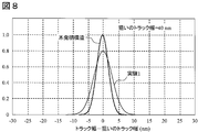
- FIG. 8 shows the result of a track width formation experiment using the differential read head of this example and the conventional structure.
- the vertical axis in the figure is the normalization frequency, and the horizontal axis is the difference between the actual track width and the target track width.
- the target track width was 40 nm.
- FIG. 8 confirms that the track width can be formed more accurately in the structure of this embodiment than in Experiment 1 for the differential read head having the conventional structure. Therefore, according to the present invention, the track width can be formed more accurately than the conventional structure by reducing the laminated film thickness.
- the substrate 15, the lower magnetic shield 30, the upper magnetic shield 31, and the insulating film 40 are not particularly limited in the present invention, and materials generally used are given as an example.
- the substrate 15 is AlTiC, SiC or those coated with Al 2 O 3
- the lower magnetic shield 30 and the upper magnetic shield 31 are Ni—Fe alloy and its nitride, Co—Zr, Co—Hf or Co
- a single layer or a multilayer film such as a Ta-based amorphous alloy may be used. These are easy to form by sputtering or plating.
- the first magnetoresistive film 200 / second magnetoresistive film 300 are preferably formed by sputtering from the viewpoint of controllability of film thickness and alloy composition and mass production efficiency.
- Film structure of the first magnetoresistance effect film 200 is, for example, Ta (5) from the substrate side in this order / Mn 80 Ir 20 (6) / Co 90 Fe 10 (2) / Ru (0.4) / Co 90 Fe 10 (3.5) / Ru (0.4) / Co 90 Fe 10 (2) / MgO (1) / Ni 85 Fe 15 (4) is a preferred example.
- the numerical value in () indicates the film thickness, and the unit is nm.
- the unit of each alloy composition indicated by the element suffix is at%.
- Mn 80 Ir 20 (6) is added to the first antiferromagnetic layer 236 by Co 90 Fe 10 (2) / Ru (0.4) / Co 90 Fe 10 (3.5) / Ru (0.4) / Co 90 Fe 10 (2) corresponds to the first fixed layer 230, MgO (1) corresponds to the first intermediate layer 220, and Ni 85 Fe 15 (4) corresponds to the first free layer 210.
- Ta (5) may be formed as a base layer of the first antiferromagnetic layer 236.
- Mg, Al, Si, Ti, V, Mn, Zr, Nb, Hf, Ta, and the like are included in addition to MgO.
- An oxide or nitride may be used as the intermediate layer material.
- the first intermediate layer is made of Cu, Ag, Au, or an alloy mainly composed of Cu, Ag, Au, it can be used as it is as a CPP-GMR film.
- the first intermediate layer may have a so-called “current confinement type” configuration in which a conductive path by a metallic pinhole such as Cu is formed in an insulating material such as Al 2 O 3 .
- the film structure of the second magnetoresistance effect film 300 for example, in order from the substrate side, Ta (3) Ru (4 ) / Mn 80 Ir 20 (6) / Co 90 Fe 10 (2) / Ru ( 0.4) / Co 90 Fe 10 (2) / MgO (1) / Ni 85 Fe 15 (4).
- the film thickness of the intermediate layer may be optimized as appropriate. The only difference is the configuration of the fixed layer.
- the second fixed layer 330 in the second magnetoresistive film 300 is / Co 90 Fe 10 (2) / Ru (0.4) / Co 90 Fe 10 (2).
- the first pinned layer 230 in the first magnetoresistive effect film 200 includes three Co—Fe layers
- the second pinned layer 330 in the second magnetoresistive effect film 300 includes two Co—Fe layers. There are differences in the inclusion.
- the first pinned layer 230 has a laminated ferrimagnetic structure in which m layers (m: odd number) of ferromagnetic layers and m ⁇ 1 antiferromagnetic interlayer coupling layers are alternately laminated
- the second pinned layer 330 has , A laminated ferrimagnetic structure in which n layers (n: even number) of ferromagnetic layers and n-1 layers of antiferromagnetic interlayer coupling layers are alternately laminated.
- the first magnetoresistive film 200 and the second magnetoresistive film 300 exhibit resistance change characteristics with opposite phases with respect to the signal magnetic field in the same direction, and are in a form suitable for differential operation. There is no problem even if it is replaced with m: even number and n: odd number.
- the film thickness of Ta (3) Ru (4) which is the underlayer of the antiferromagnetic material, may be changed.
- the magnetic read / write head of the first embodiment can realize a differential read head with high resolution and reduced spin torque noise by reducing the laminated film thickness. Furthermore, narrow track width can be easily formed by reducing the laminated film thickness.
- FIG. 9 shows a configuration example of the differential read head 20 ′ according to the second embodiment.
- the differential read head of Example 2 differs from Example 1 only in the stacking order of the free layer, the intermediate layer, and the fixed layer in the first magnetoresistive effect element and the second magnetoresistive effect element.
- the first magnetoresistive effect element 200 is laminated in order of the first free layer 210, the first intermediate layer 220, and the first fixed layer 230 from the substrate side
- the second magnetoresistive effect element 300 is stacked. Is a structure in which the second free layer 310, the second intermediate layer 320, and the first fixed layer 330 are laminated in this order from the substrate side.
- Example 1 the sum of the film thicknesses of the second fixed layer 330 and the second intermediate layer 320 is substantially G l , whereas in Example 2, the first intermediate layer 220 and the first intermediate layer 320 are The sum of the film thicknesses of the fixed layer 230 is substantially Gl . Therefore, also in the second embodiment, the laminated film thickness can be reduced as compared with the differential read head having the conventional structure, and high resolution can be realized. In addition, since the current is passed only in one direction from the free layer to the fixed layer or from the fixed layer to the free layer, spin torque noise can be reduced.
- the first magnetoresistive element 200 has Ni 85 Fe 15 (4) / MgO (1) / Co 90 Fe 10 (2) / Ru (0.4) in order from the substrate 15 side. ) / Co 90 Fe 10 (2) / Mn 80 Ir 20 (6) / Ta (3) Ru (4).
- Ni 85 Fe 15 (4) is the first free layer 210 and MgO (1) is the first intermediate layer 220, and Co 90 Fe 10 (2) / Ru (0.4) / Co 90 Fe 10.
- (2) / Mn 80 Ir 20 (6) corresponds to the first fixed layer 230.
- Mn 80 Ir 20 (6) / Co 90 Fe 10 (2) / Ru (0.4) / Co 90 Fe 10 (3.5) / Ru (0.4) / Co 90 Fe 10 (2) Is the second fixed layer 330
- MgO (1) is the second intermediate layer 320
- Ni 85 Fe 15 (4) is the second free layer 310.
- the differential read head of the present embodiment can realize high resolution by reducing the laminated film thickness, and can reduce spin torque noise peculiar to the CPP read head.
- FIG. 11 shows a differential read head according to the third embodiment of the present invention.
- the differential reproducing head 20 ′′ of Example 3 differs in the direction of energization to the laminated film compared to the head of Example 1.
- the lower electrode 50 in the configuration of FIG.
- the first electrode 52 and the second electrode 53 are provided independently at both ends in the track width direction of the first magnetoresistive element 200 and the second magnetoresistive element 300, respectively.
- the first permanent magnet film 451 is provided outside the first magnetoresistive effect film 200 in the track width direction
- the second permanent magnet film 453 is provided outside the second magnetoresistive effect film 300.
- it has an electric circuit for detecting the series sum or difference of the outputs of the two magnetoresistive elements 200 and 300.
- the film configurations of the first magnetoresistive element 200 and the second magnetoresistive element 300 are the same as those shown in FIG. 1 of Example 1 except that the first intermediate layer 220 and the second intermediate layer 320 are Cu. It is the same as the structure shown.
- This embodiment is a CIP-GMR film, and if the intermediate layer is an insulator, the magnetoresistive effect does not occur, and so-called tunnel magnetoresistive film cannot be used.
- materials for the first intermediate layer 220 and the second intermediate layer 320 materials such as Cu, Au, and Ag are generally used. There is no limit.
- the insulating layer 110 is inserted between the first magnetoresistive effect element 200 and the second magnetoresistive effect element 300 in order to allow current to flow independently through the two magnetoresistive effect elements 200 and 300.
- the insulating layer 110 must be an insulator or have a sufficiently large resistance compared to the magnetoresistive film. Since the material of the insulating layer 110 is not particularly limited, it can be a commonly used material such as Al 2 O 3 , SiO 2 , AlN, SiN, a mixture thereof, and a multilayer film. .
- the thickness of the insulating layer 110 is suitably 1 nm or more and 10 nm or less.
- the thickness of the insulating layer 110 is 1 nm or more, the upper and lower magnetoresistive elements can be sufficiently insulated. In addition, if the thickness of the insulating layer 110 is too large, the reproduction characteristics are deteriorated, so that it is preferably about 10 nm or less.
- This insulating layer 110, a second fixed layer 330 and the sum of the thickness of the second intermediate layer 320 of G 1 becomes, as described in Example 1, G l reproduction characteristics of differential read head This is because it is an important parameter that determines the above.
- the second is a system in which two magnetoresistive elements have an output having the same phase with respect to a medium magnetic field in the same direction, and a difference between outputs obtained from the two magnetoresistive elements is detected by an electric circuit.
- FIG. 13 shows a typical circuit diagram for electrically detecting a difference.
- a current can be independently passed through each magnetoresistive effect element, the output voltage can be detected independently, and differential detection can be performed by taking this difference.
- the outputs of the individual magnetoresistive elements may be in the same phase with respect to the same magnetic field.
- the number of ferromagnetic layers of the second pinned layer 330 can be made the same.
- the first method has the advantage that the electrical circuit is simpler than the second method.
- the second method has an advantage that the configuration of the fixed layer of the first magnetoresistance effect element 200 or the second magnetoresistance effect element 300 can be simplified.
- the laminated film thickness can be reduced in the CIP-GMR type differential read head, high resolution can be realized, and the track width can be formed more accurately than the conventional differential read head structure. It is possible.
- Example 3 the amount of current flowing through the two magnetoresistive elements can be controlled so as to compensate for the difference in the reproduction output of the individual magnetoresistive elements, so that it is easy to suppress the baseline shift.
- the first and second embodiments have an advantage that the MR ratio of each magnetoresistive element, that is, the reproduction output is large because of the structure in which a current can flow vertically in the film plane.
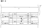
- FIG. 14 shows a configuration example of a differential read head according to the fourth embodiment of the present invention.
- the differential read head 20 ′ ′′ of the fourth embodiment is different from the third embodiment in the stacking order of the free layer, the intermediate layer, and the fixed layer in the first magnetoresistive element and the second magnetoresistive element.
- the first magnetoresistive element 200 is laminated in order of the first free layer 210, the first intermediate layer 220, and the first fixed layer 230 from the substrate side
- the second magnetoresistive element is In this structure, the second free layer 310, the second intermediate layer 320, and the second fixed layer 330 are stacked in this order from the substrate side.
- Example 3 the sum of the film thicknesses of the second fixed layer 330 and the second intermediate layer 320 is substantially G l , whereas in Example 4, the first intermediate layer 220 and The sum of the film thicknesses of the first fixed layer 230 is substantially Gl . Further, the permanent magnet film 451 and the permanent magnet film 452 are arranged at positions close to the first free layer 210 and the second free layer 310, respectively.
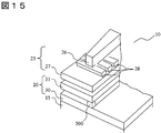
- FIG. 15 is a schematic perspective view showing a configuration example of a magnetic recording / reproducing head
- FIG. 16 is a schematic diagram of a magnetic recording / reproducing apparatus (magnetic disk apparatus) on which the magnetic recording / reproducing head 10 is mounted.
- the magnetic recording / reproducing head 10 includes a differential reproducing head (lower magnetic shield 30, laminated structure 500, upper magnetic shield 31) 20 and recording head (main magnetic pole 26, sub magnetic pole) on a substrate 15. 27, coil 28) 25.
- the perpendicular recording head (recording head) 25 may be provided with a shield, a light source for heating the perpendicular magnetic recording medium 500, and the like in order to assist magnetic recording.
- a trailing shield, a leading shield, and a side shield can be provided on the trailing side, leading side, and both sides in the track width direction of the main magnetic pole 26, respectively.
- a wraparound shield in which a trailing shield and a side shield are connected can also be provided.
- an optical probe having a light emitting element and a waveguide for heating the magnetic recording medium 500 may be provided at a position close to the main magnetic pole 26.
- the magnetic recording / reproducing apparatus 1000 rotates the disk 500 on which information is magnetically recorded by the spindle motor 600 and guides the head slider 700 onto the track of the disk 500 by the actuator 800.
- the head slider 700 is equipped with a magnetic recording / reproducing head provided with the differential reproducing head of the present invention, and moves relative to a predetermined recording position on the disk 500 to sequentially write and read signals.
- the actuator 800 can be a rotary actuator or a microactuator.
- the recording signal is recorded on the disk 500 by the recording head through the signal processing system 900, and the output of the differential reproducing head 20 is obtained as a reproduction signal through the signal processing system 900. Further, when the magnetic recording / reproducing head 10 is moved onto a desired recording track, the track position is detected using a highly sensitive output from the actuating reproducing head 20, and the actuator 800 is controlled to position the head slider 700. Do.
- the disk 500 may be a so-called continuous medium having a perpendicular magnetization film that is magnetized in a direction perpendicular to the film surface as a recording layer, and each bit is continuously present, or a non-writable medium that cannot be written by a recording head between a plurality of tracks.
- a so-called discrete track medium provided with a magnetic region may be used.
- a so-called patterned medium including a convex magnetic pattern and a nonmagnetic material filling a concave portion between the magnetic patterns on the substrate may be used.
- the disk 500 may have a perpendicular magnetization film on both sides to record information. When information is recorded on both sides of the disk, the head slider 700 is disposed on both sides of the disk.
Landscapes
- Engineering & Computer Science (AREA)
- Manufacturing & Machinery (AREA)
- Magnetic Heads (AREA)
- Hall/Mr Elements (AREA)
Abstract
高分解かつ高トラック幅形成精度が実現できる差動型再生ヘッドを提供する。 第1の磁気抵抗効果素子200は基板側から順に第1の固定層230、第1の中間層220、第1の自由層210の順に積層し、第2の磁気抵抗効果素子300は、その上に第2の固定層330、第2の中間層320、第2の自由層310の順に積層する。第2の固定層330及び第2の中間層320が実質的な差動ギャップの役割を担う。
Description
本発明は、差動型再生ヘッドと記録ヘッドを備える磁気記録再生ヘッド及びこの磁気記録再生ヘッドを搭載した磁気記録再生装置に関するものである。
近年、HDD(Hard Disk Drive)などの磁気記録再生装置においては、急速な記録密度の増加が求められており、磁気ヘッドや磁気メディア等も高記録密度を実現するものが求められている。磁気記録再生装置に再生素子として搭載する磁気抵抗効果ヘッドとしては、強磁性金属層を非磁性金属層を介して積層した多層膜の磁気抵抗効果を利用した、スピンバルブと呼ばれる構造が用いられている。磁気抵抗効果とは、中間層を挟んだ2層の強磁性層の磁化と磁化のなす角によって電気抵抗が変化する現象である。磁気抵抗効果を用いたスピンバルブは、反強磁性層/強磁性層/非磁性中間層/強磁性層の構造を有し、反強磁性層/強磁性層の界面に発生する交換結合磁界により反強磁性層と接した強磁性層の磁化を実質的に固定し、他方の強磁性層の磁化が外部磁界によって自由に回転することで出力を得る。上記反強磁性層と磁化が反強磁性層により実質的に固定される強磁性層は総称して固定層、上記磁化が外部磁場によって回転する強磁性層は自由層、上記非磁性中間層は中間層と呼ばれる。抵抗の変化率はMR(Magneto-Resistive)比と呼ばれ、MR比が高いほど再生出力を大きくできる。
磁気抵抗効果を利用したスピンバルブには、従来は、電流を積層膜の面内方向に流して用いるCIP(Current In the Plane)-GMR(Giant Magneto-Resistive)ヘッドが採用されてきた。現在では、積層膜の膜厚方向に電流を流して用いるTMR(Tunneling Magneto-Resistive)ヘッドや、CPP(Current Perpendicular to the Plane)-GMRヘッドへと移行しつつある。TMRヘッドやCPP-GMRヘッドはCIP-GMRヘッドと比較して、MR比を大きくできるためである。
現状の磁気抵抗効果ヘッドは、下部磁気シールドと上部磁気シールドで磁気抵抗効果膜を挟む構成(いわゆるシールド型再生ヘッド)となっていが、線記録密度方向の再生分解能は、この上下磁気シールドの間隔(Gs)に大きく依存する。ここで、線記録密度とは磁気記録媒体の円周方向のビット密度である。磁気記録媒体の半径方向のビット密度はトラック密度と呼び、両者を増大することで磁気記録再生装置の面記録密度が向上する。再生分解能とは、高記録密度記録時における再生出力が、低記録密度記録時と比較してどの程度の大きさを維持できるかを示す指標である。即ち、上下磁気シールド間隔を狭くするほど、線記録密度方向の分解能が高くなり、高い面記録密度を実現することができる。
しかし、現状製品に用いられている磁気抵抗効果ヘッドの構造では、磁気抵抗効果膜の膜厚は20~30nm程度以下にすることは不可能であり、再生分解能の向上には近い将来に限界が生じると考えられている。その理由は、上述した磁気抵抗効果膜(反強磁性層/強磁性層/非磁性中間層/強磁性層)の膜厚は、物理的に20~30nm程度が薄膜化の限界であることである。このため、現行構造の再生ヘッドでは上下磁気シールド間隔は20~30nm程度より狭くすることができず、高い面記録密度実現に向けた大きな障害となっている。
線記録密度方向の分解能を向上する手段として、いわゆる差動型再生ヘッドが提案されている。面内磁気記録方式では、磁気記録媒体に書かれた記録ビットに対して、磁化反転領域からのみ信号磁界が生じるのに対して、垂直磁気記録方式では、各記録ビットから必ず信号磁界が生じる。従って、垂直磁気記録方式は差動型再生ヘッドの使用に対して都合が良い。特許文献1には、垂直磁気記録方式を用いた磁気記録再生装置において、一対の磁気抵抗効果膜を導電材料からなる差動中間層を介して直列接続し、差動動作させる再生ヘッド構造が開示されている。一対の磁気抵抗効果膜のうち、信号磁界の感磁部となる2層の自由層が導電層を介して隣接対面するように配置され、一対の磁気抵抗効果膜の抵抗変化特性が、同じ向きの磁界に対して逆極性になるように設定することで、差動動作させることが可能となる。差動型再生ヘッドの線記録密度方向の分解能は、上下磁気シールド間隔よりも自由層間の内側の距離に大きく影響を受ける。したがって、差動型再生ヘッドでは一対の磁気抵抗効果膜間に介在する導電層の膜厚を薄膜化することで、現行型再生ヘッドよりも線密度方向の高い再生分解能が得られると考えられている。さらに、特許文献2には、2層の磁気抵抗効果素子が同じ向きの磁界に対して逆極性の抵抗変化特性が得られるさらに詳細な差動型再生ヘッドの構造が開示されている。
差動型再生ヘッドは2つの磁気抵抗効果素子とその間に差動中間層を積層した構造を有し、2つの磁気抵抗効果素子の自由層、中間層、固定層は差動中間層を介して鏡面対称に配置されている。このため、積層膜厚は現行の再生ヘッドの2.5倍から3倍程度にまで厚くなってしまう。積層膜厚が増大すると、主に、(1)再生特性の悪化、(2)ウエハプロセスの高難度化の問題が生じる。
再生特性の悪化は具体的には、厚膜化により分解能が低下してしまうことである。差動型再生ヘッドの分解能は、個々の磁気抵抗効果素子の磁気シールド間隔と差動中間層の大きさに依存するが、積層膜厚の厚膜化により上下の磁気シールド間隔が広がると、個々の磁気抵抗効果素子の再生遷移幅が大きくなるため、分解能が低下する。分解能は差動中間層の膜厚を薄膜化すると向上するが、これに伴い孤立波出力が減少するため、差動中間層の薄膜化にも限界がある。したがって、差動型再生ヘッドにおいても、分解能を向上させるためには積層膜厚の薄膜化が必要である。
ウエハプロセスの高難度化は具体的には、狭トラック幅形成が困難になることである。一般的に、トラック幅形成は層膜厚に対しトラック幅が広い方が容易である。現状はトラック幅80nmに対し積層膜厚が35nm程度であるので、トラック幅形成は比較的容易である。しかし、差動型再生ヘッドでは積層膜厚が70nm程度であるので、積層膜厚の方がトラック幅よりも大きくトラック幅形成が困難になる。したがって、ウエハプロセスの観点からも差動ヘッドの膜厚は薄いほうが好ましい。
ウエハプロセスの高難度化は、また、積層膜厚の増加に伴う素子パターン形成プロセスが困難になることを指す。積層膜厚が増加すると、トラック幅及び素子高さのパターン形成時に積層膜を除去するイオンミリングやドライエッチングの除去量が増大し、マスクの耐性不足やイオンミリングの再付着量増大が発生しやすくなる。このことがパターンの変形や、側壁の導電性再付着物起因のシャント電流による不良に結びつく。またイオンミリングやドライエッチング後のマスク残膜厚の減少は、リフトオフプロセスの歩留まり低下を引き起こす原因となるため好ましくない。加えて、差動型再生ヘッドを適用する世代ではトラック幅のターゲットが50nm以下と現行より縮小することから、より微細化加工が可能な薄膜のレジストマスクが必要となり、厚い積層膜の差動型再生ヘッドのプロセスがより困難になると予想できる。
差動型再生ヘッドには、膜厚の増加に伴う以上のような問題が存在し、膜厚の低減が重要な課題である。しかし、従来の差動型ヘッドは2つの磁気抵抗効果素子とその中間に差動中間層を設ける構成であり、差動中間層の薄膜化は大幅な再生特性の劣化を招くため、各磁気抵抗効果素子の膜厚を低減する以外には、積層膜厚を低減する方法はないのが現状である。ところが、前述したように個々の磁気抵抗効果素子の薄膜化は25~30nm程度が限界であるため、差動型再生ヘッドの積層膜厚を70nm程度以下に薄膜化する有効な方法は存在しない。これは、CIP-GMR、CPP型のTMRやCPP-GMRヘッドに共通の課題である。
一方、CPP型の差動型再生ヘッドには、スピントルクノイズが現行型再生ヘッドよりも発生しやすいという特有の問題がある。スピントルクノイズは電流方向に敏感であるため、現行の再生ヘッドではスピントルクノイズが小さい方向に電流を流すことでスピントルクノイズを低減できる。具体的には、固定層と自由層の磁化が反平行方向のときは電流を固定層から自由層へ通電し、固定層と自由層の磁化が平行方向のときは自由層から固定層へ通電することにより、スピントルクノイズを低減できる。しかし、差動型再生ヘッドの場合には、必ず電流が、固定層、中間層、自由層という経路と自由層、中間層、固定層という経路を通るため、どの方向に電流を流しても、どちらかの磁気抵抗効果素子で大きなスピントルクノイズが発生しやすいという問題が生じる。したがって、CPP型の差動型再生ヘッドではスピントルクノイズが現行の再生ヘッドよりも発生しやすく、その抑制がCPP型差動型再生ヘッドの課題である。
本発明の目的は、CPP型及びCIP型差動型再生ヘッドの積層膜厚を低減することにより、高分解能かつ狭トラック幅形成が可能な差動型再生ヘッドを実現することである。さらに、CPP型においては、ヘッドノイズの原因であるスピントルクノイズを低減することである。
本発明では、上記課題を解決する為に、垂直磁気記録方式を前提として、磁気記録再生ヘッドに、第1の自由層を有する第1の磁気抵抗効果素子と、第2の自由層を有する第2の磁気抵抗効果素子が積層された積層構造を有する差動動作型の再生ヘッドを設ける。第1の磁気抵抗効果素子と第2の磁気抵抗効果素子には、反強磁性層/固定層/非磁性中間層/自由層の積層構造を有するスピンバルブ型磁気抵抗効果素子を用いる。ここで反強磁性層は固定層の磁化を実質的に固定するための交換結合バイアスを印加するものであって、直接固定層に密着して形成しても、間接的に磁気的結合を経て効果をもたらしてもよい。あるいは反強磁性層の替わりに他のバイアス印加手段、例えば、硬磁性膜の残留磁化を用いたり、電流バイアスを用いたりしてもよい。
自由層は、膜厚と飽和磁化の積が異なる2つ以上の複数の自由層を反平行結合層を介してお互いの磁化が反平行になるように結合した、積層フェリ自由層を用いても良い。固定層は、第1の固定層と第2の固定層が反平行結合層を介してお互いの磁化が反平行になるように結合した、積層フェリ固定層を用いてもよい。このとき、その結合は感知すべき磁場に対して十分に大きいことが必要である。具体的な反平行結合磁界の大きさは数百から数千エルステッド程度である。その結果、第2の固定層の磁化は感知すべき磁場に対して固定している。自由層は感知すべき磁場に対応して磁化の方向を変化させる。感知すべき磁場に対応して方向を変化させる自由層の磁化と、感知すべき磁場に対して固定している固定層あるいは積層フェリ固定層の第2の固定層の磁化の相対角度により出力が発生する。
自由層を単磁区化するために、バイアス層を配置する。このバイアス層は、望ましくは感知すべき磁界に対して十分大きな保磁力を有する高保磁力膜を、自由層のトラック幅方向の端部に互いの端部が近接するように配置したものである。
このような磁気記録再生ヘッドにおいて、膜厚の低減を目的として、本発明では、さらに第1の磁気抵抗効果素子の固定層もしくは第2の磁気抵抗効果素子の第2の固定層のどちらか一方が、実質的に差動ギャップの役割もしくはその役割の一部を担う構成とする。より具体的には、
(1)第1の磁気抵抗効果素子は基板側から第1の自由層、第1の中間層、第1の固定層が順次積層された構造であり、第2の磁気抵抗効果素子は基板側から第2の自由層、第2の中間層、第2の固定層が順次積層された構造。
(1)第1の磁気抵抗効果素子は基板側から第1の自由層、第1の中間層、第1の固定層が順次積層された構造であり、第2の磁気抵抗効果素子は基板側から第2の自由層、第2の中間層、第2の固定層が順次積層された構造。
(2)第1の磁気抵抗効果素子は基板側から第1の固定層、第1の中間層、第1の自由層が順次積層された構造であり、第2の磁気抵抗効果素子は基板側から第2の固定層、第2の中間層、第2の自由層が順次積層された構造。
(3)上記(1)、(2)の構成において、積層膜の上下方向の外側に膜面垂直方向に電流を通電するための電極を有するCPP型素子もしくは、積層膜の膜面内方向に電流を通電するための電極をトラック幅方向の外側に有するCIP型素子であること。
このように固定層が実質的な差動中間層の役割を兼ねる構成とすることで、差動型再生ヘッドの総膜厚を低減することが可能となり、磁気シールド間隔の狭小化による分解能の増加と再生出力の増加、狭トラック幅形成プロセスの簡易化が可能となる。更に、CPP型のヘッドにおいてはスピントルクノイズも低減する。
本発明によれば、積層膜厚の低下による再生特性の向上と狭トラック形成プロセスの簡易化が可能となる。
以下、図面を参照して本発明の実施の形態を説明する。理解を容易にするため、以下の図において同じ機能部分には同一の符号を付して説明する。
[実施例1]
図1に、本発明の実施例1による差動型再生ヘッドのABS(Air bearing surface)面から見た概略図を示す。なお、図中には各強磁性層の磁化方向を矢印で付記してある。参考のために、図2に従来の差動型再生ヘッドの積層構造を示す。本実施例の差動型再生ヘッド10は、基板15側から、第1の磁気抵抗効果素子200と第2の磁気抵抗効果素子300を順に積層した積層構造400を有する。第1と第2の磁気抵抗効果素子は、磁場に対し逆位相の抵抗変化が得られるように設定する。再生ヘッド10の第1の磁気抵抗効果素子200は第1の自由層210を、第2の磁気抵抗効果素子300は第2の自由層310を有し、第1の自由層210と第2の自由層310の間の距離をGlと定義する。
図1に、本発明の実施例1による差動型再生ヘッドのABS(Air bearing surface)面から見た概略図を示す。なお、図中には各強磁性層の磁化方向を矢印で付記してある。参考のために、図2に従来の差動型再生ヘッドの積層構造を示す。本実施例の差動型再生ヘッド10は、基板15側から、第1の磁気抵抗効果素子200と第2の磁気抵抗効果素子300を順に積層した積層構造400を有する。第1と第2の磁気抵抗効果素子は、磁場に対し逆位相の抵抗変化が得られるように設定する。再生ヘッド10の第1の磁気抵抗効果素子200は第1の自由層210を、第2の磁気抵抗効果素子300は第2の自由層310を有し、第1の自由層210と第2の自由層310の間の距離をGlと定義する。
図2に示す従来構造の差動型再生ヘッドでは、Glは実質的に2つの磁気抵抗効果素子の中間に設けられた差動中間層100の膜厚となる。したがって、従来構造の差動型再生ヘッドの積層膜厚は、差動中間層100の膜厚と第1の磁気抵抗効果素子200の膜厚と第2の磁気抵抗効果素子300の膜厚の和となる。一方、本実施例では、Glは第2の固定層330と第2の中間層320の膜厚の和となる。本発明では固定層と中間層が実質的な差動ギャップの役割を担うため、特に2つの磁気抵抗効果素子の中間に差動中間層100を挿入する必要は生じず、積層膜厚を従来構造よりも薄くすることができる。
また、第1の磁気抵抗効果素子200と第2の磁気抵抗効果素子300のトラック幅方向の両側には、自由層を単磁区化するための永久磁石膜450を設けることができる。2つの磁気抵抗効果素子の外側(上下)には、電流を膜厚の垂直方向に流すための一対の電極を設ける。電極は、基板15に近い方を下部電極50、基板15から遠い方を上部電極51と呼ぶ。下部及び上部電極の代わりに、導電性の強磁性体を用いて電極と磁気シールドの役割を兼ねるようにしても良い。
Glは差動型ヘッドの再生出力と分解能を決定する重要なパラメータの一つであるため、適切に設定することが必要である。ここで、再生出力Slfは低記録密度における出力と定義し、分解能は磁気記録再生装置で使用する線記録密度の1/2の線記録密度における出力SmfとSlfの比Smf/Slfと定義する。Glが小さいと分解能は高くなるが、小さすぎると再生出力が急激に低下するため、Glは適切に設定する必要がある。Glの設計値は、例えば線記録密度が1500kfciの磁気記録再生装置であれば、12nm以上20nm以下程度が適切である。
図3に、ABS面から見た差動型再生ヘッド20の詳細な構成例を示す。比較のため、図4に代表的な従来構造の再生ヘッドをABS面から見た詳細な構成例を示す。第1の磁気抵抗効果膜200の基本構成は、基板15側から順に、第1の固定層230/第1の中間層220/第1の自由層210である。勿論、最下層に適切な下地層を形成しても差し支えない。同様に、第2の磁気抵抗効果膜300の基本構成は、基板15に近い側から順に、第2の固定層330/第2の中間層320/第2の自由層310である。最上層に適切な保護層を形成しても差し支えない。
以下に、第1の磁気抵抗効果素子200と第2の磁気抵抗効果素子300が同一外部磁界方向に対して、逆位相の抵抗変化を示すための、第1の固定層230と第2の固定層330の構成例を示す。第1の固定層230は、第1の反強磁性層236と、m層(m:奇数)の強磁性層とm-1層の反強磁性的層間結合層を交互に積層したいわゆる積層フェリ構造の積層膜である。第2の固定層330は、n層(n:偶数)の強磁性層とn-1層の反強磁性的層間結合層を交互に積層した積層フェリ構造と、第2の反強磁性層334の積層膜である。こうすることによって、第1の反強磁性層236及び第2の反強磁性層334に接している強磁性層235,333(第1の固定層230及び第2の固定層330の構成要素)の磁化を同一方向に固定した場合、実質的に磁気抵抗効果に寄与する、第1の中間層220及び第2の中間層320に接する強磁性層231,331(第1の固定層230及び第2の固定層330の構成要素)の磁化は反平行な方向に固定される。従って、第1の磁気抵抗効果膜200と第2の磁気抵抗効果膜300は同一方向の信号磁界に対して、逆位相の抵抗変化特性を示す。なお、nが奇数で、mが偶数であってもよい。
高い分解能と再生出力を実現するために、さらに、差動型再生ヘッド20の積層構造400外側に、一対の電極50,51を介して一対の磁気シールドを設ける。基板15に近い方の磁気シールドが下部磁気シールド30、遠い方の磁気シールドが上部磁気シールド31である。磁気シールドを設けることにより、分解能をさらに向上させることが可能となる。
以下に、本発明により得られる再生特性の向上効果について説明する。なお、磁気記録再生装置の最高線記録密度は1500kfciであるとし、本実施例のGlは21nmであるとした。図5に、本実施例及び従来構造におけるヘッドSNRと積層膜厚を示す。ヘッドSNRは750kfciの出力であるSlfとヘッドノイズNhの比から求めたものである。図5よりわかるように、本実施例では従来構造よりもヘッドSNRを約2~4dB高くすることが可能である。
表1に本実施例の再生ヘッドと従来構造の再生ヘッドにおけるヘッドSNRの出力とヘッドノイズの内訳を示し、これを例にして本発明の効果を詳しく説明する。本実施例の差動型再生ヘッドの積層膜厚は50nmであり、従来構造の積層膜厚は70nmである。本実施例の第1の自由層210の膜厚は4nm、第1の中間層220の膜厚は1nm、第1の固定層230の膜厚は20nmであり、第2の自由層310の膜厚は4nm、第2の中間層320の膜厚は1nm、第2の固定層330の膜厚は20nmである。一方、従来構造も同様に、第1の自由層210の膜厚は4nm、第1の中間層220の膜厚は1nm、第1の固定層230の膜厚は20nmであり、第2の自由層310の膜厚は4nm、第2の中間層320の膜厚は1nm、第2の固定層330の膜厚は20nmであり、差動中間層100の膜厚は20nmである。

図6に、差動型再生ヘッドにおける分解能と磁気シールド間隔の関係を示す。差動型再生ヘッドにおいても、分解能は磁気シールド間隔の狭小化により向上することが分かる。しかし、図5に示すように、従来構造の差動型再生ヘッドでは積層膜厚を60~70nm程度以下にすることは、再生特性の大幅な劣化を招くため、現実的には不可能であった。これは前述したように、個々の磁気抵抗効果素子の膜厚は25nm程度が物理的に限界であり、積層膜厚を低減するにはGlを薄膜化する他に方法がないためである。しかし、Glを薄膜化しすぎると分解能の向上分以上に孤立波出力が低下するため、結果としてヘッドSNRの低下を招く。一方、本実施例では固定層330を実質的なGlとすることができるため、差動中間層分の膜厚である20nmを低減することができる。
次に、本実施例のもう一つの特色であるスピントルクノイズ低減効果について説明する。図7に、本実施例及び従来構造におけるヘッドノイズとセンス電流の関係を示す。センス電流方向は正が固定層から自由層方向、負が自由層から固定層方向と定義する。従来構造及び本実施例ともに、センス電流の増加に伴いヘッドノイズが増加する。これはスピントルクノイズとマグノイズの増加によるものである。本実施例では、電流が負のときには従来例よりもヘッドノイズが大きいが、電流が正の時には従来例よりも小さく、電流方向に対してヘッドノイズの大きさが非対称になることが特徴である。したがって、本実施例では電流を正に流すように設定する。本実施例では、電流方向が正のときにノイズが小さいが、負の時に小さいときには、電流を自由層から固定層方向へ流す。
本実施例においてヘッドノイズが電流方向に対して非対称になる理由は、電流が固定層から自由層もしくは自由層から固定層のどちらかにしか流れないことに起因している。スピントルクノイズは電流方向と自由層と固定層の磁化の相対角度に大きく依存する。差動型再生ヘッドでは第1の磁気抵抗効果素子と第2の磁気抵抗効果素子の特性は等しくなるように設計するので、各自由層と固定層の磁化の相対角度もほとんど等しくなる。したがって、本実施例におけるスピントルクノイズは電流方向のみに大きく依存することになり、電流方向に対してヘッドノイズの大きさが非対称となる。一方、従来例では電流は必ず固定層から自由層と自由層から固定層へと流れるため、ヘッドノイズは電流方向に依存しなくなる。
以上の理由により、本実施例では電流が自由層から固定層か、固定層から自由層かのどちらか一方向にしか流れないために、スピントルクノイズが小さくなる電流方向を選択することが可能となり、結果として従来構造よりもスピントルクノイズが低下する。
次に、本発明の特色の一つである積層膜厚の低減によるトラック幅精度の向上効果について説明する。図8に、本実施例及び従来構造の差動型再生ヘッドを用いたトラック幅形成実験の結果を示す。図の縦軸は規格化頻度であり、横軸は実測のトラック幅と狙いのトラック幅の差分である。本実験では狙いのトラック幅は40nmとした。図8より、本実施例の構造の方が従来構造の差動型再生ヘッドに対する実験1よりも精度良くトラック幅を形成できていることが確かめられる。したがって、本発明は積層膜厚を低減することにより、従来構造よりもトラック幅を精度良く形成することが可能である。
次に、図1及び図3に示した差動型再生ヘッド20を構成する各膜の具体的な組成及び膜厚について説明する。基板15、下部磁気シールド30及び上部磁気シールド31、絶縁膜40については、本発明において特別な限定を要するものではないため、一般的に用いられている材料を一例として挙げておく。基板15としては、AlTiC,SiC又はそれらにAl2O3を被覆したもの、下部磁気シールド30及び上部磁気シールド31としては、Ni-Fe合金及びその窒化物、Co-Zr又はCo-Hf又はCo-Ta系非晶質合金等の単層又は多層膜を用いればよい。これらは、スパッタ法やめっき法で形成するのが簡便である。絶縁膜40としては、Al2O3,SiO2,AlN,SiNやこれらの混合物及び多層膜を用いることで、下部磁気シールド30と上部磁気シールド31の短絡を防止することができる。これらは、スパッタ法で形成するのが簡便で好ましい。
第1の磁気抵抗効果膜200/第2の磁気抵抗効果膜300の形成は、膜厚及び合金組成の制御性や量産効率の観点から、スパッタ法により作製するのが好ましい。第1の磁気抵抗効果膜200の膜構成は、例えば、基板側から順にTa(5)/Mn80Ir20(6)/Co90Fe10(2)/Ru(0.4)/Co90Fe10(3.5)/Ru(0.4)/Co90Fe10(2)/MgO(1)/Ni85Fe15(4)などが好ましい一例である。( )内の数値は膜厚を示し、単位はnmである。また、元素の添え字で示した各合金組成の単位は、at%である。Mn80Ir20(6)が第1の反強磁性層236に、Co90Fe10(2)/Ru(0.4)/Co90Fe10(3.5)/Ru(0.4)/Co90Fe10(2)が第1の固定層230に、MgO(1)が第1の中間層220に、Ni85Fe15(4)が第1の自由層210にそれぞれ相当する。なお、Ta(5)を、第1の反強磁性層236の下地層として形成しても良い。また、ここでは第1の中間層としてMgOを用いたTMR膜の例を示したが、MgO以外にも、Mg,Al,Si,Ti,V,Mn,Zr,Nb,Hf,Taなどを含む酸化物あるいは窒化物を中間層材料として用いても差し支えない。また、第1の中間層にCu,Ag,Auやそれを主成分とした合金を用いる構成とすると、そのままCPP-GMR膜として使用し得る。更には、第1の中間層をAl2O3のような絶縁性材料の中にCuなどの金属的ピンホールによる伝導パスを形成した、いわゆる「電流狭窄型」の構成としても良い。
同様に、第2の磁気抵抗効果膜300の膜構成は、例えば、基板側から順に、Ta(3)Ru(4)/Mn80Ir20(6)/Co90Fe10(2)/Ru(0.4)/Co90Fe10(2)/MgO(1)/Ni85Fe15(4)のようにすると良い。面積抵抗や磁気抵抗変化率を微調整するためには、主に中間層の膜厚を適宜最適化すれば良い。唯一異なるのが、固定層の構成である。第2の磁気抵抗効果膜300中の第2の固定層330は、/Co90Fe10(2)/Ru(0.4)/Co90Fe10(2)としてある。どちらも、Co-Fe強磁性層と反強磁性的な層間結合をもたらすRu層を交互に積層した、いわゆる「積層フェリ」構成となっている。第1の磁気抵抗効果膜200中の第1の固定層230は3層のCo-Fe層、第2の磁気抵抗効果膜300中の第2の固定層330は2層のCo-Fe層を含んでいる点に相違がある。即ち、第1の固定層230は、m層(m:奇数)の強磁性層とm-1層の反強磁性的層間結合層を交互に積層した積層フェリ構造、第2の固定層330は、n層(n:偶数)の強磁性層とn-1層の反強磁性的層間結合層を交互に積層した積層フェリ構造としてある。
こうすることによって、第1の反強磁性層236に接している強磁性層235及び第2の反強磁性層334に接している強磁性層333の磁化を同一方向に固定した場合、実質的に磁気抵抗効果に寄与する第1の中間層220に接する強磁性層231及び第2の中間層320に接する強磁性層331の磁化は反平行な方向に固定される。従って、第1の磁気抵抗効果膜200と第2の磁気抵抗効果膜300が同一方向の信号磁界に対して、逆位相の抵抗変化特性を示し、差動動作に適した形態となる。なお、m:偶数、n:奇数と置き換えても何ら差し支えはない。Glの大きさを調整したい場合は、反強磁性体の下地層であるTa(3)Ru(4)の膜厚を変化させればよい。
以上説明したように、実施例1の磁気記録再生ヘッドは、積層膜厚を低減することにより、高い分解能とスピントルクノイズを低減した差動型再生ヘッドを実現できる。さらに、積層膜厚が低減することにより狭トラック幅形成も容易になる。
[実施例2]
実施例2による差動型再生ヘッド20′の構成例を図9に示す。実施例2の差動型再生ヘッドは、実施例1と比べて、第1の磁気抵抗効果素子及び第2の磁気抵抗効果素子における自由層、中間層と固定層の積層順序のみが異なる。具体的には、第1の磁気抵抗効果素子200は基板側から第1の自由層210、第1の中間層220、第1の固定層230の順に積層し、第2の磁気抵抗効果素子300は基板側から第2の自由層310、第2の中間層320、第1の固定層330の順に積層した構造である。実施例1では第2の固定層330と第2の中間層320の膜厚の和が実質的なGlとなるのに対して、実施例2では、第1の中間層220と第1の固定層230の膜厚の和が実質的なGlとなる。したがって、実施例2においても、従来構造の差動型再生ヘッドよりも積層膜厚を低減することが可能であり、高分解能を実現できる。また、電流も自由層から固定層の方向もしくは、固定層から自由層の方向の一方向にしか通電しないため、スピントルクノイズを低減することができる。
実施例2による差動型再生ヘッド20′の構成例を図9に示す。実施例2の差動型再生ヘッドは、実施例1と比べて、第1の磁気抵抗効果素子及び第2の磁気抵抗効果素子における自由層、中間層と固定層の積層順序のみが異なる。具体的には、第1の磁気抵抗効果素子200は基板側から第1の自由層210、第1の中間層220、第1の固定層230の順に積層し、第2の磁気抵抗効果素子300は基板側から第2の自由層310、第2の中間層320、第1の固定層330の順に積層した構造である。実施例1では第2の固定層330と第2の中間層320の膜厚の和が実質的なGlとなるのに対して、実施例2では、第1の中間層220と第1の固定層230の膜厚の和が実質的なGlとなる。したがって、実施例2においても、従来構造の差動型再生ヘッドよりも積層膜厚を低減することが可能であり、高分解能を実現できる。また、電流も自由層から固定層の方向もしくは、固定層から自由層の方向の一方向にしか通電しないため、スピントルクノイズを低減することができる。
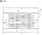
実施例2の積層膜の詳細例を図10に示す。本例は実施例1の構成とは積層膜の順序のみが異なっているので、積層順以外についての詳細な説明は省略する。本例における積層膜の構成は、第1の磁気抵抗効果素子200は基板15側から順に、Ni85Fe15(4)/MgO(1)/Co90Fe10(2)/Ru(0.4)/Co90Fe10(2)/Mn80Ir20(6)/Ta(3)Ru(4)のようにすると良い。ここでNi85Fe15(4)は第1の自由層210、MgO(1)は第1の中間層220であり、Co90Fe10(2)/Ru(0.4)/Co90Fe10(2)/Mn80Ir20(6)は第1の固定層230に相当する。一方、第2の磁気抵抗効果素子300は例えば、基板側から順に、Ni85Fe15(4)/MgO(1)/Co90Fe10(2)/Ru(0.4)/Co90Fe10(3.5)/Ru(0.4)/Co90Fe10(2)/Mn80Ir20(6)/Ta(5)のようにすると良い。ここで、Mn80Ir20(6)/Co90Fe10(2)/Ru(0.4)/Co90Fe10(3.5)/Ru(0.4)/Co90Fe10(2)は第2の固定層330、MgO(1)は第2の中間層320であり、Ni85Fe15(4)は第2の自由層310である。
本実施例の差動型再生ヘッドは実施例1の構成と同様に、積層膜厚を低減することにより高分解能を実現でき、またCPP型再生ヘッド特有のスピントルクノイズを低減することができる。
[実施例3]
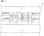
本発明の実施例3の差動型再生ヘッドを図11に示す。実施例3の差動型再生ヘッド20”は、実施例1のヘッドと比較して、積層膜への通電方向が異なる。実施例3では、実施例1の図1の構成における下部電極50と上部電極51が無く、その代わりに第1の磁気抵抗効果素子200と第2の磁気抵抗効果素子300のトラック幅方向の両端に、それぞれ第1の電極52と第2の電極53を独立に設けている。これに伴い、第1の磁気抵抗効果膜200のトラック幅方向の外側に第1の永久磁石膜451を設け、第2の磁気抵抗効果膜300の外側に第2の永久磁石膜453を設けている。さらに、2つの磁気抵抗効果素子200,300の出力の直列和、あるいは差分を検出するための電気回路を有する。
本発明の実施例3の差動型再生ヘッドを図11に示す。実施例3の差動型再生ヘッド20”は、実施例1のヘッドと比較して、積層膜への通電方向が異なる。実施例3では、実施例1の図1の構成における下部電極50と上部電極51が無く、その代わりに第1の磁気抵抗効果素子200と第2の磁気抵抗効果素子300のトラック幅方向の両端に、それぞれ第1の電極52と第2の電極53を独立に設けている。これに伴い、第1の磁気抵抗効果膜200のトラック幅方向の外側に第1の永久磁石膜451を設け、第2の磁気抵抗効果膜300の外側に第2の永久磁石膜453を設けている。さらに、2つの磁気抵抗効果素子200,300の出力の直列和、あるいは差分を検出するための電気回路を有する。
第1の磁気抵抗効果素子200と第2の磁気抵抗効果素子300の膜構成は、第1の中間層220及び第2の中間層320がCuであることを除いて実施例1の図1に示した構成と同一である。本実施例はCIP-GMR膜であり、中間層が絶縁体であると磁気抵抗効果を生じないため、所謂トンネル磁気抵抗効果膜を用いることはできない。第1の中間層220及び第2の中間層320の材料としては、Cu,Au,Agなどの材料が用いられるのが一般的であるが、磁気抵抗効果を生じる材料であること以外には特に制限はない。本実施例では、2つの磁気抵抗効果素子200,300に独立に電流を流すために、絶縁層110を第1の磁気抵抗効果素子200と第2の磁気抵抗効果素子300の間に挿入する。絶縁層110は絶縁体であるか、もしくは抵抗が磁気抵抗効果膜と比較して十分に大きい必要がある。絶縁層110の材料は、特別な限定を要するものではないため、一般的に用いられている材料、例えばAl2O3,SiO2,AlN,SiNやこれらの混合物及び多層膜とすることができる。絶縁層110の膜厚は1nm以上、10nm以下が適当である。絶縁層110の膜厚は1nm以上であれば、十分に上下の磁気抵抗効果素子を絶縁することができる。また、絶縁層110の膜厚が厚すぎると再生特性の低下を招くため、10nm程度以下が好ましい。これは、絶縁層110、第2の固定層330と第2の中間層320の膜厚の和はG1となり、実施例1で説明したように、Glは差動型再生ヘッドの再生特性を決める重要なパラメータであるためである。
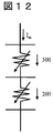
2つの磁気抵抗効果素子の差動出力を得るためには、2つの方法がある。一つは2つの磁気抵抗効果素子が同一方向の媒体磁界に対して逆位相の出力を有する構成とし、図12に模式的に示すように、各磁気抵抗効果素子の出力を電気回路を用いて直列に加算する方式である。このような構成を用いることにより、実施例1、2の構成と同様に、差動出力を生じることができる。
2つ目は、2つの磁気抵抗効果素子は同一方向の媒体磁界に対して同一位相の出力を有する構成とし、2つの磁気抵抗効果素子から得られる出力の差分を電気回路により検出する方式である。図13に電気的に差分を検出するための代表的な回路図を示す。この回路では、個々の磁気抵抗効果素子に独立に電流を流し、出力電圧を独立に検出して、この差分をとることにより差動検出ができる。また、この構成の場合には、一つ目の構成や実施例1、2とは異なり、個々の磁気抵抗効果素子の出力は同一磁界に対して同位相でよいため、第1の固定層230及び第2の固定層330の強磁性層の積層回数を同一にすることができる。
1つ目の方式は、電気回路が2つ目の方式よりも単純であるという利点がある。一方、2つ目の方式は、第1の磁気抵抗効果素子200あるいは第2の磁気抵抗効果素子300の固定層の構成を単純にできるという利点がある。
本構成例はCIP-GMR型の差動型再生ヘッドにおいて積層膜厚を低減することができるため、高い分解能を実現でき、かつ従来の差動型再生ヘッド構造よりもトラック幅を精度良く形成することが可能である。
さらに、実施例3には、個々の磁気抵抗効果素子の再生出力の差分を補償するように、2つの磁気抵抗効果素子に流す電流量を制御することができるため、ベースラインシフトを抑制しやすいという利点がある。一方、実施例1、2には、膜面内に垂直に電流を流せる構造のために、個々の磁気抵抗効果素子のMR比すなわち再生出力が大きいという利点がある。
[実施例4]
本発明の実施例4による差動型再生ヘッドの構成例を図14に示す。実施例4の差動型再生ヘッド20'''は、実施例3と比較して、第1の磁気抵抗効果素子及び第2の磁気抵抗効果素子における自由層、中間層と固定層の積層順序が異なる構成である。具体的には、第1の磁気抵抗効果素子200は基板側から第1の自由層210、第1の中間層220、第1の固定層230の順に積層し、第2の磁気抵抗効果素子は基板側から第2の自由層310、第2の中間層320、第2の固定層330の順に積層した構造である。実施例3の構成では第2の固定層330と第2の中間層320の膜厚の和が実質的なGlとなるのに対して、実施例4においては、第1の中間層220と第1の固定層230の膜厚の和が実質的なGlとなる。また、永久磁石膜451及び永久磁石膜452は、それぞれ第1の自由層210及び第2の自由層310に近接する位置に配置する。
本発明の実施例4による差動型再生ヘッドの構成例を図14に示す。実施例4の差動型再生ヘッド20'''は、実施例3と比較して、第1の磁気抵抗効果素子及び第2の磁気抵抗効果素子における自由層、中間層と固定層の積層順序が異なる構成である。具体的には、第1の磁気抵抗効果素子200は基板側から第1の自由層210、第1の中間層220、第1の固定層230の順に積層し、第2の磁気抵抗効果素子は基板側から第2の自由層310、第2の中間層320、第2の固定層330の順に積層した構造である。実施例3の構成では第2の固定層330と第2の中間層320の膜厚の和が実質的なGlとなるのに対して、実施例4においては、第1の中間層220と第1の固定層230の膜厚の和が実質的なGlとなる。また、永久磁石膜451及び永久磁石膜452は、それぞれ第1の自由層210及び第2の自由層310に近接する位置に配置する。
本構成例においても従来構造の差動型再生ヘッドよりも積層膜厚を低減することが可能であり、高い分解能を実現でき、かつ従来の差動型再生ヘッド構造よりもトラック幅を精度良く形成することが可能である。
[実施例5]
図15は、磁気記録再生ヘッドの構成例を示す斜視模式図であり、図16は、その磁気記録再生ヘッド10を搭載した磁気記録再生装置(磁気ディスク装置)の概略図である。
図15は、磁気記録再生ヘッドの構成例を示す斜視模式図であり、図16は、その磁気記録再生ヘッド10を搭載した磁気記録再生装置(磁気ディスク装置)の概略図である。
図15に示すように、磁気記録再生ヘッド10は、基板15上に差動型再生ヘッド(下部磁気シールド30、積層構造500、上部磁気シールド31)20と、記録ヘッド(主磁極26、副磁極27、コイル28)25を有する。垂直記録ヘッド(記録ヘッド)25には、磁気記録を補助するために、シールドや垂直磁気記録媒体500を熱するための光源等が備えられていてもよい。たとえば、主磁極26のトレーリング側、リーディング側、トラック幅方向の両側には、それぞれトレーリングシールド、リーディングシールド、サイドシールドを設けることができる。また、トレーリングシールドとサイドシールドが連結したラップアラウンドシールドを設けることもできる。また、主磁極26に近接する位置に、磁気記録媒体500を熱するための、発光素子と導波路を有する光プローブを設けてもよい。
磁気記録再生装置1000は、磁気的に情報を記録するディスク500をスピンドルモータ600にて回転させ、アクチュエータ800によってヘッドスライダ700をディスク500のトラック上に誘導する。ヘッドスライダ700には本発明の差動型再生ヘッドが設けられた磁気記録再生ヘッドが搭載され、ディスク500上の所定の記録位置に近接して相対運動し、信号を順次書き込み、及び読み取る。アクチュエータ800はロータリーアクチュエータ又はマイクロアクチュエータとすることができる。記録信号は信号処理系900を通じて記録ヘッドにてディスク500上に記録され、差動型再生ヘッド20の出力を、信号処理系900を経て再生信号として得る。さらに磁気記録再生ヘッド10を所望の記録トラック上へ移動させるに際して、作動型再生ヘッド20からの高感度な出力を用いてトラック位置を検出し、アクチュエータ800を制御して、ヘッドスライダ700の位置決めを行う。
ディスク500は、記録層として膜面垂直方向に磁化される垂直磁化膜を有し、各ビットが連続して存在する所謂連続媒体でも良いし、複数のトラック間に記録ヘッドにより書き込み不可能な非磁性である領域が設けられている所謂ディスクリートトラックメディアでも良い。また、基板上に、凸状の磁性パターンと磁性パターン間の凹部を充填する非磁性体とを含む所謂パターンド媒体でも良い。図15にはディスク500を1個示したが、これは複数であっても構わない。またディスク500は両面に垂直磁化膜を有して情報を記録してもよい。ディスク両面に情報が記録される場合、ヘッドスライダ700はディスクの両面に配置される。
10 磁気記録再生ヘッド
15 基板
20,20′,20″ 差動型再生ヘッド
25 記録ヘッド
26 主磁極
27 副磁極
28 コイル
30 下部磁気シールド
31 上部磁気シールド
40 絶縁膜
50 下部電極
51 上部電極
52 第1の電極
53 第2の電極
60 垂直磁気記録媒体
100 差動中間層
110 絶縁層
200 第1の磁気抵抗効果素子
210 第1の自由層
220 第1の中間層
230 第1の固定層
236 第1の反強磁性層
300 第2の磁気抵抗効果素子
310 第2の自由層
320 第2の中間層
330 第2の固定層
334 第2の反強磁性層
500 ディスク
600 スピンドルモータ
700 ヘッドスライダ
800 アクチュエータ
900 信号処理系
1000 磁気記録再生装置
15 基板
20,20′,20″ 差動型再生ヘッド
25 記録ヘッド
26 主磁極
27 副磁極
28 コイル
30 下部磁気シールド
31 上部磁気シールド
40 絶縁膜
50 下部電極
51 上部電極
52 第1の電極
53 第2の電極
60 垂直磁気記録媒体
100 差動中間層
110 絶縁層
200 第1の磁気抵抗効果素子
210 第1の自由層
220 第1の中間層
230 第1の固定層
236 第1の反強磁性層
300 第2の磁気抵抗効果素子
310 第2の自由層
320 第2の中間層
330 第2の固定層
334 第2の反強磁性層
500 ディスク
600 スピンドルモータ
700 ヘッドスライダ
800 アクチュエータ
900 信号処理系
1000 磁気記録再生装置
Claims (7)
- 基板上に積層して形成された第1の磁気抵抗効果素子及び第2の磁気抵抗効果素子と、
前記第1の磁気抵抗効果素子及び第2の磁気抵抗効果素子の上下に形成された一対の磁気シールドと、
前記第1の磁気抵抗効果素子と第2の磁気抵抗効果素子の膜面垂直方向に電流を流す一対の電極とを有し、
前記第1の磁気抵抗効果素子と前記第2の磁気抵抗効果素子は、同一方向の磁界に対して逆位相の抵抗変化を示して差動動作し、
前記第1の磁気抵抗効果素子は基板側から第1の自由層、第1の中間層、第1の固定層が順次積層された構造を有し、前記第2の磁気抵抗効果素子は基板側から第2の自由層、第2の中間層、第2の固定層が順次積層された構造を有することを特徴とする磁気ヘッド。 - 基板上に積層して形成された第1の磁気抵抗効果素子及び第2の磁気抵抗効果素子と、
前記第1の磁気抵抗効果素子及び第2の磁気抵抗効果素子の上下に形成された一対の磁気シールドと、
前記第1の磁気抵抗効果素子と第2の磁気抵抗効果素子の膜面垂直方向に電流を流す一対の電極とを有し、
前記第1の磁気抵抗効果素子と前記第2の磁気抵抗効果素子は、同一方向の磁界に対して逆位相の抵抗変化を示して差動動作し、
前記第1の磁気抵抗効果素子は基板側から第1の固定層、第1の中間層、第1の自由層が順次積層された構造を有し、前記第2の磁気抵抗効果素子は基板側から第2の固定層、第2の中間層、第2の自由層が順次積層された構造を有することを特徴とする磁気ヘッド。 - 請求項1又は2に記載の磁気ヘッドにおいて、前記一対磁気シールドが前記一対の電極を兼ねることを特徴とする磁気記録ヘッド。
- 基板上に絶縁層を挟んで積層して形成された第1の磁気抵抗効果素子及び第2の磁気抵抗効果素子と、
前記第1の磁気抵抗効果素子及び第2の磁気抵抗効果素子の上下に形成された一対の磁気シールドと、
前記第1の磁気抵抗効果素子の膜面方向に電流を流すための第1の電極対と、
前記第2の磁気抵抗効果素子の膜面方向に電流を流すための第2の電極対とを有し、
前記第1の磁気抵抗効果素子は基板側から第1の自由層、第1の中間層、第1の固定層が順次積層された構造を有し、前記第2の磁気抵抗効果素子は基板側から第2の自由層、第2の中間層、第2の固定層が順次積層された構造を有することを特徴とする磁気ヘッド。 - 基板上に絶縁層を挟んで積層して形成された第1の磁気抵抗効果素子及び第2の磁気抵抗効果素子と、
前記第1の磁気抵抗効果素子及び第2の磁気抵抗効果素子の上下に形成された一対の磁気シールドと、
前記第1の磁気抵抗効果素子の膜面方向に電流を流すための第1の電極対と、
前記第2の磁気抵抗効果素子の膜面方向に電流を流すための第2の電極対とを有し、
前記第1の磁気抵抗効果素子は基板側から第1の固定層、第1の中間層、第1の自由層が順次積層された構造を有し、前記第2の磁気抵抗効果素子は基板側から第2の固定層、第2の中間層、第2の自由層が順次積層された構造を有することを特徴とする磁気ヘッド。 - 請求項5記載の磁気ヘッドにおいて、前記第1の磁気抵抗効果素子と前記第2の磁気抵抗効果素子は、同一方向の磁界に対して逆位相の抵抗変化を示すことを特徴とする磁気ヘッド。
- 請求項5記載の磁気ヘッドにおいて、前記第1の磁気抵抗効果素子と前記第2の磁気抵抗効果素子は、同一方向の磁界に対して同位相の抵抗変化を示すことを特徴とする磁気ヘッド。
Applications Claiming Priority (2)
| Application Number | Priority Date | Filing Date | Title |
|---|---|---|---|
| JP2008-312505 | 2008-12-08 | ||
| JP2008312505A JP5362340B2 (ja) | 2008-12-08 | 2008-12-08 | 磁気ヘッド |
Publications (1)
| Publication Number | Publication Date |
|---|---|
| WO2010067730A1 true WO2010067730A1 (ja) | 2010-06-17 |
Family
ID=42242719
Family Applications (1)
| Application Number | Title | Priority Date | Filing Date |
|---|---|---|---|
| PCT/JP2009/070148 Ceased WO2010067730A1 (ja) | 2008-12-08 | 2009-12-01 | 磁気ヘッド |
Country Status (2)
| Country | Link |
|---|---|
| JP (1) | JP5362340B2 (ja) |
| WO (1) | WO2010067730A1 (ja) |
Cited By (2)
| Publication number | Priority date | Publication date | Assignee | Title |
|---|---|---|---|---|
| US9208804B1 (en) | 2014-05-16 | 2015-12-08 | Kabushiki Kaisha Toshiba | Magnetic head and magnetic recording and reproducing apparatus |
| US9275662B2 (en) | 2014-03-20 | 2016-03-01 | Kabushiki Kaisha Toshiba | Magnetic head, magnetic recording and reproducing apparatus, and method of manufacturing magnetic head |
Families Citing this family (1)
| Publication number | Priority date | Publication date | Assignee | Title |
|---|---|---|---|---|
| US9177576B2 (en) * | 2013-10-03 | 2015-11-03 | HGST Netherlands B.V. | Giant magneto resistive sensor and method for making same |
Citations (2)
| Publication number | Priority date | Publication date | Assignee | Title |
|---|---|---|---|---|
| JPH09147326A (ja) * | 1995-09-11 | 1997-06-06 | Internatl Business Mach Corp <Ibm> | 磁気ディスク記録装置およびデュアル磁気抵抗センサ |
| JP2004103730A (ja) * | 2002-09-06 | 2004-04-02 | Toshiba Corp | 磁気抵抗効果素子、磁気ヘッドおよび磁気再生装置 |
-
2008
- 2008-12-08 JP JP2008312505A patent/JP5362340B2/ja not_active Expired - Fee Related
-
2009
- 2009-12-01 WO PCT/JP2009/070148 patent/WO2010067730A1/ja not_active Ceased
Patent Citations (2)
| Publication number | Priority date | Publication date | Assignee | Title |
|---|---|---|---|---|
| JPH09147326A (ja) * | 1995-09-11 | 1997-06-06 | Internatl Business Mach Corp <Ibm> | 磁気ディスク記録装置およびデュアル磁気抵抗センサ |
| JP2004103730A (ja) * | 2002-09-06 | 2004-04-02 | Toshiba Corp | 磁気抵抗効果素子、磁気ヘッドおよび磁気再生装置 |
Cited By (3)
| Publication number | Priority date | Publication date | Assignee | Title |
|---|---|---|---|---|
| US9275662B2 (en) | 2014-03-20 | 2016-03-01 | Kabushiki Kaisha Toshiba | Magnetic head, magnetic recording and reproducing apparatus, and method of manufacturing magnetic head |
| US9208804B1 (en) | 2014-05-16 | 2015-12-08 | Kabushiki Kaisha Toshiba | Magnetic head and magnetic recording and reproducing apparatus |
| US9489970B2 (en) | 2014-05-16 | 2016-11-08 | Kabushiki Kaisha Toshiba | Magnetic head and magnetic recording and reproducing apparatus |
Also Published As
| Publication number | Publication date |
|---|---|
| JP2010135039A (ja) | 2010-06-17 |
| JP5362340B2 (ja) | 2013-12-11 |
Similar Documents
| Publication | Publication Date | Title |
|---|---|---|
| US7599151B2 (en) | Magnetic head with laminated side shields | |
| US8089734B2 (en) | Magnetoresistive element having a pair of side shields | |
| US7116529B2 (en) | Magnetoresistive element in which pinned magnetization layers have antiparallel pinned directions, magnetic head and magnetic recording/reproducing apparatus | |
| JP5018982B2 (ja) | スペーサ層を含むcpp型磁気抵抗効果素子 | |
| JP3657916B2 (ja) | 磁気抵抗効果ヘッドおよび垂直磁気記録再生装置 | |
| US20030123198A1 (en) | Magnetic sensor using magneto-resistive effect, a magnetic head using magneto-resistive effect, a magnetic reproducing apparatus, a method of manufacturing a magnetic sensor using magneto-resistive effect and a method of manufacturing a magnetic head using magneto-resistive effect | |
| JP4670890B2 (ja) | Cpp構造の磁気抵抗効果素子および磁気ディスク装置 | |
| US8537505B2 (en) | Magnetoresistive effect head having a free layer and a magnetic domain control layer that applies a magnetic field more strongly in an upper part of the free layer | |
| JP2010140524A (ja) | 差動型磁気抵抗効果ヘッド及び磁気記録再生装置 | |
| JP5027687B2 (ja) | 磁気記録再生ヘッドおよび磁気記録再生装置 | |
| JP2006139886A (ja) | 磁気抵抗効果型磁気ヘッド及びその製造方法 | |
| JP2008243920A (ja) | 磁気抵抗効果再生素子、磁気ヘッド、および磁気再生装置 | |
| US20110181987A1 (en) | Magnetic recording/reproduction head | |
| JP4328348B2 (ja) | 磁気抵抗効果素子、薄膜磁気ヘッド、ヘッドジンバルアセンブリおよびハードディスク装置 | |
| JP5362340B2 (ja) | 磁気ヘッド | |
| JP2005018903A (ja) | 磁気ヘッドおよび磁気記録再生装置 | |
| JP2009064528A (ja) | 磁気抵抗効果ヘッド及びその製造方法 | |
| US20080112091A1 (en) | Current-confined-path type magnetoresistive element and method of manufacturing same | |
| JP2006134388A (ja) | 薄膜磁気ヘッド | |
| JP3970526B2 (ja) | 磁気抵抗効果素子、磁気再生ヘッド、磁気再生装置、磁気記憶装置、及び磁気抵抗効果膜の抵抗検知方法 | |
| JPH0944819A (ja) | 磁気変換素子及び薄膜磁気ヘッド | |
| US20080218912A1 (en) | CPP-type magnetoresistive element having spacer layer that includes semiconductor layer | |
| JP2008084430A (ja) | 磁気ヘッド及び磁気記録装置 | |
| JP2007200428A (ja) | 磁気抵抗効果型磁気ヘッド及びその製造方法 | |
| JP4471020B2 (ja) | Cpp構造の磁気抵抗効果素子および磁気ディスク装置 |
Legal Events
| Date | Code | Title | Description |
|---|---|---|---|
| 121 | Ep: the epo has been informed by wipo that ep was designated in this application |
Ref document number: 09831834 Country of ref document: EP Kind code of ref document: A1 |
|
| NENP | Non-entry into the national phase |
Ref country code: DE |
|
| 122 | Ep: pct application non-entry in european phase |
Ref document number: 09831834 Country of ref document: EP Kind code of ref document: A1 |