WO2010067656A1 - 常温接合装置 - Google Patents
常温接合装置 Download PDFInfo
- Publication number
- WO2010067656A1 WO2010067656A1 PCT/JP2009/066990 JP2009066990W WO2010067656A1 WO 2010067656 A1 WO2010067656 A1 WO 2010067656A1 JP 2009066990 W JP2009066990 W JP 2009066990W WO 2010067656 A1 WO2010067656 A1 WO 2010067656A1
- Authority
- WO
- WIPO (PCT)
- Prior art keywords
- cartridge
- substrate
- stage
- wafer
- room temperature
- Prior art date
- Legal status (The legal status is an assumption and is not a legal conclusion. Google has not performed a legal analysis and makes no representation as to the accuracy of the status listed.)
- Ceased
Links
Images






Classifications
-
- H—ELECTRICITY
- H10—SEMICONDUCTOR DEVICES; ELECTRIC SOLID-STATE DEVICES NOT OTHERWISE PROVIDED FOR
- H10P—GENERIC PROCESSES OR APPARATUS FOR THE MANUFACTURE OR TREATMENT OF DEVICES COVERED BY CLASS H10
- H10P72/00—Handling or holding of wafers, substrates or devices during manufacture or treatment thereof
- H10P72/04—Apparatus for manufacture or treatment
- H10P72/0428—Apparatus for mechanical treatment or grinding or cutting
-
- H—ELECTRICITY
- H10—SEMICONDUCTOR DEVICES; ELECTRIC SOLID-STATE DEVICES NOT OTHERWISE PROVIDED FOR
- H10P—GENERIC PROCESSES OR APPARATUS FOR THE MANUFACTURE OR TREATMENT OF DEVICES COVERED BY CLASS H10
- H10P72/00—Handling or holding of wafers, substrates or devices during manufacture or treatment thereof
- H10P72/70—Handling or holding of wafers, substrates or devices during manufacture or treatment thereof for supporting or gripping
- H10P72/78—Handling or holding of wafers, substrates or devices during manufacture or treatment thereof for supporting or gripping using vacuum or suction, e.g. Bernoulli chucks
-
- B—PERFORMING OPERATIONS; TRANSPORTING
- B23—MACHINE TOOLS; METAL-WORKING NOT OTHERWISE PROVIDED FOR
- B23K—SOLDERING OR UNSOLDERING; WELDING; CLADDING OR PLATING BY SOLDERING OR WELDING; CUTTING BY APPLYING HEAT LOCALLY, e.g. FLAME CUTTING; WORKING BY LASER BEAM
- B23K20/00—Non-electric welding by applying impact or other pressure, with or without the application of heat, e.g. cladding or plating
- B23K20/02—Non-electric welding by applying impact or other pressure, with or without the application of heat, e.g. cladding or plating by means of a press ; Diffusion bonding
-
- H—ELECTRICITY
- H10—SEMICONDUCTOR DEVICES; ELECTRIC SOLID-STATE DEVICES NOT OTHERWISE PROVIDED FOR
- H10P—GENERIC PROCESSES OR APPARATUS FOR THE MANUFACTURE OR TREATMENT OF DEVICES COVERED BY CLASS H10
- H10P72/00—Handling or holding of wafers, substrates or devices during manufacture or treatment thereof
- H10P72/04—Apparatus for manufacture or treatment
- H10P72/0451—Apparatus for manufacturing or treating in a plurality of work-stations
- H10P72/0466—Apparatus for manufacturing or treating in a plurality of work-stations characterised by the construction of the load-lock chamber
-
- B—PERFORMING OPERATIONS; TRANSPORTING
- B23—MACHINE TOOLS; METAL-WORKING NOT OTHERWISE PROVIDED FOR
- B23K—SOLDERING OR UNSOLDERING; WELDING; CLADDING OR PLATING BY SOLDERING OR WELDING; CUTTING BY APPLYING HEAT LOCALLY, e.g. FLAME CUTTING; WORKING BY LASER BEAM
- B23K2101/00—Articles made by soldering, welding or cutting
- B23K2101/36—Electric or electronic devices
- B23K2101/40—Semiconductor devices
-
- Y—GENERAL TAGGING OF NEW TECHNOLOGICAL DEVELOPMENTS; GENERAL TAGGING OF CROSS-SECTIONAL TECHNOLOGIES SPANNING OVER SEVERAL SECTIONS OF THE IPC; TECHNICAL SUBJECTS COVERED BY FORMER USPC CROSS-REFERENCE ART COLLECTIONS [XRACs] AND DIGESTS
- Y10—TECHNICAL SUBJECTS COVERED BY FORMER USPC
- Y10T—TECHNICAL SUBJECTS COVERED BY FORMER US CLASSIFICATION
- Y10T156/00—Adhesive bonding and miscellaneous chemical manufacture
- Y10T156/10—Methods of surface bonding and/or assembly therefor
-
- Y—GENERAL TAGGING OF NEW TECHNOLOGICAL DEVELOPMENTS; GENERAL TAGGING OF CROSS-SECTIONAL TECHNOLOGIES SPANNING OVER SEVERAL SECTIONS OF THE IPC; TECHNICAL SUBJECTS COVERED BY FORMER USPC CROSS-REFERENCE ART COLLECTIONS [XRACs] AND DIGESTS
- Y10—TECHNICAL SUBJECTS COVERED BY FORMER USPC
- Y10T—TECHNICAL SUBJECTS COVERED BY FORMER US CLASSIFICATION
- Y10T156/00—Adhesive bonding and miscellaneous chemical manufacture
- Y10T156/17—Surface bonding means and/or assemblymeans with work feeding or handling means
Definitions
- the present invention relates to a room temperature bonding apparatus, and more particularly to a room temperature bonding apparatus that produces a large amount of products using room temperature bonding.
- MEMS that integrates fine electrical parts and mechanical parts
- the MEMS include a micro relay, a pressure sensor, and an acceleration sensor.
- Room temperature bonding is known in which wafer surfaces activated in a vacuum atmosphere are brought into contact with each other to bond two wafers. Such room temperature bonding is suitable for manufacturing the MEMS. In such room temperature bonding, it is important to prevent contamination of the bonding surface of the wafer. Furthermore, such a room-temperature bonding apparatus that performs room-temperature bonding needs to be aimed at improving mass productivity, and improvement in reliability, cost reduction, downsizing, and reduction in maintenance are desired.
- Japanese Patent No. 3970304 discloses a room temperature bonding apparatus having a long life.
- the room temperature bonding apparatus includes a bonding chamber, an upper stage, a carriage, an elastic guide, a positioning stage, a first mechanism, a second mechanism, and a carriage support.
- the bonding chamber generates a vacuum atmosphere for room-temperature bonding of the upper substrate and the lower substrate.
- the upper stage is installed inside the bonding chamber and supports the upper substrate in the vacuum atmosphere.
- the carriage is installed inside the bonding chamber and supports the lower substrate in the vacuum atmosphere.
- the elastic guide is joined to the carriage in the same body.
- the positioning stage is installed inside the bonding chamber and supports the elastic guide so as to be movable in the horizontal direction.
- the first mechanism drives the elastic guide to move the carriage in the horizontal direction.
- the second mechanism moves the upper stage in a vertical direction that is perpendicular to the horizontal direction.
- the carriage support is installed inside the bonding chamber, and supports the carriage in a direction in which the upper stage moves when the lower substrate and the upper substrate are pressed against each other.
- the elastic guide supports the carriage so that the carriage does not contact the carriage support when the lower substrate does not contact the upper substrate, and the lower substrate and the upper substrate are pressed against each other. Sometimes the carriage is elastically deformed so as to contact the carriage support.
- Japanese Patent Application Laid-Open No. 2004-207606 discloses a wafer support plate that facilitates the handling of a thinned semiconductor wafer and always recognizes the crystal orientation.
- the wafer support plate is a wafer support plate having a support surface for supporting a semiconductor wafer, and is characterized in that a crystal orientation mark indicating the crystal orientation of the supported semiconductor wafer is formed.
- the room temperature bonding apparatus includes a load lock chamber in which the internal atmosphere is depressurized, and a cartridge disposed inside the load lock chamber.
- the cartridge is formed with an island portion that contacts the substrate when the substrate is placed on the cartridge.
- the island portion is formed with a flow path that connects a space sandwiched between the cartridge and the substrate when the substrate is placed.
- the gas filled in the space between the cartridge and the substrate is exhausted to the outside through the flow path when the atmosphere inside the load lock chamber is depressurized. For this reason, such a room-temperature bonding apparatus can prevent the gas from moving the substrate relative to the cartridge when the atmosphere is depressurized.
- the room temperature bonding apparatus includes a bonding chamber, a gate valve for opening and closing the gate of the load lock chamber and the bonding chamber, and the cartridge from the load lock chamber to the bonding chamber when the gate is opened. And a transport device for transporting. At this time, the bonding chamber bonds the substrate to another substrate when the substrate is disposed inside the bonding chamber.
- the cartridge is preferably applied to such a room temperature bonding apparatus.
- the cartridge has a flange.
- the conveying device holds the cartridge by contacting the downwardly supporting surface of the flange.
- Such a room temperature bonding apparatus can hold the substrate more reliably without the conveyance device coming into direct contact with the substrate. For this reason, such a room temperature bonding apparatus can prevent contamination of the substrate.
- the cartridge has hand positioning means on its flange.
- the transport device is formed with other hand positioning means that fits into the hand positioning means when transporting the cartridge.
- Such a room temperature bonding apparatus can hold the cartridge so that the position of the cartridge with respect to the transfer apparatus is always equal. For this reason, such a room temperature bonding apparatus can convey the substrate with higher accuracy.
- the hand positioning means is a pin.
- the other hand positioning means is preferably a notch.
- the bonding chamber has a lower stage that holds the cartridge.
- the cartridge is provided with stage positioning means.
- the lower stage is formed with other stage positioning means that fits into the stage positioning means when the lower stage holds the cartridge.
- the lower stage can hold the cartridge so that the position of the cartridge with respect to the lower stage is always equal. For this reason, such a room-temperature bonding apparatus can bond the substrates with higher accuracy.
- the stage positioning means is a hole.
- the other stage positioning means is preferably a protrusion that fits into the hole.
- the room temperature bonding apparatus further includes a photographing apparatus and an alignment apparatus.
- the cartridge has an alignment hole.
- the imaging device captures an image of the substrate through the alignment hole when the substrate is placed on the cartridge and the lower stage holds the cartridge.
- the alignment apparatus drives the lower stage based on the image.
- Such a room temperature bonding apparatus can position the substrate with high accuracy while the substrate is placed on the cartridge. For this reason, such a room temperature bonding apparatus can bond the substrate with higher accuracy in a state where the substrate is placed on the cartridge.
- a contact surface that is in contact with almost all of one surface of the substrate is formed.
- a groove which is the flow path is formed on the contact surface.
- the cartridge has a plurality of substrate positioning pins.
- the plurality of substrate positioning pins are arranged so that the edge of the substrate contacts all of the plurality of substrate positioning pins when the substrate is placed on the cartridge.
- the substrate can be placed on the cartridge so that the position of the substrate with respect to the cartridge is always equal. For this reason, such a room temperature bonding apparatus can convey the substrate with higher accuracy.
- the plurality of substrate positioning pins are arranged so that the tips of the plurality of substrate positioning pins do not protrude from the back surface of the surface of the substrate that contacts the cartridge when the substrate is placed on the cartridge.
- the front ends of the plurality of substrate positioning pins are arranged between the surface of the substrate that contacts the cartridge and the back surface of the surface.
- Such a room temperature bonding apparatus can prevent the upper stage from coming into contact with the plurality of substrate positioning pins when the upper stage facing the lower stage approaches the substrate. The substrate can be contacted more reliably.
- Such a room temperature bonding apparatus can prevent the plurality of substrate positioning pins from interfering with the bonding when the substrate is bonded to another substrate, and more reliably bond the substrate. Can do.
- the island part does not contact the central part of one side of the substrate but contacts the outer peripheral part of one side of the substrate.
- Such a cartridge is used for placing one upper substrate held by the upper stage of the two substrates when the two substrates are bonded. At this time, such a room temperature bonding apparatus can prevent contamination of the bonding surface of the upper substrate.
- the room temperature bonding method includes a step of depressurizing the interior of the load lock chamber in which the cartridge on which the substrate is placed is disposed, and after depressurizing the interior of the load lock chamber, from inside the load lock chamber Conveying the cartridge to the bonding chamber.
- the cartridge has an island portion that contacts the substrate when the substrate is placed on the cartridge.
- the island portion is formed with a flow path that connects a space sandwiched between the cartridge and the substrate when the substrate is placed.
- the gas filled in the space between the cartridge and the substrate is exhausted to the outside through the flow path when the atmosphere inside the load lock chamber is depressurized. For this reason, according to such a room temperature bonding method, when the atmosphere is decompressed, it is possible to prevent the gas from moving the substrate relative to the cartridge.
- the bonding chamber includes an upper stage and a lower stage.
- the substrate includes an upper substrate and a lower substrate.
- the cartridge includes an upper cartridge and a lower cartridge.
- the room temperature bonding method according to the present invention further includes the upper stage when the upper substrate is placed on the upper cartridge and when the lower stage holds the upper cartridge.
- the room-temperature bonding apparatus according to the present invention can prevent the displacement of the substrates to be bonded. Furthermore, the room temperature bonding apparatus according to the present invention can transfer the substrate without the transfer device coming into direct contact with the substrate, and can prevent contamination of the bonded substrates. The room temperature bonding apparatus according to the present invention can further prevent contamination of the atmosphere in which the substrates are bonded. The room temperature bonding apparatus according to the present invention can further reduce the manufacturing cost. The room temperature bonding apparatus according to the present invention can further reduce maintenance. The room temperature bonding apparatus according to the present invention can further prevent the substrates to be bonded from being damaged. The room temperature bonding apparatus according to the present invention is further suitable for transporting and bonding thinner substrates. The room temperature bonding apparatus according to the present invention is further suitable for transporting and bonding substrates having various shapes.
- FIG. 1 is a cross-sectional view showing a room temperature bonding apparatus.
- FIG. 2 is a cross-sectional view showing a room temperature bonding apparatus.
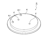
- FIG. 3 is a perspective view showing the stage carriage.
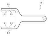
- FIG. 4 is a plan view showing the hand of the transport apparatus.
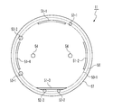
- FIG. 5 is a plan view showing the upper cartridge.
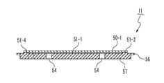
- FIG. 6 is a cross-sectional view showing the upper cartridge.
- FIG. 7 is a cross-sectional view showing the wafer positioning pins.
- FIG. 8 is a cross-sectional view showing a positioning pin.
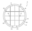
- FIG. 9 is a plan view showing the lower cartridge.
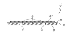
- FIG. 10 is a cross-sectional view showing the lower cartridge.
- FIG. 11 is a cross-sectional view showing a state where the wafer is placed on the cartridge.
- FIG. 12 is a diagram illustrating an operation of transporting the upper wafer.
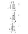
- FIG. 13 is a diagram illustrating an operation of transporting the lower wafer.
- the room-temperature bonding apparatus 1 includes a bonding chamber 2 and a load lock chamber 3 as shown in FIG.
- the joining chamber 2 and the load lock chamber 3 are containers that seal the inside from the environment, and are generally formed of stainless steel, aluminum alloy, or the like.
- the room temperature bonding apparatus 1 further includes a gate valve 5.
- the gate valve 5 is interposed between the bonding chamber 2 and the load lock chamber 3, and closes or opens a gate connecting the inside of the bonding chamber 2 and the load lock chamber 3.
- the load lock chamber 3 includes an upper cartridge base 6, a lower cartridge base 7, and a transfer device 8.
- the upper cartridge 11 is arranged on the upper cartridge base 6.
- the lower cartridge base 7 is provided with the lower cartridge 12.
- the load lock chamber 3 further includes a vacuum pump and a lid (not shown).
- the vacuum pump exhausts gas from the inside of the load lock chamber 3.
- An example of the vacuum pump is a turbo molecular pump that exhausts gas blades by blowing a plurality of metal blades inside.
- the lid can be opened by closing the gate that connects the outside and the inside of the load lock chamber 3 to create an atmospheric atmosphere.
- the size of the gate is larger than that of the upper cartridge 11 and the lower cartridge 12.
- the transfer device 8 includes a first arm 15, a second arm 16, a hand 17, a first node 18, a second node 19, and a third node 20.
- the first arm 15, the second arm 16, and the hand 17 are each formed in a bar shape.
- the first section 18 is supported by the floor plate of the load lock chamber 3 and supports the first arm 15 so as to be rotatable about the rotation shaft 22.
- the rotating shaft 23 is parallel to the vertical direction.
- the second joint 19 is supported by the first joint 18 and supports the second arm 16 so as to be rotatable about the rotation shaft 23.
- the rotating shaft 23 is parallel to the vertical direction, that is, parallel to the rotating shaft 22.
- the third section 20 is supported by the second section 19 and supports the hand 17 so as to be rotatable about the rotation shaft 24.
- the rotating shaft 24 is parallel to the vertical direction, that is, parallel to the rotating shaft 23.
- the transport device 8 further includes an elevating mechanism and a telescopic mechanism that are not shown.
- the raising / lowering mechanism raises / lowers the first arm 15 and raises / lowers the hand 17 by a user operation.
- the telescopic mechanism controls the first joint 18 to rotate the hand 17 and controls the first joint 18, the second joint 19, and the third joint 20 to be parallel to the longitudinal direction of the hand 17 by a user operation. The hand 17 is moved in parallel.
- the transfer device 8 transfers the upper cartridge 11 or the lower cartridge 12 from the load lock chamber 3 to the bonding chamber 2 via the gate valve 5 or from the bonding chamber 2 to the load lock chamber 3 via the gate valve 5. It is used for transporting the upper cartridge 11 or the lower cartridge 12.
- the bonding chamber 2 includes a vacuum pump 31, an ion gun 32, and an electron gun 33.
- the joining chamber 2 has an exhaust port 35 formed in a part of a wall 34 forming a container.
- the vacuum pump 31 is disposed outside the bonding chamber 2 and exhausts gas from the inside of the bonding chamber 2 through the exhaust port 35. Examples of the vacuum pump 31 include a turbo molecular pump that exhausts gas blades by blowing a plurality of metal blades inside.
- the ion gun 32 is arranged facing one irradiation direction 36 and emits charged particles accelerated toward the irradiation direction 36. Argon ions are exemplified as the charged particles.
- the ion gun 32 can be replaced with another surface activation device that activates the surface of the wafer to be bonded.
- the surface activation device include a plasma gun and a fast atom beam source.
- the electron gun 33 is arranged so as to be directed to a target irradiated with charged particles by the ion gun 32, and emits electrons accelerated toward the target.
- the wall 34 is partially formed with a door 37.
- the door 37 includes a hinge 38.
- the hinge 38 supports the door 37 so as to be rotatable with respect to the wall 34.
- the wall 34 further has a window 39 formed in a part thereof.
- the window 39 is formed of a material that transmits visible light without transmitting gas.
- the window 39 may be anywhere on the wall 34 as long as the user can be irradiated with the charged particles by the ion gun 32 or the bonding state can be seen from the outside of the bonding chamber 2.
- the bonding chamber 2 further includes an upper stage 41 and a lower stage 42 therein.
- the lower stage 42 is disposed below the bonding chamber 2.
- the upper stage 41 is disposed above the bonding chamber 2 and includes a sample stage 43-1 and a pressure contact mechanism 43-2.
- the sample stage 43-1 is supported so as to be movable in the vertical direction with respect to the bonding chamber 2.
- the sample stage 43-1 includes a dielectric layer at the lower end, applies a voltage between the dielectric layer and the wafer, and adsorbs the wafer to the dielectric layer by electrostatic force.
- the pressure contact mechanism 43-2 moves the sample stage 43-1 in the vertical direction with respect to the bonding chamber 2 by a user operation.
- the ion gun 32 When the substrate supported by the upper stage 41 and the substrate supported by the lower stage 42 are separated from each other, the ion gun 32 includes a substrate supported by the upper stage 41 and a substrate supported by the lower stage 42. It is directed to the space between. That is, the irradiation direction 36 of the ion gun 32 passes between the substrate supported by the upper stage 41 and the substrate supported by the lower stage 42 and intersects the inner surface of the bonding chamber 2.
- the lower stage 42 includes a stage carriage 45 as shown in FIG.
- the stage carriage 45 is generally formed in a disc shape.
- the stage carriage 45 is arranged so that the axis of the disk is parallel to the vertical direction, and a flat support surface 46 is formed on the upper surface of the disk.
- the stage carriage 45 has a plurality of alignment holes 47 formed in the support surface 46.
- the stage carriage 45 further includes a plurality of positioning pins 48-1 to 48-2 formed on the outer peripheral portion of the support surface 46.
- the plurality of positioning pins 48-1 to 48-2 are each formed in a circular and tapered protrusion.
- the lower stage 42 further includes two imaging devices and a positioning mechanism not shown.
- the imaging device is disposed immediately below the stage carriage 45.
- the imaging device captures an image of a substrate supported by the lower stage 42 through a plurality of alignment holes 47 of the stage carriage 45 by a user operation.
- the positioning mechanism translates the stage carriage 45 in a direction parallel to the horizontal direction and rotates the stage carriage 45 about a rotation axis parallel to the vertical direction by a user operation.
- FIG. 4 shows the hand 17 of the transport device 8.
- the hand 17 has claws 21-1 and 21-2 at the end opposite to the end joined to the third joint 20.
- the claws 21-1 and 21-2 are each formed in a plate shape.
- the claws 21-1 and 21-2 are arranged along one horizontal plane.
- the claw 21-1 has a straight edge 25-1.
- the claw 21-2 has a straight edge 25-2.
- the claws 21-1 and 21-2 are arranged so that the edge 25-1 faces the edge 25-2 and the edges 25-1 and 25-2 are parallel to each other. Yes.
- the claw 21-1 has a notch 49-1 formed in a part of the edge 25-1.
- the claw 21-2 has a notch 49-2 formed in a part of the edge 25-2.
- the notch 49-2 is formed so as to face the notch 49-1.
- FIG. 5 shows the upper cartridge 11.
- the upper cartridge 11 is made of aluminum or stainless steel, is formed in a generally disc shape, and is used for mounting the upper wafer.
- the upper cartridge 11 has a plurality of positioning holes 53-1 to 53-2 and a plurality of alignment holes 54 formed therein.
- the plurality of positioning holes 53-1 to 53-2 are formed in a circular shape and are formed in the vicinity of the outer periphery of the disk.
- the diameters of the plurality of positioning holes 53-1 to 53-2 are approximately equal to the diameters of the positioning pins 48-1 to 48-2 of the stage carriage 45, respectively.
- the plurality of positioning holes 53-1 to 53-2 are further arranged so that the distance between the positioning hole 53-1 and the positioning hole 53-2 matches the distance between the positioning pin 48-1 and the positioning pin 48-2.
- the plurality of positioning holes 53-1 to 53-2 are arranged so as to be fitted to the plurality of positioning pins 48-1 to 48-2 when the upper cartridge 11 is placed on the stage carriage 45. . That is, when the upper cartridge 11 is placed on the stage carriage 45 so that the plurality of positioning pins 48-1 to 48-2 fit into the plurality of positioning holes 53-1 to 53-2, the stage carriage 45 is fixed. Placed in position.
- the plurality of alignment holes 54 are formed so as to penetrate therethrough.
- the plurality of alignment holes 54 are formed so as to be respectively connected to the plurality of alignment holes 47 of the stage carriage 45 when the upper cartridge 11 is placed on the stage carriage 45.
- the plurality of alignment holes 54 are further formed so as to coincide with alignment marks formed on the upper wafer when the upper wafer is placed on the upper cartridge 11.
- the two imaging devices of the lower stage 42 are arranged so that the alignment mark can be photographed through the plurality of alignment holes 54 when the upper cartridge 11 is placed on the stage carriage 45. .
- the upper cartridge 11 further includes a plurality of island portions 51-1 to 51-4 and a plurality of wafer positioning pins 52-1 to 52-3 formed on the upper surface of the disk.
- the plurality of island portions 51-1 to 51-4 are formed on a protrusion protruding from the upper surface of the disk, are formed along the outer periphery of the upper wafer placed on the upper cartridge 11, and the upper end is on one plane. It is formed along.
- the plurality of wafer positioning pins 52-1 to 52-3 are formed on the protrusions protruding from the upper surface of the disk, and are formed along the outer periphery of the upper wafer placed on the upper cartridge 11.
- Wafer positioning pins 52-2 to 52-3 are formed along the oriental flat of the upper wafer mounted on upper cartridge 11 in particular.
- the cartridge 11 is placed at a fixed position.
- the upper cartridge 11 further includes a plurality of islands so that a space between the upper cartridge 11 and the upper wafer 50-1 is communicated to the outside when the upper wafer is placed in its fixed position. Portions 51-1 to 51-4 are formed. That is, the plurality of island portions 51-1 to 51-4 are formed so as not to be connected to each other.
- the plurality of wafer positioning pins 52-1 to 52-3 are formed higher than the plurality of island portions 51-1 to 51-4, and the heights of the plurality of island portions 51-1 to 51-4 and the upper wafers are increased. It is formed lower than the sum of the thickness. That is, as shown in FIG. 6, when the upper wafer 50-1 is placed on the upper cartridge 11, the plurality of island portions 51-1 to 51-4 are arranged on the upper cartridge 11 of the upper wafer 50-1. Is formed so as to be in contact with the outer periphery of the surface facing the.
- the plurality of wafer positioning pins 52-1 to 52-3 are formed so as to contact the side surface of the upper wafer 50-1 when the upper wafer 50-1 is placed on the upper cartridge 11. When the upper wafer 50-1 is placed on the upper cartridge 11, the plurality of wafer positioning pins 52-1 to 52-3 do not protrude from the back surface of the surface facing the upper cartridge 11 of the upper wafer 50-1. Is formed.
- the upper cartridge 11 is formed of a flange portion 56 and a main body portion 57 as shown in FIG.
- the main body portion 57 is formed in a columnar shape.
- the diameter of the cylinder is smaller than the distance between the side edge 25-1 and the side edge 25-2 of the hand 17.
- the flange portion 56 is formed so as to protrude from the side surface of the cylinder of the main body portion 57 and is formed in a disk shape.
- the diameter of the disk is larger than the distance between the hand 17 edge 25-1 and edge 25-2. That is, the upper cartridge 11 is gripped by the transport device 8 when the flange portion 56 is placed on the claws 21-1 to 21-2.
- the upper cartridge 11 is further formed with positioning pins 59 as shown in FIG.
- the positioning pin 59 is formed as a protrusion protruding from the surface facing the lower side of the flange portion 56.
- the diameter of the positioning pin 59 is substantially equal to the diameter of the notches 49-1 to 49-2.
- Two positioning pins 59 are formed in two portions that are symmetrical with respect to the center of the disk of the flange portion 56. That is, the positioning pins 59 are formed so as to be fitted into the notches 49-1 to 49-2 of the claws 21-1 to 21-2 when the upper cartridge 11 is gripped by the transport device 8, respectively. Yes.
- the upper cartridge 11 is gripped at a fixed position of the hand 17 when being gripped by the transport device 8 so as to be fitted into the notches 49-1 to 49-2 of the claws 21-1 to 21-2, respectively.
- the positioning pin 59 is formed as a protrusion protruding from the surface facing the lower side of the flange portion 56.
- FIG. 9 shows the lower cartridge 12.
- the lower cartridge 12 is formed of aluminum, is formed in a generally disc shape, and is used for mounting the lower wafer.
- the lower cartridge 12 has a plurality of positioning holes 63-1 and 63-2 and a plurality of alignment holes 64 formed therein.
- the plurality of positioning holes 63-1 to 63-2 are formed in a circular shape and are formed in the vicinity of the outer periphery of the disk.
- the diameters of the plurality of positioning holes 63-1 to 63-2 are approximately equal to the diameters of the positioning pins 48-1 to 48-2 of the stage carriage 45, respectively.
- the plurality of positioning holes 63-1 to 63-2 are further arranged so that the distance between the positioning hole 63-1 and the positioning hole 63-2 matches the distance between the positioning pin 48-1 and the positioning pin 48-2. Is formed. That is, the plurality of positioning holes 63-1 to 63-2 are arranged so as to be fitted to the plurality of positioning pins 48-1 to 48-2 when the lower cartridge 12 is placed on the stage carriage 45. Yes. That is, when the lower cartridge 12 is placed on the stage carriage 45 so that the plurality of positioning pins 48-1 to 48-2 fit into the plurality of positioning holes 63-1 to 63-2, Can be placed in place.
- the plurality of alignment holes 64 are formed so as to penetrate therethrough.
- the plurality of alignment holes 64 are formed so as to be respectively connected to the plurality of alignment holes 47 of the stage carriage 45 when the lower cartridge 12 is placed on the stage carriage 45. Further, the plurality of alignment holes 64 are formed so as to coincide with the alignment mark formed on the lower wafer when the lower wafer is placed on the lower cartridge 12.
- the two imaging devices of the lower stage 42 are arranged so that the alignment mark can be photographed through the plurality of alignment holes 64 when the lower cartridge 12 is placed on the stage carriage 45. Yes.
- the lower cartridge 12 further has an island portion 61 and a plurality of wafer positioning pins 62-1 to 62-3 formed on the upper surface of the disk.
- the island portion 61 is formed in a protrusion protruding from the upper surface of the disk, is formed in a shape substantially equal to the shape of the lower wafer placed on the lower cartridge 12, and is formed so that the upper end is along one plane. ing.
- the island portion 61 has a groove 65 formed at the upper end.
- the grooves 65 are formed in a lattice shape at the upper end.
- the groove 65 is further formed so as to be connected to the side surface of the island portion 61.
- the plurality of wafer positioning pins 62-1 to 62-3 are formed on the protrusions protruding from the upper surface of the disk, and are formed along the outer periphery of the lower wafer placed on the lower cartridge 12.
- Wafer positioning pins 62-2 to 62-3 are particularly formed along the oriental flat of the lower wafer placed on lower cartridge 12. At this time, when the lower wafer is placed on the lower cartridge 12 such that the oriental flat is in contact with the wafer positioning pins 62-2 to 62-3 and the outer periphery thereof is in contact with the wafer positioning pins 62-1.
- the lower cartridge 12 is placed at a fixed position.
- the plurality of wafer positioning pins 62-1 to 62-3 are formed higher than the island portion 61, and are formed lower than the sum of the height of the island portion 61 and the thickness of the lower wafer. That is, the island portion 61 is formed so as to contact most of the surface facing the lower cartridge 12 of the lower wafer when the lower wafer is placed on the lower cartridge 12.
- the plurality of wafer positioning pins 62-1 to 62-3 are formed so as to come into contact with the side surface of the lower wafer when the lower wafer is placed on the lower cartridge 12.
- the plurality of wafer positioning pins 62-1 to 62-3 do not protrude from the back surface of the surface facing the lower cartridge 12 of the lower wafer when the lower wafer is placed on the lower cartridge 12. Is formed.
- the lower cartridge 12 is formed of a flange portion 66 and a main body portion 67 as shown in FIG.
- the main body portion 67 is formed in a cylindrical shape.
- the diameter of the cylinder is smaller than the distance between the edge 25-1 and the edge 25-2.
- the flange portion 66 is formed so as to protrude from the cylindrical side surface of the main body portion 67 and is formed in a disc shape.
- the diameter of the disk is larger than the distance between the edge 25-1 and the edge 25-2. That is, the lower cartridge 12 is gripped by the transport device 8 when the flange portion 66 is placed on the claws 21-1 to 21-2.
- the lower cartridge 12 is further provided with positioning pins in the same manner as the upper cartridge 11.
- the positioning pin is formed as a protrusion protruding from the surface facing the lower side of the flange portion 66.
- the diameter of the positioning pin is substantially equal to the diameter of the notches 49-1 to 49-2.
- Two of the positioning pins are formed in two portions which are symmetrical with respect to the center of the disk of the flange portion 66. That is, the positioning pins are formed so as to fit into the notches 49-1 to 49-2 of the claws 21-1 to 21-2 when the lower cartridge 12 is gripped by the transport device 8, respectively. ing.
- the lower cartridge 12 is held at a fixed position of the hand 17 when being held by the transport device 8 so as to be fitted into the notches 49-1 to 49-2 of the claws 21-1 to 21-2, respectively. Is done.
- the upper cartridge base 6 and the lower cartridge base 7 are formed with a plurality of positioning pins similar to the plurality of positioning pins 48-1 to 48-2 in the same manner as the stage carriage 45. That is, when the upper cartridge 11 is placed on the upper cartridge base 6 so that the plurality of positioning pins of the upper cartridge base 6 are fitted in the plurality of positioning holes 53-1 to 53-2, the upper cartridge base 6 is fixed. Placed in position. When the lower cartridge 12 is placed on the lower cartridge base 7 so that the plurality of positioning pins of the lower cartridge base 7 fit into the plurality of positioning holes 63-1 to 63-2, the lower cartridge base 7 It is placed in the fixed position.
- the embodiment of the room temperature bonding method according to the present invention is executed using the room temperature bonding apparatus 1.
- the operator first closes the gate valve 5, generates a vacuum atmosphere inside the bonding chamber 2 using the vacuum pump 31, and generates an atmospheric pressure atmosphere inside the load lock chamber 3.
- the operator opens the lid of the load lock chamber 3, places the upper cartridge 11 on the upper cartridge base 6, and places the lower cartridge 12 on the lower cartridge base 7.
- the operator places the upper wafer on the upper cartridge 11 so that the oriental flat is in contact with the wafer positioning pins 52-2 to 52-3 and the outer periphery is in contact with the wafer positioning pins 52-1.
- the operator places the lower wafer 50-2 on the lower cartridge 12 so that the oriental flat contacts the wafer positioning pins 62-2 to 62-3 and the outer periphery contacts the wafer positioning pins 62-1. .
- the operator closes the lid of the load lock chamber 3 to generate a vacuum atmosphere inside the load lock chamber 3.
- the wafer 70 exemplified by the upper wafer 50-1 and the lower wafer 50-2 may be deformed as shown in FIG.
- a space 72 is formed between the wafer 70 and the cartridge 71.
- the air filled in the space 72 may lift the wafer 70 and move the wafer 70 over the cartridge 71.
- the gas filled in the space between the upper cartridge 11 and the upper wafer 50-1 is exhausted to the outside through the gaps between the plurality of island portions 51-1 to 51-4.
- Such exhaust prevents the gas sandwiched between the upper cartridge 11 and the upper wafer 50-1 from lifting the upper wafer 50-1, and prevents the upper wafer 50-1 from moving on the upper cartridge 11.
- the gas filled in the space sandwiched between the lower cartridge 12 and the lower wafer 50-2 is exhausted to the outside through the groove 65.
- Such exhaust prevents the gas sandwiched between the lower cartridge 12 and the lower wafer 50-2 from lifting the lower wafer 50-2, and the lower wafer 50-2 is located above the lower cartridge 12. Prevent moving.
- FIG. 12 shows an operation of holding the upper wafer 50-1 on the sample stage 43-1.
- the operator uses the transfer device 8 to move the upper cartridge 11 on which the upper wafer 50-1 is placed from the upper cartridge base 6 to the stage carriage 45. Transport. The worker lowers the hand 17 of the transport device 8 as shown in FIG. At this time, in the upper cartridge 11, the plurality of positioning holes 53-1 to 53-2 are fitted into the plurality of positioning pins 48-1 to 48-2 of the stage carriage 45, respectively, and are held by the stage carriage 45.
- the operator lowers the sample stage 43-1 vertically downward to bring the dielectric layer of the sample stage 43-1 into contact with the upper wafer 50-1, and the upper wafer 50-1 is placed on the sample stage 43-1. Hold.
- the plurality of wafer positioning pins 52-1 to 52-3 of the upper cartridge 11 are formed so as not to protrude from the upper wafer 50-1, they do not contact the sample stage 43-1.
- the room temperature bonding apparatus 1 can more reliably bring the upper wafer 50-1 into contact with the sample stage 43-1 and can more reliably hold the upper wafer 50-1 on the sample stage 43-1. .
- the operator raises the sample stage 43-1 vertically upward to separate the upper wafer 50-1 from the upper cartridge 11.
- the operator uses the transfer device 8 to transfer the upper cartridge 11 on which the upper wafer 50-1 is not placed from the stage carriage 45 to the upper cartridge base 6. To do.
- FIG. 13 shows an operation for holding the lower wafer 50-2 on the stage carriage 45.
- the operator uses the transfer device 8 to move the lower cartridge 12 on which the lower wafer 50-2 is placed from the lower cartridge base 7 to the stage carriage 45. To the top.
- the worker lowers the hand 17 of the transport device 8 as shown in FIG.
- the plurality of positioning holes 63-1 to 63-2 are fitted into the plurality of positioning pins 48-1 to 48-2 of the stage carriage 45, respectively, and are held by the stage carriage 45.
- the operator retreats the hand 17 of the transfer device 8 into the load lock chamber 3 as shown in FIG.
- the operator closes the gate valve 5 and joins the upper wafer 50-1 held on the sample stage 43-1 and the lower wafer 50-2 held on the stage carriage 45 at room temperature. That is, the operator moves the upper wafer 50-1 and lower wafer 50-1 while the upper wafer 50-1 held by the sample stage 43-1 and the lower wafer 50-2 held by the stage carriage 45 are separated from each other.
- the ion gun 32 is directed between 50-2 and the particles are discharged. The particles are irradiated to the upper wafer 50-1 and the lower wafer 50-2, and oxides and the like formed on the surfaces are removed, and impurities adhering to the surfaces are removed.
- the operator operates the press-contact mechanism 43-2 to lower the sample stage 43-1 vertically downward to bring the upper wafer 50-1 and the lower wafer 50-2 closer to each other.
- the operator operates the positioning mechanism of the stage carriage 45 so that the upper wafer 50-1 and the lower wafer 50-2 are bonded as designed so that the lower wafer 50- held by the stage carriage 45 is bonded.
- Move position 2 The operator operates the pressure contact mechanism 43-2 of the sample stage 43-1 to lower the sample stage 43-1 vertically downward to bring the upper wafer 50-1 into contact with the lower wafer 50-2.
- the upper wafer 50-1 and the lower wafer 50-2 are bonded by the contact, and one bonded substrate is generated.
- the room temperature bonding apparatus 1 can more reliably contact the lower wafer 50-2 with the upper wafer 50-1, and more reliably bond the upper wafer 50-1 and the lower wafer 50-2. be able to. Further, at this time, the island portion 61 of the lower cartridge 12 contacts almost the entire lower wafer 50-2. Therefore, the lower wafer 50-2 is prevented from being damaged by a load applied during bonding, and the room temperature bonding apparatus 1 applies a larger load to the upper wafer 50-1 and the lower wafer 50-2. Can be applied.
- the operator dechucks the bonded substrate from the sample stage 43-1 and then raises the sample stage 43-1 vertically upward.
- the operator opens the gate valve 5 and uses the transfer device 8 to transfer the lower cartridge 12 on which the bonded substrate is placed from the stage carriage 45 to the lower cartridge base 7.
- the operator closes the gate valve 5 to generate an atmospheric pressure atmosphere inside the load lock chamber 3.
- the operator opens the lid of the load lock chamber 3 and takes out the bonded substrate from the lower cartridge 12 arranged on the lower cartridge base 7.
- the upper wafer 50-1 and the lower wafer 50-2 are not brought into contact with the transfer device 8, and contamination of the bonding surface can be prevented and the room temperature bonding can be performed more reliably. it can. As a result, the reliability of the room temperature bonding apparatus 1 is further improved.
- the wafer delivery between the stage for room temperature bonding and the transfer apparatus is generally performed using lift pins arranged in the bonding chamber.
- the room temperature bonding apparatus 1 does not need to include such a lift pin, can reduce the manufacturing cost, and can reduce maintenance.
- the drive system that drives the object generally releases gas and contaminates the atmosphere within the chamber when placed in the chamber.
- the room temperature bonding apparatus 1 does not include a drive system for driving the lift pins, it is possible to reduce such emitted gas and prevent contamination of the atmosphere in which the wafer is bonded.
- the room temperature bonding apparatus 1 can prevent the contamination of the bonding surface between the upper wafer 50-1 and the lower wafer 50-2, can perform the room temperature bonding more reliably, and further improve the reliability.
- the wafer may be deformed, dropped and damaged when directly held by the transfer device 8.
- the lower wafer 50-2 is conveyed by being held by the lower cartridge 12 with almost the entire one surface contacting the lower cartridge 12, and being deformed, dropped, or damaged. The fear can be reduced. As a result, the room temperature bonding apparatus 1 can perform room temperature bonding more reliably, and the reliability is further improved.
- the upper wafer 50-1 can be replaced with a deformed wafer formed in a shape different from the disk shape.
- the upper cartridge 11 can place the deformed wafer so that the deformed wafer does not move during decompression.
- the room temperature bonding apparatus 1 can prevent contamination of the bonding surface of the deformed wafer and more reliably bond the deformed wafer at room temperature.
- the lower cartridge 12 can be manufactured for each of the irregular wafers.
- the lower wafer 50-2 can be replaced with a deformed wafer formed in a shape different from a disk shape.
- the lower cartridge 12 can place the deformed wafer so that the deformed wafer does not move during decompression.
- the room temperature bonding apparatus 1 can prevent contamination of the bonding surface of the deformed wafer and more reliably bond the deformed wafer at room temperature.
- the lower cartridge 12 can be manufactured for each of the irregular wafers. At this time, the room temperature bonding apparatus 1 does not need to produce the stage carriage 45 for each of the irregular wafers, and can be produced at a lower cost.
- the groove 65 formed in the lower cartridge 12 may be formed in another shape different from the lattice shape.
- the shape is exemplified by a radial shape.
- the grooves 65 are preferably numerous and thick in order to improve the efficiency of exhausting the gas sandwiched between the lower cartridge 12 and the lower wafer 50-2.
- the groove 65 is preferably thin and preferably a small number in order to cause deformation of the lower wafer 50-2 when the upper wafer 50-1 and the lower wafer 50-2 are bonded. Therefore, it is preferable that the shape of the groove 65 is appropriately designed according to the attribute of the lower wafer 50-2.
Landscapes
- Engineering & Computer Science (AREA)
- Mechanical Engineering (AREA)
- Container, Conveyance, Adherence, Positioning, Of Wafer (AREA)
- Pressure Welding/Diffusion-Bonding (AREA)
Abstract
Description
本発明の他の課題は、接合される基板の汚染を防止する常温接合装置を提供することにある。
本発明のさらに他の課題は、基板が接合される雰囲気の汚染を防止する常温接合装置を提供することにある。
本発明のさらに他の課題は、製造コストがより小さい常温接合装置を提供することにある。
本発明のさらに他の課題は、メンテナンスが軽減される常温接合装置を提供することにある。
本発明のさらに他の課題は、接合される基板の破損を防止する常温接合装置を提供することにある。
本発明のさらに他の課題は、より薄い基板を搬送・接合することに好適である常温接合装置を提供することにある。
本発明のさらに他の課題は、様々な形状の基板を搬送・接合することに好適である常温接合装置を提供することにある。
本発明による常温接合装置は、さらに、搬送装置が基板に直接に接触することなく、基板を搬送することができ、接合される基板の汚染を防止することができる。
本発明による常温接合装置は、さらに、基板が接合される雰囲気の汚染を防止することができる。
本発明による常温接合装置は、さらに、製造コストがより小さくすることができる。
本発明による常温接合装置は、さらに、メンテナンスを軽減することができる。
本発明による常温接合装置は、さらに、接合される基板の破損を防止することができる。
本発明による常温接合装置は、さらに、より薄い基板を搬送・接合することに好適である。
本発明による常温接合装置は、さらに、様々な形状の基板を搬送・接合することに好適である。
Claims (14)
- 内部の雰囲気が減圧されるロードロックチャンバーと、
前記ロードロックチャンバーの内部に配置されるカートリッジとを具備し、
前記カートリッジは、前記基板が前記カートリッジに載せられるときに前記基板に接触する島部分が形成され、
前記島部分は、前記基板が載せられているときに前記カートリッジと前記基板とに挟まれる空間を外部に接続する流路が形成されている
常温接合装置。 - 請求の範囲1において、
接合チャンバーと、
前記ロードロックチャンバーと前記接合チャンバーとのゲートを開閉するゲートバルブと、
前記ゲートが開放されているときに前記ロードロックチャンバーから前記接合チャンバーに前記カートリッジを搬送する搬送装置とを更に具備し、
前記接合チャンバーは、前記基板が前記接合チャンバーの内部に配置されているときに、前記基板を他の基板に接合する
常温接合装置。 - 請求の範囲2において、
前記カートリッジは、フランジが形成され、
前記搬送装置は、前記フランジのうちの下向きの支持面に接触することにより、前記カートリッジを保持する
常温接合装置。 - 請求の範囲3において、
前記カートリッジは、前記フランジにハンド位置決め手段が形成され、
前記搬送装置は、前記カートリッジを搬送するときに、前記ハンド位置決め手段に嵌合する他のハンド位置決め手段が形成されている
常温接合装置。 - 請求の範囲4において、
前記ハンド位置決め手段は、ピンであり、
前記他のハンド位置決め手段は、切り欠きである
常温接合装置。 - 請求の範囲2~請求の範囲5のいずれかにおいて、
前記接合チャンバーは、前記カートリッジを保持する下側ステージを備え、
前記カートリッジは、ステージ位置決め手段が形成され、
前記下側ステージは、前記下側ステージが前記カートリッジを保持するときに、前記ステージ位置決め手段に嵌合する他のステージ位置決め手段が形成されている
常温接合装置。 - 請求の範囲6において、
前記ステージ位置決め手段は、孔であり、
前記他のステージ位置決め手段は、前記孔に嵌まる突起である
常温接合装置。 - 請求の範囲6または請求の範囲7のいずれかにおいて、
撮影装置と、
アライメント装置とを更に具備し、
前記カートリッジは、アライメント用孔が形成され、
前記撮影装置は、前記基板が前記カートリッジに載せられる場合で、前記下側ステージが前記カートリッジを保持しているときに、前記アライメント用孔を介して前記基板の画像を撮影し、
前記アライメント装置は、前記画像に基づいて前記下側ステージを駆動する
常温接合装置。 - 請求の範囲8において、
前記島部分は、前記基板の一方の面の概ね全部に接触する接触面が形成され、
前記接触面には、前記流路である溝が形成されている
常温接合装置。 - 請求の範囲1~請求の範囲9のいずれかにおいて、
前記カートリッジは、複数の基板位置決めピンを備え、
前記複数の基板位置決めピンは、前記基板が前記カートリッジに載せられたときに、前記基板の縁が前記複数の基板位置決めピンの全部に接触するように、配置されている
常温接合装置。 - 請求の範囲10において、
前記複数の基板位置決めピンは、前記基板が前記カートリッジに載せられたときに、前記基板の表面のうちの前記カートリッジに接触する面と前記面の裏面との間に前記複数の基板位置決めピンの先端が配置されるように、形成されている
常温接合装置。 - 請求の範囲1~請求の範囲7のいずれかにおいて、
前記島部分は、前記基板の一方の面の中央部分に接触しないで、前記基板の一方の面の外周部分に接触する
常温接合装置。 - 基板が載せられているカートリッジが配置されているロードロックチャンバーの内部を減圧するステップと、
前記ロードロックチャンバーの内部が減圧された後に、前記ロードロックチャンバーの内部から接合チャンバーに前記カートリッジを搬送するステップとを具備し、
前記カートリッジは、前記基板が前記カートリッジに載せられるときに前記基板に接触する島部分が形成され、
前記島部分は、前記基板が載せられているときに前記カートリッジと前記基板とに挟まれる空間を外部に接続する流路が形成されている
常温接合方法。 - 請求の範囲13において、
前記接合チャンバーは、上側ステージと下側ステージとを備え、
前記基板は、上側基板と下側基板とを含み、
前記カートリッジは、上側カートリッジと下側カートリッジとを含み、
さらに、
前記上側基板が前記上側カートリッジに載せられている場合で、かつ、前記下側ステージが前記上側カートリッジを保持しているときに、前記上側ステージと前記下側ステージとを接近させることにより前記上側基板を前記上側ステージに保持させるステップと、
前記上側基板が前記上側ステージに保持された後に、前記下側基板が前記下側カートリッジに載せられている場合で、かつ、前記下側ステージが前記下側カートリッジを保持しているときに、前記上側ステージと前記下側ステージとを接近させることにより前記上側基板と前記下側基板とを接合するステップ
とを具備する常温接合方法。
Priority Applications (4)
| Application Number | Priority Date | Filing Date | Title |
|---|---|---|---|
| US13/139,085 US8906175B2 (en) | 2008-12-11 | 2009-09-29 | Room temperature bonding apparatus |
| CA2746035A CA2746035C (en) | 2008-12-11 | 2009-09-29 | Room temperature bonding apparatus |
| KR1020117013321A KR101252974B1 (ko) | 2008-12-11 | 2009-09-29 | 상온 접합 장치 |
| CN200980149748.5A CN102246266B (zh) | 2008-12-11 | 2009-09-29 | 常温接合装置 |
Applications Claiming Priority (2)
| Application Number | Priority Date | Filing Date | Title |
|---|---|---|---|
| JP2008-315431 | 2008-12-11 | ||
| JP2008315431A JP4796120B2 (ja) | 2008-12-11 | 2008-12-11 | 常温接合装置 |
Publications (1)
| Publication Number | Publication Date |
|---|---|
| WO2010067656A1 true WO2010067656A1 (ja) | 2010-06-17 |
Family
ID=42242648
Family Applications (1)
| Application Number | Title | Priority Date | Filing Date |
|---|---|---|---|
| PCT/JP2009/066990 Ceased WO2010067656A1 (ja) | 2008-12-11 | 2009-09-29 | 常温接合装置 |
Country Status (7)
| Country | Link |
|---|---|
| US (1) | US8906175B2 (ja) |
| JP (1) | JP4796120B2 (ja) |
| KR (1) | KR101252974B1 (ja) |
| CN (1) | CN102246266B (ja) |
| CA (1) | CA2746035C (ja) |
| TW (1) | TWI423374B (ja) |
| WO (1) | WO2010067656A1 (ja) |
Families Citing this family (3)
| Publication number | Priority date | Publication date | Assignee | Title |
|---|---|---|---|---|
| JP6014302B2 (ja) * | 2010-09-06 | 2016-10-25 | 東京応化工業株式会社 | 貼り合わせ装置および貼り合わせ方法 |
| JP6165127B2 (ja) * | 2014-12-22 | 2017-07-19 | 三菱重工工作機械株式会社 | 半導体装置及び半導体装置の製造方法 |
| TWI783714B (zh) * | 2021-05-10 | 2022-11-11 | 環球晶圓股份有限公司 | 晶圓接合設備 |
Citations (8)
| Publication number | Priority date | Publication date | Assignee | Title |
|---|---|---|---|---|
| JPH04282848A (ja) * | 1991-03-12 | 1992-10-07 | Fujitsu Ltd | 半導体装置の製造装置 |
| JPH07201948A (ja) * | 1993-12-29 | 1995-08-04 | Dainippon Screen Mfg Co Ltd | 基板搬送治具 |
| JPH11329983A (ja) * | 1998-05-12 | 1999-11-30 | Sumitomo Metal Ind Ltd | Cvdによる成膜方法とその装置 |
| JP2005142537A (ja) * | 2003-10-15 | 2005-06-02 | Bondotekku:Kk | 縦振接合方法及び装置 |
| JP2007012942A (ja) * | 2005-06-30 | 2007-01-18 | Canon Inc | 容器及びそれを使って基板を搬送する方法 |
| JP2007265971A (ja) * | 2006-02-28 | 2007-10-11 | Sii Nanotechnology Inc | ウエハホルダ、試料作製装置 |
| JP2007329238A (ja) * | 2006-06-07 | 2007-12-20 | Shin Etsu Polymer Co Ltd | ウェーハ収納容器 |
| JP2008235460A (ja) * | 2007-03-19 | 2008-10-02 | Sii Nanotechnology Inc | ウエハ搬送機構、ウエハ保持機構、及び、試料作製装置 |
Family Cites Families (5)
| Publication number | Priority date | Publication date | Assignee | Title |
|---|---|---|---|---|
| JP4822577B2 (ja) * | 2000-08-18 | 2011-11-24 | 東レエンジニアリング株式会社 | 実装方法および装置 |
| JP2004207606A (ja) | 2002-12-26 | 2004-07-22 | Disco Abrasive Syst Ltd | ウェーハサポートプレート |
| JP4878109B2 (ja) | 2004-08-24 | 2012-02-15 | 株式会社アルバック | 基板移載システムおよび基板移載方法 |
| JP4107316B2 (ja) * | 2005-09-02 | 2008-06-25 | 株式会社日立プラントテクノロジー | 基板貼合装置 |
| JP3970304B1 (ja) * | 2006-03-27 | 2007-09-05 | 三菱重工業株式会社 | 常温接合装置 |
-
2008
- 2008-12-11 JP JP2008315431A patent/JP4796120B2/ja active Active
-
2009
- 2009-09-29 KR KR1020117013321A patent/KR101252974B1/ko active Active
- 2009-09-29 US US13/139,085 patent/US8906175B2/en active Active
- 2009-09-29 CN CN200980149748.5A patent/CN102246266B/zh active Active
- 2009-09-29 WO PCT/JP2009/066990 patent/WO2010067656A1/ja not_active Ceased
- 2009-09-29 CA CA2746035A patent/CA2746035C/en not_active Expired - Fee Related
- 2009-09-30 TW TW098133318A patent/TWI423374B/zh active
Patent Citations (8)
| Publication number | Priority date | Publication date | Assignee | Title |
|---|---|---|---|---|
| JPH04282848A (ja) * | 1991-03-12 | 1992-10-07 | Fujitsu Ltd | 半導体装置の製造装置 |
| JPH07201948A (ja) * | 1993-12-29 | 1995-08-04 | Dainippon Screen Mfg Co Ltd | 基板搬送治具 |
| JPH11329983A (ja) * | 1998-05-12 | 1999-11-30 | Sumitomo Metal Ind Ltd | Cvdによる成膜方法とその装置 |
| JP2005142537A (ja) * | 2003-10-15 | 2005-06-02 | Bondotekku:Kk | 縦振接合方法及び装置 |
| JP2007012942A (ja) * | 2005-06-30 | 2007-01-18 | Canon Inc | 容器及びそれを使って基板を搬送する方法 |
| JP2007265971A (ja) * | 2006-02-28 | 2007-10-11 | Sii Nanotechnology Inc | ウエハホルダ、試料作製装置 |
| JP2007329238A (ja) * | 2006-06-07 | 2007-12-20 | Shin Etsu Polymer Co Ltd | ウェーハ収納容器 |
| JP2008235460A (ja) * | 2007-03-19 | 2008-10-02 | Sii Nanotechnology Inc | ウエハ搬送機構、ウエハ保持機構、及び、試料作製装置 |
Also Published As
| Publication number | Publication date |
|---|---|
| JP4796120B2 (ja) | 2011-10-19 |
| TWI423374B (zh) | 2014-01-11 |
| KR101252974B1 (ko) | 2013-04-15 |
| CN102246266B (zh) | 2014-12-10 |
| JP2010141092A (ja) | 2010-06-24 |
| US20110277904A1 (en) | 2011-11-17 |
| KR20110094053A (ko) | 2011-08-19 |
| CA2746035A1 (en) | 2010-06-17 |
| TW201029095A (en) | 2010-08-01 |
| US8906175B2 (en) | 2014-12-09 |
| CN102246266A (zh) | 2011-11-16 |
| CA2746035C (en) | 2015-04-28 |
Similar Documents
| Publication | Publication Date | Title |
|---|---|---|
| US8857487B2 (en) | Room temperature bonding apparatus | |
| JP5733300B2 (ja) | 基板分離方法、半導体装置の製造方法、基板分離装置、ロードロック装置、及び、基板貼り合わせ装置 | |
| TWI529848B (zh) | 接合裝置及接合加工方法 | |
| JP3970304B1 (ja) | 常温接合装置 | |
| JP4831842B2 (ja) | 接合装置制御装置および多層接合方法 | |
| JP4796182B2 (ja) | ウェハ接合装置 | |
| WO2012043054A1 (ja) | 常温接合装置および常温接合方法 | |
| CN105612598A (zh) | 吸附台、贴合装置以及贴合基板的制造方法 | |
| JP4796120B2 (ja) | 常温接合装置 | |
| JP4859895B2 (ja) | 常温接合装置 | |
| JP2013051358A (ja) | 常温接合装置および常温接合方法 | |
| JP4875678B2 (ja) | 常温接合装置 | |
| JP5448755B2 (ja) | 接合装置 | |
| JP4875676B2 (ja) | 常温接合装置 | |
| JP4875677B2 (ja) | 常温接合装置 | |
| TWI423364B (zh) | 晶圓接合裝置 |
Legal Events
| Date | Code | Title | Description |
|---|---|---|---|
| WWE | Wipo information: entry into national phase |
Ref document number: 200980149748.5 Country of ref document: CN |
|
| 121 | Ep: the epo has been informed by wipo that ep was designated in this application |
Ref document number: 09831762 Country of ref document: EP Kind code of ref document: A1 |
|
| WWE | Wipo information: entry into national phase |
Ref document number: 2746035 Country of ref document: CA |
|
| ENP | Entry into the national phase |
Ref document number: 20117013321 Country of ref document: KR Kind code of ref document: A |
|
| NENP | Non-entry into the national phase |
Ref country code: DE |
|
| WWE | Wipo information: entry into national phase |
Ref document number: 13139085 Country of ref document: US |
|
| 122 | Ep: pct application non-entry in european phase |
Ref document number: 09831762 Country of ref document: EP Kind code of ref document: A1 |