WO2010067649A1 - 可変インダクタ - Google Patents
可変インダクタ Download PDFInfo
- Publication number
- WO2010067649A1 WO2010067649A1 PCT/JP2009/065563 JP2009065563W WO2010067649A1 WO 2010067649 A1 WO2010067649 A1 WO 2010067649A1 JP 2009065563 W JP2009065563 W JP 2009065563W WO 2010067649 A1 WO2010067649 A1 WO 2010067649A1
- Authority
- WO
- WIPO (PCT)
- Prior art keywords
- coil
- magnetic
- variable inductor
- core
- magnetic core
- Prior art date
- Legal status (The legal status is an assumption and is not a legal conclusion. Google has not performed a legal analysis and makes no representation as to the accuracy of the status listed.)
- Ceased
Links
Images



Classifications
-
- H—ELECTRICITY
- H01—ELECTRIC ELEMENTS
- H01F—MAGNETS; INDUCTANCES; TRANSFORMERS; SELECTION OF MATERIALS FOR THEIR MAGNETIC PROPERTIES
- H01F21/00—Variable inductances or transformers of the signal type
- H01F21/02—Variable inductances or transformers of the signal type continuously variable, e.g. variometers
- H01F21/06—Variable inductances or transformers of the signal type continuously variable, e.g. variometers by movement of core or part of core relative to the windings as a whole
-
- H—ELECTRICITY
- H01—ELECTRIC ELEMENTS
- H01F—MAGNETS; INDUCTANCES; TRANSFORMERS; SELECTION OF MATERIALS FOR THEIR MAGNETIC PROPERTIES
- H01F21/00—Variable inductances or transformers of the signal type
- H01F21/02—Variable inductances or transformers of the signal type continuously variable, e.g. variometers
- H01F21/10—Variable inductances or transformers of the signal type continuously variable, e.g. variometers by means of a movable shield
-
- H—ELECTRICITY
- H01—ELECTRIC ELEMENTS
- H01F—MAGNETS; INDUCTANCES; TRANSFORMERS; SELECTION OF MATERIALS FOR THEIR MAGNETIC PROPERTIES
- H01F27/00—Details of transformers or inductances, in general
- H01F27/34—Special means for preventing or reducing unwanted electric or magnetic effects, e.g. no-load losses, reactive currents, harmonics, oscillations, leakage fields
- H01F27/36—Electric or magnetic shields or screens
-
- H—ELECTRICITY
- H01—ELECTRIC ELEMENTS
- H01F—MAGNETS; INDUCTANCES; TRANSFORMERS; SELECTION OF MATERIALS FOR THEIR MAGNETIC PROPERTIES
- H01F29/00—Variable transformers or inductances not covered by group H01F21/00
- H01F29/08—Variable transformers or inductances not covered by group H01F21/00 with core, coil, winding, or shield movable to offset variation of voltage or phase shift, e.g. induction regulators
- H01F29/12—Variable transformers or inductances not covered by group H01F21/00 with core, coil, winding, or shield movable to offset variation of voltage or phase shift, e.g. induction regulators having movable coil, winding, or part thereof; having movable shield
-
- H—ELECTRICITY
- H01—ELECTRIC ELEMENTS
- H01F—MAGNETS; INDUCTANCES; TRANSFORMERS; SELECTION OF MATERIALS FOR THEIR MAGNETIC PROPERTIES
- H01F17/00—Fixed inductances of the signal type
- H01F17/04—Fixed inductances of the signal type with magnetic core
- H01F17/043—Fixed inductances of the signal type with magnetic core with two, usually identical or nearly identical parts enclosing completely the coil (pot cores)
-
- H—ELECTRICITY
- H01—ELECTRIC ELEMENTS
- H01F—MAGNETS; INDUCTANCES; TRANSFORMERS; SELECTION OF MATERIALS FOR THEIR MAGNETIC PROPERTIES
- H01F27/00—Details of transformers or inductances, in general
- H01F27/28—Coils; Windings; Conductive connections
- H01F27/29—Terminals; Tapping arrangements for signal inductances
- H01F27/292—Surface mounted devices
Definitions
- the present invention relates to a variable inductor suitable for application to, for example, changing the inductance value of a coil used in an electronic device.
- variable inductor that can change the inductance value of the coil by changing the position of the magnetic core with respect to the coil by an external signal.
- a variable inductor is used, for example, for adjustment of filter characteristics and resonance frequency in an LC filter and a resonance circuit.
- Patent Document 1 discloses a variable inductor that changes a magnetic flux by moving a magnetic flux variable means near the inductor and changes an inductance value.
- Patent Document 2 discloses a variable inductor that changes inductance by changing the frequency of an alternating current to be applied.
- the conventional variable inductor has a narrow adjustment range of the inductance value.
- the variable inductor disclosed in Patent Document 1 can only realize an inductance change amount of about 10% to 30%.
- variable range of inductance required for the variable inductor has been limited.
- the variable range of the conventional variable inductor is narrow, it can be said that the application of the variable inductor is limited to the above devices. For this reason, it is clear that if the adjustment range of the inductance of the variable inductor is greatly widened, its application is greatly expanded and industrial usefulness is increased.
- variable range of the inductance value is wide, an open magnetic circuit structure radiates a magnetic field from the inductor and emits unnecessary electromagnetic waves.
- electromagnetic waves cause electromagnetic interference (EMI).
- EMI electromagnetic interference
- the electromagnetic interference may adversely affect the electronic devices near the variable inductor, such as functional degradation, malfunction, stop, and loss of recording. is there.
- a conventional variable inductor could not be used in a power supply circuit that handles a large current.
- the variable inductor disclosed in Patent Document 2 has poor practicality because it has a large leakage magnetic flux and easily affects external electronic devices. For this reason, it was necessary to take measures from the viewpoint of electromagnetic compatibility.
- the present invention has been made in view of such a situation, and an object thereof is to change an inductance value while suppressing generation of a disturbing electromagnetic wave.
- variable inductor moves between the first coil, the second coil that emits a magnetic flux in a direction that cancels the magnetic flux emitted by the first coil, and the first coil and the second coil.
- a movable core that blocks magnetic flux generated by the first coil and the second coil, and a magnetic core having a closed magnetic circuit structure that includes the first coil, the second coil, and the movable core.
- the change range of the inductance value can be increased.
- the leakage magnetic flux to the outside can be reduced and the generation of the disturbing electromagnetic wave can be suppressed. Then, there is an effect that the inductance value can be easily adjusted by moving the movable core.
- A, B, and C are configuration diagrams illustrating examples of variable inductors according to the first embodiment of the present invention. It is a disassembled perspective view which shows the example of the variable inductor in the 1st Embodiment of this invention. It is explanatory drawing which shows the example of the 1st connection system of the coil in the 1st Embodiment of this invention. It is explanatory drawing which shows the example which modeled the direction of the magnetic flux which arises in the variable inductor in the 1st Embodiment of this invention.
- FIG. 2B is an explanatory diagram illustrating an example of a cross-sectional view of the magnetic core along the line B-B ′ of the variable inductor in FIG. 1A according to the first embodiment of the present invention.
- FIG. 3 is an explanatory diagram showing an example of a cross-sectional view of a magnetic core taken along line B-B ′ of the variable inductor in FIG. 1A according to another embodiment of the present invention.
- A, B, and C are configuration diagrams illustrating examples of variable inductors according to a second embodiment of the present invention. It is explanatory drawing which shows the example of the 2nd connection system of the coil in the 2nd Embodiment of this invention. It is a block diagram which shows the example of A, B, C comparative sample. It is explanatory drawing which shows the example of the inductance ratio with respect to the movable core position of the variable inductor in a 1st and 2nd embodiment and a comparative sample.
- variable inductance value shows the example of the inductance value with respect to the movable core position of the variable inductor and comparative sample in 1st and 2nd embodiment. It is explanatory drawing which shows the example of the mode of the magnetic flux in the case where the winding axis and end surface area of a 1st coil and a 2nd coil are varied.
- A, B, C, D are configuration diagrams showing examples of variable inductors according to a third embodiment of the present invention.
- FIG. 1A, B, and C show a configuration example of the variable inductor 10.
- FIG. 1A shows a configuration example of the variable inductor 10 in a top view.
- FIG. 1B shows an example of a cross-sectional view along line AA ′ of the variable inductor 10 in FIG. 1A.
- FIG. 1C shows an example of a cross-sectional view along the line BB ′ of the variable inductor 10 in FIG. 1A.
- the variable inductor 10 includes magnetic core core portions 4a and 4b, and a first coil 1 and a second coil 2 formed by winding a conductive wire around the magnetic core core portions 4a and 4b. .
- the periphery of the first coil 1 and the magnetic core core 4a is covered by a box-shaped magnetic core 3a having an opening formed on one surface and a plate-shaped movable core 5 covering the opening.
- the side surface of the magnetic core 3 a is provided with an external electrode 6 to which a coil end lead portion 7 extended from the first coil 1 and the second coil 2 is connected.
- the coil end lead portion 7 is an end portion of the first coil 1 and the second coil 2 that extends from the wall of the magnetic core 3a and is connected to the external electrode 6, and the coil end lead portion 7 is externally connected. By being connected to the electrode 6, the first coil 1 and the second coil 2 are connected in parallel.
- the first coil 1 is a coil in which a conductive wire is wound around an air core.
- a conductive wire is formed by coating an insulating film around a copper core.
- a flat coil formed on an insulating resin sheet other than the winding may be used as the first coil 1.
- the coil may be covered with a mixture of resin and magnetic powder in order to form the coil so as to cover the coil or to increase the magnetic permeability.
- the second coil 2 is a coil formed by the same material, the same number of turns, and the same winding method as the first coil 1. However, since the second coil 2 is connected in parallel with the first coil 1, the winding of the second coil 2 is wound in the opposite direction to the winding of the first coil 1. Thereby, the magnetic flux emitted from the first coil 1 can be canceled out.
- a magnetic core having a closed magnetic circuit structure including the first coil 1, the second coil 2, and the movable core 5 includes a magnetic core 3 a including the first coil 1 and a second magnetic core including the second coil 2. Formed in combination.
- the magnetic core 3a includes a magnetic core core portion 4a around which the first coil 1 is wound, and the second magnetic core 3b includes a magnetic core core portion 4b around which the second coil 2 is wound.
- the magnetic core 3a and the magnetic core core portion 4a, and the magnetic core 3b and the magnetic core core portion 4b are cores formed by firing from ferrite or using a material such as a metallic magnetic material.
- the magnetic core 3a and the magnetic core core portion 4a, and the magnetic core 3b and the magnetic core core portion 4b have a property of being easy to pass magnetic flux while having high magnetic permeability.
- the magnetic core 3a and the magnetic core 3b are part of the magnetic core surrounding the entire first coil 1 and second coil 2, and have a function of suppressing leakage magnetic flux.
- the movable core 5 is a flat magnetic core formed by firing from ferrite or using a material such as a metallic magnetic material.
- the movable core 5 has a property of easily passing magnetic flux while having high magnetic permeability.
- Two opposing sides of the movable core 5 are inner surfaces of the magnetic core 3a, and are supported by guide grooves 8 formed in the moving direction of the movable core.
- the movable core 5 is laterally extended along the guide grooves 8. It is movable.
- the movable core 5 is connected to an actuator (not shown) that controls the opening / closing operation of the movable core 5.
- the actuator may be installed in a gap generated outside the magnetic cores 3a, 5, but may be installed elsewhere outside the variable inductor 10 of the present invention.
- the guide groove 8 has a function of holding the movable core 5 and allowing the movable core 5 to move freely.
- a substantially L-shaped groove is formed on the walls of the magnetic cores 3a and 3b, and resin is applied to the inner surface of the L-shaped groove to form the rail surface. You can make it.
- an optimal configuration can be added or changed as appropriate according to the manufacturing process and usage requirements. For example, outside the variable inductor 10, a filling member made of resin may be inserted in the gap between the magnetic cores 3a and 3b to form the support member and rail surface of the movable core 5, or one of them may be left open.
- An actuator for driving the movable core 5 may be provided outside the variable inductor 10.
- the external electrode 6 is connected to both ends of the first coil 1 and the second coil 2 connected in parallel, and supplies current to the first coil 1 and the second coil 2 from the outside.
- the external electrode 6 applies, for example, a mixture of a metal powder such as silver and a resin from the coil end lead portion 7 to the outside of the magnetic core 3a and a mounting portion with a substrate (not shown) in contact with the magnetic core 3a. It is formed by sintering. Since only two external electrodes 6 are used for the variable inductor 10, material and space can be saved.
- a metal electrode may be bonded to the magnetic core 3a, and the coil ends of the first coil 1 and the second coil 2 may be soldered to this electrode.
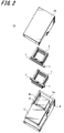
- FIG. 2 is an exploded perspective view of the variable inductor 10.
- illustration of the support members for the external electrode 6 and the movable core 5 is omitted.
- the first coil 1 is fitted and installed in the magnetic core core portion 4a provided in the magnetic core 3a, and the second magnetic core core portion 4b (see FIG. 1) provided in the magnetic core 3b is second. It is shown that the coil 2 is installed.
- the movable core 5 is shown to be movable along the guide groove 8.
- FIG. 3 shows an example of a first coil connection method.
- the first coil 1 and the second coil 2 included in the variable inductor 10 are connected in parallel.
- the first coil 1 and the second coil 2 have the same winding method, and the winding axis of the first coil 1 and the winding axis of the second coil 2 coincide with each other (in this example, the air core
- the air core axis is arranged in the same direction.
- the arrows of the conductors indicate the direction of current, and the first coil 1 and the second coil 2 generate magnetic flux by the current input from the input unit 11 and output from the output unit 12.
- the magnetic fluxes generated by the first coil 1 and the second coil 2 have the same density but opposite directions. For this reason, the magnetic flux generated inside the first coil 1 and the second coil 2 is almost canceled out.
- the slight magnetic flux 9 leaks from between the first coil 1 and the second coil 2 to the outside, but is not strong enough to cause interference electromagnetic waves.
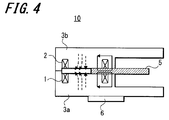
- FIG. 4 shows an example of a cross-sectional view along the line BB ′ of the variable inductor 10 in FIG. 1A.
- FIG. 4 shows an example in which the direction of magnetic flux generated in the variable inductor 10 is modeled will be described.
- the first coil 1 and the second coil 2 are accommodated in the magnetic cores 3 a and 3 b, and the movable core 5 is inserted between the first coil 1 and the second coil 2.
- the movable core 5 moves in a direction perpendicular to the winding axis direction of the first coil 1 and the second coil 2.
- the movable core 5 and the magnetic cores 3a and 3b constitute a closed magnetic circuit.
- an inductance is generated in a portion where magnetic fluxes in opposite directions generated by the first coil 1 and the second coil 2 merge.
- the upper and lower magnetic fluxes are canceled out at the portion not blocked by the movable core 5 and do not contribute to the inductance. For this reason, it is possible to adjust the inductance value by changing the insertion degree of the movable core 5 and adjusting the amount of magnetic flux contributing to the inductance.
- variable inductor 10 Next, an example of a process for manufacturing the variable inductor 10 will be described with reference to FIG.
- FIG. 5 shows an example of a cross-sectional view of the magnetic cores 3a and 3b along the line B-B ′ of the variable inductor 10 in FIG. 1A.
- the magnetic cores 3a and 3b and the magnetic core core 4a are formed.
- the magnetic cores 3a and 3b and the magnetic core core 4a are formed by pressing a raw powder, for example, a soft magnetic ferrite powder such as Ni-Zn ferrite into a desired shape, and then baking and solidifying it as a sintered body in a firing furnace.
- a raw powder for example, a soft magnetic ferrite powder such as Ni-Zn ferrite
- the magnetic cores 3a and 3b that are vertically symmetrical are formed.
- the air-core first coil 1 and second coil 2 are formed.
- the first coil 1 and the second coil 2 are mounted on the magnetic cores 3a and 3b, respectively, and then the plate-shaped movable core 5 and an actuator (not shown) are mounted.
- the coil end lead portion 7 is extended from the walls of the magnetic cores 3a and 3b.
- the magnetic cores 3a and 3b are combined and bonded and fixed with an adhesive or the like, and the external electrode 6 is formed outside the magnetic cores 3a and 3b.
- variable inductor 10 from the state in which a complete closed magnetic circuit is formed with a magnetic material, the open magnetic circuit state is further maintained, and the magnetic material is further away from the coil.
- the variable range of the inductance can be expanded.
- the magnetic fluxes emitted from the first coil 1 and the second coil 2 are in opposite directions, the magnetic fluxes can be canceled out.
- the first coil 1 and the second coil 2 are included in the magnetic cores 3a and 3b, and a closed magnetic circuit structure is formed through the magnetic cores 3a and 3b and the magnetic core core portion 4a. For this reason, there is an effect that leakage magnetic flux is hardly generated outside the variable inductor 10.
- the movable core 5 is opened and closed by an actuator (not shown) so as to be inserted or separated between the first coil 1 and the second coil 2.
- an actuator not shown
- inductance is generated by magnetic fluxes that do not cancel each other out of the magnetic fluxes generated by the first coil 1 and the second coil 2.
- the variable range of the inductance of the variable inductor 10 is wider than that of a general variable inductor.
- the inductance can be easily adjusted by the movable core 5 blocking the magnetic flux generated by the first coil 1 and the second coil 2.
- an adjustment unit for adjusting the position of the movable core 5 with respect to the first coil 1 and the second coil 2 is provided in one or both of the magnetic cores 3a and 3b. May be.
- the movable core 5 can move with a slight force along the guide groove 8 by the actuator. For this reason, the inductance can be finely adjusted to a desired value.
- variable inductor 10 is not limited to the process described in the first embodiment. Various manufacturing processes, manufacturing orders, and modifications are possible without departing from the gist of the present invention.
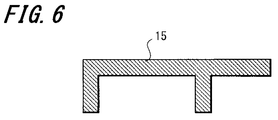
- FIG. 6 shows a modification of the magnetic cores 3a and 3b.
- the magnetic core 15 whose cross-sectional shape is shown in FIG. You can put it inside.
- a step of adhering them with a resin or the like may be added. Further, after the first coil 1 and the second coil 2 are put in the magnetic cores 3a and 3b, a mixture of resin and ferrite powder may be put and sintered so as to cover the coils. Further, a support member for supporting the movable core 5 may be placed in the gap between the magnetic cores 3a and 3b and the movable core 5, or a filler such as resin may be added.
- the magnetic cores 3a and 3b are not limited to a hexahedron, but may be a cylinder or a polyhedron.
- FIGS. Also in the present embodiment, for example, an example applied to a variable inductor 20 employed in a small electronic device or electronic circuit will be described.
- parts corresponding to those in FIG. 1 already described in the first embodiment are denoted by the same reference numerals, and detailed description thereof is omitted.
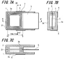
- FIG. 7A, 7B, and 7C show configuration examples of the variable inductor 20.
- FIG. FIG. 7A shows a configuration example of the variable inductor 20 in a top view.
- FIG. 7B shows an example of a cross-sectional view along the line AA ′ of the variable inductor 20 in FIG. 7A.
- FIG. 7C shows an example of a cross-sectional view along the line BB ′ of the variable inductor 20 in FIG. 7A.
- variable inductor 20 The configuration of the variable inductor 20 is substantially the same as the configuration of the variable inductor 10 according to the first embodiment described above. However, the variable inductor 20 is different in that the first coil 1 and the second coil 2 are connected in series and the magnetic core core portions 4a and 4b are not provided. For this reason, the magnetic core having a closed magnetic circuit structure including the first coil 1, the second coil 2 and the movable core 5 includes the first magnetic core 3 a including the first coil 1 and the second coil 2. It is only formed by combining the second magnetic core 3b provided. In order to generate magnetic fluxes from the first coil 1 and the second coil 2 in opposite directions, the winding directions of the two conductors are the same.
- the variable inductor 20 is provided with a connection electrode 21 to which the first coil 1 and the second coil 2 are connected in series. Since the connection electrode 21 is installed on the side surfaces of the magnetic cores 3 a and 3 b, notches are formed on the side surfaces of the magnetic cores 3 a and 3 b corresponding to the connection electrode 21.
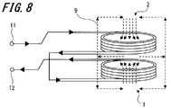
- FIG. 8 shows an example of a second coil connection method.
- the first coil 1 and the second coil 2 included in the variable inductor 20 are connected in series.
- the first coil 1 and the second coil 2 have the same winding method, and the axis of the air core is arranged in the same direction.
- the first coil 1 and the second coil 2 generate magnetic flux by the current input from the input unit 11 and output from the output unit 12.
- the magnetic fluxes generated by the first coil 1 and the second coil 2 have the same density and the same direction.
- the variable inductor 20 has an example in which the magnetic core cores 4a and 4b are not provided, but this is for improving the superposition characteristics of the variable inductor.
- a magnetic flux density passing through a magnetic core wound around the coil increases, and a phenomenon called “magnetic saturation” occurs. Due to this phenomenon, there arises a problem that the inductance is lowered even though the current is increased.
- DC superposition characteristics that represents the relationship between current and inductance value.
- the magnetic core core portions 4a and 4b are eliminated so as not to cause magnetic saturation.
- a comparative example of the variable range of the inductance values of the variable inductors 10 and 20 will be described with reference to FIGS.
- a comparative sample was prepared using the conventional technique, and the variable range of the inductance values of the comparative sample and the variable inductors 10 and 20 was compared.
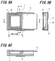
- FIG. 9A, 9B and 9C show configuration examples of comparative samples.
- FIG. 9A shows a configuration example of a comparative sample when viewed from above.
- FIG. 9B shows an example of a cross-sectional view along the line AA ′ of the comparative sample in FIG. 9A.
- FIG. 9C shows an example of a cross-sectional view along the line BB ′ of the comparative sample in FIG. 9A.
- the structure of the comparative sample is almost the same as that of the variable inductor 20. However, the comparative sample is in a state in which the second coil 2 and the upper magnetic core 3b are removed. For this reason, a comparative sample becomes an open magnetic circuit structure.
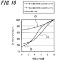
- FIG. 10 shows an example of the rate of change of the inductance value between the variable inductors 10 and 20 and the comparative sample when the position of the movable core 5 is changed.
- the broken line 23 indicating the inductance ratio of the variable inductor 10 the broken line 24 indicating the inductance ratio of the variable inductor 20, and the bent line 25 indicating the inductance ratio of the comparative sample represent the inductance ratio with respect to the position of the movable core 5.
- the position when the movable core 5 completely shuts off the first coil 1 and the second coil 2 is “10”, and the movable core 5 is completely removed from the first coil 1 and the second coil 2.
- the position is set to “0” (see FIGS. 1A, 7A, and 9A).
- the relative position of the movable core 5 with respect to the position “0” is referred to as “movable core position”.
- the inductance value when the movable core 5 is at the position “10” is set to “1”, and is normalized with respect to the inductance values at other positions.
- the inductance ratios of the variable inductors 10 and 20 at the movable core position “0” are both around 20%, whereas the inductance ratio of the comparative sample is around 70%. For this reason, it can be said that the change ratio of the inductance ratio of the variable inductors 10 and 20 is larger than that of the comparative sample.
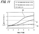
- FIG. 11 shows an example of a specific relationship between the inductance value and the position.
- FIG. 11 shows an example of inductance values of the variable inductors 10 and 20 and the comparative sample when the position of the movable core 5 is changed.
- the broken line 26 indicating the inductance value of the variable inductor 10
- the broken line 27 indicating the inductance value of the variable inductor 20
- the bent line 28 indicating the inductance value of the comparative sample represent the inductance value with respect to the position of the movable core 5.
- the inductance value of the variable inductor 10 when the movable core position is “10” is about 3.3 ⁇ H
- the inductance value of the variable inductor 20 is about 2.2 ⁇ H.
- the inductance value of the comparative sample is about 1.0 ⁇ H. For this reason, it can be said that the change rate of the inductance values of the variable inductors 10 and 20 is larger than the inductance value of the comparative sample.
- the inductance values of the variable inductors 10 and 20 are such that when the movable core 5 is inserted and the first coil 1 and the second coil 2 are cut off, the first coil 1 and the second coil 2 are independent of each other. Since the magnetic path is formed, the interaction of the generated magnetic flux becomes extremely small. On the other hand, since the first coil 1 and the second coil 2 function as two independent inductors, an inductance value is obtained when the two inductors are connected in series or in parallel. On the other hand, in a state in which the movable core 5 is removed from the first coil 1 and the second coil 2, the first coil 1 and the second coil 2 cancel each other out of the magnetic flux, so that a gap occurs between the two coils. Inductance is generated only by leakage flux. For this reason, inductance becomes a very small value. At this time, since the generated magnetic flux is suppressed as compared with the case where one coil has an open magnetic circuit structure, the inductance value becomes extremely small.
- variable inductors 10 and 20 have a wider inductance variable range than the comparative sample.
- the first coil 1 and the second coil 2 are manufactured using the same material, the same number of turns, and the same winding method. The number may not be the same winding method.
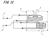
- FIG. 12 shows the state of magnetic flux when the winding axes and end face areas of the first coil 1 and the second coil 2 are different. It is assumed that the first coil 1 and the second coil 2 are connected in series (second connection method of the coil). In this case, in the variable inductor 20, for example, the winding axes of the first coil 1 and the second coil 2 do not completely coincide with each other, or the end surface areas of the first coil 1 and the second coil 2 are different. ing. However, if the first coil 1 and the second coil 2 cancel each other and reduce the magnetic flux, the operation and effect according to the present invention can be obtained. Further, even with the variable inductor 20 having such a configuration, an effect that the change width of the inductance becomes larger than that of the comparative sample can be obtained.
- variable inductor 10 when the first coil 1 and the second coil 2 are connected in parallel (the first connection method of the coil), the winding axes of the first coil 1 and the second coil 2. As described above, the functions and effects of the present invention can be obtained even if the first coil 1 and the second coil 2 have different end surface areas.
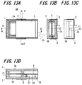
- FIG. 13A, B, C, and D show a configuration example of the variable inductor 30.
- FIG. FIG. 13A shows a configuration example of the variable inductor 30 when viewed from above.
- FIG. 13B shows an example of a cross-sectional view along the line AA ′ of the variable inductor 30 in FIG. 13A.
- FIG. 13C shows a configuration example when the variable inductor 30 in FIG. 13A is viewed from the direction of the arrow 35.
- FIG. 13D shows an example of a cross-sectional view along the line BB ′ of the variable inductor 30 in FIG. 13A.
- variable inductor 30 is substantially the same as that of the variable inductor 20 according to the second embodiment described above. However, the variable inductor 30 is different in that it includes a screw-type adjusting means for moving the movable core 5.
- an adjustment screw 31 that can adjust the position of the movable core 5 is disposed in the magnetic core 3 a in the gap between the upper and lower cores outside the variable inductor 30.
- a first thread groove is formed in the adjustment screw 31.
- a thread groove 32 is formed on the surface of the movable core 5 in contact with the adjustment screw 31 as a second thread groove that is preliminarily matched with the first thread groove.
- a screw stopper 34 is disposed at one end of the adjustment screw 31 so that the adjustment screw 31 does not fall off the variable inductor 30.
- a screw guide 33 is formed around the adjusting screw 31 with a material such as resin.
- the adjusting means for adjusting the position of the movable core 5 is not limited to a screw type, and for example, means such as a motor can be used.
- the first coil 1 and the second coil 2 may be connected in either a serial or parallel manner.
- the first coil 1 and the second coil 2 are preferably formed of the same material, the same number of turns, and the same winding method, but at least one of the winding shaft or the end surface area is different. May be.
- the magnetic fluxes generated by the first coil 1 and the second coil 2 are slightly different. However, if the magnetic fluxes are generated in a direction that cancels out the mutual magnetic fluxes as much as possible, they function as a variable inductor, so that the desired effect is obtained. Can be obtained.
Landscapes
- Engineering & Computer Science (AREA)
- Power Engineering (AREA)
- Coils Or Transformers For Communication (AREA)
Abstract
Description
図1Aは、上面視した場合における可変インダクタ10の構成例を示す。
図1Bは、図1Aにおける可変インダクタ10のA-A’線に沿った断面図の例を示す。
図1Cは、図1Aにおける可変インダクタ10のB-B’線に沿った断面図の例を示す。
図2において、外部電極6や可動コア5の支持部材については図示を省略する。図2より、磁性コア3aに設けられた磁性コア中芯部4aに第1のコイル1がはめ込んで設置され、磁性コア3bに設けられた磁性コア中芯部4b(図1参照)に第2のコイル2がはめ込んで設置されることが示される。また、可動コア5は、ガイド溝8に沿って、移動可能であることが示される。
可変インダクタ10が備える第1のコイル1と第2のコイル2は、並列接続される。第1のコイル1と第2のコイル2は、巻線方式が同じであり、第1のコイル1の巻線軸及び第2のコイル2の巻線軸が互いに一致する箇所(本例では、空芯の軸)であって、この空芯の軸が同じ方向に配置される。導線の矢印は電流の方向を示しており、入力部11から入力され、出力部12から出力される電流により、第1のコイル1と第2のコイル2が磁束を発生する。ここで、第1のコイル1と第2のコイル2が発する磁束は、密度が同じであるが、方向は反対となる。このため、第1のコイル1と第2のコイル2の内部に生じる磁束はほとんど打ち消される。ただし、わずかな漏れ磁束9は、第1のコイル1と第2のコイル2の間から外部へ漏れ出すが、妨害電磁波の要因となるほど強い磁束ではない。
ここでは、可変インダクタ10に生じる磁束の向きをモデル化した例について説明する。
次に、コイル端部引出部7を磁性コア3a,3bの壁から延出する。
最後に、磁性コア3a,3bを合わせて接着剤等により接着固定し、磁性コア3a,3bの外部に外部電極6を形成する。
上述した第1の実施の形態に係る磁性コア3a,3bの代わりに、断面形状が図6に示されるような磁性コア15を焼結し、I型コアに巻線されたコイルを磁性コア15の内部に入れても良い。
本実施の形態においても、例えば、小型の電子機器、電子回路に採用される可変インダクタ20に適用した例について説明する。以下の説明において、既に第1の実施の形態で説明した図1に対応する部分には同一符号を付し、詳細な説明を省略する。
図7Aは、上面視した場合における可変インダクタ20の構成例を示す。
図7Bは、図7Aにおける可変インダクタ20のA-A’線に沿った断面図の例を示す。
図7Cは、図7Aにおける可変インダクタ20のB-B’線に沿った断面図の例を示す。
第1のコイル1と第2のコイル2からの磁束を向かい合う方向に発生させるために、両者の導線の巻方向は同一とする。そして、可変インダクタ20には、第1のコイル1と第2のコイル2が直列接続される接続電極21が設置される。接続電極21は、磁性コア3a,3bの側面に設置されるため、接続電極21に対応する磁性コア3a,3bの側面に切欠部が形成される。
可変インダクタ20が備える第1のコイル1と第2のコイル2は、直列接続される。第1のコイル1と第2のコイル2は、巻線方式が同じであり、空芯の軸が同じ方向に配置される。入力部11から入力し、出力部12から出力する電流により、第1のコイル1と第2のコイル2が磁束を発生する。第1のコイル1と第2のコイル2が発する磁束は、密度が同じであり、方向は同じとなる。
図9Aは、上面視した場合における比較サンプルの構成例を示す。
図9Bは、図9Aにおける比較サンプルのA-A’線に沿った断面図の例を示す。
図9Cは、図9Aにおける比較サンプルのB-B’線に沿った断面図の例を示す。
図11は、可動コア5の位置を変えた場合における、可変インダクタ10,20と比較サンプルとのインダクタンス値の例を表している。図11において、可変インダクタ10のインダクタンス値を示す折れ線26,可変インダクタ20のインダクタンス値を示す折れ線27及び比較サンプルのインダクタンス値を示す折れ線28によって、可動コア5の位置に対するインダクタンス値を表している。
この場合、可変インダクタ20は、例えば、第1のコイル1と第2のコイル2の巻線軸が完全に一致しておらず、又は第1のコイル1と第2のコイル2の端面面積が異なっている。しかし、第1のコイル1と第2のコイル2が互いに磁束を打ち消し、減少する構成であれば、本発明に係る作用及び効果を得ることができる。また、このような構成とした可変インダクタ20であっても、比較サンプルに対してインダクタンスの変化幅が大きくなるという効果が得られる。
本実施の形態においても、例えば、小型の電子機器、電子回路に採用される可変インダクタ30に適用した例について説明する。以下の説明において、既に第1の実施の形態で説明した図1に対応する部分には同一符号を付し、詳細な説明を省略する。
図13Aは、上面視した場合における可変インダクタ30の構成例を示す。
図13Bは、図13Aにおける可変インダクタ30のA-A’線に沿った断面図の例を示す。
図13Cは、図13Aにおける可変インダクタ30を矢印35方向から視認した場合における構成例を示す。
図13Dは、図13Aにおける可変インダクタ30のB-B’線に沿った断面図の例を示す。
Claims (11)
- 第1のコイルと、
上記第1のコイルが発する磁束を打ち消す方向に磁束を発する第2のコイルと、
上記第1のコイル及び上記第2のコイルの間に移動することによって、上記第1のコイル及び上記第2のコイルが発する磁束を遮る可動コアと、
上記第1のコイル、上記第2のコイル及び上記可動コアを内包する閉磁路構造の磁性コアと、を備える
可変インダクタ。 - 上記磁性コアは、上記第1のコイルを備える第1の磁性コアと、上記第2のコイルを備える第2の磁性コアを組み合わせて形成され、
上記第1の磁性コアは、上記第1のコイルが巻回される第1の中芯部を備え、
上記第2の磁性コアは、上記第2のコイルが巻回される第2の中芯部を備える
請求の範囲第1項記載の可変インダクタ。 - 上記磁性コアは、上記第1のコイルを備える第1の磁性コアと、上記第2のコイルを備える第2の磁性コアを組み合わせて形成される
請求の範囲第1項記載の可変インダクタ。 - 上記磁性コアには、上記可動コアの移動方向に溝が形成され、
上記可動コアは、平板状に形成され、上記溝に沿って移動可能とされる
請求の範囲第2項又は第3項記載の可変インダクタ。 - 上記第1のコイルの巻線軸及び上記第2のコイルの巻線軸が互いに一致する箇所に、上記第1及び第2のコイルが配置され、
上記可動コアは、上記第1及び第2のコイルの巻線軸方向に対して垂直方向に移動する
請求の範囲第4項記載の可変インダクタ。 - さらに、上記可動コアの上記第1及び第2のコイルに対する位置を調整する調整部を備える
請求の範囲第1項~第5項のいずれか1項に記載の可変インダクタ。 - 上記磁性コアに配置される上記調整部には、第1のねじ溝が形成され、
上記可動コアの上記第1のねじ溝が接する面には、上記第1のねじ溝に合わせた第2のねじ溝が形成される
請求の範囲第6項記載の可変インダクタ。 - 上記第1のコイルと上記第2のコイルが直列に接続される
請求の範囲第1項~第7項のいずれか1項に記載の可変インダクタ。 - 上記第1のコイルと上記第2のコイルが並列に接続される
請求の範囲第1項~第7項のいずれか1項に記載の可変インダクタ。 - 上記第1及び第2のコイルは、上記巻線軸又は端面面積のうち、少なくともいずれかが異なる
請求の範囲第8項又は第9項記載の可変インダクタ。 - 上記第1及び第2のコイルは、同じ材料、同じターン数、及び同じ巻線方法で形成される
請求の範囲第8項又は第9項記載の可変インダクタ。
Priority Applications (3)
| Application Number | Priority Date | Filing Date | Title |
|---|---|---|---|
| CN2009801414853A CN102187410B (zh) | 2008-12-08 | 2009-09-07 | 可变电感 |
| KR1020117005355A KR101219568B1 (ko) | 2008-12-08 | 2009-09-07 | 가변 인덕터 |
| US13/154,099 US8319592B2 (en) | 2008-12-08 | 2011-06-06 | Variable inductor |
Applications Claiming Priority (2)
| Application Number | Priority Date | Filing Date | Title |
|---|---|---|---|
| JP2008-312547 | 2008-12-08 | ||
| JP2008312547A JP5127060B2 (ja) | 2008-12-08 | 2008-12-08 | 可変インダクタ |
Related Child Applications (1)
| Application Number | Title | Priority Date | Filing Date |
|---|---|---|---|
| US13/154,099 Continuation US8319592B2 (en) | 2008-12-08 | 2011-06-06 | Variable inductor |
Publications (1)
| Publication Number | Publication Date |
|---|---|
| WO2010067649A1 true WO2010067649A1 (ja) | 2010-06-17 |
Family
ID=42242642
Family Applications (1)
| Application Number | Title | Priority Date | Filing Date |
|---|---|---|---|
| PCT/JP2009/065563 Ceased WO2010067649A1 (ja) | 2008-12-08 | 2009-09-07 | 可変インダクタ |
Country Status (5)
| Country | Link |
|---|---|
| US (1) | US8319592B2 (ja) |
| JP (1) | JP5127060B2 (ja) |
| KR (1) | KR101219568B1 (ja) |
| CN (1) | CN102187410B (ja) |
| WO (1) | WO2010067649A1 (ja) |
Cited By (2)
| Publication number | Priority date | Publication date | Assignee | Title |
|---|---|---|---|---|
| US20120293170A1 (en) * | 2009-12-28 | 2012-11-22 | Hiroyoshi Nakajima | Magnetic field detection device and current sensor |
| JPWO2018012354A1 (ja) * | 2016-07-13 | 2019-04-25 | 新日鐵住金株式会社 | インダクタンス調整装置 |
Families Citing this family (7)
| Publication number | Priority date | Publication date | Assignee | Title |
|---|---|---|---|---|
| KR101223607B1 (ko) * | 2011-10-31 | 2013-01-21 | 경북대학교 산학협력단 | 가변 인덕터 및 그 인덕터의 구동 방법 |
| JP6245187B2 (ja) * | 2015-02-02 | 2017-12-13 | 株式会社村田製作所 | パワーインダクタの評価装置、及び、パワーインダクタの評価プログラム |
| JP6447405B2 (ja) | 2015-08-04 | 2019-01-09 | 株式会社村田製作所 | 可変インダクタ |
| KR101893766B1 (ko) * | 2016-07-29 | 2018-08-31 | 신찬수 | 가변 리액터 |
| EP3422417B1 (en) | 2017-06-30 | 2021-08-04 | Murata Manufacturing Co., Ltd. | Distributed lc filter structure |
| US11049642B1 (en) * | 2017-09-26 | 2021-06-29 | Universal Lighting Technologies, Inc. | Dual magnetic component with three core portions |
| FR3142851B1 (fr) * | 2022-12-06 | 2025-01-03 | Thales Sa | Module de variation d'une inductance et filtre radiofréquence comportant un tel module |
Citations (3)
| Publication number | Priority date | Publication date | Assignee | Title |
|---|---|---|---|---|
| JPS48105016U (ja) * | 1972-03-10 | 1973-12-07 | ||
| JPS6367710A (ja) * | 1986-09-09 | 1988-03-26 | Fujitsu Ltd | 小型可変インダクタ |
| JP2005064263A (ja) * | 2003-08-13 | 2005-03-10 | Rikogaku Shinkokai | 可変インダクタ |
Family Cites Families (14)
| Publication number | Priority date | Publication date | Assignee | Title |
|---|---|---|---|---|
| GB1188326A (en) * | 1967-08-21 | 1970-04-15 | Hirst Electric Ind Ltd | Transformer with Variable Secondary Reactance |
| US3716719A (en) * | 1971-06-07 | 1973-02-13 | Aerco Corp | Modulated output transformers |
| US4031496A (en) * | 1973-07-06 | 1977-06-21 | Hitachi, Ltd. | Variable inductor |
| US4149133A (en) * | 1977-10-14 | 1979-04-10 | Johnson Controls, Inc. | Variable differential transformer apparatus |
| JPS5932049B2 (ja) * | 1979-10-22 | 1984-08-06 | 東北金属工業株式会社 | ノイズフィルタ用インダクタ |
| JPS59178713A (ja) * | 1983-03-29 | 1984-10-11 | Mitsubishi Electric Corp | 可変リアクトル |
| US5061896A (en) * | 1985-09-03 | 1991-10-29 | United Technologies Corporation | Variable transformer to detect linear displacement with constant output amplitude |
| JPS62111405A (ja) * | 1985-11-08 | 1987-05-22 | Matsushita Electric Ind Co Ltd | 可変インダクタ |
| US4837497A (en) * | 1987-12-29 | 1989-06-06 | Gregory Leibovich | Variable transformer, reactor and method of their control |
| JPH03166706A (ja) * | 1989-11-27 | 1991-07-18 | Shimada Phys & Chem Ind Co Ltd | 可変インダクタ |
| JPH03217004A (ja) * | 1990-01-22 | 1991-09-24 | Nec Corp | 可変インダクタ |
| US6681728B2 (en) * | 2001-11-05 | 2004-01-27 | Ford Global Technologies, Llc | Method for controlling an electromechanical actuator for a fuel air charge valve |
| JP2005064308A (ja) | 2003-08-18 | 2005-03-10 | Rikogaku Shinkokai | 可変インダクタ |
| JP2006286805A (ja) | 2005-03-31 | 2006-10-19 | Fujitsu Ltd | 可変インダクタ |
-
2008
- 2008-12-08 JP JP2008312547A patent/JP5127060B2/ja not_active Expired - Fee Related
-
2009
- 2009-09-07 CN CN2009801414853A patent/CN102187410B/zh not_active Expired - Fee Related
- 2009-09-07 WO PCT/JP2009/065563 patent/WO2010067649A1/ja not_active Ceased
- 2009-09-07 KR KR1020117005355A patent/KR101219568B1/ko not_active Expired - Fee Related
-
2011
- 2011-06-06 US US13/154,099 patent/US8319592B2/en not_active Expired - Fee Related
Patent Citations (3)
| Publication number | Priority date | Publication date | Assignee | Title |
|---|---|---|---|---|
| JPS48105016U (ja) * | 1972-03-10 | 1973-12-07 | ||
| JPS6367710A (ja) * | 1986-09-09 | 1988-03-26 | Fujitsu Ltd | 小型可変インダクタ |
| JP2005064263A (ja) * | 2003-08-13 | 2005-03-10 | Rikogaku Shinkokai | 可変インダクタ |
Cited By (3)
| Publication number | Priority date | Publication date | Assignee | Title |
|---|---|---|---|---|
| US20120293170A1 (en) * | 2009-12-28 | 2012-11-22 | Hiroyoshi Nakajima | Magnetic field detection device and current sensor |
| US9086444B2 (en) * | 2009-12-28 | 2015-07-21 | Tdk Corporation | Magnetic field detection device and current sensor |
| JPWO2018012354A1 (ja) * | 2016-07-13 | 2019-04-25 | 新日鐵住金株式会社 | インダクタンス調整装置 |
Also Published As
| Publication number | Publication date |
|---|---|
| KR20110039388A (ko) | 2011-04-15 |
| US8319592B2 (en) | 2012-11-27 |
| CN102187410B (zh) | 2013-04-17 |
| JP2010135699A (ja) | 2010-06-17 |
| CN102187410A (zh) | 2011-09-14 |
| KR101219568B1 (ko) | 2013-01-09 |
| US20110234354A1 (en) | 2011-09-29 |
| JP5127060B2 (ja) | 2013-01-23 |
Similar Documents
| Publication | Publication Date | Title |
|---|---|---|
| JP5127060B2 (ja) | 可変インダクタ | |
| US20240234005A1 (en) | Packaging Structure of a Magnetic Device | |
| JP6331060B2 (ja) | 面実装型リアクトル及びその製造方法 | |
| US5841335A (en) | Choke coil | |
| US11398338B2 (en) | Reactor | |
| JP2009016797A (ja) | インダクター | |
| JPWO2009066433A1 (ja) | コイル部品 | |
| JPWO1995029493A1 (ja) | チョークコイル | |
| JP3818465B2 (ja) | インダクタンス素子 | |
| JP6558128B2 (ja) | コイル装置 | |
| US7345566B2 (en) | Magnetic element | |
| JP2004103624A (ja) | トランス及びその製造方法 | |
| US20110080243A1 (en) | Inductor | |
| JP6781043B2 (ja) | 複合磁路インダクタ | |
| US20110121929A1 (en) | Inductor Structure | |
| JP2005353989A (ja) | 複合型インダクタ | |
| KR101234875B1 (ko) | Pfc 미적용 전원부의 emi 필터 및 이를 포함하는 평판 디스플레이 장치 | |
| JP2021022724A (ja) | インダクタ | |
| JP2018006460A (ja) | ラインフィルタ | |
| KR20180115869A (ko) | Smps의 누설자속을 배제하는 코어 갭 구조 | |
| JP2022013716A (ja) | 磁気シェル及び磁気装置 | |
| KR101730792B1 (ko) | 샌드위치형 자성시트 | |
| JP2008016468A (ja) | トランス | |
| JP6376317B1 (ja) | アンテナ装置および電子機器 | |
| WO2025009205A1 (ja) | 磁性部品および電気・電子機器 |
Legal Events
| Date | Code | Title | Description |
|---|---|---|---|
| WWE | Wipo information: entry into national phase |
Ref document number: 200980141485.3 Country of ref document: CN |
|
| 121 | Ep: the epo has been informed by wipo that ep was designated in this application |
Ref document number: 09831755 Country of ref document: EP Kind code of ref document: A1 |
|
| ENP | Entry into the national phase |
Ref document number: 20117005355 Country of ref document: KR Kind code of ref document: A |
|
| NENP | Non-entry into the national phase |
Ref country code: DE |
|
| 122 | Ep: pct application non-entry in european phase |
Ref document number: 09831755 Country of ref document: EP Kind code of ref document: A1 |