WO2010067485A1 - シールドフィルム及びシールド配線板 - Google Patents
シールドフィルム及びシールド配線板 Download PDFInfo
- Publication number
- WO2010067485A1 WO2010067485A1 PCT/JP2009/003677 JP2009003677W WO2010067485A1 WO 2010067485 A1 WO2010067485 A1 WO 2010067485A1 JP 2009003677 W JP2009003677 W JP 2009003677W WO 2010067485 A1 WO2010067485 A1 WO 2010067485A1
- Authority
- WO
- WIPO (PCT)
- Prior art keywords
- siloxane
- shield film
- adhesive layer
- conductive adhesive
- polyimide
- Prior art date
- Legal status (The legal status is an assumption and is not a legal conclusion. Google has not performed a legal analysis and makes no representation as to the accuracy of the status listed.)
- Ceased
Links
Images


Classifications
-
- H—ELECTRICITY
- H05—ELECTRIC TECHNIQUES NOT OTHERWISE PROVIDED FOR
- H05K—PRINTED CIRCUITS; CASINGS OR CONSTRUCTIONAL DETAILS OF ELECTRIC APPARATUS; MANUFACTURE OF ASSEMBLAGES OF ELECTRICAL COMPONENTS
- H05K9/00—Screening of apparatus or components against electric or magnetic fields
- H05K9/0073—Shielding materials
- H05K9/0081—Electromagnetic shielding materials, e.g. EMI, RFI shielding
- H05K9/0083—Electromagnetic shielding materials, e.g. EMI, RFI shielding comprising electro-conductive non-fibrous particles embedded in an electrically insulating supporting structure, e.g. powder, flakes, whiskers
-
- C—CHEMISTRY; METALLURGY
- C08—ORGANIC MACROMOLECULAR COMPOUNDS; THEIR PREPARATION OR CHEMICAL WORKING-UP; COMPOSITIONS BASED THEREON
- C08G—MACROMOLECULAR COMPOUNDS OBTAINED OTHERWISE THAN BY REACTIONS ONLY INVOLVING UNSATURATED CARBON-TO-CARBON BONDS
- C08G73/00—Macromolecular compounds obtained by reactions forming a linkage containing nitrogen with or without oxygen or carbon in the main chain of the macromolecule, not provided for in groups C08G12/00 - C08G71/00
- C08G73/06—Polycondensates having nitrogen-containing heterocyclic rings in the main chain of the macromolecule
- C08G73/10—Polyimides; Polyester-imides; Polyamide-imides; Polyamide acids or similar polyimide precursors
- C08G73/1057—Polyimides containing other atoms than carbon, hydrogen, nitrogen or oxygen in the main chain
- C08G73/106—Polyimides containing other atoms than carbon, hydrogen, nitrogen or oxygen in the main chain containing silicon
-
- C—CHEMISTRY; METALLURGY
- C08—ORGANIC MACROMOLECULAR COMPOUNDS; THEIR PREPARATION OR CHEMICAL WORKING-UP; COMPOSITIONS BASED THEREON
- C08G—MACROMOLECULAR COMPOUNDS OBTAINED OTHERWISE THAN BY REACTIONS ONLY INVOLVING UNSATURATED CARBON-TO-CARBON BONDS
- C08G73/00—Macromolecular compounds obtained by reactions forming a linkage containing nitrogen with or without oxygen or carbon in the main chain of the macromolecule, not provided for in groups C08G12/00 - C08G71/00
- C08G73/06—Polycondensates having nitrogen-containing heterocyclic rings in the main chain of the macromolecule
- C08G73/10—Polyimides; Polyester-imides; Polyamide-imides; Polyamide acids or similar polyimide precursors
- C08G73/1057—Polyimides containing other atoms than carbon, hydrogen, nitrogen or oxygen in the main chain
- C08G73/1064—Polyimides containing other atoms than carbon, hydrogen, nitrogen or oxygen in the main chain containing sulfur
-
- C—CHEMISTRY; METALLURGY
- C09—DYES; PAINTS; POLISHES; NATURAL RESINS; ADHESIVES; COMPOSITIONS NOT OTHERWISE PROVIDED FOR; APPLICATIONS OF MATERIALS NOT OTHERWISE PROVIDED FOR
- C09D—COATING COMPOSITIONS, e.g. PAINTS, VARNISHES OR LACQUERS; FILLING PASTES; CHEMICAL PAINT OR INK REMOVERS; INKS; CORRECTING FLUIDS; WOODSTAINS; PASTES OR SOLIDS FOR COLOURING OR PRINTING; USE OF MATERIALS THEREFOR
- C09D179/00—Coating compositions based on macromolecular compounds obtained by reactions forming in the main chain of the macromolecule a linkage containing nitrogen, with or without oxygen, or carbon only, not provided for in groups C09D161/00 - C09D177/00
- C09D179/04—Polycondensates having nitrogen-containing heterocyclic rings in the main chain; Polyhydrazides; Polyamide acids or similar polyimide precursors
- C09D179/08—Polyimides; Polyester-imides; Polyamide-imides; Polyamide acids or similar polyimide precursors
Definitions
- the present invention relates to a shield film excellent in electromagnetic wave shielding properties and a shield wiring board having the shield film attached thereto.
- circuit electromagnetic wave shielding films are stuck on the circuit forming surfaces of various wiring boards in the devices.
- an overcoat layer is provided on the circuit forming surface of the wiring board, and a ground opening for conducting the ground circuit and the shield film is formed in the overcoat layer.
- Patent Document 1 a film in which a shield layer is laminated on an insulating layer located on the outermost surface after being attached to a wiring board has been proposed.
- stacked on the epoxy resin insulating layer, and 20 weight part of silver coat copper powder as an electroconductive filler in the silver vapor deposition layer are flame-retardant.
- the anisotropic conductive adhesive layer of the wiring board is laminated on the anisotropic conductive adhesive layer of the shield film on the circuit forming surface of the wiring board and hot-pressed.
- the electromagnetic wave shielding property of the shield film is realized by curing while pushing into the ground opening, thereby conducting the ground circuit and the silver deposited layer.
- the object of the present invention is to solve the above-mentioned problems of the prior art, and there is no possibility of precipitation of phosphorus during solder reflow, and the shielding film does not impair electromagnetic wave shielding even when the ground opening is small. Is to provide.
- the present inventors have a limit in the use of the anisotropic conductive adhesive layer in relation to the ground opening diameter, the conductive property in which the conductive filler is dispersed in the binder resin in the insulating protective layer.
- the above-mentioned object can be achieved by including a specific siloxane residue-containing polyimide, which is a kind of thermoplastic resin that is flexible and has excellent indentability, in the binder resin.
- the present invention is a shield film in which a conductive adhesive layer in which a conductive filler is dispersed in a binder resin is laminated on a protective layer, and the binder resin contains a siloxane residue-containing polyimide.
- a shield film is provided.
- this invention is a manufacturing method of the above-mentioned shield film, Comprising: The following processes: Applying a coating material for forming a protective layer to the first release substrate, and forming a protective layer by drying; Applying a conductive adhesive layer-forming coating material containing a binder resin containing a siloxane residue-containing polyimide and a conductive filler to the second release substrate, and forming a conductive adhesive layer by drying; There is provided a manufacturing method comprising a step of forming a shield film by bonding a protective layer and a conductive adhesive layer to each other.
- the present invention provides a shield wiring board characterized in that the above-mentioned shield film is laminated with a conductive adhesive layer so as to be electrically connected to the ground wiring on the wiring board on which the ground wiring is formed. provide.
- the shield film of the present invention does not use a phosphorus-containing epoxy resin for the binder resin of the conductive adhesive layer, there is no possibility that phosphorus will precipitate during solder reflow.
- a specific polyimide containing thermoplastic siloxane residue is used, even when the ground opening of the wiring board is small, it is easy to push into the ground opening, so the reliability of conduction between the ground circuit and the conductive adhesive layer And high electromagnetic shielding properties can be realized. Moreover, good flame retardancy can be achieved.
- FIG. 1 is a cross-sectional view of a shield film.
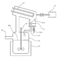
- FIG. 2 is an overall view of a synthesis apparatus for producing a siloxane polyimide resin.
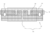
- FIG. 3 is a plan perspective view of the shield wiring board (the shield film is seen through).
- FIG. 4 is a measurement view of the shielding effect of the shielding film.
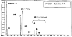
- FIG. 5 is a GC-MS chart of the vacuum recovery A obtained in Reference Example 1.
- FIG. 1 is a cross-sectional view of a shield film 10 of the present invention.
- This shield film 10 has a structure in which a conductive adhesive layer 4 in which a conductive filler 2 is dispersed in a binder resin 3 is laminated on a protective layer 1, and the binder resin 3 contains a siloxane residue-containing polyimide. It is characterized by that.
- the protective layer 1 constituting the shield film 10 of the present invention is located on the outer surface when the shield film is applied to an adherend such as a wiring board, and from the force or humidity from the outside of the adherend. It has a function to protect and also functions as a support for the conductive adhesive layer 4 described above.
- a protective layer 1 the same configuration as the protective layer in the conventional shield film 10 can be adopted.
- a resin film having a thickness of 5 to 15 ⁇ m for example, a polyester film, a polyimide film, a polyether film, a polyphenylene sulfide film, or the like can be used.
- a film in which a siloxane residue-containing polyimide constituting the binder resin of the conductive adhesive layer 4 described later is formed can be preferably used.
- the conductive adhesive layer 4 constituting the shield film 10 of the present invention is a layer that adheres the shield film 10 to an adherend such as a wiring board and exhibits electromagnetic shielding properties.
- the thickness of the conductive adhesive layer 4 is preferably 5 to 20 ⁇ m, more preferably 7 to 15 ⁇ m.
- the siloxane residue-containing polyimide constituting the binder resin 3
- the siloxane residue-containing polyimide is blended in the conductive adhesive layer, but this resin is thermoplastic, and when melted. It has a siloxane residue that contributes to improved fluidity. Moreover, it has an imide bond and a benzene ring that contribute to flame retardancy. Therefore, in the shield film of the present invention, there is no possibility that phosphorus is precipitated during solder reflow. Moreover, even when the ground opening of the wiring board is small, the conduction reliability between the ground circuit and the conductive adhesive layer can be improved, and good electromagnetic shielding properties can be realized. In addition, good flame retardancy can be achieved.
- preferred siloxane residue-containing polyimides include those having a repeating structural unit of the formula (A).
- n is an integer of 1 to 30, preferably 1 to 20, and m is an integer of 0 to 20, preferably 1 to 20.
- m is an integer of 0 to 20, preferably 1 to 20.
- m is an integer of 0 to 20, preferably 1 to 20.
- Specific examples of the siloxane residue-containing polyimide of the formula (A) include m-22, X-22-161A, X-22-161B, KF8008, KF8012 (above, Shin-Etsu Chemical Co., Ltd.), BY16-871, BY16.
- the siloxane residue of the siloxane residue-containing polyimide of the formula (A) is preferably derived from the siloxane diamine component when producing the polyimide, specifically derived from the siloxane diamine of the formula (1).
- n and m are as described in the formula (A).
- siloxane diamine those having an amino group protected by a carbamate type such as a tert-butoxycarbonyl group, an imide type such as a phthaloyl group, or a sulfonamide type such as a p-toluenesulfonyl group can be used.
- a carbamate type such as a tert-butoxycarbonyl group
- an imide type such as a phthaloyl group
- a sulfonamide type such as a p-toluenesulfonyl group
- the content of the siloxane residue-containing polyimide in the conductive adhesive layer 4 of the shield film 10 of the present invention is too small, it is difficult to push into the ground opening, and if it is too large, the content of the conductive filler is relatively reduced. In either case, the conduction reliability is lowered, so the content is preferably 4 to 12% by mass, more preferably 6 to 9% by mass.
- siloxane residue-containing polyimide used in the present invention one produced by a known method can be used, but at least tetracarboxylic dianhydride, siloxane diamine, What was obtained by the method of manufacturing siloxane polyimide resin by making this react can be used preferably. Specifically, those obtained by the production method having the following steps (a) to (c) can be preferably used.
- step (A) a step of imidizing a first tetracarboxylic dianhydride and a siloxane diamine in a solvent under a reflux condition to obtain a reaction mixture containing an acid anhydride terminal or an amine terminal siloxane imide oligomer;
- step (B) concentrating the reaction mixture obtained in step (a) under reduced pressure to obtain a reaction concentrate; and (c) adding a solvent and a siloxane-free diamine to the reaction concentrate obtained in step (b).
- siloxane-free diamine and the acid anhydride-terminated siloxane imide oligomer in the reaction concentrate are imidized, or the solvent and the second tetracarboxylic dianhydride are added, and the second tetracarboxylic acid is added.
- siloxane diamine out of diamine components is first subjected to an imidization reaction with a tetracarboxylic dianhydride component to obtain an acid anhydride terminal or amine terminal siloxane imide oligomer, and after the reaction is completed.
- the volatile impurities such as cyclic siloxane oligomer are removed together with the solvent under reduced pressure. For this reason, not only cyclic siloxane oligomers up to hexamers but also siloxane oligomers and free siloxane compounds of 7-mers or more that bleed out can be removed.
- Step (a) First, the first tetracarboxylic dianhydride and siloxane diamine are imidized under reflux conditions in a solvent to obtain a reaction mixture containing an acid anhydride terminal or amine terminal siloxane imide oligomer.
- the molar amount of the first tetracarboxylic dianhydride may be increased as compared with siloxane diamine.
- the molar amount of the first tetracarboxylic dianhydride may be made smaller than that of siloxane diamine.
- the amount of siloxane diamine used is too small relative to 1 mol of all tetracarboxylic dianhydrides, it tends to be difficult to maintain adhesion and flexibility, and if too large, heat resistance tends to decrease. Therefore, the amount is preferably 0.1 to 0.9 mol, more preferably 0.3 to 0.8 mol.
- the reason for carrying out the imidization reaction under reflux is to remove the imidized water by azeotropic distillation with a solvent using a Dean-Stark separation tube or the like. Therefore, as the solvent, a solvent that is refluxed at a temperature at which an imidization reaction between tetracarboxylic dianhydride and siloxane diamine occurs and can separate water by azeotropy is used.
- a solvent include glymes such as diglyme and triglyme, ether solvents such as dioxane and tetrahydrofuran, lactone solvents such as ⁇ -butyrolactone and ⁇ -valerolactone, and mixtures thereof.
- a nonpolar solvent such as toluene, xylene, benzene or mesitylene and a solvent such as N-methyl-2-pyrrolidone may be used in combination as long as the effects of the invention are not impaired.
- step (a) The amount of solvent used in step (a) varies depending on the type of solvent and reaction substrate, but if it is too small, it will cause poor monomer dispersion and decrease in reflux efficiency. If it is too large, the heat of vaporization of the solvent will increase and the temperature in the reaction vessel will increase. Therefore, the total mass of the first tetracarboxylic dianhydride and the siloxane diamine is preferably used in an amount of 5 to 60% by mass.
- the reaction temperature of the imidation reaction varies depending on the type and amount of the solvent and reaction substrate, but if it is too low, the imidization reaction cannot be completed, and if it is too high, side reactions other than the imidization reaction may occur.
- the temperature is preferably 150 to 220 ° C, more preferably 160 to 200 ° C.
- the reaction time is the time required to remove the theoretical amount of imidized water, and is usually 0.5 to 12 hours, preferably 1 to 8 hours.
- first tetracarboxylic dianhydride used in the present invention include pyromellitic dianhydride, 3,4,3 ', 4'-biphenyltetracarboxylic dianhydride, 4,4'- Oxydiphthalic dianhydride, 3,4,3 ', 4'-benzophenone tetracarboxylic dianhydride, 3,3', 4,4'-diphenylsulfone tetracarboxylic dianhydride, 9,9-bis (3 , 4-Dicarboxyphenyl) fluorene dianhydride, 9,9-bis [4- (3,4-dicarboxyphenoxy) phenyl] fluorene dianhydride, 2,3,6,7-naphthalenetetracarboxylic dianhydride 4,4 '-(hexafluoroisopropylidene) diphthalic anhydride, 1,2,3,4-cyclobutanetetracarboxylic dianhydride,
- the siloxane diamine used in the present invention is a compound having a dimethylsilylene skeleton at least in the molecule, and those conventionally used for siloxane modification of polyimide resins can be used. Especially, what has the structure of Formula (1) mentioned above from the point of a flame retardance and compatibility ensuring can be used preferably.
- a tertiary amine such as triethylamine
- a basic catalyst such as aromatic isoquinoline and pyridine
- an acid catalyst such as benzoic acid and parahydroxybenzoic acid
- Step (b) After completion of the reaction in step (a), the reaction mixture obtained in step (a) is concentrated under reduced pressure to obtain a reaction concentrate.
- This step (b) is a step of removing the cyclic siloxane oligomer when the cyclic siloxane oligomer is contained as an impurity in the siloxane diamine used in the step (a). That is, by concentrating under reduced pressure, a volatile cyclic siloxane oligomer and a free siloxane compound (for example, low molecular weight siloxane monoamine, low molecular weight siloxane) can be efficiently removed together with a solvent and a small amount of water.
- a volatile cyclic siloxane oligomer and a free siloxane compound for example, low molecular weight siloxane monoamine, low molecular weight siloxane
- the temperature during this concentration under reduced pressure is too low, the removal efficiency of the cyclic siloxane oligomer or free siloxane compound deteriorates, so the temperature is the same as the imidation reaction temperature in step (a) or the solvent boiling temperature at atmospheric pressure. It is preferable.
- the pressure at the time of concentration under reduced pressure is preferably 0.3 because the removal efficiency of the cyclic siloxane oligomer or free siloxane compound deteriorates if the degree of pressure reduction is not sufficient, and conversely, excessive pressure reduction causes an excessive increase in processing costs.
- ⁇ 91kPa more preferably 11 ⁇ 51kPa.
- Step (c) Next, when the reaction concentrate obtained in step (b) is an acid anhydride-terminated siloxane imide oligomer, a solvent and a siloxane-free diamine are added to the reaction concentrate, and a siloxane-free diamine and an acid are added.
- An anhydride-terminated siloxane imide oligomer is imidized to obtain a siloxane polyimide resin.
- reaction concentrate is an amine-terminated siloxane imide oligomer
- a solvent and a second tetracarboxylic dianhydride are added to the reaction concentrate, and the reaction concentration with the second tetracarboxylic dianhydride is added.
- the amine-terminated siloxane imide oligomer in the product is imidized to obtain a siloxane polyimide resin.
- a siloxane-free diamine may be added together with the second tetracarboxylic dianhydride as necessary.
- the solvent As the solvent, those that can be used in step (a) can be used. In particular, when a siloxane polyimide resin is used as a varnish, in order to prevent polyimide precipitation due to moisture absorption during coating, an ether solvent, a lactone solvent, a nonpolar solvent, etc., which are relatively low hygroscopic solvents, or Can be used as a mixture.
- a mixed solvent of triglyme also known as triethylene glycol dimethyl ether
- a diamine having no dimethylsilylene skeleton in the molecule can be used, and specific examples thereof include 3,3′-diamino-4,4 ′.
- -Dihydroxydiphenylsulfone 2,2-bis (3-amino-4-hydroxyphenyl) hexafluoropropane, 2,2-bis (3-amino-4-hydroxyphenyl) propane, 3,3'-diamino-4, Diaminophenol derivatives such as 4'-dihydroxydiphenylmethane, 3,3'-dihydroxy-4,4'-diaminobiphenyl, 2,4-diaminophenol, 9,9-bis (3-amino-4-hydroxyphenyl) fluorene; p-phenylenediamine, 4,4'-diaminodiphenyl ether, 2,2-bis [4- (4 Aminophenoxy) phenyl] propane, bis [4- (4- (4- (4 Aminophenoxy) phenyl] propane, bis
- the “second tetracarboxylic dianhydride” those similar to the first tetracarboxylic dianhydride already exemplified can be used.
- the first tetracarboxylic dianhydride and the second tetracarboxylic dianhydride may be the same or different.
- the amount of siloxane-free diamine used in step (c) is the molecular weight for obtaining a coverlay with sufficient mechanical properties.
- the total number of moles of siloxane diamine is preferably 0.1 to 0.9 mol, more preferably 0.3 to 0.8 mol, relative to 1 mol of all tetracarboxylic dianhydrides. This is the amount.
- the amount of the second tetracarboxylic dianhydride used in step (c) is sufficient in mechanical properties.
- siloxane diamine and siloxane are not contained with respect to 1 mole of the total number of moles of the first tetracarboxylic dianhydride and the second tetracarboxylic dianhydride.
- the total amount of diamine components combined with diamine is preferably 0.8 to 1.2 mol, more preferably 0.9 to 1.1 mol.
- a tertiary catalyst such as triethylamine, a basic catalyst such as aromatic isoquinoline, pyridine, benzoic acid, An acid catalyst such as parahydroxybenzoic acid may be added.
- step (c) When an acid dianhydride or diamine component having a polar group is used in step (c), the viscosity of the siloxane polyimide resin produced by the Weiselberg effect increases, and a phenomenon of winding around the stirring rod may occur. is there.
- water it is preferable that water be present in the reaction system. In this case, if the amount of water is too small, the risk of thickening increases, and if it is too large, the molecular weight of the polyimide may decrease. Therefore, water is added at a ratio of 0.01 to 1.1% by mass in the reaction mixture. Preferably it is present.
- the reaction temperature at the time of imidization in step (c) varies depending on the type and amount of the solvent and reaction substrate, but if it is too low, the imidization reaction is not completed, and if it is too high, side reactions other than the imidization reaction occur. Since there is a possibility, it is preferably 150 to 220 ° C., more preferably 160 to 200 ° C.
- the reaction time is usually 0.5 to 12 hours, preferably 1 to 8 hours. Thereby, the siloxane residue containing polyimide with little content of a cyclic siloxane oligomer and a free siloxane compound is obtained in a varnish state.
- siloxane residue-containing polyimide used in the present invention can be produced in one batch using the synthesis apparatus shown in FIG.
- FIG. 2 is an overall view of a synthesis apparatus for producing a siloxane polyimide resin.
- This synthesizer includes a reaction vessel 22 that can be heated by a heating device 21, a condenser 23 mounted above the reaction vessel 22, a condensation trap tank 24 that traps condensate condensed in the condenser 23, and a reaction vessel. 22 has a gas introduction pipe 25 for introducing gas.
- the condensation trap tank 24 is provided with a drain 24a for discharging the stored condensate out of the system.
- the condensation trap tank 24 and the reaction vessel 22 are connected by an overflow pipe 26 for returning excess condensate to the reaction vessel 22 when a predetermined amount or more of condensate is stored in the condensation trap vessel 24. Yes.
- the gas introduction pipe 25 is installed in the reaction vessel 22 so as to be positioned below the overflow surface 26 a of the overflow pipe 26. Further, a pressure reducing device 27 is connected to the reaction vessel 22.
- the reason for installing the gas introduction pipe 25 in the reaction vessel 22 so as to be positioned below the overflow surface 26a of the overflow pipe 26 is that the gas introduction pipe 25 is close to the liquid level of the reaction mixture RM in the reaction vessel 22. This is because the cyclic siloxane oligomer volatilized from the liquid level of the reaction mixture RM, water, and the solvent can be efficiently guided to the condenser 23 on the gas flow.
- the reaction vessel 22 is provided with a stirring device 28. Although not shown, a temperature measuring device is also installed.
- thermosetting resin Components other than the siloxane residue-containing polyimide of binder resin 3 (IICa)
- Various thermosetting resins and curing agents therefor can be blended.
- An epoxy resin can be used as a particularly preferable thermosetting resin.
- the epoxy resin bisphenol A type epoxy resin, bisphenol F type epoxy resin, bisphenol S type epoxy resin, alicyclic epoxy resin, and the like can be used. These may be liquid or solid.
- curing agent for epoxy resins a well-known hardening
- a relatively high curing temperature it has a relatively long pot life and can provide a well-balanced cured product having electrical, chemical and mechanical properties (for example, phthalic anhydride).
- Aromatic acid anhydrides such as acids, alicyclic acid anhydrides such as tetrahydrophthalic anhydride, and aliphatic acid anhydrides such as succinic anhydride can be preferably used. Especially, since it is a low-viscosity liquid at room temperature, an alicyclic acid anhydride can be preferably used.
- the binder resin when used in combination with the epoxy resin and the epoxy resin curing agent in addition to the siloxane residue-containing polyimide, the binder resin preferably contains 65 to 230 parts by mass of the epoxy resin with respect to 100 parts by mass of the siloxane residue-containing polyimide. More preferably, it is contained in an amount of 100 to 140 parts by mass.
- the epoxy resin curing agent is preferably contained in an amount of 45 to 150 parts by mass, more preferably 70 to 100 parts by mass.
- a conductive filler used in a so-called conductive paste can be used.
- metal powder such as flat silver and copper
- metal coat metal powder such as silver coat copper powder, Ni coat of flat styrene particle core, metal coat resin powder such as Au flash plating, etc.
- Spherical conductive particles such as those used in anisotropic conductive adhesives can also be used. You may mix and use both.
- the average particle size of the conductive filler 2 is preferably 2 to 20 ⁇ m, more preferably 5 to 10 ⁇ m, because if it is too small, the conductivity will be insufficient, and if it is too large, the pushability to the ground will deteriorate. .
- the particle size corresponds to the major axis, and the thickness is preferably 5 to 40% of the major axis.
- the content of the conductive filler 2 in the conductive adhesive layer 4 is too small, the conduction reliability of the shield film becomes insufficient, and if it is too large, the film strength of the conductive adhesive layer 4 itself is lowered. It is ⁇ 85 mass%, more preferably 70 to 80 mass%.
- thermoplastic resin such as polyester and polyamide, a colorant, an antiseptic, a dispersing agent, and the like are added to the conductive adhesive layer 4 as long as the effects of the present invention are not impaired. It can be included.
- the shield film of the present invention can be produced according to a conventional method.
- a conductive adhesive layer is formed by uniformly mixing a siloxane residue-containing polyimide, a conductive filler, and, if necessary, a curing agent for an epoxy resin and an epoxy resin together with a solvent solvent such as toluene using a known mixer. It can be manufactured by preparing a coating material for coating, and applying and drying the obtained coating material to the resin film to be the protective layer 1. If necessary, a release sheet can be laminated on the conductive adhesive layer side of the shield film.
- the shield film of the present invention includes the following steps: Applying a protective layer-forming coating material to the first release substrate and drying to form a protective layer; Applying a conductive adhesive layer-forming coating material containing a binder resin containing a siloxane residue-containing polyimide and a conductive filler to the second release substrate, and forming a conductive adhesive layer by drying; It can manufacture with the manufacturing method which has the process of forming a shield film by bonding together a protective layer and a conductive contact bonding layer.
- the first release substrate for example, a known release-treated polyester film, polyolefin film, nylon film or the like can be used.
- the protective layer-forming coating material an insulating resin-based coating material can be widely used.
- a coating material in which the siloxane residue-containing polyimide characterizing the present invention is dissolved in a solvent such as triglyme or ⁇ -butyrolactone It can be preferably used in terms of flammability, flexibility and insulation. It should be noted that publicly known techniques and conditions can be employed for applying and drying the protective layer-forming paint.
- the conductive adhesive layer-forming coating material is obtained by dissolving and dispersing a binder resin containing a siloxane residue-containing polyimide and a conductive filler in a solvent such as triglyme or ⁇ -butyrolactone. Known techniques and conditions can be employed for applying and drying the conductive adhesive layer-forming coating material.
- the lamination of the protective layer and the conductive adhesive layer can be preferably performed with a heat laminator or a hot press plate at 100 to 130 ° C.
- a resin solution in which a siloxane residue-containing polyimide varnish, an epoxy resin, or another thermoplastic resin is mixed is applied onto a silicone release-treated PET film with a bar coater.
- the protective layer 1 with peeled PET is formed by putting in a drying furnace at 100 to 150 ° C. and drying.
- the conductive adhesive layer 4 with peeled PET is formed by applying and drying a varnish for forming a conductive adhesive layer on the peeled PET film.
- the protective layer 1 and the conductive adhesive layer 4 are overlapped with each other and bonded together with a heat laminator at 100 to 130 ° C., whereby a shield film in which both surfaces are sandwiched with a peeled PET film can be manufactured.
- a shield film is used by peeling the peeled PET film on the conductive adhesive layer side, bringing the conductive adhesive layer into contact with the adherend, and hot pressing.
- FIG. 3 shows a plan perspective view of the shield wiring board 30.
- the shield wiring board 30 has a ground wiring 32 formed on a known wiring board 31 such as a flexible substrate or a glass epoxy substrate, and a cover coat layer 33 having a thickness of 10 to 37 ⁇ m such as a polyimide film. Are stacked.
- a ground opening 34 having a diameter of 0.2 to 1.8 ⁇ m is formed in the cover coat layer 33 up to the ground wiring 32.
- the shield film 35 is attached to the cover coat layer 33 of the wiring board 31 from the conductive adhesive layer side by hot pressing and is pressed into the ground opening 34.
- a conduction measurement opening 36 is formed at the end of the wiring board 31.
- This shield wiring board 30 does not deposit phosphorus even if it is subjected to solder reflow treatment, and uses a specific thermoplastic siloxane residue-containing polyimide without using an anisotropic conductive adhesive. Therefore, the conductive adhesive layer can be sufficiently pushed into the ground opening, and a good magnetic wave shielding property is realized. Moreover, the flame retardancy is also good.
- Such a shield wiring board 30 can be manufactured using, for example, a shield film having both surfaces sandwiched by a peeled PET film. That is, by peeling the peeled PET film on the conductive adhesive layer side of the shield film sandwiched between the peeled PET films on both sides, overlapping the conductive adhesive layer on the ground wiring side of the substrate, and hot pressing from the peeled PET film side Can be manufactured. Finally, the peeled PET film on the surface may be removed.
- Reference Example 1 Example of synthesizing a siloxane residue-containing polyimide via an acid anhydride-terminated siloxane imide oligomer
- the pressure in the system is reduced to 11 KPa to obtain a reduced-pressure recovered product A containing a solvent, water, and a cyclic siloxane oligomer, and a reaction concentrate (acid anhydride-terminated siloxane imide). Oligomer).
- the oligomer solution was applied on the silicon wafer from which the oxide film was removed, dried at 100 ° C. for 10 minutes, and terminal functional groups were identified by the FT-IR transmission method.
- the reaction concentrate was allowed to cool to 80 ° C., and 632.81 g (2.25 mol) of 3,3′-diamino-4,4′-dihydroxydiphenyl sulfone (BSDA, manufactured by Konishi Chemical Industries, Ltd .; purity 99.75) was added to the reaction concentrate. 7%), 3300 g of triglyme (TriGL) and 700 g of ⁇ -butyrolactone were added and stirred at room temperature for 12 hours. After stirring, the temperature was raised to 185 ° C., and the mixture was heated and stirred at that temperature for 2 hours. Then, it cooled to room temperature and obtained the varnish of the siloxane residue containing polyimide.
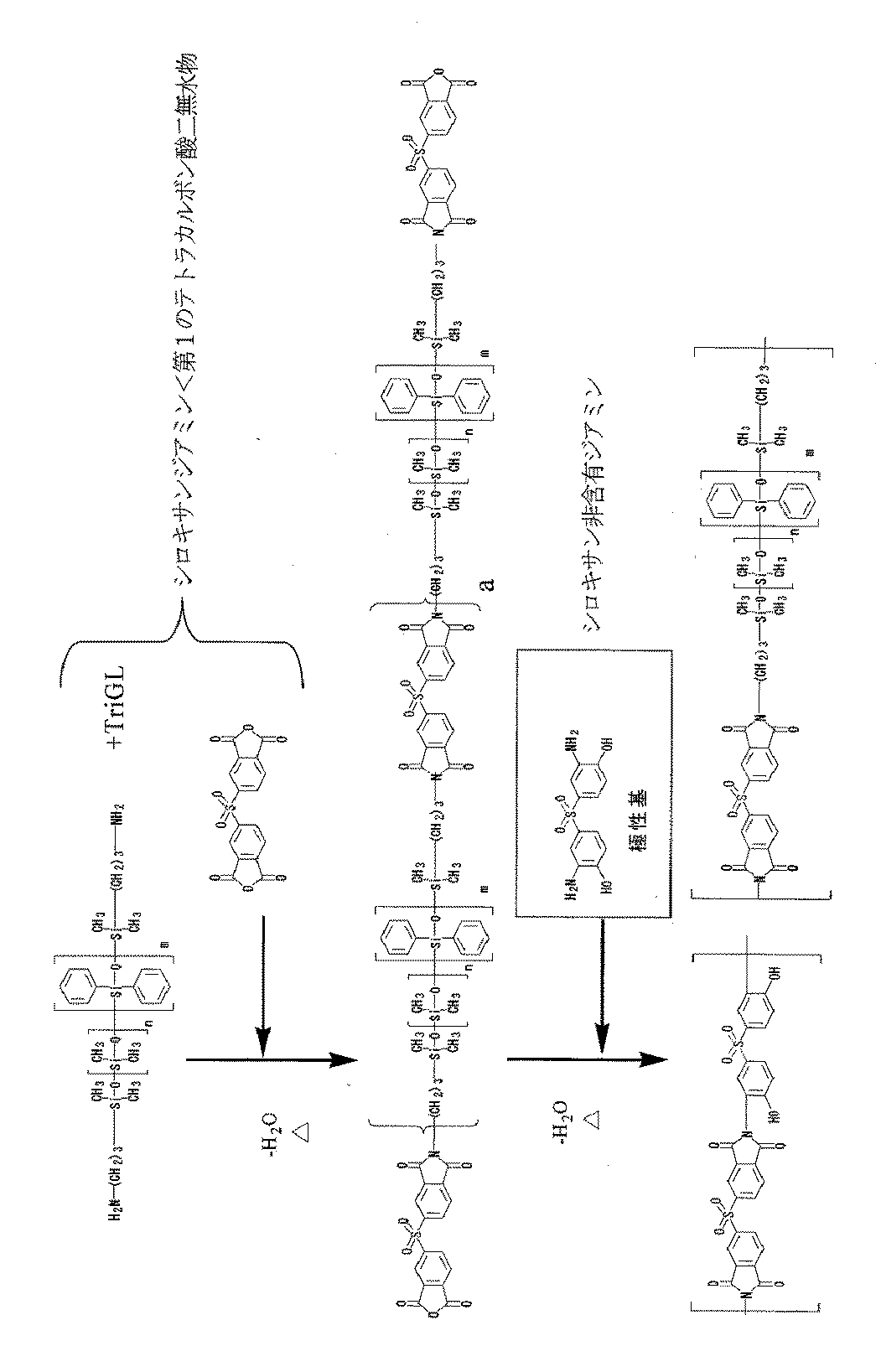
- the total acid dianhydride / total diamine ratio was 1.01. The synthesis route is shown below.
- Example 1 The siloxane residue-containing polyimide varnish prepared in Reference Example 1 was diluted with a mixed solvent of 9: 1 (mass ratio) of triglyme and ⁇ -butyrolactone so that the resin ratio was 48% by mass. The obtained diluted solution was coated and dried on a peeled PET (polyethylene terephthalate) film so as to have a dry thickness of 7 ⁇ m with a bar coater to form a protective layer with a peeled PET film.
- a mixed solvent of 9: 1 (mass ratio) of triglyme and ⁇ -butyrolactone so that the resin ratio was 48% by mass.
- the obtained diluted solution was coated and dried on a peeled PET (polyethylene terephthalate) film so as to have a dry thickness of 7 ⁇ m with a bar coater to form a protective layer with a peeled PET film.
- an epoxy resin mixture [mixture of 6 parts by mass of jER828US (Japan Epoxy Resin Co., Ltd.) and 2 parts by mass of jER807 (Japan Epoxy Resin Co., Ltd.)] 8 parts by mass of silver-coated copper particles (Ag Coat 1400 YP, Mitsui Kinzoku Kogyo Co., Ltd.) 78 parts by mass, 8 parts by mass of the siloxane residue-containing polyimide varnish of Reference Example 1, and 6 parts by mass of acid anhydride curing agent (Rikasit MH-700, Shin Nippon Rika Co., Ltd.)
- the resin solution obtained by diluting with a mixed solvent of triglyme and ⁇ -butyrolactone to a solid ratio of 93% by mass with a mixed solvent of 9: 1 (weight ratio) was dried with a bar coater on another peeled PET.
- a conductive adhesive layer with a release PET film was formed by coating and drying so that the thickness was 10
- the protective layer with the peeled PET film and the conductive adhesive layer with the peeled PET film obtained as described above are overlaid so that the respective peeled PET films are on the outside, and passed through a 120 ° C. thermal laminator, and both sides are peeled. A shield film sandwiched between PET films was obtained.
- Example 2 The size shown in Table 1 with respect to the ground wiring 32 as shown in FIG. 3 from the conductive adhesive layer side after peeling off the release PET film on the conductive adhesive layer side of the shield film obtained in Example 1. Is temporarily attached to the wiring board 31 having the cover coat layer 33 in which the ground opening 34 is formed, and the conductive adhesive layer is opened to the ground by a vacuum high temperature press (160 to 180 ° C., 1 to 4 MPa, 45 to 75 minutes). The shield film 35 was laminated
- a vacuum high temperature press 160 to 180 ° C., 1 to 4 MPa, 45 to 75 minutes.
- the conduction resistance value was measured.
- the obtained results are shown in Table 1.
- the conduction resistance value is desirably 1 ⁇ or less.
- the ground opening diameter is 0.2 mm, it is 1 ⁇ or less, indicating a good conduction resistance value, and it can be seen that the electromagnetic wave shielding is sufficiently performed.
- the shield film of the present invention does not use a phosphorus-containing epoxy resin for the binder resin of the conductive adhesive layer, there is no possibility that phosphorus will precipitate during solder reflow.
- a specific polyimide containing thermoplastic siloxane residue is used, even when the ground opening of the wiring board is small, it is easy to push into the ground opening, so the reliability of conduction between the ground circuit and the conductive adhesive layer And high electromagnetic shielding properties can be realized. Moreover, good flame retardancy can be achieved. Therefore, the shield film of the present invention is useful as an electromagnetic wave shielding material for various wiring boards.
Landscapes
- Chemical & Material Sciences (AREA)
- Chemical Kinetics & Catalysis (AREA)
- Organic Chemistry (AREA)
- Engineering & Computer Science (AREA)
- Medicinal Chemistry (AREA)
- Polymers & Plastics (AREA)
- Health & Medical Sciences (AREA)
- Materials Engineering (AREA)
- Life Sciences & Earth Sciences (AREA)
- Wood Science & Technology (AREA)
- Physics & Mathematics (AREA)
- Electromagnetism (AREA)
- Microelectronics & Electronic Packaging (AREA)
- Laminated Bodies (AREA)
- Shielding Devices Or Components To Electric Or Magnetic Fields (AREA)
- Macromolecular Compounds Obtained By Forming Nitrogen-Containing Linkages In General (AREA)
- Structure Of Printed Boards (AREA)
- Adhesives Or Adhesive Processes (AREA)
- Adhesive Tapes (AREA)
Abstract
ハンダリフロー時にリンの析出の可能性がなく、しかもグランド開口が小さい場合でも電磁波シールド性が損なわれないシールドフィルムは、保護層に、導電性フィラーがバインダー樹脂に分散してなる導電性接着層が積層されたものであり、バインダー樹脂がシロキサン残基含有ポリイミドを含有している。シロキサン残基含有ポリイミドは、式(A)の繰り返し構造単位を有する。(式中、nは1~30の整数であり、mは0~20の整数である。)
Description
本発明は、電磁波シールド性に優れたシールドフィルム、及びそのシールドフィルムが貼着されたシールド配線板に関する。
パーソナルコンピューター、携帯電話等の近年の精密電子機器は電磁波の影響を受けやすいため、機器内の各種配線板の回路形成面には、回路電磁波シールド性のシールドフィルムが貼着されている。ここで、配線板の回路形成面には、オーバーコート層が設けられており、そのオーバーコート層には、グランド回路とシールドフィルムとを導通させるためのグランド開口が形成されている。
このようなシールドフィルムとしては、配線板に貼着した後に最外表面に位置する絶縁層にシールド層が積層されたものが提案されている(特許文献1)。この特許文献1の実施例においては、シールド層として、エポキシ樹脂絶縁層に積層された銀蒸着層と、その銀蒸着層に、導電性フィラーとして銀コート銅粉20重量部を、難燃性で熱硬化性のリン含有エポキシ樹脂100重量部と、ノンハロゲン系の難燃剤10~180重量部とのブレンド物に均一に分散させて成膜した異方性導電接着層とからなるものが提案されている。
このようなシールドフィルムを配線板に貼着する場合、配線板の回路形成面にシールドフィルムの異方性導電接着層に積層し、熱プレスすることにより、異方性導電接着層を配線板のグランド開口に押し込みつつ硬化させ、それによりグランド回路と銀蒸着層とを導通させることにより、シールドフィルムの電磁波シールド性を実現している。
しかしながら、特許文献1のシールドフィルムの場合、ハンダリフロー処理時に、リンが析出し、配線や電子部品を損傷させることが懸念される。また、実装密度の向上とともに、グランド開口径が小さくなるため(例えば、0.2mm以下になるため)、異方性導電接着層を十分に押し込むことが困難となり、グランド回路と銀蒸着層との間の導通信頼性が低下し、電磁波シールド特性が低下することも懸念されている。
本発明の目的は、以上の従来の技術の課題を解決しようとするものであり、ハンダリフロー時にリンの析出の可能性がなく、しかもグランド開口が小さい場合でも電磁波シールド性が損なわれないシールドフィルムを提供することである。
本発明者らは、グランド開口径との関係で異方性導電接着層の使用に限界が生じていることから、絶縁性の保護層に、導電性フィラーがバインダー樹脂に分散してなる導電性接着層を設けた2層タイプのシールドフィルムにおいて、バインダー樹脂に、柔軟で押し込み性に富んだ熱可塑性樹脂の一種である特定のシロキサン残基含有ポリイミドを含有させることにより、上述の目的を達成できることを見出し、本発明を完成させた。
即ち、本発明は、保護層に、導電性フィラーがバインダー樹脂に分散してなる導電性接着層が積層されてなるシールドフィルムであって、バインダー樹脂がシロキサン残基含有ポリイミドを含有することを特徴とするシールドフィルムを提供する。
また、本発明は、上述のシールドフィルムの製造方法であって、以下の工程:
第1の剥離基材に保護層形成用塗料を塗布し、乾燥することにより保護層を形成する工程;
第2の剥離基材に、シロキサン残基含有ポリイミドを含有するバインダー樹脂と導電性フィラーとを含有する導電性接着層形成用塗料を塗布し、乾燥することにより導電性接着層を形成する工程;
保護層と導電性接着層とを互いに貼り合わせることによりシールドフィルムを形成する工程
を有することを特徴とする製造方法を提供する。
第1の剥離基材に保護層形成用塗料を塗布し、乾燥することにより保護層を形成する工程;
第2の剥離基材に、シロキサン残基含有ポリイミドを含有するバインダー樹脂と導電性フィラーとを含有する導電性接着層形成用塗料を塗布し、乾燥することにより導電性接着層を形成する工程;
保護層と導電性接着層とを互いに貼り合わせることによりシールドフィルムを形成する工程
を有することを特徴とする製造方法を提供する。
更に、本発明は、グランド配線が形成された配線板上に、グランド配線と導通するように、上述のシールドフィルムが、その導電性接着層により積層されていることを特徴とするシールド配線板を提供する。
本発明のシールドフィルムは、導電性接着層のバインダー樹脂に、リン含有エポキシ樹脂を使用しないので、ハンダリフロー時にリンが析出する可能性はない。また、熱可塑性の特定のシロキサン残基含有ポリイミドを使用しているので、配線板のグランド開口が小さい場合でも、グランド開口に押し込み易いため、グランド回路と導電性接着層との間の導通信頼性が高く、良好な電磁波シールド性を実現することができる。しかも、良好な難燃性を実現することができる。
以下、本発明を図面を参照しながら説明する。図1は、本発明のシールドフィルム10の断面図である。このシールドフィルム10は、保護層1に、導電性フィラー2がバインダー樹脂3に分散してなる導電性接着層4が積層された構造を有し、バインダー樹脂3がシロキサン残基含有ポリイミドを含有することを特徴としている。
(I)保護層1
本発明のシールドフィルム10を構成する保護層1は、シールドフィルムを配線板などの被着体に適用した際に、外表面に位置するものであり、被着体の外部から力や湿度などから保護する機能を有するものであり、前述した導電性接着層4の支持体としても機能するものである。
本発明のシールドフィルム10を構成する保護層1は、シールドフィルムを配線板などの被着体に適用した際に、外表面に位置するものであり、被着体の外部から力や湿度などから保護する機能を有するものであり、前述した導電性接着層4の支持体としても機能するものである。
このような保護層1としては、従来のシールドフィルム10における保護層と同じ構成を採用することができる。例えば、厚さ5~15μmの樹脂フィルム、例えば、ポリエステルフィルム、ポリイミドフィルム、ポリエーテルフィルム、ポリフェニレンサルファイドフィルム等を使用することができる。中でも、難燃性、柔軟性、可撓性の点から、後述する導電性接着層4のバインダー樹脂を構成するシロキサン残基含有ポリイミドを成膜したものを好ましく使用することができる。この場合、シロキサン残基含有ポリイミド単独で成膜することが好ましいが、シロキサン残基含有ポリイミドを含有するバインダー樹脂から成膜したものでもよい。
(II)導電性接着層4
本発明のシールドフィルム10を構成する導電性接着層4は、シールドフィルム10を配線板などの被着体に貼着させ、且つ電磁波シールド性を発揮する層である。
本発明のシールドフィルム10を構成する導電性接着層4は、シールドフィルム10を配線板などの被着体に貼着させ、且つ電磁波シールド性を発揮する層である。
このような導電性接着層4の厚みは、薄すぎると導電性とシールド性とが不十分となり、厚過ぎると柔軟性と可撓性とが低下するので、好ましくは5~20μm、より好ましくは7~15μmである。
(IIA)バインダー樹脂3を構成するシロキサン残基含有ポリイミド
上述したように、本発明では、シロキサン残基含有ポリイミドを導電性接着層に配合するが、この樹脂は熱可塑性であり、しかも溶融時の流動性向上に寄与するシロキサン残基を有する。また、難燃性に寄与するイミド結合とベンゼン環とを有している。従って、本発明のシールドフィルムは、ハンダリフロー時にリンが析出する可能性はない。また、配線板のグランド開口が小さい場合でも、グランド回路と導電性接着層との間の導通信頼性を向上させることができ、良好な電磁波シールド性を実現することができる。しかも、良好な難燃性を実現することができる。
上述したように、本発明では、シロキサン残基含有ポリイミドを導電性接着層に配合するが、この樹脂は熱可塑性であり、しかも溶融時の流動性向上に寄与するシロキサン残基を有する。また、難燃性に寄与するイミド結合とベンゼン環とを有している。従って、本発明のシールドフィルムは、ハンダリフロー時にリンが析出する可能性はない。また、配線板のグランド開口が小さい場合でも、グランド回路と導電性接着層との間の導通信頼性を向上させることができ、良好な電磁波シールド性を実現することができる。しかも、良好な難燃性を実現することができる。
本発明において、好ましいシロキサン残基含有ポリイミドとしては、式(A)の繰り返し構造単位を有するものが挙げられる。

式(A)中、nは1~30の整数、好ましくは1~20の整数であり、mは0~20の整数、好ましくは1~20の整数である。難燃性が特に必要ない場合には、シロキサンジアミンとしてmが0のものを使用し、難燃性が必要な場合はmが1以上のものを使用することが好ましい。式(A)のシロキサン残基含有ポリイミドの具体例としては、m=0として、X-22-161A、X-22-161B、KF8008、KF8012(以上、信越化学工業社)、BY16-871、BY16-853C、BY16-853u(以上、東レ・ダウコーニング社)、サイラエースFM3311(チッソ社)等を挙げることができ、m>1として、X-22-1660B3(信越化学工業社)等を挙げることができる。
このような式(A)のシロキサン残基含有ポリイミドのシロキサン残基は、好ましくはポリイミドを製造する際のシロキサンジアミン成分に由来するものであり、具体的には式(1)のシロキサンジアミンに由来するものである。なお、式(1)中、n、mは式(A)において説明したとおりである。このようなシロキサンジアミンの具体例としては、信越化学工業社製のKF-8010(m=0)、X-22-9409(m>1)を挙げることができる。なお、シロキサンジアミンとして、アミノ基がtert-ブトキシカルボニル基などのカルバメート系、フタロイル基などのイミド系、p-トルエンスルホニル基などのスルホンアミド系により保護されているものも使用できる。

本発明のシールドフィルム10の導電性接着層4におけるシロキサン残基含有ポリイミドの含有量は、少なすぎるとグランド開口への押し込みが困難となり、多すぎると相対的に導電性フィラーの含有量が減じ、いずれも導通信頼性が低下するので、好ましくは4~12質量%、より好ましくは6~9質量%である。
(IIB)シロキサン残基含有ポリイミドの製造方法
本発明で使用するシロキサン残基含有ポリイミドとしては、公知の方法で製造したものを使用することもできるが、少なくともテトラカルボン酸二無水物とシロキサンジアミンとを反応させてシロキサンポリイミド樹脂を製造する方法により得られたものを好ましく使用することができる。具体的には、以下の工程(a)~(c)を有する製造方法により得られたものを好ましく使用することができる。
本発明で使用するシロキサン残基含有ポリイミドとしては、公知の方法で製造したものを使用することもできるが、少なくともテトラカルボン酸二無水物とシロキサンジアミンとを反応させてシロキサンポリイミド樹脂を製造する方法により得られたものを好ましく使用することができる。具体的には、以下の工程(a)~(c)を有する製造方法により得られたものを好ましく使用することができる。
(a)溶媒中で第1のテトラカルボン酸二無水物とシロキサンジアミンとを還流条件下でイミド化反応させて酸無水物末端又はアミン末端シロキサンイミドオリゴマーを含む反応混合物を得る工程;
(b)工程(a)で得られた反応混合物を減圧濃縮して反応濃縮物を得る工程;及び
(c)工程(b)で得られた反応濃縮物に、溶媒とシロキサン非含有ジアミンとを添加し、シロキサン非含有ジアミンと反応濃縮物中の酸無水物末端シロキサンイミドオリゴマーとをイミド化反応させ、又は溶媒と第2のテトラカルボン酸二無水物とを添加し、第2のテトラカルボン酸二無水物と反応濃縮物中のアミン末端シロキサンイミドオリゴマーとをイミド化反応させ、それによりシロキサンポリイミド樹脂を得る工程。
(b)工程(a)で得られた反応混合物を減圧濃縮して反応濃縮物を得る工程;及び
(c)工程(b)で得られた反応濃縮物に、溶媒とシロキサン非含有ジアミンとを添加し、シロキサン非含有ジアミンと反応濃縮物中の酸無水物末端シロキサンイミドオリゴマーとをイミド化反応させ、又は溶媒と第2のテトラカルボン酸二無水物とを添加し、第2のテトラカルボン酸二無水物と反応濃縮物中のアミン末端シロキサンイミドオリゴマーとをイミド化反応させ、それによりシロキサンポリイミド樹脂を得る工程。
以下に工程毎に説明するが、この製造方法の効果について付言しておく。即ち、この製造方法においては、ジアミン成分のうちシロキサンジアミンを、まず、テトラカルボン酸二無水物成分とイミド化反応させて酸無水物末端又はアミン末端シロキサンイミドオリゴマーを得ておき、その反応終了後に、減圧下で溶媒と共に環状シロキサンオリゴマー等の揮発性不純物を除去する。このため、6量体までの環状のシロキサンオリゴマーのみならず、ブリードアウトする7量体以上のシロキサンオリゴマーや遊離シロキサン化合物を除去することができる。従って、酸無水物末端又はアミン末端シロキサンイミドオリゴマーに対し、追加的にシロキサン非含有ジアミン又はテトラカルボン酸二無水物をイミド化反応させる際に、シロキサンポリイミド樹脂の特性に影響を与えるような環状シロキサンオリゴマーの開環は生じない。よって、この製造方法で得られるシロキサン残基含有ポリイミドを使用したシールドフィルムは、環状シロキサンオリゴマーのブリードアウト現象が防止され、また、再加熱の際の環状シロキサンオリゴマー由来のアウトガスの発生量が大きく低減されているので、様々な電子部品用の配線板の電磁波シールド用途に好適なものとなる。
工程(a)
まず、溶媒中で第1のテトラカルボン酸二無水物とシロキサンジアミンとを還流条件下でイミド化反応させて酸無水物末端又はアミン末端シロキサンイミドオリゴマーを含む反応混合物を得る。
まず、溶媒中で第1のテトラカルボン酸二無水物とシロキサンジアミンとを還流条件下でイミド化反応させて酸無水物末端又はアミン末端シロキサンイミドオリゴマーを含む反応混合物を得る。
酸無水物末端シロキサンイミドオリゴマーを得るためには、シロキサンジアミンよりも第1のテトラカルボン酸二無水物のモル量を多くすればよい。逆に、アミン末端シロキサンイミドオリゴマーを得るためには、シロキサンジアミンよりも第1のテトラカルボン酸二無水物のモル量を少なくすればよい。ただし、シロキサンジアミンの使用量は、全テトラカルボン酸二無水物1モルに対し、少なすぎると接着性、可撓性の維持が困難になる傾向があり、多すぎると耐熱性が低下する傾向があるので、好ましくは、0.1~0.9モル、より好ましくは、0.3~0.8モルである。
工程(a)において、イミド化反応を還流条件下で行う理由は、ディーンスターク分離管等を用いてイミド化水を溶媒と共沸させて除くためである。従って、溶媒としては、テトラカルボン酸二無水物とシロキサンジアミンとの間のイミド化反応が生ずる温度で還流する溶媒であって、共沸により水を分離できる溶媒を使用する。このような溶媒としては、ジグライム、トリグライム等のグライム類、ジオキサン、テトラヒドロフラン等のエーテル系溶媒や、γ-ブチロラクトン、γ-バレロラクトン等のラクトン系溶媒、それらの混合物を使用することができる。また、発明の効果を損なわない限り、トルエン、キシレン、ベンゼン、メシチレン等の非極性溶媒、N-メチル-2-ピロリドン等の溶媒を併用してもよい。本工程(a)では、還流温度等の点から好ましくはグライム類と非極性溶媒との混合溶媒、中でもトリグライムと、ベンゼン、トルエン、キシレン及びメシチレンからなる群より選択される少なくとも一種との混合溶媒(w/w=1/(0.1~10))を好ましく使用できる。
工程(a)における溶媒の使用量は、溶媒や反応基質の種類により異なるが、少なすぎるとモノマー分散不良や還流効率の低下を引き起こし、多すぎると溶媒の気化熱が大きくなり反応槽内の温度が上がりにくくなるので、第1のテトラカルボン酸二無水物とシロキサンジアミンとの合計の質量が5~60質量%となる量で使用することが好ましい。
イミド化反応の反応温度は、溶媒や反応基質の種類や使用量により異なるが、低すぎるとイミド化反応が完結せず、高すぎるとイミド化反応以外の副反応が生じる可能性があるので、好ましくは150~220℃、より好ましくは160~200℃である。反応時間は、理論量のイミド化水を除去するに要した時間であり、通常0.5~12時間、好ましくは1~8時間である。
本発明で使用する第1のテトラカルボン酸二無水物の具体例としては、ピロメリット酸二無水物、3,4,3′,4′-ビフェニルテトラカルボン酸二無水物、4,4′-オキシジフタル酸二無水物、3,4,3′,4′-ベンゾフェノンテトラカルボン酸二無水物、3,3′,4,4′-ジフェニルスルホンテトラカルボン酸二無水物、9,9-ビス(3,4-ジカルボキシフェニル)フルオレン二無水物、9,9-ビス[4-(3,4-ジカルボキシフェノキシ)フェニル]フルオレン二無水物、2,3,6,7-ナフタレンテトラカルボン酸二無水物、4,4′-(ヘキサフルオロイソプロピリデン)ジフタル酸無水物、1,2,3,4-シクロブタンテトラカルボン酸二無水物、ビシクロ[2.2.2]オクト-7-エン-2,3,5,6-テトラカルボン酸二無水物、エチレングリコールビストリメリート二無水物、2,2-ビス(4-(3,4-ジカルボキシフェノキシ)フェニル)プロパン二無水物等を挙げることができる。中でも、3,3′,4,4′-ジフェニルスルホンテトラカルボン酸二無水物を好ましく使用できる。
本発明で使用するシロキサンジアミンとしては、少なくとも分子内にジメチルシリレン骨格を有する化合物であり、従来より、ポリイミド樹脂のシロキサン変性に用いられているものを使用できる。中でも、難燃性、相溶性確保の点から前述した式(1)の構造を有するものを好ましく使用できる。
なお、工程(a)におけるイミド化の際に、必要に応じてトリエチルアミン等の3級アミン、芳香族系イソキノリン、ピリジン等の塩基性触媒や、安息香酸、パラヒドロキシ安息香酸などの酸触媒を添加してもよい。
工程(b)
工程(a)の反応終了後、工程(a)で得られた反応混合物を減圧濃縮して反応濃縮物を得る。この工程(b)は、工程(a)で使用するシロキサンジアミン中に環状シロキサンオリゴマーが不純物として含有されていた場合に、その環状シロキサンオリゴマーを除去する工程となる。即ち、減圧濃縮することにより、溶媒と微量の水と共に、揮発性の環状シロキサンオリゴマー、更に遊離シロキサン化合物(例えば低分子量シロキサンモノアミン、低分子量シロキサン)とを効率よく除去することができる。この減圧濃縮の際の温度は、低すぎると環状シロキサンオリゴマーまたは遊離シロキサン化合物の除去効率が悪化するので、工程(a)のイミド化反応温度と同温または、大気圧での溶剤沸点温度とすることが好ましい。
工程(a)の反応終了後、工程(a)で得られた反応混合物を減圧濃縮して反応濃縮物を得る。この工程(b)は、工程(a)で使用するシロキサンジアミン中に環状シロキサンオリゴマーが不純物として含有されていた場合に、その環状シロキサンオリゴマーを除去する工程となる。即ち、減圧濃縮することにより、溶媒と微量の水と共に、揮発性の環状シロキサンオリゴマー、更に遊離シロキサン化合物(例えば低分子量シロキサンモノアミン、低分子量シロキサン)とを効率よく除去することができる。この減圧濃縮の際の温度は、低すぎると環状シロキサンオリゴマーまたは遊離シロキサン化合物の除去効率が悪化するので、工程(a)のイミド化反応温度と同温または、大気圧での溶剤沸点温度とすることが好ましい。
減圧濃縮の際の圧力は、減圧度が十分でないと環状シロキサンオリゴマーまたは遊離シロキサン化合物の除去効率が悪化し、逆に減圧しすぎることは処理コストの過度の増大を招くので、好ましくは0.3~91kPa、より好ましくは11~51kPaである。
工程(c)
次に、工程(b)で得られた反応濃縮物が酸無水物末端シロキサンイミドオリゴマーである場合には、反応濃縮物に、溶媒とシロキサン非含有ジアミンとを添加し、シロキサン非含有ジアミンと酸無水物末端シロキサンイミドオリゴマーとをイミド化反応させ、それによりシロキサンポリイミド樹脂を得る。この場合、必要に応じてシロキサン非含有ジアミンと共に第2のテトラカルボン酸二無水物を添加してもよい。
次に、工程(b)で得られた反応濃縮物が酸無水物末端シロキサンイミドオリゴマーである場合には、反応濃縮物に、溶媒とシロキサン非含有ジアミンとを添加し、シロキサン非含有ジアミンと酸無水物末端シロキサンイミドオリゴマーとをイミド化反応させ、それによりシロキサンポリイミド樹脂を得る。この場合、必要に応じてシロキサン非含有ジアミンと共に第2のテトラカルボン酸二無水物を添加してもよい。
または、反応濃縮物がアミン末端シロキサンイミドオリゴマーである場合には、反応濃縮物に、溶媒と第2のテトラカルボン酸二無水物とを添加し、第2のテトラカルボン酸二無水物と反応濃縮物中のアミン末端シロキサンイミドオリゴマーとをイミド化反応させ、それによりシロキサンポリイミド樹脂を得る。この場合、必要に応じて第2のテトラカルボン酸二無水物と共にシロキサン非含有ジアミンを添加してもよい。
工程(b)の後で溶媒を添加するのは、溶剤調整のためであり、その工程によりポリイミド固形分濃度を調整する事が可能となる。溶媒としては、工程(a)で用い得るものを使用できる。特に、シロキサンポリイミド樹脂をワニスとして使用する場合には、コーティング時の吸湿によるポリイミド析出を防ぐために、比較的吸湿性の低い溶媒であるエーテル系溶媒、ラクトン系溶媒、非極性溶媒などを単独、または混合して使用することができる。特に、本工程(c)では、トリグライム(別名:トリエチレングリコールジメチルエーテル)とγ-ブチロラクトンとの混合溶媒(w/w=1/(0.1~10))を好ましく使用できる。
工程(c)において使用する“シロキサン非含有ジアミン”としては、分子内にジメチルシリレン骨格を持たないジアミンを使用することができ、その具体例としては、3,3′-ジアミノ-4,4′-ジヒドロキシジフェニルスルホン、2,2-ビス(3-アミノ-4-ヒドロキシフェニル)ヘキサフルオロプロパン、2,2-ビス(3-アミノ-4-ヒドロキシフェニル)プロパン、3,3′-ジアミノ-4,4′-ジヒドロキシジフェニルメタン、3,3′-ジヒドロキシ-4,4′-ジアミノビフェニル、2,4-ジアミノフェノール、9,9-ビス(3-アミノ-4-ヒドロキシフェニル)フルオレン等のジアミノフェノール誘導体;p-フェニレンジアミン、4,4′-ジアミノジフェニルエーテル、2,2-ビス[4-(4-アミノフェノキシ)フェニル]プロパン、ビス[4-(4-アミノフェノキシ)フェニル]スルホン、1,3-ビス(4-アミノフェノキシ)ベンゼン、2,2′-ビス(トリフルオロメチル)-4,4′-ジアミノビフェニル、1,3-ビス(3-アミノフェノキシ)ベンゼン、4,4′-ジアミノベンズアニリド、5,5′-メチレン-ビス(アントラニック酸)、9,9-ビス[4-(4-アミノフェノキシフェニル)]フルオレン、9,9-ビス(4-アミノフェノキシ)フルオレン、4,4′-ジアミノジフェニルスルホン、3,4′-ジアミノジフェニルエーテル、2,2-ビス[4-(4-アミノフェノキシ)フェニル]ヘキサフルオロプロパン、4,4′-ビス(4-アミノフェノキシ)ビフェニル、1,4-ビス(4-アミノフェノキシ)ベンゼン、o-トリジンスルホン等の芳香族ジアミン;trans-1,4-シクロヘキサンジアミン、cis-1,4-シクロヘキサンジアミン、4,4′-メチレンビス(シクロヘキシルアミン)等の脂肪族ジアミンを挙げることができるが、これらに限定されるものではない。
他方、“第2のテトラカルボン酸二無水物”としては、既に例示した第1のテトラカルボン酸二無水物と同様のものを使用することができる。ここで、第1のテトラカルボン酸二無水物と第2のテトラカルボン酸二無水物とは同一でも異なっていてもよい。
工程(b)で得られた反応濃縮物が酸無水物末端シロキサンイミドオリゴマーの場合、工程(c)で使用するシロキサン非含有ジアミンの使用量は、機械特性が十分なカバーレイを得るための分子量を確保するために、シロキサンジアミンと合算したモル数が、全テトラカルボン酸二無水物1モルに対して、好ましくは0.1~0.9モル、より好ましくは0.3~0.8モルとなる量である。
一方、工程(b)で得られた反応濃縮物がアミン末端シロキサンイミドオリゴマーの場合には、工程(c)で使用する第2のテトラカルボン酸二無水物の使用量は、機械特性が十分なカバーレイを得るための分子量を確保するために、第1のテトラカルボン酸二無水物と第2のテトラカルボン酸二無水物とを合算したモル数1モルに対して、シロキサンジアミンとシロキサン非含有ジアミンとを合算した全ジアミン成分が好ましくは0.8~1.2モル、より好ましくは0.9~1.1モルとなる量である。
なお、工程(c)におけるイミド化の際に、工程(a)の場合と同様に、必要に応じてトリエチルアミン等の3級アミン、芳香族系イソキノリン、ピリジン等の塩基性触媒や、安息香酸、パラヒドロキシ安息香酸などの酸触媒を添加してもよい。
工程(c)において極性基を有する酸二無水物やジアミン成分を使用した場合には、ワイゼルベルグ効果により生成したシロキサンポリイミド樹脂の粘度が増大し、撹拌棒の周囲に巻き付く現象が生ずることがある。生成したシロキサンポリイミド樹脂の粘度の増大を避けるためには、反応系中に水を存在させることが好ましい。この場合、水の量が少なすぎると増粘する危険性が高まり、多すぎるとポリイミドの分子量が低下する恐れがあるので、反応混合物中に0.01~1.1質量%の割合で水を存在させることが好ましい。
工程(c)におけるイミド化の際の反応温度は、溶媒や反応基質の種類や使用量により異なるが、低すぎるとイミド化反応が完結せず、高すぎるとイミド化反応以外の副反応が生じる可能性があるので、好ましくは、150~220℃、より好ましくは、160~200℃である。反応時間は、通常0.5~12時間、好ましくは、1~8時間である。これにより、環状シロキサンオリゴマーおよび遊離シロキサン化合物の含有量が少ないシロキサン残基含有ポリイミドがワニス状態で得られる。
本発明で使用するシロキサン残基含有ポリイミドは、図2に示す合成装置によりワンバッチで製造することが可能である。
図2はシロキサンポリイミド樹脂を製造するための合成装置の全体図である。この合成装置は、加熱装置21で加熱可能な反応容器22と、反応容器22の上方に装着された凝縮器23と、凝縮器23で凝縮した凝縮物をトラップする凝縮トラップ槽24と、反応容器22内にガスを導入するためのガス導入管25とを有する。凝縮トラップ槽24には貯留した凝縮物を系外に排出するためのドレイン24aが設置されている。凝縮トラップ槽24と反応容器22との間は、所定量以上の凝縮物が凝縮トラップ槽24に貯留された場合に、過剰の凝縮物を反応容器22に戻すためのオーバーフロー管26で連結されている。また、ガス導入管25はオーバーフロー管26のオーバーフロー面26aよりも下方に位置するように反応容器22に設置されている。更に、反応容器22には減圧装置27が連結されている。ここで、ガス導入管25を、オーバーフロー管26のオーバーフロー面26aよりも下方に位置するように反応容器22に設置する理由は、ガス導入管25から反応容器22内の反応混合物RMの液面近くに導入されたガスが、反応混合物RMの液面から揮発した環状シロキサンオリゴマーと水と溶媒とを、ガス流に乗せて効率良く凝縮器23へ導くことができるためである。また、反応容器22には撹拌装置28が設置されている。また、図示してはいないが温度測定装置も設置されている。
図2の合成装置を構成する個々の部品は、従来の化学反応装置で用いられているものを適宜選択して利用することができる。
(IIC)バインダー樹脂3のシロキサン残基含有ポリイミド以外の成分
(IICa)エポキシ樹脂とエポキシ樹脂用硬化剤
導電性接着層4を構成するバインダー樹脂3には、シールドフィルムの導通信頼性を確保すべく、熱硬化性を導電性接着層4に付与するために、種々の熱硬化性樹脂とそのための硬化剤とを配合することができる。特に好ましい熱硬化性樹脂としてエポキシ樹脂を使用することができる。エポキシ樹脂としては、ビスフェノールA型エポキシ樹脂、ビスフェノールF型エポキシ樹脂、ビスフェノールS型エポキシ樹脂、脂環式エポキシ樹脂等を使用することができる。これらは液状であっても固形状であってもよい。また、エポキシ樹脂用の硬化剤としては、公知の硬化剤(例えば、アミン系硬化剤、イミダゾール系硬化剤、ポリメルカプタン系硬化剤、酸無水物系硬化剤等)を挙げることができる。中でも、硬化温度が相対的に高いものの、ポットライフが比較的長く、バランスのよい電気的特性、化学的特性及び機械的特性の硬化物を与えることできる酸無水物系硬化剤(例えば、無水フタル酸等の芳香族酸無水物、テトラヒドロ無水フタル酸等の脂環式酸無水物、無水コハク酸等の脂肪族酸無水物)を好ましく使用することができる。中でも、室温で低粘度な液体であることから、脂環式酸無水物を好ましく使用することができる。
(IICa)エポキシ樹脂とエポキシ樹脂用硬化剤
導電性接着層4を構成するバインダー樹脂3には、シールドフィルムの導通信頼性を確保すべく、熱硬化性を導電性接着層4に付与するために、種々の熱硬化性樹脂とそのための硬化剤とを配合することができる。特に好ましい熱硬化性樹脂としてエポキシ樹脂を使用することができる。エポキシ樹脂としては、ビスフェノールA型エポキシ樹脂、ビスフェノールF型エポキシ樹脂、ビスフェノールS型エポキシ樹脂、脂環式エポキシ樹脂等を使用することができる。これらは液状であっても固形状であってもよい。また、エポキシ樹脂用の硬化剤としては、公知の硬化剤(例えば、アミン系硬化剤、イミダゾール系硬化剤、ポリメルカプタン系硬化剤、酸無水物系硬化剤等)を挙げることができる。中でも、硬化温度が相対的に高いものの、ポットライフが比較的長く、バランスのよい電気的特性、化学的特性及び機械的特性の硬化物を与えることできる酸無水物系硬化剤(例えば、無水フタル酸等の芳香族酸無水物、テトラヒドロ無水フタル酸等の脂環式酸無水物、無水コハク酸等の脂肪族酸無水物)を好ましく使用することができる。中でも、室温で低粘度な液体であることから、脂環式酸無水物を好ましく使用することができる。
バインダー樹脂が、シロキサン残基含有ポリイミドに加えてエポキシ樹脂とエポキシ樹脂用硬化剤とを併用する場合、シロキサン残基含有ポリイミド100質量部に対し、エポキシ樹脂を65~230質量部含むことが好ましく、100~140質量部含むことがより好ましい。また、エポキシ樹脂用硬化剤を45~150質量部含むことが好ましく、70~100質量部含むことがより好ましい。
(IICb)導電性フィラー
本発明において使用する導電性フィラー2としては、いわゆる導電ペーストに使用されているような導電性フィラーを使用することができる。例えば、扁平な銀、銅などの金属粉、銀コート銅粉等の金属コート金属粉、扁平スチレン粒子コアのNiコート、Auフラッシュメッキ物等の金属コート樹脂粉等を使用することができる。異方性導電接着剤において使用されているような球状の導電性粒子も使用することが可能である。両者を混合して使用してもよい。
本発明において使用する導電性フィラー2としては、いわゆる導電ペーストに使用されているような導電性フィラーを使用することができる。例えば、扁平な銀、銅などの金属粉、銀コート銅粉等の金属コート金属粉、扁平スチレン粒子コアのNiコート、Auフラッシュメッキ物等の金属コート樹脂粉等を使用することができる。異方性導電接着剤において使用されているような球状の導電性粒子も使用することが可能である。両者を混合して使用してもよい。
このような導電性フィラー2の平均粒子径は、小さすぎると導電性が不十分となり、大きすぎるとグランドへの押し込み性が悪くなるので、好ましくは2~20μm、より好ましくは5~10μmである。なお、導電性フィラーが扁平な場合、粒径は長径に相当し、厚みは長径の5~40%であることが好ましい。
導電性接着層4中における導電性フィラー2の含有量は、少な過ぎるとシールドフィルムの導通信頼性が不十分となり、多すぎると導電性接着層4自体の膜強度が低下するので、好ましくは65~85質量%、より好ましくは70~80質量%である。
(IICc)その他の成分
本発明における導電性接着層4には、本発明の効果を損なわない範囲で、ポリエステル、ポリアミド等の熱可塑性樹脂、着色剤、防腐剤、分散剤等を必要に応じて含有させることができる。
本発明における導電性接着層4には、本発明の効果を損なわない範囲で、ポリエステル、ポリアミド等の熱可塑性樹脂、着色剤、防腐剤、分散剤等を必要に応じて含有させることができる。
(IID)シールドフィルムの製造
本発明のシールドフィルムは、常法に従って製造することができる。例えば、シロキサン残基含有ポリイミド、導電性フィラー、更に必要に応じてエポキシ樹脂及びエポキシ樹脂用硬化剤をトルエン等の溶剤溶媒と共に、公知のミキサーを用いて均一に混合することにより導電性接着層形成用塗料を調製し、得られた塗料を、保護層1となる樹脂フィルムに塗布・乾燥することにより製造することができる。必要に応じ、シールドフィルムの導電性接着層側には剥離シートを積層しておくことができる。また、保護層1となる樹脂フィルムとして、剥離PET(ポリエチレンテレフタレート)フィルム上に、シロキサン残基含有ポリイミドやそれにエポキシ樹脂や他の熱可塑性樹脂を混合した樹脂液を塗布・乾燥することにより得た剥離PET付き保護層フィルムを使用することもできる。
本発明のシールドフィルムは、常法に従って製造することができる。例えば、シロキサン残基含有ポリイミド、導電性フィラー、更に必要に応じてエポキシ樹脂及びエポキシ樹脂用硬化剤をトルエン等の溶剤溶媒と共に、公知のミキサーを用いて均一に混合することにより導電性接着層形成用塗料を調製し、得られた塗料を、保護層1となる樹脂フィルムに塗布・乾燥することにより製造することができる。必要に応じ、シールドフィルムの導電性接着層側には剥離シートを積層しておくことができる。また、保護層1となる樹脂フィルムとして、剥離PET(ポリエチレンテレフタレート)フィルム上に、シロキサン残基含有ポリイミドやそれにエポキシ樹脂や他の熱可塑性樹脂を混合した樹脂液を塗布・乾燥することにより得た剥離PET付き保護層フィルムを使用することもできる。
また、本発明のシールドフィルムは、別法として、以下の工程:
第1の剥離基材に、保護層形成用塗料を塗布し、乾燥することにより保護層を形成する工程;
第2の剥離基材に、シロキサン残基含有ポリイミドを含有するバインダー樹脂と導電性フィラーとを含有する導電性接着層形成用塗料を塗布し、乾燥することにより導電性接着層を形成する工程;
保護層と導電性接着層とを互いに貼り合わせることによりシールドフィルムを形成する工程
を有する製造方法により製造することができる。
第1の剥離基材に、保護層形成用塗料を塗布し、乾燥することにより保護層を形成する工程;
第2の剥離基材に、シロキサン残基含有ポリイミドを含有するバインダー樹脂と導電性フィラーとを含有する導電性接着層形成用塗料を塗布し、乾燥することにより導電性接着層を形成する工程;
保護層と導電性接着層とを互いに貼り合わせることによりシールドフィルムを形成する工程
を有する製造方法により製造することができる。
第1の剥離基材としては、例えば、公知の剥離処理されたポリエステルフィルムやポリオレフィンフィルム、ナイロンフィルム等を使用することができる。保護層形成用塗料としては、絶縁性の樹脂系塗料を広く使用することができるが、本発明を特徴づけるシロキサン残基含有ポリイミドを、トリグライムやγ-ブチロラクトンなどの溶剤に溶解した塗料を、難燃性、柔軟性及び絶縁性の点で好ましく使用することができる。なお、保護層形成用塗料の塗布、乾燥は、公知の技術、条件を採用することができる。
第2の剥離基材としては、第1の剥離基材と同様のものを使用することができる。導電性接着層形成用塗料は、シロキサン残基含有ポリイミドを含有するバインダー樹脂と導電性フィラーとを、トリグライムやγ-ブチロラクトンなどの溶剤に溶解・分散したものである。導電性接着層形成用塗料の塗布・乾燥は、公知の技術、条件を採用することができる。
保護層と導電性接着層との貼り合わせは、好ましくは100~130℃の熱ラミネーター、熱プレス板で行うことができる。
具体的なシールドフィルムの製造例としては、まず、シリコーン剥離処理済みPETフィルム上に、シロキサン残基含有ポリイミドワニスやそれにエポキシ樹脂や他の熱可塑性樹脂を混合した樹脂液を、バーコーターで塗布し、100~150℃の乾燥炉に投入して乾燥することにより剥離PET付き保護層1を形成する。それとは別に、剥離PETフィルム上に、導電性接着層形成用ワニスを塗布・乾燥することにより、剥離PET付き導電性接着層4を形成する。そして、保護層1と導電性接着層4とを互いに重ね、100~130℃の熱ラミネーターで貼り合わせることにより両面が剥離PETフィルムで挟持されたシールドフィルムを製造することができる。このようなシールドフィルムは、導電性接着層側の剥離PETフィルムを剥離し、導電性接着層を被着体に接触させ、熱プレスすることにより使用される。
(III)シールド配線板
以上説明した本発明のシールドフィルムは、グランド配線が形成された配線板を電磁波シールドするために好ましく使用することができる。図3にシールド配線板30の平面透視図を示す。このシールド配線板30は、フレキシブル基板、ガラスエポキシ基板等の公知の配線板31上にグランド配線32が形成されており、更にその上にポリイミドフィルムなどの厚さ10~37μmのカバーコート層33が積層されている。カバーコート層33には、グランド配線32まで、0.2~1.8μm径のグランド開口34が形成されている。そして、配線板31のカバーコート層33に対し、シールドフィルム35が、その導電性接着層側から熱プレスにより貼着され且つグランド開口34に押しこまれている。また、配線板31の端部には導通計測用開口36が形成されている。
以上説明した本発明のシールドフィルムは、グランド配線が形成された配線板を電磁波シールドするために好ましく使用することができる。図3にシールド配線板30の平面透視図を示す。このシールド配線板30は、フレキシブル基板、ガラスエポキシ基板等の公知の配線板31上にグランド配線32が形成されており、更にその上にポリイミドフィルムなどの厚さ10~37μmのカバーコート層33が積層されている。カバーコート層33には、グランド配線32まで、0.2~1.8μm径のグランド開口34が形成されている。そして、配線板31のカバーコート層33に対し、シールドフィルム35が、その導電性接着層側から熱プレスにより貼着され且つグランド開口34に押しこまれている。また、配線板31の端部には導通計測用開口36が形成されている。
このシールド配線板30は、ハンダリフロー処理されてもリンが析出することはなく、また、異方性導電接着剤を使用せずに、熱可塑性の特定のシロキサン残基含有ポリイミドを使用しているので、導電性接着層がグランド開口に十分に押し込むことができ、良好な磁波シールド性が実現される。また、難燃性も良好なものとなる。
このようなシールド配線板30は、例えば、両面が剥離PETフィルムで挟持されたシールドフィルムを使用して製造することができる。即ち、両面が剥離PETフィルムで挟持されたシールドフィルムの導電性接着層側の剥離PETフィルムを剥離し、導電性接着層を基板のグランド配線側に重ね、剥離PETフィルム側から熱プレスすることにより製造することができる。最後に、表面の剥離PETフィルムを取り去ればよい。
以下、本発明を実施例により具体的に説明する。
参考例1(酸無水物末端シロキサンイミドオリゴマーを経由してシロキサン残基含有ポリイミドを合成する例)
図2のシロキサン残基含有ポリイミド用合成装置の反応容器(20L)に、4372.65g(3.24mol)のジアミノシロキサン(アミン当量675g/mol、X-22-9409、信越化学工業社製)と、1994.54g(5.54mol)の3,3′,4,4′-ジフェニルスルホンテトラカルボン酸二無水物(リカシッドDSDA、新日本理化社製;純度99.6%)と、3000gのトリグライムと、1100gのトルエンとを投入し、混合物を2時間十分に撹拌した。その後、185℃まで昇温させ、2時間その温度を保ち、凝縮トラップ槽で水を回収しながら、反応液を還流撹拌した。
図2のシロキサン残基含有ポリイミド用合成装置の反応容器(20L)に、4372.65g(3.24mol)のジアミノシロキサン(アミン当量675g/mol、X-22-9409、信越化学工業社製)と、1994.54g(5.54mol)の3,3′,4,4′-ジフェニルスルホンテトラカルボン酸二無水物(リカシッドDSDA、新日本理化社製;純度99.6%)と、3000gのトリグライムと、1100gのトルエンとを投入し、混合物を2時間十分に撹拌した。その後、185℃まで昇温させ、2時間その温度を保ち、凝縮トラップ槽で水を回収しながら、反応液を還流撹拌した。
反応液の温度185℃に保持したまま、系内の圧力を11KPaまで減圧し、溶媒、水、環状シロキサンオリゴマーを含有する減圧回収物Aを取得すると共に、反応濃縮物(酸無水物末端シロキサンイミドオリゴマー)を得た。酸化皮膜が除去されたシリコンウェハー上にオリゴマー溶液を塗布し、100℃で10分間乾燥させFT-IR透過法によって末端官能基の同定を行った。1780cm-1付近にイミドカルボニルの吸収が出現し、1860cm-1付近に環状酸無水物カルボニル伸縮振動の吸収が確認できる事から酸無水物末端シロキサンイミドオリゴマーの生成が確認できた。
反応濃縮物を80℃まで放冷し、反応濃縮物に632.81g(2.25mol)の3,3′-ジアミノ-4,4′-ジヒドロキシジフェニルスルホン(BSDA、小西化学工業製;純度99.7%)と、3300gのトリグライム(TriGL)と700gのγ-ブチロラクトンとを投入し、室温で12時間攪拌した。攪拌後、185℃まで昇温し、その温度で2時間加熱攪拌した。その後、室温まで冷却し、シロキサン残基含有ポリイミドのワニスを得た。本参考例では、全酸二無水物/全ジアミン比は1.01であった。合成経路については以下に示す。
実施例1
参考例1で調製したシロキサン残基含有ポリイミドワニスを、トリグライムとγ-ブチロラクトンとの9:1(質量比)の混合溶媒で樹脂割合が48質量%となるように希釈した。得られた希釈液は、剥離PET(ポリエチレンテレフタレート)フィルム上に、バーコーターで乾燥厚が7μmとなるように塗布・乾燥することにより剥離PETフィルム付き保護層を形成した。
参考例1で調製したシロキサン残基含有ポリイミドワニスを、トリグライムとγ-ブチロラクトンとの9:1(質量比)の混合溶媒で樹脂割合が48質量%となるように希釈した。得られた希釈液は、剥離PET(ポリエチレンテレフタレート)フィルム上に、バーコーターで乾燥厚が7μmとなるように塗布・乾燥することにより剥離PETフィルム付き保護層を形成した。
これとは別に、エポキシ樹脂混合物[6質量部のjER828US(ジャパンエポキシレジン社)および2質量部のjER807(ジャパンエポキシレジン社)の混合物]8質量部、平均粒径7μmの銀コート銅粒子(Agコート1400YP、三井金属工業社)78質量部、参考例1のシロキサン残基含有ポリイミドワニス8質量部、および酸無水物系硬化剤(リカシットMH-700、新日本理化社)6質量部の混合物を、トリグライムとγ-ブチロラクトンとの9:1(重量比)の混合溶媒で、固形割合が93質量%となるように希釈して得た樹脂液を、別の剥離PET上に、バーコーターで乾燥厚が10μmとなるように塗布・乾燥することにより剥離PETフィルム付き導電性接着層を形成した。
上述したように得られた剥離PETフィルム付き保護層と剥離PETフィルム付き導電性接着層とを、それぞれの剥離PETフィルムが外側になるように重ね、120℃の熱ラミネーターを通過させ、両面が剥離PETフィルムで挟持されたシールドフィルムを得た。
実施例2
実施例1で得られたシールドフィルムを、導電性接着層側の剥離PETフィルムを剥がした後に、導電性接着層側から、図3に示すような、グランド配線32に対して表1に示す大きさのグランド開口34が形成されたカバーコート層33を有する配線板31に仮貼りし、真空高温プレス(160~180℃、1~4MPa、45~75分)により、導電性接着層をグランド開口34内に押し込みつつ熱硬化させることにより配線板31上にシールドフィルム35を積層し、シールド配線板を得た。ここで、カバーコート層33の両端部に、導通計測用開口36を形成した。なお、各開口底部のグランド配線には、1~6μm厚の無電解ニッケルメッキ層を形成し、更に0.03~0.15μm厚の無電解金メッキ層を形成した。
実施例1で得られたシールドフィルムを、導電性接着層側の剥離PETフィルムを剥がした後に、導電性接着層側から、図3に示すような、グランド配線32に対して表1に示す大きさのグランド開口34が形成されたカバーコート層33を有する配線板31に仮貼りし、真空高温プレス(160~180℃、1~4MPa、45~75分)により、導電性接着層をグランド開口34内に押し込みつつ熱硬化させることにより配線板31上にシールドフィルム35を積層し、シールド配線板を得た。ここで、カバーコート層33の両端部に、導通計測用開口36を形成した。なお、各開口底部のグランド配線には、1~6μm厚の無電解ニッケルメッキ層を形成し、更に0.03~0.15μm厚の無電解金メッキ層を形成した。
<評価>
導通抵抗値測定
実施例2で得られたシールド配線板について、導通抵抗値を測定した。得られた結果を表1に示す。実用上、導通抵抗値は1Ω以下であることが望ましい。表1からわかるように、グランド開口径が0.2mmであっても1Ω以下であり、良好な導通抵抗値を示しており、十分に電磁波シールドされていることがわかる。
導通抵抗値測定
実施例2で得られたシールド配線板について、導通抵抗値を測定した。得られた結果を表1に示す。実用上、導通抵抗値は1Ω以下であることが望ましい。表1からわかるように、グランド開口径が0.2mmであっても1Ω以下であり、良好な導通抵抗値を示しており、十分に電磁波シールドされていることがわかる。

難燃性試験(UL-94 VTM試験)
20μm厚のポリイミドフィルム(エスパネックMシリーズ、新日鐵化学社)の両面に、実施例1のシールドフィルムを仮貼りし、真空高温プレス(160~180℃、1~4MPa、45~75分)により貼り合わせた試験シートを作成し、それに対しUL-94のVTM試験を行った。その結果VTM-0を達成し、良好な難燃性を示した。
20μm厚のポリイミドフィルム(エスパネックMシリーズ、新日鐵化学社)の両面に、実施例1のシールドフィルムを仮貼りし、真空高温プレス(160~180℃、1~4MPa、45~75分)により貼り合わせた試験シートを作成し、それに対しUL-94のVTM試験を行った。その結果VTM-0を達成し、良好な難燃性を示した。
シールド効果測定
難燃性試験で作成したものと同一の試験シートを作成し、KEC法(関西電子工業振興センター法)でシールド効果の測定を行った。得られた結果を図4に示す。対照として18μm厚の銅箔のシールド効果測定結果も併せて図4に示す。図4の結果から、実施例1のシールドフィルムは、70MHz付近までは、銅箔と同等の良好なシールド効果を有していることがわかる。
難燃性試験で作成したものと同一の試験シートを作成し、KEC法(関西電子工業振興センター法)でシールド効果の測定を行った。得られた結果を図4に示す。対照として18μm厚の銅箔のシールド効果測定結果も併せて図4に示す。図4の結果から、実施例1のシールドフィルムは、70MHz付近までは、銅箔と同等の良好なシールド効果を有していることがわかる。
参考例1のシロキサン残基含有ポリイミド製造時の常圧回収物Aの分析
減圧回収物Aを、GC-MS(6890/5973GC-MS、Agilent社製)を用いて測定した。得られた結果を図5に示す。これらの図から解るように、3~6量体の環状シロキサンオリゴマーだけでなく、7量体(D7)の環状シロキサンオリゴマーや更に分子量の大きい遊離シロキサン化合物までも回収除去できたことが解る。
減圧回収物Aを、GC-MS(6890/5973GC-MS、Agilent社製)を用いて測定した。得られた結果を図5に示す。これらの図から解るように、3~6量体の環状シロキサンオリゴマーだけでなく、7量体(D7)の環状シロキサンオリゴマーや更に分子量の大きい遊離シロキサン化合物までも回収除去できたことが解る。
本発明のシールドフィルムは、導電性接着層のバインダー樹脂に、リン含有エポキシ樹脂を使用しないので、ハンダリフロー時にリンが析出する可能性はない。また、熱可塑性の特定のシロキサン残基含有ポリイミドを使用しているので、配線板のグランド開口が小さい場合でも、グランド開口に押し込み易いため、グランド回路と導電性接着層との間の導通信頼性が高く、良好な電磁波シールド性を実現することができる。しかも、良好な難燃性を実現することができる。従って、本発明のシールドフィルムは、各種配線板の電磁波シールド材として有用である。
1 保護層
2 導電性フィラー
3 バインダー樹脂
4 導電性接着層
10 シールドフィルム
21 加熱装置
22 反応容器
23 凝縮器
24 凝縮トラップ槽
24a ドレイン
25 ガス導入管
26 オーバーフロー管
26a オーバーフロー面
27 減圧装置
28 撹拌装置
RM 反応混合物
30 シールド配線板
31 配線板
32 グランド配線
33 カバーコート層
34 グランド開口
35 シールドフィルム
36 導通計測用開口
2 導電性フィラー
3 バインダー樹脂
4 導電性接着層
10 シールドフィルム
21 加熱装置
22 反応容器
23 凝縮器
24 凝縮トラップ槽
24a ドレイン
25 ガス導入管
26 オーバーフロー管
26a オーバーフロー面
27 減圧装置
28 撹拌装置
RM 反応混合物
30 シールド配線板
31 配線板
32 グランド配線
33 カバーコート層
34 グランド開口
35 シールドフィルム
36 導通計測用開口
Claims (10)
- 保護層に、導電性フィラーがバインダー樹脂に分散してなる導電性接着層が積層されてなるシールドフィルムであって、バインダー樹脂がシロキサン残基含有ポリイミドを含有することを特徴とするシールドフィルム。
- シロキサン残基含有ポリイミドが、式(A)の繰り返し構造単位を有する請求項1記載のシールドフィルム。
(式中、nは1~30の整数であり、mは0~20の整数である。)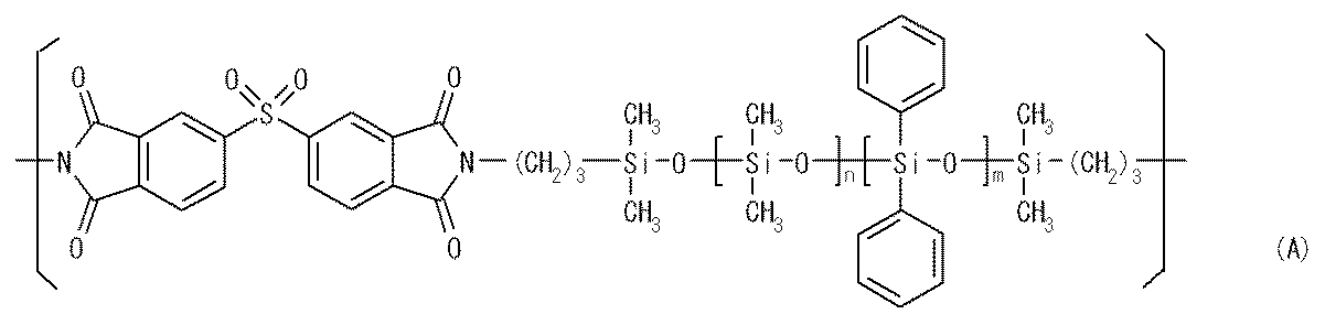
- シロキサン残基含有ポリイミドのシロキサン残基が、式(1)のシロキサンジアミン由来である請求項2記載のシールドフィルム。
(式中、nは1~30の整数であり、mは0~20の整数である。)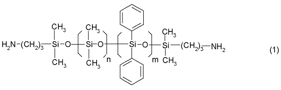
- バインダー樹脂が、更に、エポキシ樹脂とエポキシ樹脂用硬化剤とを含有する請求項1~3のいずれかに記載のシールドフィルム。
- バインダー樹脂が、シロキサン残基含有ポリイミド100質量部に対し、エポキシ樹脂を65~230質量部、エポキシ樹脂用硬化剤を45~150質量部の割合で含有する請求項4記載のシールドフィルム。
- エポキシ樹脂用硬化剤が、酸無水物系硬化剤である請求項4又は5記載のシールドフィルム。
- シロキサン残基含有ポリイミドが、少なくともテトラカルボン酸二無水物とシロキサンジアミンとを反応させてシロキサンポリイミド樹脂を製造する方法であって、以下の工程(a)~(c):
(a)溶媒中で第1のテトラカルボン酸二無水物とシロキサンジアミンとを還流条件下でイミド化反応させて酸無水物末端又はアミン末端シロキサンイミドオリゴマーを含む反応混合物を得る工程
(b)工程(a)で得られた反応混合物を減圧濃縮して反応濃縮物を得る工程
(c)工程(b)で得られた反応濃縮物に、溶媒とシロキサン非含有ジアミンとを添加し、シロキサン非含有ジアミンと反応濃縮物中の酸無水物末端シロキサンイミドオリゴマーとをイミド化反応させ、又は溶媒と第2のテトラカルボン酸二無水物とを添加し、第2のテトラカルボン酸二無水物と反応濃縮物中のアミン末端シロキサンイミドオリゴマーとをイミド化反応させ、それによりシロキサンポリイミド樹脂を得る工程
を有する製造方法により製造されたものである請求項1記載のシールドフィルム。 - 請求項1記載のシールドフィルムの製造方法であって、以下の工程:
第1の剥離基材に保護層形成用塗料を塗布し、乾燥することにより保護層を形成する工程;
第2の剥離基材に、シロキサン残基含有ポリイミドを含有するバインダー樹脂と導電性フィラーとを含有する導電性接着層形成用塗料を塗布し、乾燥することにより導電性接着層を形成する工程;
保護層と導電性接着層とを互いに貼り合わせることによりシールドフィルムを形成する工程
を有することを特徴とする製造方法。 - 保護層形成用塗料が、シロキサン残基含有ポリイミドを含有する請求項8記載の製造方法。
- グランド配線が形成された配線板上に、グランド配線と導通するように、請求項1~7のいずれかに記載のシールドフィルムが、その導電性接着層により積層されていることを特徴とするシールド配線板。
Applications Claiming Priority (4)
| Application Number | Priority Date | Filing Date | Title |
|---|---|---|---|
| JP2008-316554 | 2008-12-12 | ||
| JP2008316554 | 2008-12-12 | ||
| JP2009-009671 | 2009-01-20 | ||
| JP2009009671A JP2010161324A (ja) | 2008-12-12 | 2009-01-20 | シールドフィルム及びシールド配線板 |
Publications (1)
| Publication Number | Publication Date |
|---|---|
| WO2010067485A1 true WO2010067485A1 (ja) | 2010-06-17 |
Family
ID=42242484
Family Applications (1)
| Application Number | Title | Priority Date | Filing Date |
|---|---|---|---|
| PCT/JP2009/003677 Ceased WO2010067485A1 (ja) | 2008-12-12 | 2009-08-03 | シールドフィルム及びシールド配線板 |
Country Status (3)
| Country | Link |
|---|---|
| JP (1) | JP2010161324A (ja) |
| TW (1) | TW201022029A (ja) |
| WO (1) | WO2010067485A1 (ja) |
Cited By (4)
| Publication number | Priority date | Publication date | Assignee | Title |
|---|---|---|---|---|
| JP2012015311A (ja) * | 2010-06-30 | 2012-01-19 | Sony Chemical & Information Device Corp | シールドフィルム及びシールド配線板 |
| US9236169B2 (en) | 2012-11-21 | 2016-01-12 | Industrial Technology Research Institute | Electromagnetic wave shielding structure and method for fabricating the same |
| WO2020241523A1 (ja) * | 2019-05-24 | 2020-12-03 | 旭化成株式会社 | ポリイミド前駆体及びポリイミド樹脂組成物 |
| CN114573810A (zh) * | 2020-11-30 | 2022-06-03 | 旭化成株式会社 | 聚酰亚胺前体及聚酰亚胺树脂组合物 |
Families Citing this family (3)
| Publication number | Priority date | Publication date | Assignee | Title |
|---|---|---|---|---|
| WO2014137162A1 (ko) * | 2013-03-05 | 2014-09-12 | 주식회사 잉크테크 | 전자파 차폐 필름 및 그 제조방법 |
| KR101321511B1 (ko) * | 2013-05-21 | 2013-10-28 | (주)켐스 | 커버레이 일체형 전자파 흡수시트의 제조방법 및 그에 의한 커버레이 일체형 전자파 흡수시트 |
| JP6155339B2 (ja) * | 2013-08-29 | 2017-06-28 | 住友理工株式会社 | 柔軟導電材料およびトランスデューサ |
Citations (8)
| Publication number | Priority date | Publication date | Assignee | Title |
|---|---|---|---|---|
| JPH0415225A (ja) * | 1990-05-10 | 1992-01-20 | Sumitomo Bakelite Co Ltd | 溶剤可溶性ポリイミドシロキサンオリゴマー及びそれを含有する組成物 |
| JPH04222889A (ja) * | 1990-12-25 | 1992-08-12 | Sumitomo Bakelite Co Ltd | 導電性樹脂ペースト |
| JPH0525453A (ja) * | 1990-11-30 | 1993-02-02 | Ube Ind Ltd | 耐熱性樹脂接着剤 |
| JPH1145618A (ja) * | 1997-06-18 | 1999-02-16 | Internatl Business Mach Corp <Ibm> | 導電ペースト構造およびその製造方法 |
| JP2002069419A (ja) * | 2000-08-30 | 2002-03-08 | Ube Ind Ltd | 耐熱性接着剤および積層物 |
| JP2004273577A (ja) * | 2003-03-06 | 2004-09-30 | Sumitomo Electric Printed Circuit Inc | シールドフィルムおよびその製造方法 |
| JP2005109160A (ja) * | 2003-09-30 | 2005-04-21 | Tokai Rubber Ind Ltd | 電磁波シールドテープおよびそれを用いたシールドフラットケーブル |
| JP2006007589A (ja) * | 2004-06-25 | 2006-01-12 | Sumitomo Electric Printed Circuit Inc | 金属膜及び接着剤層を有する積層フィルム及びその製造方法 |
-
2009
- 2009-01-20 JP JP2009009671A patent/JP2010161324A/ja active Pending
- 2009-08-03 WO PCT/JP2009/003677 patent/WO2010067485A1/ja not_active Ceased
- 2009-08-13 TW TW098127194A patent/TW201022029A/zh unknown
Patent Citations (8)
| Publication number | Priority date | Publication date | Assignee | Title |
|---|---|---|---|---|
| JPH0415225A (ja) * | 1990-05-10 | 1992-01-20 | Sumitomo Bakelite Co Ltd | 溶剤可溶性ポリイミドシロキサンオリゴマー及びそれを含有する組成物 |
| JPH0525453A (ja) * | 1990-11-30 | 1993-02-02 | Ube Ind Ltd | 耐熱性樹脂接着剤 |
| JPH04222889A (ja) * | 1990-12-25 | 1992-08-12 | Sumitomo Bakelite Co Ltd | 導電性樹脂ペースト |
| JPH1145618A (ja) * | 1997-06-18 | 1999-02-16 | Internatl Business Mach Corp <Ibm> | 導電ペースト構造およびその製造方法 |
| JP2002069419A (ja) * | 2000-08-30 | 2002-03-08 | Ube Ind Ltd | 耐熱性接着剤および積層物 |
| JP2004273577A (ja) * | 2003-03-06 | 2004-09-30 | Sumitomo Electric Printed Circuit Inc | シールドフィルムおよびその製造方法 |
| JP2005109160A (ja) * | 2003-09-30 | 2005-04-21 | Tokai Rubber Ind Ltd | 電磁波シールドテープおよびそれを用いたシールドフラットケーブル |
| JP2006007589A (ja) * | 2004-06-25 | 2006-01-12 | Sumitomo Electric Printed Circuit Inc | 金属膜及び接着剤層を有する積層フィルム及びその製造方法 |
Cited By (8)
| Publication number | Priority date | Publication date | Assignee | Title |
|---|---|---|---|---|
| JP2012015311A (ja) * | 2010-06-30 | 2012-01-19 | Sony Chemical & Information Device Corp | シールドフィルム及びシールド配線板 |
| US9236169B2 (en) | 2012-11-21 | 2016-01-12 | Industrial Technology Research Institute | Electromagnetic wave shielding structure and method for fabricating the same |
| WO2020241523A1 (ja) * | 2019-05-24 | 2020-12-03 | 旭化成株式会社 | ポリイミド前駆体及びポリイミド樹脂組成物 |
| JPWO2020241523A1 (ja) * | 2019-05-24 | 2021-12-09 | 旭化成株式会社 | ポリイミド前駆体及びポリイミド樹脂組成物 |
| CN113874419A (zh) * | 2019-05-24 | 2021-12-31 | 旭化成株式会社 | 聚酰亚胺前体及聚酰亚胺树脂组合物 |
| JP7300504B2 (ja) | 2019-05-24 | 2023-06-29 | 旭化成株式会社 | ポリイミド前駆体及びポリイミド樹脂組成物 |
| CN113874419B (zh) * | 2019-05-24 | 2024-01-09 | 旭化成株式会社 | 聚酰亚胺前体及聚酰亚胺树脂组合物 |
| CN114573810A (zh) * | 2020-11-30 | 2022-06-03 | 旭化成株式会社 | 聚酰亚胺前体及聚酰亚胺树脂组合物 |
Also Published As
| Publication number | Publication date |
|---|---|
| TW201022029A (en) | 2010-06-16 |
| JP2010161324A (ja) | 2010-07-22 |
Similar Documents
| Publication | Publication Date | Title |
|---|---|---|
| JP5533354B2 (ja) | シールドフィルム及びシールド配線板 | |
| TWI743345B (zh) | 聚醯亞胺、黏著劑、薄膜狀黏著材料、黏著層、黏著片、附有樹脂之銅箔、覆銅積層板、印刷線路板、以及多層線路板及其製造方法 | |
| KR102863271B1 (ko) | 금속 피복 적층판, 회로 기판, 다층 회로 기판 및 그의 제조 방법 | |
| CN108690194B (zh) | 聚酰亚胺、胶粘剂、胶粘材料、胶粘层、胶粘片、铜箔、覆铜层叠板、布线板及制造方法 | |
| CN108690552B (zh) | 胶粘剂、胶粘材料、胶粘层、胶粘片、铜箔、覆铜层叠板、布线板及制造方法 | |
| JP3136942B2 (ja) | ポリイミドシロキサンの組成物 | |
| WO1994014911A1 (fr) | Film adhesif thermoresistant pour plaque de circuits imprimes et procede de realisation de ce film | |
| KR20110084526A (ko) | 프린트 배선판용 수지 조성물 | |
| TWI882013B (zh) | 熱硬化性樹脂組成物、熱硬化性樹脂薄片、電子零件、及電子裝置 | |
| WO2010067485A1 (ja) | シールドフィルム及びシールド配線板 | |
| JP3539633B2 (ja) | アルコキシ基含有シラン変性ポリアミック酸樹脂組成物およびポリイミド−シリカハイブリッド硬化物 | |
| JP3243963B2 (ja) | ポリイミドシロキサン組成物 | |
| JP5019874B2 (ja) | 熱硬化性樹脂組成物、及びそれを用いてなる積層体、回路基板 | |
| KR20040090387A (ko) | 열경화성 수지 조성물, 이를 이용한 적층체 및 회로 기판 | |
| JP2004035650A (ja) | ポリイミド樹脂、これを含有する樹脂組成物、電子部品用被覆材料及び電子部品用接着剤 | |
| JP4426774B2 (ja) | 熱硬化性樹脂組成物、及びそれを用いてなる積層体、回路基板 | |
| US6468639B2 (en) | Single-application polyimidosiloxane-based coating material and cured film | |
| JP4099769B2 (ja) | メトキシシリル基含有シラン変性ポリイミドシロキサン樹脂の製造法、当該樹脂、当該樹脂組成物、硬化膜および金属箔積層体 | |
| JP3074661B2 (ja) | ポリイミドシロキサン組成物 | |
| JP3577986B2 (ja) | カバ−レイ用接着シ−トおよび回路基板 | |
| TWI701272B (zh) | 樹脂組成物、黏著劑、薄膜狀黏著材料、黏著薄片、多層線路板、附有樹脂之銅箔、覆銅積層板、印刷線路板 | |
| JP4749606B2 (ja) | エポキシ基含有ポリイミド共重合体及びその硬化物 | |
| JPH10195402A (ja) | 耐熱性樹脂接着剤シ−トおよび基板 | |
| JPH09118808A (ja) | ポリイミドシロキサンの組成物 | |
| JP3111441B2 (ja) | プリント配線板用基板 |
Legal Events
| Date | Code | Title | Description |
|---|---|---|---|
| 121 | Ep: the epo has been informed by wipo that ep was designated in this application |
Ref document number: 09831594 Country of ref document: EP Kind code of ref document: A1 |
|
| DPE1 | Request for preliminary examination filed after expiration of 19th month from priority date (pct application filed from 20040101) | ||
| NENP | Non-entry into the national phase |
Ref country code: DE |
|
| 122 | Ep: pct application non-entry in european phase |
Ref document number: 09831594 Country of ref document: EP Kind code of ref document: A1 |