WO2010064467A1 - 多層プリント配線板、及び、多層プリント配線板の製造方法 - Google Patents
多層プリント配線板、及び、多層プリント配線板の製造方法 Download PDFInfo
- Publication number
- WO2010064467A1 WO2010064467A1 PCT/JP2009/062683 JP2009062683W WO2010064467A1 WO 2010064467 A1 WO2010064467 A1 WO 2010064467A1 JP 2009062683 W JP2009062683 W JP 2009062683W WO 2010064467 A1 WO2010064467 A1 WO 2010064467A1
- Authority
- WO
- WIPO (PCT)
- Prior art keywords
- printed wiring
- wiring board
- multilayer printed
- conductor
- recess
- Prior art date
- Legal status (The legal status is an assumption and is not a legal conclusion. Google has not performed a legal analysis and makes no representation as to the accuracy of the status listed.)
- Ceased
Links
Images











Classifications
-
- H—ELECTRICITY
- H05—ELECTRIC TECHNIQUES NOT OTHERWISE PROVIDED FOR
- H05K—PRINTED CIRCUITS; CASINGS OR CONSTRUCTIONAL DETAILS OF ELECTRIC APPARATUS; MANUFACTURE OF ASSEMBLAGES OF ELECTRICAL COMPONENTS
- H05K3/00—Apparatus or processes for manufacturing printed circuits
- H05K3/46—Manufacturing multilayer circuits
- H05K3/4644—Manufacturing multilayer circuits by building the multilayer layer by layer, i.e. build-up multilayer circuits
- H05K3/465—Manufacturing multilayer circuits by building the multilayer layer by layer, i.e. build-up multilayer circuits by applying an insulating layer having channels for the next circuit layer
-
- H—ELECTRICITY
- H10—SEMICONDUCTOR DEVICES; ELECTRIC SOLID-STATE DEVICES NOT OTHERWISE PROVIDED FOR
- H10W—GENERIC PACKAGES, INTERCONNECTIONS, CONNECTORS OR OTHER CONSTRUCTIONAL DETAILS OF DEVICES COVERED BY CLASS H10
- H10W70/00—Package substrates; Interposers; Redistribution layers [RDL]
- H10W70/60—Insulating or insulated package substrates; Interposers; Redistribution layers
- H10W70/62—Insulating or insulated package substrates; Interposers; Redistribution layers characterised by their interconnections
- H10W70/63—Vias, e.g. via plugs
- H10W70/635—Through-vias
-
- H—ELECTRICITY
- H10—SEMICONDUCTOR DEVICES; ELECTRIC SOLID-STATE DEVICES NOT OTHERWISE PROVIDED FOR
- H10W—GENERIC PACKAGES, INTERCONNECTIONS, CONNECTORS OR OTHER CONSTRUCTIONAL DETAILS OF DEVICES COVERED BY CLASS H10
- H10W70/00—Package substrates; Interposers; Redistribution layers [RDL]
- H10W70/60—Insulating or insulated package substrates; Interposers; Redistribution layers
- H10W70/62—Insulating or insulated package substrates; Interposers; Redistribution layers characterised by their interconnections
- H10W70/65—Shapes or dispositions of interconnections
-
- H—ELECTRICITY
- H10—SEMICONDUCTOR DEVICES; ELECTRIC SOLID-STATE DEVICES NOT OTHERWISE PROVIDED FOR
- H10W—GENERIC PACKAGES, INTERCONNECTIONS, CONNECTORS OR OTHER CONSTRUCTIONAL DETAILS OF DEVICES COVERED BY CLASS H10
- H10W70/00—Package substrates; Interposers; Redistribution layers [RDL]
- H10W70/60—Insulating or insulated package substrates; Interposers; Redistribution layers
- H10W70/62—Insulating or insulated package substrates; Interposers; Redistribution layers characterised by their interconnections
- H10W70/65—Shapes or dispositions of interconnections
- H10W70/6565—Shapes or dispositions of interconnections recessed into the surface of the package substrates, interposers, or redistribution layers
-
- H—ELECTRICITY
- H10—SEMICONDUCTOR DEVICES; ELECTRIC SOLID-STATE DEVICES NOT OTHERWISE PROVIDED FOR
- H10W—GENERIC PACKAGES, INTERCONNECTIONS, CONNECTORS OR OTHER CONSTRUCTIONAL DETAILS OF DEVICES COVERED BY CLASS H10
- H10W70/00—Package substrates; Interposers; Redistribution layers [RDL]
- H10W70/60—Insulating or insulated package substrates; Interposers; Redistribution layers
- H10W70/67—Insulating or insulated package substrates; Interposers; Redistribution layers characterised by their insulating layers or insulating parts
- H10W70/68—Shapes or dispositions thereof
- H10W70/685—Shapes or dispositions thereof comprising multiple insulating layers
-
- H—ELECTRICITY
- H05—ELECTRIC TECHNIQUES NOT OTHERWISE PROVIDED FOR
- H05K—PRINTED CIRCUITS; CASINGS OR CONSTRUCTIONAL DETAILS OF ELECTRIC APPARATUS; MANUFACTURE OF ASSEMBLAGES OF ELECTRICAL COMPONENTS
- H05K2201/00—Indexing scheme relating to printed circuits covered by H05K1/00
- H05K2201/03—Conductive materials
- H05K2201/0332—Structure of the conductor
- H05K2201/0364—Conductor shape
- H05K2201/0373—Conductors having a fine structure, e.g. providing a plurality of contact points with a structured tool
-
- H—ELECTRICITY
- H05—ELECTRIC TECHNIQUES NOT OTHERWISE PROVIDED FOR
- H05K—PRINTED CIRCUITS; CASINGS OR CONSTRUCTIONAL DETAILS OF ELECTRIC APPARATUS; MANUFACTURE OF ASSEMBLAGES OF ELECTRICAL COMPONENTS
- H05K2201/00—Indexing scheme relating to printed circuits covered by H05K1/00
- H05K2201/09—Shape and layout
- H05K2201/09209—Shape and layout details of conductors
- H05K2201/09372—Pads and lands
- H05K2201/0949—Pad close to a hole, not surrounding the hole
-
- H—ELECTRICITY
- H05—ELECTRIC TECHNIQUES NOT OTHERWISE PROVIDED FOR
- H05K—PRINTED CIRCUITS; CASINGS OR CONSTRUCTIONAL DETAILS OF ELECTRIC APPARATUS; MANUFACTURE OF ASSEMBLAGES OF ELECTRICAL COMPONENTS
- H05K2201/00—Indexing scheme relating to printed circuits covered by H05K1/00
- H05K2201/09—Shape and layout
- H05K2201/09209—Shape and layout details of conductors
- H05K2201/09654—Shape and layout details of conductors covering at least two types of conductors provided for in H05K2201/09218 - H05K2201/095
- H05K2201/09736—Varying thickness of a single conductor; Conductors in the same plane having different thicknesses
-
- H—ELECTRICITY
- H05—ELECTRIC TECHNIQUES NOT OTHERWISE PROVIDED FOR
- H05K—PRINTED CIRCUITS; CASINGS OR CONSTRUCTIONAL DETAILS OF ELECTRIC APPARATUS; MANUFACTURE OF ASSEMBLAGES OF ELECTRICAL COMPONENTS
- H05K2201/00—Indexing scheme relating to printed circuits covered by H05K1/00
- H05K2201/10—Details of components or other objects attached to or integrated in a printed circuit board
- H05K2201/10613—Details of electrical connections of non-printed components, e.g. special leads
- H05K2201/10621—Components characterised by their electrical contacts
- H05K2201/10674—Flip chip
-
- H—ELECTRICITY
- H10—SEMICONDUCTOR DEVICES; ELECTRIC SOLID-STATE DEVICES NOT OTHERWISE PROVIDED FOR
- H10P—GENERIC PROCESSES OR APPARATUS FOR THE MANUFACTURE OR TREATMENT OF DEVICES COVERED BY CLASS H10
- H10P72/00—Handling or holding of wafers, substrates or devices during manufacture or treatment thereof
- H10P72/70—Handling or holding of wafers, substrates or devices during manufacture or treatment thereof for supporting or gripping
- H10P72/74—Handling or holding of wafers, substrates or devices during manufacture or treatment thereof for supporting or gripping using temporarily an auxiliary support
- H10P72/7424—Handling or holding of wafers, substrates or devices during manufacture or treatment thereof for supporting or gripping using temporarily an auxiliary support used as a support during the manufacture of self-supporting substrates
-
- H—ELECTRICITY
- H10—SEMICONDUCTOR DEVICES; ELECTRIC SOLID-STATE DEVICES NOT OTHERWISE PROVIDED FOR
- H10W—GENERIC PACKAGES, INTERCONNECTIONS, CONNECTORS OR OTHER CONSTRUCTIONAL DETAILS OF DEVICES COVERED BY CLASS H10
- H10W70/00—Package substrates; Interposers; Redistribution layers [RDL]
- H10W70/60—Insulating or insulated package substrates; Interposers; Redistribution layers
- H10W70/62—Insulating or insulated package substrates; Interposers; Redistribution layers characterised by their interconnections
- H10W70/65—Shapes or dispositions of interconnections
- H10W70/654—Top-view layouts
- H10W70/655—Fan-out layouts
-
- H—ELECTRICITY
- H10—SEMICONDUCTOR DEVICES; ELECTRIC SOLID-STATE DEVICES NOT OTHERWISE PROVIDED FOR
- H10W—GENERIC PACKAGES, INTERCONNECTIONS, CONNECTORS OR OTHER CONSTRUCTIONAL DETAILS OF DEVICES COVERED BY CLASS H10
- H10W72/00—Interconnections or connectors in packages
- H10W72/071—Connecting or disconnecting
- H10W72/072—Connecting or disconnecting of bump connectors
- H10W72/07251—Connecting or disconnecting of bump connectors characterised by changes in properties of the bump connectors during connecting
-
- H—ELECTRICITY
- H10—SEMICONDUCTOR DEVICES; ELECTRIC SOLID-STATE DEVICES NOT OTHERWISE PROVIDED FOR
- H10W—GENERIC PACKAGES, INTERCONNECTIONS, CONNECTORS OR OTHER CONSTRUCTIONAL DETAILS OF DEVICES COVERED BY CLASS H10
- H10W72/00—Interconnections or connectors in packages
- H10W72/20—Bump connectors, e.g. solder bumps or copper pillars; Dummy bumps; Thermal bumps
-
- H—ELECTRICITY
- H10—SEMICONDUCTOR DEVICES; ELECTRIC SOLID-STATE DEVICES NOT OTHERWISE PROVIDED FOR
- H10W—GENERIC PACKAGES, INTERCONNECTIONS, CONNECTORS OR OTHER CONSTRUCTIONAL DETAILS OF DEVICES COVERED BY CLASS H10
- H10W72/00—Interconnections or connectors in packages
- H10W72/90—Bond pads, in general
-
- H—ELECTRICITY
- H10—SEMICONDUCTOR DEVICES; ELECTRIC SOLID-STATE DEVICES NOT OTHERWISE PROVIDED FOR
- H10W—GENERIC PACKAGES, INTERCONNECTIONS, CONNECTORS OR OTHER CONSTRUCTIONAL DETAILS OF DEVICES COVERED BY CLASS H10
- H10W72/00—Interconnections or connectors in packages
- H10W72/90—Bond pads, in general
- H10W72/921—Structures or relative sizes of bond pads
- H10W72/923—Bond pads having multiple stacked layers
-
- H—ELECTRICITY
- H10—SEMICONDUCTOR DEVICES; ELECTRIC SOLID-STATE DEVICES NOT OTHERWISE PROVIDED FOR
- H10W—GENERIC PACKAGES, INTERCONNECTIONS, CONNECTORS OR OTHER CONSTRUCTIONAL DETAILS OF DEVICES COVERED BY CLASS H10
- H10W72/00—Interconnections or connectors in packages
- H10W72/90—Bond pads, in general
- H10W72/941—Dispositions of bond pads
- H10W72/9415—Dispositions of bond pads relative to the surface, e.g. recessed, protruding
-
- H—ELECTRICITY
- H10—SEMICONDUCTOR DEVICES; ELECTRIC SOLID-STATE DEVICES NOT OTHERWISE PROVIDED FOR
- H10W—GENERIC PACKAGES, INTERCONNECTIONS, CONNECTORS OR OTHER CONSTRUCTIONAL DETAILS OF DEVICES COVERED BY CLASS H10
- H10W90/00—Package configurations
- H10W90/701—Package configurations characterised by the relative positions of pads or connectors relative to package parts
- H10W90/721—Package configurations characterised by the relative positions of pads or connectors relative to package parts of bump connectors
- H10W90/724—Package configurations characterised by the relative positions of pads or connectors relative to package parts of bump connectors between a chip and a stacked insulating package substrate, interposer or RDL
-
- Y—GENERAL TAGGING OF NEW TECHNOLOGICAL DEVELOPMENTS; GENERAL TAGGING OF CROSS-SECTIONAL TECHNOLOGIES SPANNING OVER SEVERAL SECTIONS OF THE IPC; TECHNICAL SUBJECTS COVERED BY FORMER USPC CROSS-REFERENCE ART COLLECTIONS [XRACs] AND DIGESTS
- Y10—TECHNICAL SUBJECTS COVERED BY FORMER USPC
- Y10T—TECHNICAL SUBJECTS COVERED BY FORMER US CLASSIFICATION
- Y10T29/00—Metal working
- Y10T29/49—Method of mechanical manufacture
- Y10T29/49002—Electrical device making
- Y10T29/49117—Conductor or circuit manufacturing
- Y10T29/49124—On flat or curved insulated base, e.g., printed circuit, etc.
- Y10T29/49126—Assembling bases
-
- Y—GENERAL TAGGING OF NEW TECHNOLOGICAL DEVELOPMENTS; GENERAL TAGGING OF CROSS-SECTIONAL TECHNOLOGIES SPANNING OVER SEVERAL SECTIONS OF THE IPC; TECHNICAL SUBJECTS COVERED BY FORMER USPC CROSS-REFERENCE ART COLLECTIONS [XRACs] AND DIGESTS
- Y10—TECHNICAL SUBJECTS COVERED BY FORMER USPC
- Y10T—TECHNICAL SUBJECTS COVERED BY FORMER US CLASSIFICATION
- Y10T29/00—Metal working
- Y10T29/49—Method of mechanical manufacture
- Y10T29/49002—Electrical device making
- Y10T29/49117—Conductor or circuit manufacturing
- Y10T29/49124—On flat or curved insulated base, e.g., printed circuit, etc.
- Y10T29/49128—Assembling formed circuit to base
-
- Y—GENERAL TAGGING OF NEW TECHNOLOGICAL DEVELOPMENTS; GENERAL TAGGING OF CROSS-SECTIONAL TECHNOLOGIES SPANNING OVER SEVERAL SECTIONS OF THE IPC; TECHNICAL SUBJECTS COVERED BY FORMER USPC CROSS-REFERENCE ART COLLECTIONS [XRACs] AND DIGESTS
- Y10—TECHNICAL SUBJECTS COVERED BY FORMER USPC
- Y10T—TECHNICAL SUBJECTS COVERED BY FORMER US CLASSIFICATION
- Y10T29/00—Metal working
- Y10T29/49—Method of mechanical manufacture
- Y10T29/49002—Electrical device making
- Y10T29/49117—Conductor or circuit manufacturing
- Y10T29/49124—On flat or curved insulated base, e.g., printed circuit, etc.
- Y10T29/4913—Assembling to base an electrical component, e.g., capacitor, etc.
-
- Y—GENERAL TAGGING OF NEW TECHNOLOGICAL DEVELOPMENTS; GENERAL TAGGING OF CROSS-SECTIONAL TECHNOLOGIES SPANNING OVER SEVERAL SECTIONS OF THE IPC; TECHNICAL SUBJECTS COVERED BY FORMER USPC CROSS-REFERENCE ART COLLECTIONS [XRACs] AND DIGESTS
- Y10—TECHNICAL SUBJECTS COVERED BY FORMER USPC
- Y10T—TECHNICAL SUBJECTS COVERED BY FORMER US CLASSIFICATION
- Y10T29/00—Metal working
- Y10T29/49—Method of mechanical manufacture
- Y10T29/49002—Electrical device making
- Y10T29/49117—Conductor or circuit manufacturing
- Y10T29/49124—On flat or curved insulated base, e.g., printed circuit, etc.
- Y10T29/49155—Manufacturing circuit on or in base
-
- Y—GENERAL TAGGING OF NEW TECHNOLOGICAL DEVELOPMENTS; GENERAL TAGGING OF CROSS-SECTIONAL TECHNOLOGIES SPANNING OVER SEVERAL SECTIONS OF THE IPC; TECHNICAL SUBJECTS COVERED BY FORMER USPC CROSS-REFERENCE ART COLLECTIONS [XRACs] AND DIGESTS
- Y10—TECHNICAL SUBJECTS COVERED BY FORMER USPC
- Y10T—TECHNICAL SUBJECTS COVERED BY FORMER US CLASSIFICATION
- Y10T29/00—Metal working
- Y10T29/49—Method of mechanical manufacture
- Y10T29/49002—Electrical device making
- Y10T29/49117—Conductor or circuit manufacturing
- Y10T29/49124—On flat or curved insulated base, e.g., printed circuit, etc.
- Y10T29/49155—Manufacturing circuit on or in base
- Y10T29/49156—Manufacturing circuit on or in base with selective destruction of conductive paths
-
- Y—GENERAL TAGGING OF NEW TECHNOLOGICAL DEVELOPMENTS; GENERAL TAGGING OF CROSS-SECTIONAL TECHNOLOGIES SPANNING OVER SEVERAL SECTIONS OF THE IPC; TECHNICAL SUBJECTS COVERED BY FORMER USPC CROSS-REFERENCE ART COLLECTIONS [XRACs] AND DIGESTS
- Y10—TECHNICAL SUBJECTS COVERED BY FORMER USPC
- Y10T—TECHNICAL SUBJECTS COVERED BY FORMER US CLASSIFICATION
- Y10T29/00—Metal working
- Y10T29/49—Method of mechanical manufacture
- Y10T29/49002—Electrical device making
- Y10T29/49117—Conductor or circuit manufacturing
- Y10T29/49124—On flat or curved insulated base, e.g., printed circuit, etc.
- Y10T29/49155—Manufacturing circuit on or in base
- Y10T29/49165—Manufacturing circuit on or in base by forming conductive walled aperture in base
Definitions
- the present invention relates to a build-up type multilayer printed wiring board and a method for manufacturing the multilayer printed wiring board, and more particularly to a multilayer printed wiring board having a plane conductor and a method for manufacturing the multilayer printed wiring board.
- a printed wiring board constituting a package substrate on which electronic components such as an IC chip are mounted is required to have a fine pitch circuit configuration as the performance of the IC chip increases.
- circuit formation by a laser as shown in Patent Document 1 is proposed instead of circuit formation by a conventional semi-additive method.
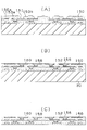
- the interlayer resin insulating layer 350 shown in FIG. 28A is irradiated with a laser by a laser forming recess 353b, a via conductor forming opening 351, and a plane.
- a recess 353a for forming a conductor is formed. Then, as shown in FIG.
- an electroless plating film 352 and an electrolytic plating film 356 are deposited in a recess 353b for forming a circuit, an opening 351 for forming a via conductor, and a recess 353a for forming a plain conductor, and a conductor circuit 358 is formed.
- the via conductor 360 and the plain conductor 359 are formed.
- the normal printed wiring board is set so that the copper volume is almost the same on the front surface side and the back surface side so that, for example, it is difficult for warpage to occur in a heat cycle in which the IC chip generates heat and then returns to room temperature. ing. For this reason, when a dent arises in wiring (plane conductor), since the volume becomes smaller than a design value, deviation arises in the volume adjustment of copper in the front and back. This may cause the printed wiring board to warp while repeating the heat cycle in which the IC chip generates heat and then returns to room temperature.
- the present invention has been made to solve the above-described problems, and the object of the present invention is to provide a method for manufacturing a multilayer printed wiring board that can form a plane conductor flat, and a flat multilayer printed wiring having a flat conductor. To provide a board.
- a method for producing a multilayer printed wiring board comprises: Forming a first conductor circuit on or in the first resin insulation; Forming a second resin insulation on the first resin insulation and the first conductor circuit; Forming a first recess for a second conductor circuit on the first surface side of the second resin insulation; Forming a pattern for a plain conductor composed of a second concave portion and a convex portion on the first surface side of the second resin insulating material; The first and second recesses are filled with a conductive material to form a second conductor circuit and a plain conductor.
- the multilayer printed wiring board according to claim 13 includes a first resin insulating material, a first conductor circuit formed on or in the first resin insulating material, the first resin insulating material, A second resin insulating material formed on the first conductor circuit, having a first recess for the second conductor circuit and a pattern for the plain conductor on the first surface side, and a second resin insulating material formed in the first recess.
- One technical feature is that one surface is located on substantially the same plane.
- the convex portion is formed in the concave portion for forming the plain conductor of the upper insulating material, when the conductive material is plated and filled in the concave portion for forming the plain conductor, The conductive material is uniformly deposited not only from the side wall of the concave portion but also from the side wall of the convex portion. For this reason, a plane conductor can be formed flat.
- the surface of the plain conductor and the surface (first surface) of the second resin insulating material are located on substantially the same plane. Thereby, the planarization of the other resin insulating material formed on the plain conductor and the second resin insulating material is achieved.
- insulation interlayer insulation
- the volume of the metal part including the plane conductor can be controlled as designed, warpage of the multilayer printed wiring board can be suppressed in a heat cycle caused by heat generation of the IC chip, for example.
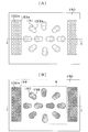
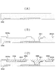
- FIG. 10A is a plan view of the multilayer printed wiring board showing the aa cross section of FIG. 6A
- FIG. 10B is the multilayer print showing the cc cross section of FIG. 6C.
- 11A is an enlarged view of the concave portion for forming the plain conductor in FIG. 6A
- FIG. 11B is an enlarged view of the plain conductor in FIG. 6C.
- FIG. 13A is an explanatory diagram of the arrangement of the convex portions in the first embodiment, and FIG.
- FIG. 13B is an explanatory diagram of the arrangement of the convex portions according to the first modification of the first embodiment. It is process drawing which shows the manufacturing method of the multilayer printed wiring board which concerns on the 2nd modification of 1st Example.
- 15A is a plan view of the multilayer printed wiring board showing the aa cross section of FIG. 14A
- FIG. 15B is the multilayer print showing the cc cross section of FIG. 14C. It is a top view of a wiring board.
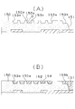
- FIG. 16A is an enlarged view of a plain conductor of a multilayer printed wiring board according to the third modification of the first embodiment
- FIG. 16B is a multilayer according to the fourth modification of the first embodiment. It is an enlarged view of the plain conductor of a printed wiring board.
- FIG. 24A is an image diagram in which the diameter (Post) f of the convex portions is taken on the horizontal axis and the interval (Space) d between the convex portions is taken on the vertical axis.
- FIG. 24B is a chart of test results. It is a photograph when the thickness of the plain conductor is set to 10 ⁇ m. It is a photograph when the thickness of the plain conductor is set to 15 ⁇ m. It is a photograph when the thickness of the plain conductor is set to 20 ⁇ m. It is process drawing which shows the manufacturing method of the plain conductor in a prior art.
- FIG. 29A is a photograph of the plain conductor formed by the conventional technique
- FIG. 29B is a photograph of the plain conductor formed by the manufacturing method of the first embodiment.
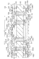
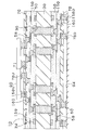
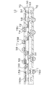
- FIGS. 8 shows a cross-sectional view of the multilayer printed wiring board 10
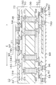
- FIG. 9 shows a state in which the IC chip 90 is attached to the multilayer printed wiring board 10 shown in FIG.
- FIG. 10B shows a bb cross section in FIG.
- a conductor circuit 34 is formed on the surface of the core substrate 30.
- the front surface and the back surface of the core substrate 30 are connected through a through hole 36.
- the through hole 36 includes a lid plating layer 36a constituting the through hole land and a side wall conductor layer 36b, and the side wall conductor layer 36b is filled with a resin filler 37. You may fill only with copper, without a resin filler.
- An upper surface side interlayer resin insulation layer 150 formed with a pad) and a lower surface side interlayer resin insulation layer 150 formed with a via hole 160 and a conductor circuit 158D (solder pad) are disposed.
- Conductor circuit 158U (solder pad) is provided in first recess 153b opened in first surface 150A of interlayer resin insulation layer 150.
- the surface of the conductor circuit 158U (solder pad) and the first surface 150A of the interlayer resin insulation layer 150 are located on substantially the same plane.
- the conductor circuit 158U (solder pad) is electrically connected to the underlying conductor circuit 58 via the via hole 160.
- a solder resist layer 70 is formed on the interlayer resin insulation layer 150.
- openings for exposing part of the conductor circuits 158U and 158D are formed.
- the part exposed from opening of conductor circuits 158U and 158D functions as a solder pad.
- the solder pads are arranged in the IC chip mounting area E located on the center side of the multilayer printed wiring board.
- An antioxidant film made of, for example, a Ni layer 72 and an Au layer 74 is formed on the solder pad, and a solder bump 78U is formed on the antioxidant film.
- the IC chip 90 is mounted on the multilayer printed wiring board via the solder bumps 78U.
- a pattern for forming a plain conductor composed of the second recess 153a and the protrusion 150a is formed (FIGS. 8 and 11A).
- the second recess 153a opens in the first surface of the interlayer resin insulation layer 150.
- the opening area of the second recess 153a is larger than the opening area of the first recess 153b. Is formed upward (first surface direction) from the surface of the interlayer resin insulation layer 150 that constitutes the bottom of the second concave portion, and shows a cross section of the convex portion 150a in FIG. Fig.
- FIG. 13 is a plan view showing the top surface of the convex portion 150a, and the convex portions 150a are arranged in a staggered manner so that the mutual distance d is uniform, as shown in Fig. 13A.
- the "distance d" here is Ri means the minimum value of the distance between the protrusions fit.
- a plain conductor 159 is formed in the second recess 153 a of the interlayer resin insulation layer 150.
- the surface of the plane conductor 159 is located on substantially the same plane as the surface (first surface) of the interlayer resin insulation layer 150.
- the plane conductor 159 may be used as a power source or ground conductor, or may be used as a dummy conductor.
- the multilayer printed wiring board 10 is connected to the daughter board 94 via solder bumps 78D.
- a starting material FIG. 1A
- the copper-clad laminate is drilled to form through holes 16 (FIG. 1B), and subjected to electroless plating and electrolytic plating to form sidewall conductor layers 36b of through holes 36. (FIG. 1C).
- a filler 37 containing copper particles having an average particle diameter of 10 ⁇ m (non-conductive hole-filling copper paste made by Tatsuta Electric Wire, trade name: DD paste) is filled into the through-hole 36 by screen printing and dried. And cured (FIG. 2A).
- a through-hole is filled by applying it by a printing method on a substrate on which a mask having an opening in the through-hole portion is placed, and then dried and cured.
- the filler 37 protruding from the through hole 36 is removed by belt sander polishing using # 600 belt polishing paper (manufactured by Sankyo Rikagaku), and further, buff polishing for removing scratches due to this belt sander polishing is performed.
- the surface of the substrate 30 is flattened (see FIG. 2B). In this way, the substrate 30 is obtained in which the side wall conductor layer 36b of the through hole 36 and the resin filler 37 are firmly adhered via the roughened layer 36 ⁇ .
- a palladium catalyst (manufactured by Atotech) is applied to the surface of the substrate 30 flattened in (3), and electroless copper plating is performed, thereby forming an electroless copper plating film 23 having a thickness of 0.6 ⁇ m. (See FIG. 2C).
- electrolytic copper plating is performed under the following conditions to form an electrolytic copper plating film 24 having a thickness of 15 ⁇ m, thickening a portion to become the conductor circuit 34, and a filler 37 filled in the through hole 36.
- a portion to be a cover plating layer (through-hole land) is formed (FIG. 2D).
- Sulfuric acid 180 g / l Copper sulfate 80 g / l Additive (product name: Kaparaside GL, manufactured by Atotech Japan) 1 ml / l
- Electrolytic plating conditions Current density 1A / dm 2 Time 70 minutes Temperature Room temperature
- a commercially available photosensitive dry film is pasted on both surfaces of the substrate 30 on which the conductor circuit and the lid plating layer are formed, and a mask is placed, exposed at 100 mJ / cm 2 , 0.8% sodium carbonate Is developed to form an etching resist 25 having a thickness of 15 ⁇ m (see FIG. 2E).
- the shape of the lid plating layer can be changed by adjusting the mask pattern.
- the portions of the plating films 23 and 24 and the copper foil 32 where the etching resist 25 is not formed are dissolved and removed with an etching solution containing cupric chloride as a main component.
- the lid plating layer 36a covering the independent conductor circuit 34 and the filler 37 is formed by peeling off with% KOH (see FIG. 3A).
- the surface of the lid plating layer 36a covering the conductor circuit 34 and the filler 37 is roughened to form a roughened surface 34 ⁇ (FIG. 3B).
- Such roughening can be performed by blackening using an alkali, etching using an appropriate etching solution, or the like.
- a microetching agent “CZ series” manufactured by MEC Co., Ltd.
- MEC Co., Ltd. MEC Co., Ltd.
- a resin film for an interlayer resin insulation layer (made by Ajinomoto Co., Inc .: trade name; ABF-45SH) 50 ⁇ that is slightly larger than the substrate is placed on the substrate, pressure 0.45 MPa, temperature 80 ° C., After temporarily crimping and cutting under conditions of a pressure bonding time of 10 seconds, an interlayer resin insulation layer 50 is formed by further bonding using a vacuum laminator device by the following method (FIG. 3C).
- the resin film for an interlayer resin insulation layer was subjected to main pressure bonding on a substrate under conditions of a degree of vacuum of 67 Pa, a pressure of 0.47 MPa, a temperature of 85 ° C., and a pressure bonding time of 60 seconds, and then thermally cured at 170 ° C. for 40 minutes.
- the substrate after the above treatment is immersed in a neutralization solution (manufactured by Shipley Co., Ltd.) and then washed with water. Further, by applying a palladium catalyst to the surface of the roughened substrate, catalyst nuclei were attached to the surface of the interlayer resin insulation layer and the inner wall surface of the via hole opening. That is, the substrate is immersed in a catalyst solution containing palladium chloride (PbCl 2 ) and stannous chloride (SnCl 2 ), and the catalyst is applied by depositing palladium metal.
- a neutralization solution manufactured by Shipley Co., Ltd.
- the substrate provided with the catalyst is immersed in an electroless copper plating aqueous solution (Sulcup PEA) manufactured by Uemura Kogyo Co., Ltd., and the entire surface is electroless copper having a thickness of 0.3 to 3.0 ⁇ m.
- a plating film was formed, and a substrate having an electroless copper plating film 52 formed on the surface of the interlayer resin insulating layer 50 including the inner wall of the via hole opening 51 was obtained (FIG. 4A).
- a commercially available photosensitive dry film is attached to the substrate on which the electroless copper plating film 52 is formed, a mask is placed, exposed at 110 mJ / cm 2 , and developed with a 0.8% aqueous sodium carbonate solution.
- a plating resist 54 having a thickness of 25 ⁇ m was provided (FIG. 4B).
- the substrate is washed with 50 ° C. water and degreased, washed with 25 ° C. water and further washed with sulfuric acid, and then subjected to electrolytic plating under the following conditions to form a plating resist 54 non-formed portion. Then, an electrolytic copper plating film 56 having a thickness of 15 ⁇ m is formed (FIG. 4C).
- the electroless plating film under the plating resist is etched and removed with a mixed solution of sulfuric acid and hydrogen peroxide to remove an independent conductor circuit. 58 and via hole 60 (FIG. 5A).
- the lower conductor circuit 58 had a thickness of 15 ⁇ m. However, the thickness of the lower conductor circuit may be between 5 and 25 ⁇ m.
- an interlayer resin insulation layer resin film (manufactured by Ajinomoto Co., Inc .: trade name; ABF-45SH) is placed on the substrate and affixed to the interlayer resin insulation layer 50.
- a resin insulating layer 150 is formed (FIG. 5B).
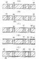
- Via holes 151 are formed in the interlayer resin insulation layer 150 with a CO2 gas laser in the same manner as in (10) above (FIG. 5C).
- a convex portion 150a is formed in the second concave portion 153a for forming a plain conductor.
- the convex part 150a is formed in a tapered shape toward the upper surface (first surface) as shown in FIG. Further, the upper surface of the convex portion 150 a is located on substantially the same plane as the first surface of the interlayer resin insulating layer 150. Further, the convex portions 150a are arranged in a staggered manner as shown in FIG.
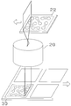
- the excimer laser is condensed by the projection lens 20 through the mask 22 on which the pattern is drawn and irradiated onto the substrate 30.
- the concave portion 153b for forming the conductor circuit and the pattern for forming the plain conductor are formed by fixing the projection lens 20 and relatively moving the mask 22 and the substrate 30.
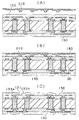
- an interlayer resin insulation layer including the inner walls of the via hole opening 151, the first recess 153b, and the second recess 153a is formed on the surface 150. This roughening process may be omitted.
- an electroless copper plating film 152 having a thickness of 0.3 to 3.0 ⁇ m is formed on the surface of the interlayer resin insulation layer 150.
- an electrolytic copper plating film 156 having a thickness of 15 ⁇ m is formed (FIG. 6B).
- the electrolytic copper plating is uniformly filled in the pattern for forming the plain conductor (the concave portion 153a). It becomes possible to make the surface of the electrolytic copper plating almost flat.
- the electrolytic copper plating film 156 is buffed until the upper surface (first surface) of the interlayer resin insulation layer 150 is exposed (FIG. 6C).
- An enlarged plane conductor 159 surrounded by an ellipse in FIG. 6C is shown in FIG. 11B, and a plan view of the interlayer resin insulating layer 150 in FIG. 6C is shown in FIG.
- buffing is performed here, instead of this, chemical mechanical polishing can be performed, or the surface layer of the electrolytic copper plating film 156 can be removed by light etching.
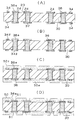
- solder resist composition 70 is applied to a thickness of 20 ⁇ m on both sides of the multilayer wiring board and performing a drying treatment at 70 ° C. for 20 minutes and at 70 ° C. for 30 minutes.
- a photomask having a thickness of 5 mm on which a pattern of the opening of the solder resist is drawn is brought into close contact with the solder resist layer 70, exposed to 1000 mJ / cm 2 of ultraviolet light, and developed with a DMTG solution to form an opening 71 having a diameter of 200 ⁇ m. (FIG. 7A).
- the solder resist layer is cured by heating at 80 ° C. for 1 hour, 100 ° C. for 1 hour, 120 ° C. for 1 hour, and 150 ° C. for 3 hours.
- a solder resist pattern layer having a thickness of 15 to 25 ⁇ m is formed.
- a 0.03 ⁇ m gold plating layer 74 is formed (FIG. 7B).
- a single layer of tin or a noble metal layer may be formed.
- solder paste containing tin-lead is printed on the opening 71 of the solder resist layer 70 on the surface on which the IC chip of the substrate is to be placed, and tin-lead is formed on the opening of the solder resist layer on the other surface.
- solder bumps solder bodies
- a multilayer printed wiring board having solder bumps 78U and 78D is manufactured (FIG. 8).
- the solder bumps 78U and 78D may be formed by reflowing at a predetermined temperature after mounting the solder balls on the solder pads.
- the composition of the solder ball is not particularly limited, and examples thereof include a solder ball made of tin-silver-copper.
- the IC chip 90 is attached via the solder bumps 78U. And it attaches to the daughter board 94 via the solder bump 78D (FIG. 9).
- a pattern for forming a plain conductor composed of the second concave portion 153a and the convex portion 150a is formed in the interlayer resin insulating layer 150.
- the electrolytic copper plating is deposited not only from the side wall 153s and the bottom surface 153c of the second concave portion 153a shown in FIG. 11A but also from the side surface 150s of the convex portion 150a. For this reason, as shown in the photograph of FIG. 29B, the surface of the copper plating filled in the second recess 153a can be formed flat. Polishing or etching the copper plating in this state makes it possible to flatten the surface of the plain conductor formed in the second recess 153a.
- the convex portion 150a is formed in a taper shape, the side wall 150s and the second concave portion 153a of the convex portion 150a shown in FIG. Voids are unlikely to remain at the corners C with the bottom surface 153c forming the. For this reason, the surface of the copper plating filled in the second recess 153a can be formed flat.
- the convex portions 150a are arranged in a staggered manner, and the distance d between the convex portions 150a is uniform as shown in FIG. Thereby, the amount of copper deposited from the side wall of the convex portion 150a becomes equal, and the plain conductor can be formed flat.
- the conductor circuit forming recess 153b and the plain conductor forming recess 153a are formed by laser. Since a fine concave portion can be formed by a laser, a fine pitch conductor circuit 158U can be formed.
- the copper for the copper pattern is formed in the pattern for forming the plane conductor.
- copper plating is deposited not only from the side wall of the pattern but also from the side wall of the convex portion 150a. For this reason, it becomes possible to form a plane conductor flat. Thereby, the planarization of the other resin insulating material formed on the plain conductor and the second resin insulating material is achieved.
- the surface of the solder resist layer can be flattened. According to this, for example, the surface of the ball alignment mask used when mounting the solder balls on the solder pads is also flattened, so that the solder balls can easily move on the ball alignment mask. As a result, the mounting efficiency of the solder balls is improved, and it becomes possible to mount one ball on the solder pad with a high probability.
- the height of the solder bumps protruding from the surface of the solder resist layer becomes uniform, and the mountability of the IC chip is improved. Further, since no excessive depression is formed on the surface of the plain conductor, the volume of the metal part including the plain conductor can be controlled as designed. As a result, it is possible to effectively suppress warping of the multilayer printed wiring board in a heat cycle caused by heat generation of the IC chip.
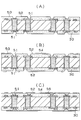
- FIG. 15A shows a plan view of the interlayer resin insulating layer 150 in FIG. FIG. 14A corresponds to the aa cross section of FIG.
- an electroless copper plating film 152 and an electrolytic copper plating film 156 are formed on the interlayer resin insulating layer 150 (FIG. 14B).
- FIG. 15B is a plan view of the interlayer resin insulating layer 150 in FIG. FIG. 14C corresponds to a cc cross section in FIG.
- the first When filling the copper plating into the two concave portions 153a, the copper plating is deposited not only from the side walls of the concave portions 153a but also from the side walls of the convex portions 150b. For this reason, it becomes easy to form the plane conductor 159 flat.
- the upper surface of the convex portion 150 a is formed so as to be exposed from the surface of the plane conductor 159.
- the convex portion is deeper than the depth h1 of the second concave portion 153a for forming the plain conductor so that the top of the convex portion 150a is not exposed from the surface of the plane conductor 159.
- the height h2 of 150a is formed low.
- the volume of the convex portion 150a in the pattern for forming the plain conductor is reduced as compared with the first example.
- the volume of the plain conductor 159 can be increased, which is preferable from the viewpoint of electrical characteristics such as power supply enhancement.
- the conductor circuit 158D on which the solder bumps 78D are formed is formed in the recess provided by the laser.
- the conductor circuit 158D may be formed by a semi-additive method. In this case, as shown in FIG. 17, the conductor circuit 158 ⁇ / b> D is formed on the surface of the interlayer insulating layer 150.
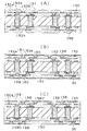
- a mask on which a conductor circuit and a plane conductor pattern are formed is placed on the interlayer resin insulation layer 150 and exposed to light, followed by development to develop a conductor circuit formation recess 153b, a plane conductor formation recess 153a, and a via formation opening. 151 is performed in a lump (FIG. 18B). Since the subsequent steps are the same as those in the first embodiment, description thereof is omitted.
- a method for manufacturing a multilayer printed wiring board according to the third embodiment of the present invention will be described with reference to FIG.
- a conductor circuit forming recess and a plain conductor forming recess were formed in the interlayer insulating layer by laser.
- a conductor circuit forming recess and a plain conductor forming recess are formed by using a molding die (imprint method).
- An interlayer resin insulation layer 150 is formed in the same manner as in the first embodiment described above with reference to FIGS. 1 to 5B.
- the molding die 210 in which a pattern for forming a conductor circuit, a plain conductor, and a via is molded is positioned at a predetermined position (FIG. 19A).
- the mold 210 is pressed against the interlayer resin insulating layer 150 (FIG. 19B).
- the conductor circuit forming recess 153b, the plain conductor forming recess 153a, and the via forming opening 151 are formed in the interlayer resin insulating layer 150 (FIG. 19C). Since the subsequent steps are the same as those in the first embodiment, description thereof is omitted.
- FIG. 23 shows a cross-sectional view of a multilayer printed wiring board according to the fourth embodiment.
- the multilayer printed wiring board 10 includes a lower interlayer resin insulation layer 50 in which via holes 60 and conductor circuits 58 are formed, and an upper interlayer resin insulation layer 150 in which via holes 160, plane conductors 159, and conductor circuits 158 are formed. Is provided. Similar to the first embodiment, the plane conductor 159 is provided with a convex portion 150 a made of resin constituting the interlayer resin insulating layer 150.
- a solder resist layer 70 is formed on the upper interlayer resin insulation layer 150, and bumps 78 U are formed on the conductor circuit 158 U exposed from the openings 71 of the solder resist layer 70.
- a solder resist layer 70 is formed below the lower interlayer resin insulation layer 50, and bumps 78 ⁇ / b> D are formed on the conductor circuit 34 exposed from the openings 71 of the solder resist layer 70.
- a conductor circuit 34 is formed on the upper surface of a support substrate 30 made of glass epoxy resin or BT (bismaleimide triazine) resin (FIG. 20A).
- the interlayer resin insulating layer 50 is formed on the upper surface of the core substrate 30 in the same manner as the step (9) of the first embodiment (FIG. 20B).
- Conductor circuits 58 and via holes 60 are formed on the interlayer resin insulation layer 50 in the same manner as steps (10) to (16) of the first embodiment (FIG. 20C).
- Via holes 151 are formed in the interlayer resin insulation layer 150 with a CO2 gas laser as in the step (10) of the first embodiment, and an excimer laser is formed in the same manner as in the step (20) of the first embodiment.
- the concave portion 153b for forming the conductor circuit and the pattern for forming the plain conductor are formed on the interlayer resin insulating layer 150 (FIG. 21A).
- the electroless copper plating film 152 is formed in the same manner as in the step (21) of the first embodiment, and further the electrolytic copper plating film 156 is formed in the same manner as in the step of the first embodiment (15). Similarly to the step (22), the electrolytic copper plating film 156 is buffed until the upper surface (first surface) of the interlayer resin insulating layer 150 is exposed (FIG. 21B).
- the support substrate 30 is peeled off from the conductor circuit 34 and the interlayer resin insulation layer 50 (FIG. 21C).
- solder resist layer 70 having openings 71 is formed on both surfaces of the multilayer wiring board (FIG. 22A).
- the substrate on which the solder resist layer 70 is formed is immersed in an electroless nickel plating solution to form a nickel plating layer 72 in the opening 71. Further, the substrate is immersed in an electroless gold plating solution to form a gold plating layer 74 on the nickel plating layer 72 (FIG. 22B).
- solder paste containing tin-lead is printed in the opening 71 of the solder resist layer 70 on the upper surface, and a solder paste containing tin-antimony is printed in the opening of the solder resist layer on the lower surface.
- solder paste containing tin-antimony is printed in the opening of the solder resist layer on the lower surface.
- 24B is a graph of test results.
- FIG. 25 is a photograph when the thickness of the copper plating filled in the second recess is set to 10 ⁇ m
- FIG. 26 is a photograph when the thickness of the same copper plating is set to 15 ⁇ m
- FIG. It is the photograph at the time of setting the thickness of the same copper plating to 20 micrometers.
- FIG. 25 where the thickness of the copper plating filled in the second concave portion is 10 ⁇ m
- FIG. 25 (A) is a photograph when the interval between convex portions is set to 10 ⁇ m and the convex portion diameter f is set to 10 ⁇ m.
- FIG. 25B is a photograph in the case where the distance d between the convex portions is set to 20 ⁇ m and the diameter f of the convex portion is set to 20 ⁇ m
- FIG. 25C is a photograph showing the distance d between the convex portions 30 ⁇ m.
- FIG. 25D is a photograph in the case where the distance d between the convex portions is set to 50 ⁇ m and the diameter f of the convex portion is set to 50 ⁇ m.
- the thickness of the copper plating is set to 10 ⁇ m, as shown in FIG. 25 (A), the distance between the convex portions d is set to 10 ⁇ m, and the diameter f of the convex portions is set to 10 ⁇ m. It is possible to make the surface of the substrate substantially flat.
- FIG. 26A is a photograph when the interval between the convex portions is set to 10 ⁇ m and the convex portion diameter f is set to 10 ⁇ m.
- FIG. 26B is a photograph in the case where the distance d between the convex portions is set to 20 ⁇ m and the diameter f of the convex portion is set to 20 ⁇ m, and
- FIG. 26D is a photograph in the case where the distance d between the convex portions is set to 50 ⁇ m and the diameter f of the convex portion is set to 50 ⁇ m.
- the distance d between the protrusions is 10 ⁇ m
- the diameter f of the protrusion is 10 ⁇ m
- FIG. 27A shows a copper plating with a thickness of 20 ⁇ m filled in the second recess
- FIG. 27A is a photograph in the case where the distance d between the protrusions is set to 10 ⁇ m and the diameter f of the protrusion is set to 10 ⁇ m.
- 27 (B) is a photograph when the interval d between the convex portions is set to 20 ⁇ m and the diameter f of the convex portion is set to 20 ⁇ m
- FIG. 27 (C) is an interval between the convex portions d: 30 ⁇ m
- the diameter f is a photograph when set to 30 ⁇ m
- 27D is a photograph when the distance between the convex portions d is set to 50 ⁇ m and the diameter f of the convex portions is set to 50 ⁇ m.
- the thickness of the copper plating is set to 20 ⁇ m, as shown in FIG. 27A, the distance d between the protrusions is 10 ⁇ m, the diameter f of the protrusion is 10 ⁇ m, and in FIG.
- the distance d between the protrusions is 20 ⁇ m
- the diameter f of the protrusion is 20 ⁇ m
- the distance d between the protrusions is 30 ⁇ m, and the diameter f of the protrusion.
Landscapes
- Engineering & Computer Science (AREA)
- Manufacturing & Machinery (AREA)
- Microelectronics & Electronic Packaging (AREA)
- Production Of Multi-Layered Print Wiring Board (AREA)
- Physics & Mathematics (AREA)
- Geometry (AREA)
- Structure Of Printed Boards (AREA)
Abstract
Description
第1樹脂絶縁材上又は第1樹脂絶縁材内に第1導体回路を形成することと、
前記第1樹脂絶縁材及び前記第1導体回路上に第2樹脂絶縁材を形成することと、
前記第2樹脂絶縁材の第1面側に第2導体回路用の第1凹部を形成することと、
前記第2樹脂絶縁材の第1面側に第2の凹部と凸部とからなるプレーン導体用のパターンを形成することと、
前記第1凹部及び前記第2凹部に導電材料を充填して、第2導体回路及びプレーン導体を形成することとからなることを技術的特徴とする。
先ず、本発明の第1実施例に係る多層プリント配線板10の構成について、図1~図10を参照して説明する。図8は、該多層プリント配線板10の断面図を、図9は、図8に示す多層プリント配線板10にICチップ90を取り付け、ドータボード94へ載置した状態を示している。図10(B)は、図8中のb-b横断面を示している。図8に示すように、多層プリント配線板10では、コア基板30の表面に導体回路34が形成されている。コア基板30の表面と裏面とはスルーホール36を介して接続されている。スルーホール36は、スルーホールランドを構成する蓋めっき層36aと、側壁導体層36bとから成り、側壁導体層36bの内部には樹脂充填材37が充填されている。樹脂充填剤なしで銅だけで充填してもよい。蓋めっき層(スルーホールランド)36aの上にバイアホール60及び導体回路58の形成された上面側及び下面側層間樹脂絶縁層50と、バイアホール160、プレーン導体159、及び、導体回路158U(半田パッド)の形成された上面側層間樹脂絶縁層150と、バイアホール160及び導体回路158D(半田パッド)の形成された下面側層間樹脂絶縁層150とが配設されている。導体回路158U(半田パッド)は、層間樹脂絶縁層150の第1面150Aに開口されている第1凹部153bの内部に設けられている。そして、導体回路158U(半田パッド)の表面と層間樹脂絶縁層150の第1面150Aとは略同一平面上に位置している。この導体回路158U(半田パッド)は、バイアホール160を介して下層の導体回路58に電気的に接続されている。
(1)厚さ0.2~0.8mmのガラスエポキシ樹脂またはBT(ビスマレイミドトリアジン)樹脂からなる絶縁性基板30の両面に5~250μmの銅箔32がラミネートされている銅張積層板30Aを出発材料とする(図1(A))。まず、この銅張積層板をドリル削孔して通孔16を穿設し(図1(B))、無電解めっき処理および電解めっき処理を施し、スルーホール36の側壁導体層36bを形成する(図1(C))。
〔電解めっき水溶液〕
硫酸 180 g/l
硫酸銅 80 g/l
添加剤(アトテックジャパン製、商品名:カパラシドGL)
1 ml/l
〔電解めっき条件〕
電流密度 1A/dm2
時間 70分
温度 室温
さらに、粗面化処理した該基板の表面に、パラジウム触媒を付与することにより、層間樹脂絶縁層の表面およびバイアホール用開口の内壁面に触媒核を付着させた。すなわち、上記基板を塩化パラジウム(PbCl2 )と塩化第一スズ(SnCl2 )とを含む触媒液中に浸漬し、パラジウム金属を析出させることにより触媒を付与する。
〔無電解めっき条件〕
34℃の液温度で45分
〔電解めっき液〕
硫酸 2.24 mol/l
硫酸銅 0.26 mol/l
添加剤 19.5 ml/l
(アトテックジャパン社製、カパラシドGL)
〔電解めっき条件〕
電流密度 1 A/dm2
時間 70 分
温度 22±2 ℃
そして、さらに、80℃で1時間、100℃で1時間、120℃で1時間、150℃で3時間の条件でそれぞれ加熱処理を行ってソルダーレジスト層を硬化させ、開口を有し、その厚さが15~25μmのソルダーレジストパターン層を形成する。
第1実施例の第1改変例に係る多層プリント配線板の製造方法について、図13(B)を参照して説明する。
上述した第1実施例では、凸部150aが千鳥状に配置された。これに対して、第1実施例の第1改変例では、凸部150aがマトリクス状に配置されている。この第1実施例の第1改変例は、凸部150aを形成し易い利点がある。
第1実施例の第2改変例に係る多層プリント配線板の製造方法について、図14及び図15を参照して説明する。
上述した第1実施例では、プレーン導体形成用の凹部153a内に千鳥状の凸部150aが形成された。これに対して、第1実施例の第2改変例では、プレーン導体形成用のパターンとして壁状の凸部150bが形成される。
第1実施例の第3改変例に係る多層プリント配線板の製造方法について、図16(A)を参照して説明する。
第1実施例では、凸部150aの上面がプレーン導体159の表面から露出するように形成された。これに対して、第1実施例の第3改変例では、凸部150aの頂部がプレーン導体159の表面から露出しないように、プレーン導体形成用の第2凹部153aの深さh1よりも凸部150aの高さh2が低く形成されている。第1実施例の第3改変例では、第1実施例と比較して、プレーン導体形成用のパターンにおける凸部150aの体積が低減される。その結果、プレーン導体159の体積を大きくでき、電源強化などの電気特性の観点で好ましい。
第1実施例の第4改変例に係る多層プリント配線板の製造方法について、図16(B)を参照して説明する。
第1実施例の第3改変例では、円柱状の凸部150aが形成された。これに対して、第1実施例の第4改変例では、円錐状の凸部150cが形成されている。
第1実施例の第5改変例に係る多層プリント配線板の製造方法について、図17を参照して説明する。
第1実施例においては、半田バンプ78Dが形成されている導体回路158Dを、レーザで設けられた凹部内に形成した。第5改変例では、この導体回路158Dをセミアディティブ法で形成してもよい。この場合、図17に示すように、導体回路158Dは層間絶縁層150の表面上に形成される。
引き続き、本発明の第2実施例に係る多層プリント配線板の製造方法について図18を参照して説明する。
第1実施例では、レーザにより層間絶縁層に導体回路形成用凹部及びプレーン導体形成用の凹部を形成した。これに対して、第2実施例では、露光・現像により導体回路形成用凹部及びプレーン導体形成用凹部を形成する。
図1~図5(B)を参照して上述した第1実施例と同様に層間樹脂絶縁層150を形成する。この層間樹脂絶縁層150は、感光性樹脂からなる(図18(A))。導体回路及びプレーン導体のパターンが形成されたマスクを層間樹脂絶縁層150上に載置して露光した後に現像を行い、導体回路形成用凹部153b、プレーン導体形成用凹部153a及びビア形成用の開口151を一括で行う(図18(B))。以降の工程は、第1実施例と同様であるため説明を省略する。
引き続き、本発明の第3実施例に係る多層プリント配線板の製造方法について図19を参照して説明する。
第1実施例では、レーザにより層間絶縁層に導体回路形成用凹部及びプレーン導体形成用凹部を形成した。これに対して、第3実施例では、成形型を用いて導体回路形成用凹部及びプレーン導体形成用凹部を形成する(インプリント法)。
図1~図5(B)を参照して上述した第1実施例と同様に層間樹脂絶縁層150を形成する。そして、導体回路及びプレーン導体及びビアを形成するためのパターンが成形された成形型210を所定位置に位置決めする(図19(A))。成形型210を層間樹脂絶縁層150に押し当てる(図19(B))。その後、成形型210を抜くことで、層間樹脂絶縁層150に導体回路形成用凹部153b、プレーン導体形成用凹部153a及びビア形成用の開口151を成形する(図19(C))。以降の工程は、第1実施例と同様であるため説明を省略する。
引き続き、本発明の第4実施例に係る多層プリント配線板及び多層プリント配線板の製造方法について図20~図23を参照して説明する。
第1実施例では、コア基板上に層間樹脂絶縁層をビルドアップ積層した。これに対して、第4実施例では、コア基板の無い、いわゆるコアレスのビルドアップ多層プリント配線板として構成される。
多層プリント配線板10は、バイアホール60及び導体回路58の形成された下層層間樹脂絶縁層50と、バイアホール160、プレーン導体159、及び、導体回路158の形成された上層層間樹脂絶縁層150とを備える。第1実施例と同様にプレーン導体159には、層間樹脂絶縁層150を構成する樹脂からなる凸部150aが配置されている。上層層間樹脂絶縁層150の上層にソルダーレジスト層70が形成され、ソルダーレジスト層70の開口部71から露出している導体回路158U上にバンプ78Uが形成されている。下層層間樹脂絶縁層50の下層にソルダーレジスト層70が形成され、該ソルダーレジスト層70の開口部71から露出している導体回路34上にバンプ78Dが形成されている。
(1)ガラスエポキシ樹脂またはBT(ビスマレイミドトリアジン)樹脂からなる支持基板30の上面に導体回路34を形成する(図20(A))。
図24(A)は、凸部(Post)の径f(10、20、30、50μm)を横軸に、凸部間の間隔(Space)d(10、20、30、50μm)を縦軸に取ったイメージ図である。図24(B)は、試験結果のグラフである。縦軸側に凸部間の間隔(Space)及び凸部の径(Post)を取り、横軸側に、厚みが10μm、15μm、20μmの銅めっきを充填した際の窪みの平均値(Mean)及びバラツキ(Stdev.)の測定値が挙げられている。
36 スルーホール
50 層間樹脂絶縁層
58 導体回路
60 バイアホール
70 ソルダーレジスト層
150 層間樹脂絶縁層
150a 凸部
151 開口
153a プレーン導体形成用の凹部
153b 導体回路形成用の凹部
158U、158D 導体回路
160 バイアホール
Claims (17)
- 第1樹脂絶縁材上又は第1樹脂絶縁材内に第1導体回路を形成することと、
前記第1樹脂絶縁材及び前記第1導体回路上に第2樹脂絶縁材を形成することと、
前記第2樹脂絶縁材の第1面側に第2導体回路用の第1凹部を形成することと、
前記第2樹脂絶縁材の第1面側に第2凹部と凸部とからなるプレーン導体用のパターンを形成することと、
前記第1凹部及び前記第2凹部に導電材料を充填して、第2導体回路及びプレーン導体を形成することとからなる多層プリント配線板の製造方法。 - 前記第2凹部と前記凸部とは同時に形成される請求項1の多層プリント配線板の製造方法。
- 前記凸部は、前記第2樹脂絶縁材の第1面に向かってテーパする側面を有する請求項1の多層プリント配線板の製造方法。
- 前記凸部の上面と前記第2樹脂絶縁材の第1面とは略同一平面上に位置する請求項1の多層プリント配線板の製造方法。
- 前記凸部は千鳥状又は格子状に配置される請求項1の多層プリント配線板の製造方法。
- 前記第1凹部及び前記第2凹部をレーザにより形成する請求項1の多層プリント配線板の製造方法。
- 前記第2凹部の開口面積は前記第1凹部の開口面積よりも大きい請求項1の多層プリント配線板の製造方法。
- 前記導電材料はめっきである請求項1の多層プリント配線板の製造方法。
- 前記第2樹脂絶縁材を貫通する開口部を形成した後、該開口部に前記第1導体回路と前記第2導体回路とを電気的に接続するビア導体を形成する請求項1の多層プリント配線板の製造方法。
- 前記第1凹部及び前記第2凹部に前記導電材料を充填した後に、前記第2樹脂絶縁材の第1面が露出するように導電材料を除去する請求項1の多層プリント配線板の製造方法。
- 前記導電材料の除去をエッチングで行う請求項10の多層プリント配線板の製造方法。
- 前記導電材料の除去を研磨で行う請求項10の多層プリント配線板の製造方法。
- 第1樹脂絶縁材と、該第1樹脂絶縁材上又は第1樹脂絶縁材内に形成された第1導体回路と、前記第1樹脂絶縁材及び前記第1導体回路上に形成され、第2導体回路用の第1凹部及びプレーン導体用のパターンを第1面側に有する第2樹脂絶縁材と、前記第1凹部内に形成されている第2導体回路と、前記パターン内に形成されているプレーン導体と、を備え、
前記パターンは第2凹部と凸部とから形成されており、
前記プレーン導体の表面と前記第2樹脂絶縁材の第1面とは略同一平面上に位置する多層プリント配線板。 - 前記凸部は、前記第2樹脂絶縁材の第1面に向かってテーパする側面を有することを特徴とする請求項13の多層プリント配線板。
- 前記凸部は、前記第2樹脂絶縁材と一体で形成されていることを特徴とする請求項13の多層プリント配線板。
- 前記凸部は千鳥状又は格子状に配置されていることを特徴とする請求項13の多層プリント配線板。
- 第2樹脂絶縁材上、前記第2導体回路上及び前記プレーン導体上にはソルダーレジスト層が形成されており、前記ソルダーレジスト層の内部には前記第2導体回路の一部を露出する開口が形成されていて、前記開口から露出される前記第2導体回路上には半田バンプが形成されていることを特徴とする請求項13の多層プリント配線板。
Priority Applications (2)
| Application Number | Priority Date | Filing Date | Title |
|---|---|---|---|
| JP2010541255A JPWO2010064467A1 (ja) | 2008-12-05 | 2009-07-13 | 多層プリント配線板、及び、多層プリント配線板の製造方法 |
| CN2009801487445A CN102239753B (zh) | 2008-12-05 | 2009-07-13 | 多层印刷线路板和多层印刷线路板的制造方法 |
Applications Claiming Priority (2)
| Application Number | Priority Date | Filing Date | Title |
|---|---|---|---|
| US19355608P | 2008-12-05 | 2008-12-05 | |
| US61/193,556 | 2008-12-05 |
Publications (1)
| Publication Number | Publication Date |
|---|---|
| WO2010064467A1 true WO2010064467A1 (ja) | 2010-06-10 |
Family
ID=42229815
Family Applications (1)
| Application Number | Title | Priority Date | Filing Date |
|---|---|---|---|
| PCT/JP2009/062683 Ceased WO2010064467A1 (ja) | 2008-12-05 | 2009-07-13 | 多層プリント配線板、及び、多層プリント配線板の製造方法 |
Country Status (4)
| Country | Link |
|---|---|
| US (2) | US8156647B2 (ja) |
| JP (1) | JPWO2010064467A1 (ja) |
| CN (1) | CN102239753B (ja) |
| WO (1) | WO2010064467A1 (ja) |
Cited By (2)
| Publication number | Priority date | Publication date | Assignee | Title |
|---|---|---|---|---|
| JP2016100600A (ja) * | 2014-11-26 | 2016-05-30 | インテル コーポレイション | 電子パッケージ用の電気インターコネクト |
| JPWO2022265047A1 (ja) * | 2021-06-17 | 2022-12-22 |
Families Citing this family (15)
| Publication number | Priority date | Publication date | Assignee | Title |
|---|---|---|---|---|
| JP5891585B2 (ja) * | 2011-01-24 | 2016-03-23 | 株式会社ソシオネクスト | 半導体装置及び配線基板 |
| US20130168132A1 (en) * | 2011-12-29 | 2013-07-04 | Sumsung Electro-Mechanics Co., Ltd. | Printed circuit board and method of manufacturing the same |
| US9686854B2 (en) * | 2012-09-25 | 2017-06-20 | Denso Corporation | Electronic device |
| US9368439B2 (en) * | 2012-11-05 | 2016-06-14 | Nvidia Corporation | Substrate build up layer to achieve both finer design rule and better package coplanarity |
| KR102059402B1 (ko) * | 2013-04-15 | 2019-12-26 | 삼성전자주식회사 | 전자소자 패키지 및 이에 사용되는 패키지 기판 |
| JP6385075B2 (ja) * | 2013-04-15 | 2018-09-05 | キヤノン株式会社 | プリント配線板、プリント回路板及び電子機器 |
| KR20150064445A (ko) * | 2013-12-03 | 2015-06-11 | 삼성전기주식회사 | 반도체 패키지용 코어리스 기판 및 그 제조 방법, 이를 이용한 반도체 패키지 제조 방법 |
| KR102107037B1 (ko) * | 2014-02-21 | 2020-05-07 | 삼성전기주식회사 | 인쇄회로기판 및 그 제조방법 |
| JP2016115823A (ja) * | 2014-12-16 | 2016-06-23 | イビデン株式会社 | プリント配線板 |
| US9832866B2 (en) * | 2015-06-29 | 2017-11-28 | Samsung Electro-Mechanics Co., Ltd. | Multilayered substrate and method of manufacturing the same |
| US10455708B2 (en) | 2015-06-29 | 2019-10-22 | Samsung Electro-Mechanics Co., Ltd. | Multilayered substrate and method for manufacturing the same |
| JP6779087B2 (ja) * | 2016-10-05 | 2020-11-04 | 株式会社ディスコ | 配線基板の製造方法 |
| CN108135090A (zh) * | 2016-12-01 | 2018-06-08 | 无锡深南电路有限公司 | 一种嵌入铜线的线路板产品制作工艺 |
| CN107318228B (zh) * | 2017-08-29 | 2019-09-06 | 郑州云海信息技术有限公司 | 一种印制电路板的制造方法及其制造装置 |
| CN113709994B (zh) * | 2021-11-01 | 2022-01-25 | 四川英创力电子科技股份有限公司 | 一种在电路板阻焊表面上成型导电层的生产设备及方法 |
Citations (6)
| Publication number | Priority date | Publication date | Assignee | Title |
|---|---|---|---|---|
| JPH08288603A (ja) * | 1995-04-11 | 1996-11-01 | Dainippon Printing Co Ltd | プリント配線板とその製造方法および転写用原版 |
| JPH098465A (ja) * | 1995-06-16 | 1997-01-10 | Ibiden Co Ltd | 多層プリント配線板 |
| JP2000165049A (ja) * | 1998-11-27 | 2000-06-16 | Shinko Electric Ind Co Ltd | 多層回路基板の製造方法 |
| JP2000261141A (ja) * | 1999-03-08 | 2000-09-22 | Shinko Electric Ind Co Ltd | 多層配線基板及びその製造方法並びに半導体装置 |
| JP2003051650A (ja) * | 2001-08-06 | 2003-02-21 | Ibiden Co Ltd | プリント配線板、多層プリント配線板およびその製造方法 |
| JP2005340432A (ja) * | 2004-05-26 | 2005-12-08 | Shinko Electric Ind Co Ltd | 配線基板の製造方法 |
Family Cites Families (9)
| Publication number | Priority date | Publication date | Assignee | Title |
|---|---|---|---|---|
| TW256013B (en) * | 1994-03-18 | 1995-09-01 | Hitachi Seisakusyo Kk | Installation board |
| KR100194130B1 (ko) * | 1994-03-30 | 1999-06-15 | 니시무로 타이죠 | 반도체 패키지 |
| EP1701601B1 (en) * | 1996-12-13 | 2008-06-04 | Ibiden Co., Ltd. | Multilayer printed wiring board |
| JP3889856B2 (ja) * | 1997-06-30 | 2007-03-07 | 松下電器産業株式会社 | 突起電極付きプリント配線基板の製造方法 |
| EP1139705B1 (en) * | 1999-09-02 | 2006-11-22 | Ibiden Co., Ltd. | Printed wiring board and method of producing the same |
| US6343819B1 (en) * | 2000-02-24 | 2002-02-05 | Steven Shiozaki | Security tag |
| JP5021473B2 (ja) * | 2005-06-30 | 2012-09-05 | イビデン株式会社 | プリント配線板の製造方法 |
| US7823762B2 (en) * | 2006-09-28 | 2010-11-02 | Ibiden Co., Ltd. | Manufacturing method and manufacturing apparatus of printed wiring board |
| JP5144222B2 (ja) * | 2007-11-14 | 2013-02-13 | 新光電気工業株式会社 | 配線基板及びその製造方法 |
-
2009
- 2009-07-13 WO PCT/JP2009/062683 patent/WO2010064467A1/ja not_active Ceased
- 2009-07-13 CN CN2009801487445A patent/CN102239753B/zh active Active
- 2009-07-13 JP JP2010541255A patent/JPWO2010064467A1/ja active Pending
- 2009-11-16 US US12/619,129 patent/US8156647B2/en active Active
-
2011
- 2011-12-08 US US13/314,641 patent/US8853552B2/en active Active
Patent Citations (6)
| Publication number | Priority date | Publication date | Assignee | Title |
|---|---|---|---|---|
| JPH08288603A (ja) * | 1995-04-11 | 1996-11-01 | Dainippon Printing Co Ltd | プリント配線板とその製造方法および転写用原版 |
| JPH098465A (ja) * | 1995-06-16 | 1997-01-10 | Ibiden Co Ltd | 多層プリント配線板 |
| JP2000165049A (ja) * | 1998-11-27 | 2000-06-16 | Shinko Electric Ind Co Ltd | 多層回路基板の製造方法 |
| JP2000261141A (ja) * | 1999-03-08 | 2000-09-22 | Shinko Electric Ind Co Ltd | 多層配線基板及びその製造方法並びに半導体装置 |
| JP2003051650A (ja) * | 2001-08-06 | 2003-02-21 | Ibiden Co Ltd | プリント配線板、多層プリント配線板およびその製造方法 |
| JP2005340432A (ja) * | 2004-05-26 | 2005-12-08 | Shinko Electric Ind Co Ltd | 配線基板の製造方法 |
Cited By (2)
| Publication number | Priority date | Publication date | Assignee | Title |
|---|---|---|---|---|
| JP2016100600A (ja) * | 2014-11-26 | 2016-05-30 | インテル コーポレイション | 電子パッケージ用の電気インターコネクト |
| JPWO2022265047A1 (ja) * | 2021-06-17 | 2022-12-22 |
Also Published As
| Publication number | Publication date |
|---|---|
| CN102239753B (zh) | 2013-11-06 |
| US20100139968A1 (en) | 2010-06-10 |
| CN102239753A (zh) | 2011-11-09 |
| JPWO2010064467A1 (ja) | 2012-05-10 |
| US8156647B2 (en) | 2012-04-17 |
| US8853552B2 (en) | 2014-10-07 |
| US20120073868A1 (en) | 2012-03-29 |
Similar Documents
| Publication | Publication Date | Title |
|---|---|---|
| JPWO2010064467A1 (ja) | 多層プリント配線板、及び、多層プリント配線板の製造方法 | |
| US8003896B2 (en) | Multi-layer printed wiring board and manufacturing method thereof | |
| US8779602B2 (en) | Wiring board, semiconductor apparatus and method of manufacturing them | |
| US8367943B2 (en) | Multilayered printed wiring board | |
| US8153905B2 (en) | Method for manufacturing printed wiring board and printed wiring board | |
| US8592691B2 (en) | Printed wiring board | |
| JP2010206169A (ja) | プリント配線板の製造方法 | |
| JP2012069926A (ja) | プリント配線板及びプリント配線板の製造方法 | |
| US7462784B2 (en) | Heat resistant substrate incorporated circuit wiring board | |
| US7402760B2 (en) | Multi-layer printed wiring board and manufacturing method thereof | |
| WO2007086509A1 (ja) | プリント配線板の製造方法 | |
| US8410374B2 (en) | Printed wiring board | |
| JP5432800B2 (ja) | 配線基板の製造方法 | |
| JP2013122962A (ja) | 配線基板 | |
| JP2003209359A (ja) | コア基板およびその製造方法 | |
| JP2013122963A (ja) | 配線基板 | |
| JP2004095582A (ja) | コア基板およびその製造方法 | |
| US12543582B2 (en) | Wiring board | |
| JP2013122961A (ja) | 配線基板、配線基板の製造方法 | |
| JP2010166099A (ja) | プリント配線板及びプリント配線板の製造方法 |
Legal Events
| Date | Code | Title | Description |
|---|---|---|---|
| WWE | Wipo information: entry into national phase |
Ref document number: 200980148744.5 Country of ref document: CN |
|
| 121 | Ep: the epo has been informed by wipo that ep was designated in this application |
Ref document number: 09830236 Country of ref document: EP Kind code of ref document: A1 |
|
| ENP | Entry into the national phase |
Ref document number: 2010541255 Country of ref document: JP Kind code of ref document: A |
|
| NENP | Non-entry into the national phase |
Ref country code: DE |
|
| 122 | Ep: pct application non-entry in european phase |
Ref document number: 09830236 Country of ref document: EP Kind code of ref document: A1 |