WO2010062073A2 - 자기 정보 처리 장치 및 그 제조 방법 - Google Patents
자기 정보 처리 장치 및 그 제조 방법 Download PDFInfo
- Publication number
- WO2010062073A2 WO2010062073A2 PCT/KR2009/006715 KR2009006715W WO2010062073A2 WO 2010062073 A2 WO2010062073 A2 WO 2010062073A2 KR 2009006715 W KR2009006715 W KR 2009006715W WO 2010062073 A2 WO2010062073 A2 WO 2010062073A2
- Authority
- WO
- WIPO (PCT)
- Prior art keywords
- magnetic
- substrate
- layer
- information processing
- crystal
- Prior art date
- Legal status (The legal status is an assumption and is not a legal conclusion. Google has not performed a legal analysis and makes no representation as to the accuracy of the status listed.)
- Ceased
Links
Images


Classifications
-
- G—PHYSICS
- G11—INFORMATION STORAGE
- G11C—STATIC STORES
- G11C11/00—Digital stores characterised by the use of particular electric or magnetic storage elements; Storage elements therefor
- G11C11/18—Digital stores characterised by the use of particular electric or magnetic storage elements; Storage elements therefor using Hall-effect devices
-
- H—ELECTRICITY
- H10—SEMICONDUCTOR DEVICES; ELECTRIC SOLID-STATE DEVICES NOT OTHERWISE PROVIDED FOR
- H10N—ELECTRIC SOLID-STATE DEVICES NOT OTHERWISE PROVIDED FOR
- H10N52/00—Hall-effect devices
-
- G—PHYSICS
- G11—INFORMATION STORAGE
- G11C—STATIC STORES
- G11C11/00—Digital stores characterised by the use of particular electric or magnetic storage elements; Storage elements therefor
- G11C11/02—Digital stores characterised by the use of particular electric or magnetic storage elements; Storage elements therefor using magnetic elements
- G11C11/16—Digital stores characterised by the use of particular electric or magnetic storage elements; Storage elements therefor using magnetic elements using elements in which the storage effect is based on magnetic spin effect
- G11C11/161—Digital stores characterised by the use of particular electric or magnetic storage elements; Storage elements therefor using magnetic elements using elements in which the storage effect is based on magnetic spin effect details concerning the memory cell structure, e.g. the layers of the ferromagnetic memory cell
-
- G—PHYSICS
- G11—INFORMATION STORAGE
- G11C—STATIC STORES
- G11C11/00—Digital stores characterised by the use of particular electric or magnetic storage elements; Storage elements therefor
- G11C11/02—Digital stores characterised by the use of particular electric or magnetic storage elements; Storage elements therefor using magnetic elements
- G11C11/16—Digital stores characterised by the use of particular electric or magnetic storage elements; Storage elements therefor using magnetic elements using elements in which the storage effect is based on magnetic spin effect
- G11C11/165—Auxiliary circuits
- G11C11/1675—Writing or programming circuits or methods
-
- G—PHYSICS
- G11—INFORMATION STORAGE
- G11C—STATIC STORES
- G11C11/00—Digital stores characterised by the use of particular electric or magnetic storage elements; Storage elements therefor
- G11C11/56—Digital stores characterised by the use of particular electric or magnetic storage elements; Storage elements therefor using storage elements with more than two stable states represented by steps, e.g. of voltage, current, phase, frequency
- G11C11/5607—Digital stores characterised by the use of particular electric or magnetic storage elements; Storage elements therefor using storage elements with more than two stable states represented by steps, e.g. of voltage, current, phase, frequency using magnetic storage elements
-
- H—ELECTRICITY
- H10—SEMICONDUCTOR DEVICES; ELECTRIC SOLID-STATE DEVICES NOT OTHERWISE PROVIDED FOR
- H10N—ELECTRIC SOLID-STATE DEVICES NOT OTHERWISE PROVIDED FOR
- H10N50/00—Galvanomagnetic devices
- H10N50/10—Magnetoresistive devices
Definitions
- the present invention relates to an information processing apparatus and a manufacturing method thereof, and more particularly, to a magnetic information processing apparatus and a manufacturing method thereof.
- the conventional electronic memory device is a binary system method that stores two logic states "0" and "1" in the basic "bit" of information storage.
- the method of storing two different charge states is used as the information storage principle of a binary system.
- the method of storing magnetic states along two magnetization directions is binary. (binary) It is used as information storage principle of system.
- the density of information storage is determined by the density of "bits" storing one piece of information, so the size of each "bit” device determines the overall capacity of information storage.
- a way to increase the capacity of information storage in binary systems is to reduce the size of the elements that make up one bit ".
- MRAM Magnetic Random Access Memory
- MRAM Magnetic Random Access Memory
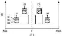
- FIG. 1 schematically illustrates a spin valve structure, which is an essential part of a conventional MRAM device, using a relationship between a magnetic field and a resistance.
- a conventional MRAM device includes a hard magnetic layer 105 formed below the space layer 103 based on the space layer 103 to perform a sensing role, and a soft magnetic layer 101 formed on the rising side to perform a storage role. It is configured by.
- the conventional MRAM device uses a Giant MagnetoResistance (GMR) phenomenon in which the resistance of the two magnetic layers 101 and 105 with the nonmagnetic layer 103 interposed therebetween is different than that of the same case. Based on the structure, it has a structure composed of multiple magnetic layers.
- GMR Giant MagnetoResistance
- the magnetization direction of the soft magnetic layer 101 is recorded by flowing a current through a word line, and the recorded magnetization direction is read by sensing a change in resistance according to the magnetization directions of the two magnetic layers 101 and 105.
- the conventional MRAM device has a complicated structure of multiple layers by adding a plurality of magnetic layers constituting the spin valve and a layer that performs a word line and a read line, thereby lowering process difficulty and productivity. There is.
- the magnetic multilayer structure has a complicated structure, and the first magnetization direction 110 and the fourth magnetization direction 140 are in a degenerate state having the same resistance value, and the second magnetization direction 120 In the degenerate state in which the states of the third magnetization direction 130 and the third magnetization direction 130 have the same resistance value, there is a complicated problem of writing and reading information.
- the information that can be stored in one cell is 1-bit data representing "0" and "1", and there is a problem in that the amount of stored information is smaller than that of a complicated structure.
- an object of the present invention is to increase the information processing capacity and the processing speed by allowing a magnetic body to have multiple Hall resistance states.
- an object of the present invention is to reduce the thickness of the magnetic information processing apparatus and to improve the efficiency of the process.
- Magnetic information processing apparatus for solving the above problems includes a magnetic body layer formed on a substrate and a substrate, including a magnetic material having a multi-axis magnetic anisotropy, the magnetic material includes a crystal structure Therefore, the crystal plane of the magnetic body and the plane of the magnetic layer do not coincide.
- the magnetic body may be a ferromagnetic body.
- the substrate may include a crystal structure, and the crystal surface of the substrate may not coincide with the surface of the substrate.
- the magnetic information processing apparatus may further include magnetic field applying means for applying a magnetic field to the magnetic body.
- the magnetic information processing apparatus may further include a resistance measuring means for measuring the resistance value of the magnetic body.
- a method of manufacturing a magnetic information processing apparatus including forming a substrate including a crystal structure and forming a magnetic layer including a magnetic material including a crystal structure on the substrate and having a multilayer magnetic anisotropy characteristic. And the substrate is formed such that the crystal surface of the substrate does not coincide with the surface of the substrate.
- the magnetic body may be a ferromagnetic body.
- a method of manufacturing a magnetic information processing apparatus includes forming a substrate and forming a magnetic layer including a magnetic material having multilayer magnetic anisotropy on the substrate, wherein the magnetic material has a crystal structure. It is formed so that the crystal surface of the magnetic body and the surface of the magnetic layer do not coincide.
- the magnetic body may be a ferromagnetic body.
- the present invention it is possible to provide a magnetic information processing apparatus having improved information processing capacity and processing speed, and to reduce the thickness of the magnetic information processing apparatus and to improve the efficiency of the process.
- FIG. 1 schematically illustrates a spin valve structure, which is an essential part of a conventional MRAM device, using a relationship between a magnetic field and a resistance.
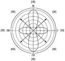
- FIG. 2 is a diagram illustrating four magnetization directions at an angle at which magnetic energy is minimum in a biaxial magnetic anisotropic magnetic body.
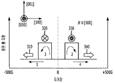
- FIG. 3 is a history of changing the value of Planar Hall Resistance (PHR) according to the magnetization direction when scanning an external magnetic field in a magnetic single domain state when the crystal plane of the biaxial magnetic anisotropic magnetic material coincides with the plane of the biaxial magnetic anisotropic magnetic layer.
- PHR Planar Hall Resistance
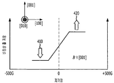
- FIG. 4 is a view for explaining an anomalous hall effect (AHE) when the crystal plane of the magnetic body does not coincide with the plane of the magnetic layer.
- AHE anomalous hall effect
- FIG. 5 shows four magnetization states when the crystal plane of the biaxial magnetic anisotropic magnetic body and the plane of the biaxial magnetic anisotropic magnetic layer do not coincide with each other (when the plane hole effect of FIG. 3 and the abnormal hole effect of FIG. 4 are combined). Hall effect history curve for.
- Fig. 6 is a view for explaining the hole resistance (a) and the hole effect (b) when the crystal plane of the biaxial magnetic anisotropic magnetic body and the plane of the biaxial magnetic anisotropic magnetic layer do not coincide with each other according to the present invention.
- FIG. 7 is a view for explaining an experimental value for the Hall resistance value according to the inclination angle formed between the crystal plane of the biaxial magnetic anisotropic magnetic body and the plane of the biaxial magnetic anisotropic magnetic layer according to the present invention.
- FIG. 8 is a view showing an example of a magnetic field applying method for having four different hole resistance values when the crystal plane of the biaxial magnetic anisotropic magnetic body and the plane of the biaxial magnetic anisotropic magnetic layer do not coincide with each other according to the present invention.
- FIG. 9 is a diagram for explaining a magnetic information processing device according to the present invention.
- FIG. 10 is a view for explaining an embodiment of a method of manufacturing a magnetic information processing device according to the present invention.
- FIG. 11 is a view for explaining another embodiment of the manufacturing method of the magnetic information processing device according to the present invention.
- components expressed as means for performing the functions described in the detailed description include all types of software including, for example, a combination of circuit elements or firmware / microcode, etc. that perform the functions. It is intended to include all methods of performing a function which are combined with appropriate circuitry for executing the software to perform the function.
- the invention, as defined by these claims, is equivalent to what is understood from this specification, as any means capable of providing such functionality, as the functionality provided by the various enumerated means are combined, and in any manner required by the claims. It should be understood that.
- the present invention relates to a magnetic information processing apparatus and a manufacturing method thereof, wherein the magnetic information processing apparatus includes an information storage device or a logic processing device including a random access memory (RAM) or the like.
- the magnetic information processing apparatus includes an information storage device or a logic processing device including a random access memory (RAM) or the like.
- the magnetic body in the present invention includes a crystal structure, and means a magnetic body having multiaxial (biaxial, triaxial, etc.) magnetic anisotropy.
- Magnetic material includes ferromagnetic material, and may include Fe, Co, Ni, Cr, permalloy, heusler alloy, gallium manganese arsenide (GaMnAs), germanium manganese (GeMn), and the magnetic material may be a single magnetic domain. Or a plurality of magnetic domains.
- the biaxial magnetic anisotropy magnetic body may have a magnetization direction in four directions in a plane, and when the biaxial magnetic anisotropy has three or more axes, it may have a multiple magnetization direction.
- FIG. 2 is a diagram illustrating four magnetization directions at an angle at which magnetic energy is minimum in a biaxial magnetic anisotropic magnetic body.
- four arrow directions indicate four magnetization directions.
- FIG. 3 is a history of changing the value of Planar Hall Resistance (PHR) according to the magnetization direction when scanning an external magnetic field in a magnetic single domain state when the crystal plane of the biaxial magnetic anisotropic magnetic material coincides with the plane of the biaxial magnetic anisotropic magnetic layer.
- PHR Planar Hall Resistance
- information can be stored in two magnetization states 320 and 330 having high resistance values and two magnetization states 310 and 340 having low resistance values, thereby storing four types of information. Can be.
- the effect corresponding to four combinations obtained in the spin valve structure of the conventional magnetic triple layer structure shown in FIG. 1 can be realized as a single magnetic layer. .
- the resistance values of the first magnetization state 310 and the fourth magnetization state 340 are the same.
- the resistance values of the second magnetization state 320 and the third magnetization state 330 are the same, in order to read the information stored in the four states, it is necessary to undergo a complicated process as in the conventional spin valve structure. have.
- the crystal plane of the biaxial magnetic anisotropic magnetic body and the film plane of the biaxial magnetic anisotropic magnetic layer are inclined to form the magnetic body so that both surfaces thereof do not coincide.
- This combines the Planer Hall Effect (PHE) and the Anomalous Hall Effect (AHE), resulting in separate Hall resistance values for each of the four magnetization states. And writing is effective.
- PHE Planer Hall Effect
- AHE Anomalous Hall Effect
- FIG. 4 is a view for explaining an anomalous hall effect (AHE) when the crystal plane of the magnetic body does not coincide with the plane of the magnetic layer.
- AHE anomalous hall effect
- the magnetization states exist in the crystal plane in a single domain state, and because the crystal planes of the magnetic bodies and the planes of the magnetic layers do not coincide, different abnormal holes are caused by the inclined crystal planes when switching to another magnetization state.
- the states 410 and 420 having effect values are obtained.
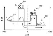
- FIG. 5 shows four magnetization states when the crystal plane of the biaxial magnetic anisotropic magnetic body and the plane of the biaxial magnetic anisotropic magnetic layer do not coincide with each other (when the plane hole effect of FIG. 3 and the abnormal hole effect of FIG. 4 are combined). Hall effect history curve for.
- the magnetization states 510, 520, 530, and 540 of the four resistance values R1, R2, R3, and R4 are different from each other through the hysteresis curve of the Hall effect when the magnetization transition occurs in the crystal plane of the magnetic body. It can be seen that the state.
- the Hall resistance value according to the transition between the four magnetization states of the magnetic material in which the crystal plane of the biaxial magnetic anisotropic magnetic layer and the plane of the biaxial magnetic anisotropic magnetic layer do not coincide with each other are different. Can be stored. Due to the Hall resistance values according to the four different magnetization states, compared to the magnetic spin valve structure, the stored information can be read accurately and quickly.
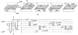
- FIG. 6 illustrates the planar hole effect and abnormal hole effect caused by the horizontal and vertical components of the magnetic body surface of magnetization when the crystal plane of the biaxial magnetic anisotropic magnetic body and the plane of the biaxial magnetic anisotropic magnetic layer do not coincide with each other according to the present invention. It is for the drawing.
- the crystal plane of the biaxial magnetic anisotropic magnetic body and the plane of the biaxial magnetic anisotropic magnetic layer do not coincide with each other, and both surfaces are inclined at an angle ⁇ , and magnetization is performed on the crystal plane.
- the magnetization consists of the horizontal and vertical components of the magnetic surface and shows four magnetization states (I, II, III, IV).
- a planar hall resistance (PHR) and anomalous hall resistance (AHR) are combined according to a combination of horizontal and vertical components of magnetization shown in FIG.
- Four Hall resistance states (I, II, III, IV) are shown for the total Hall resistance.
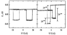
- FIG. 7 is a view for explaining an experimental value for the Hall resistance value according to the inclination angle formed between the crystal plane of the biaxial magnetic anisotropic magnetic body and the plane of the biaxial magnetic anisotropic magnetic layer according to the present invention.
- the left view shows a case where the inclination angle ⁇ formed between the crystal plane of the biaxial magnetic anisotropic magnetic layer and the plane of the biaxial magnetic anisotropic magnetic layer is 0 degrees
- the right view shows the crystal plane of the biaxial magnetic anisotropic magnetic material and the biaxial magnetic anisotropy.
- 5 is a view illustrating a case where the inclination angle ⁇ formed by the surface of the magnetic layer is 5 degrees.
- the angle ⁇ When the angle ⁇ is 0 degrees, it has only two Hall resistance values, whereas when the angle ⁇ is 5 degrees, that is, when the crystal plane of the biaxial magnetic anisotropic magnetic material does not coincide with the plane of the biaxial magnetic anisotropic magnetic layer, 4 It can be seen that two different Hall resistance values are measured.
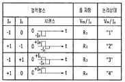
- FIG. 8 is a view showing an example of a magnetic field applying method for having four different hole resistance values when the crystal plane of the biaxial magnetic anisotropic magnetic body and the plane of the biaxial magnetic anisotropic magnetic layer do not coincide with each other according to the present invention.
- four different Hall resistance values R1, R2, R3, and R4 may be stored by using a pulse sequence using the current I.
- the current may be divided into a high current and a low current, and in addition to this, a middle current may be added according to an embodiment.
- each domain is magnetized in the direction of the crystal plane of magnetic easy axes among the four magnetization directions, and the total Hall resistance value of the magnetic state is as shown in [Equation 1] below. It can be expressed as the sum of and an abnormal hall resistance value.
- Equation 1 the first term represents the resistance due to the abnormal Hall effect, and the second term represents the resistance due to the planar Hall effect.
- k represents the difference in the specific resistance value when the direction of the current is perpendicular to the direction perpendicular to the magnetization direction
- t represents the thickness of the sample
- Rs represents an abnormal Hall constant
- ⁇ is the magnetization is on the film plane It represents an angle formed with the vertical direction
- ⁇ represents an angle formed by the magnetization with the current direction in the thin film sample plane.
- the resistance values of the first magnetization state 310 and the fourth magnetization state 340 of the four states are the same, and the resistance values of the second magnetization state 320 and the third magnetization state 330 are the same.
- the resistance value is the same.
- the biaxial magnetic anisotropic magnetic body has four resistance states respectively separated in four magnetization directions.
- the resistance R in the first term and the second term of [Equation 2] represents the measurement of the resistance value of the magnetic body when it is perpendicular or horizontal to the current direction.
- the magnetic body having a multi-axis magnetic anisotropy of three or more axes is more apparent to those skilled in the art than the magnetic material having a biaxial magnetic anisotropy, it is apparent to those skilled in the art It is included in the disclosure of the present invention.
- a magnetic body including a plurality of magnetic domains may be combined with more resistance states than a magnetic body including a single magnetic domain, and thus, the above-described present invention may include a magnetic body including a plurality of magnetic domains.
- Application to is included in the disclosure of the present invention.
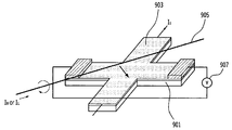
- FIG. 9 is a diagram for explaining a magnetic information processing device according to the present invention.
- the magnetic information processing apparatus includes a magnetic body layer 903 formed on a substrate 901 and a substrate 901 and including a magnetic material having a multiaxial magnetic anisotropy property.
- the magnetic material includes a crystal structure, The crystal surface of the magnetic body and the surface of the magnetic layer 903 do not coincide with each other.
- the non-conformity here includes a case where the crystal surface of the magnetic body and the surface of the magnetic layer 903 do not coincide with each other and are inclined.
- the magnetic body may be ferromagnetic.
- the substrate 901 may be a substrate 901 including a crystal structure and in which the crystal surface of the substrate 901 and the surface of the substrate 901 do not coincide with each other. In such a configuration, in manufacturing the magnetic information processing apparatus according to the present invention, it is possible to more easily form the crystal surface of the magnetic body and the surface of the magnetic layer 903 when the magnetic body is grown, thereby providing a process advantage.
- GaAs or Si may be used as the substrate 901. Meanwhile, the crystal structure included in the substrate 901 may include a poly crystal structure.
- the magnetic information processing apparatus may further include magnetic field applying means 905 for applying a magnetic field to the magnetic material.
- the magnetic field applying means 905 is a means for changing the value of the Hall resistance in the magnetic body by applying a magnetic field to the magnetic body.
- the magnetic field applying means 905 may be implemented by a method of supplying a current pulse, and a current line 905 may be provided for this purpose.
- the sequence for the current pulse can be implemented in the embodiment as described in FIG.
- the magnetic field applying means 905 may be composed of a plurality of current lines, and is composed of an insulating layer (not shown) between the substrate 901 and the magnetic layer 903, or between the magnetic layer 903 A plurality of current lines can be provided up and down. In addition, it may further include an insulating layer (not shown) along the current line.
- the magnetic information processing apparatus may further include a resistance measuring means 907 for measuring the resistance value of the magnetic body.
- the resistance measuring unit 907 may measure the value of the hall resistance.
- the resistance measuring means 907 may include a voltage applying means for applying a voltage to the magnetic material and a sensing current applying means for applying the sensing current Is.
- FIG. 10 is a view for explaining an embodiment of a method of manufacturing a magnetic information processing device according to the present invention.
- a method of manufacturing a magnetic information processing apparatus may include forming a substrate including a crystal structure, and forming a magnetic material including a crystal structure on the substrate and having multilayer magnetic anisotropy. Forming a magnetic layer comprising a.
- the substrate is formed so that the crystal surface of the substrate does not coincide with the surface of the substrate.
- the magnetic body may be a ferromagnetic body.
- a predetermined substrate includes a crystal structure, and the crystal surface of the substrate and the surface of the substrate do not coincide, when the magnetic material is grown on the substrate, the magnetic body also coincides with the crystal surface of the magnetic body according to the crystal surface of the predetermined substrate. It is formed so as not to. As a result, in this embodiment, the magnetic material is grown on the substrate where the crystal surface of the substrate and the surface of the substrate do not coincide, whereby the process advantage is obtained.
- the insulating film, the first and second current lines may be sequentially formed as shown in FIG. 10, and an additional protective film may be formed.
- the substrate in FIG. 10 is located on the lower surface of the magnetic material, and additional layers such as an insulating film, first and second current lines, and the like may be formed between the substrate and the magnetic layer.
- additional layers such as an insulating film, first and second current lines, and the like may be formed between the substrate and the magnetic layer.
- the crystal plane of the additional layer facing the magnetic material of the additional layers should not coincide with the plane of the additional layer, and this additional layer may be interpreted to be included in the substrate.
- FIG. 11 is a view for explaining another embodiment of the manufacturing method of the magnetic information processing device according to the present invention.
- a method of manufacturing a magnetic information processing apparatus includes forming a substrate and forming a magnetic layer including a magnetic material having multilayer magnetic anisotropy on the substrate.
- the magnetic body includes a crystal structure and is formed such that the crystal surface of the magnetic body does not coincide with the surface of the magnetic layer.
- the magnetic body may be a ferromagnetic body.
- FIG. 11 illustrates a case in which a first current line, an insulating film, and the like are additionally formed between the substrate and the magnetic layer described with reference to FIG. 10.
- the substrate includes a general substrate and may also include an amorphous substrate.
- the magnetic layer is formed so that the crystal surface of the magnetic body and the surface of the magnetic layer do not coincide without using the crystal surface or the like of the lower layer of the magnetic layer.
- the substrate and the magnetic layer may be sequentially formed, and the formed magnetic layer may be cut at an angle so that the crystal surface of the magnetic body and the surface of the magnetic layer do not coincide.
- the insulating film faces the lower portion of the magnetic layer as shown in FIG. 11, the insulating film and the magnetic layer are sequentially formed, and the formed magnetic layer is cut at an angle so that the crystal surface of the magnetic body and the surface of the magnetic layer do not coincide.
- the crystal surface of the magnetic body and the surface of the magnetic layer do not coincide by means of various current semiconductor processes.
- a first current line and an insulating film are sequentially formed on a substrate, a magnetic layer is formed thereon, and an insulating film, a second current line, etc. are sequentially formed on the magnetic layer.
- a protective film can be formed.
- the present invention is used in a magnetic information processing device and a manufacturing method thereof.
Landscapes
- Engineering & Computer Science (AREA)
- Computer Hardware Design (AREA)
- Hall/Mr Elements (AREA)
- Thin Magnetic Films (AREA)
- Manufacturing Of Magnetic Record Carriers (AREA)
Abstract
본 발명은 정보 처리 장치 및 그 제조 방법에 관한 것으로서, 더욱 상세하게는 자기 정보 처리 장치 및 그 제조 방법에 관한 것이다. 본 발명에 따른 자기 정보 처리 장치는 기판 및 기판 위에 형성되고, 다축 자기 이방성 특성을 갖는 자성체를 포함하는 자성체층을 포함하고, 자성체는 결정구조를 포함하고, 자성체의 결정면과 자성체층의 면이 일치하지 않는다.
Description
본 발명은 정보 처리 장치 및 그 제조 방법에 관한 것으로서, 더욱 상세하게는 자기 정보 처리 장치 및 그 제조 방법에 관한 것이다.
종래의 전자 기억 소자는 정보저장의 기본 "bit"에 두 개의 논리상태인 "0"과 "1"을 저장하는 2진(binary) 시스템 방식이다. 예를 들면, 반도체 소자에서는 두 개의 다른 전하상태를 저장하는 방법을 2진(binary) 시스템의 정보저장 원리로 이용하고 있고, 자성체소자에서는 두 개의 자화방향에 따른 자기상태를 저장하는 방법을 2진(binary) 시스템의 정보저장 원리로 이용하고 있다.
이와 같은 2진(binary) 시스템에서 정보저장의 밀도는 하나의 정보를 저장하는 "bit"의 밀도에 의해서 결정되므로 각 "bit"를 이루는 소자의 크기가 전체적인 정보저장의 용량을 결정짓는다.
따라서, 2진(binary) 시스템에서 정보저장의 용량을 증가시키는 방법은 하나의 bit"를 구성하는 소자의 크기를 축소하는 것이다.
최근 연구가 가장 활발히 진행되는 MRAM(Magnetic Random Access Memory) 소자 역시 2진(binary) 시스템을 기본으로 하는 기억 소자로서 자성체 삼중층 스핀밸브 구조에서 터널링 저항의 차이로 발생되는 두 저항 상태를 "0"과 "1"의 논리 상태로 응용하는 것이다. 따라서, 이러한 MRAM 소자 역시 복잡한 구조에 비해 정보저장의 용량은 여전히 2진(binary) 시스템의 한계를 갖는다.
이에 따라, 정보저장 용량의 향상을 단일 "bit"에 여러 상태의 정보를 저장하여 하는 방법으로 스핀밸브와 같은 자성체 삼중 층 구조에서 상대적 자화방향의 조합에 따른 4 개의 상태를 응용하려는 노력이 시도되었다.
도 1은 종래의 MRAM 소자의 핵심 부분인 스핀 밸브 구조를 자기장과 저항의 관계를 이용하여 개략적으로 도시한 도면이다.
도 1을 참조하면, 종래의 MRAM 소자는 스페이스층(103)을 기준으로 하층에 형성되어 센싱 역할을 수행하는 하드 자성층(105)과 상승에 형성되어 저장 역할을 수행하는 소프트 자성층(101)을 포함하여 구성된다.
종래의 MRAM 소자는 비자성층(103)을 사이에 둔 두 자성층(101, 105)의 스핀 방향이 같은 경우보다 다른 경우의 저항이 크게 달라지는 거대 자기저항(GMR: Giant MagnetoResistance) 현상을 이용한 것으로 스핀밸브 구조를 기본으로 함으로써 다중 자성층으로 구성된 구조를 갖는다.
소프트 자성층(101)의 자화방향을 워드라인에 전류를 흘림으로서 기록하고 두 자성층(101, 105)의 자화방향에 따른 저항 변화를 감지함으로써 기록된 자화방향을 읽게 된다.
그러나, 종래의 MRAM 소자는 스핀밸브를 구성하는 여러 자성층과 쓰고(word line), 읽는(read line) 역할을 수행하는 층이 더해져서 다중층의 복잡한 구조를 가짐으로써 공정상의 어려움과 생산성이 떨어지는 문제가 있다.
또한, 이러한 자성체 다층 구조는 구조가 복잡할 뿐만 아니라, 제1 자화방향(110)과 제4 자화방향(140)의 상태가 같은 저항값을 갖는 축퇴된 상태에 있고, 제2 자화방향(120)과 제3 자화방향(130)의 상태가 같은 저항값을 갖는 축퇴된 상태에 있어서, 각각 정보를 쓰고 읽는 절차가 복잡한 문제점이 있다.
또한, 하나의 셀 안에 저장할 수 있는 정보는 "0"과 "1"을 나타내는 1비트 데이터로 복잡한 구조에 비하여 저장된 정보량이 적은 문제점이 있다.
따라서, 본 발명은 자성체가 다중 홀저항 상태를 갖도록 하여 정보 처리 용량과 처리 속도를 증가시키는 것을 목적으로 한다.
또한, 본 발명은 자기 정보 처리 장치의 두께를 감소시키고, 공정의 효율성을 향상시키는 것을 목적으로 한다.
본 발명의 다른 목적 및 장점들은 하기의 설명에 의해서 이해될 수 있으며, 본 발명의 실시예에 의해 보다 분명하게 알게 될 것이다. 또한, 본 발명의 목적 및 장점들은 특허청구범위에 나타낸 수단 및 그 조합에 의해 실현될 수 있음을 쉽게 알 수 있을 것이다.
전술한 과제를 해결하기 위한 본 발명의 일 실시예에 따른 자기 정보 처리 장치는 기판 및 기판 위에 형성되고, 다축 자기 이방성 특성을 갖는 자성체를 포함하는 자성체층을 포함하고, 자성체는 결정구조를 포함하고, 자성체의 결정면과 자성체층의 면이 일치하지 않는다. 여기서, 자성체는 강자성체일 수 있다.
여기서, 기판은 결정구조를 포함하고, 기판의 결정면과 기판의 면이 일치하지 않을 수 있다.
여기서, 본 발명의 일 실시예에 따른 자기 정보 처리 장치는 자성체에 자기장을 인가하기 위한 자기장인가수단을 더 포함할 수 있다.
여기서, 본 발명의 일 실시예에 따른 자기 정보 처리 장치는 자성체의 저항값을 측정하기 위한 저항측정수단을 더 포함할 수 있다.
본 발명의 다른 실시예에 따른 자기 정보 처리 장치의 제조 방법은 결정구조를 포함하는 기판을 형성하는 단계 및 기판 상에, 결정구조를 포함하고 다층 자기 이방성 특성을 갖는 자성체를 포함하는 자성체층을 형성하는 단계를 포함하고, 기판은 기판의 결정면과 기판의 면이 일치하지 않도록 형성된다. 여기서, 자성체는 강자성체일 수 있다.
본 발명의 또 다른 실시예에 따른 자기 정보 처리 장치의 제조 방법은 기판을 형성하는 단계 및 기판 위에 다층 자기 이방성 특성을 갖는 자성체를 포함하는 자성체층을 형성하는 단계를 포함하고, 자성체는 결정구조를 포함하고, 자성체의 결정면과 자성체층의 면이 일치하지 않도록 형성된다. 여기서, 자성체는 강자성체일 수 있다.
상술한 목적, 특징 및 장점은 첨부된 도면과 관련한 다음의 상세한 설명을 통하여 보다 분명해 질 것이며, 그에 따라 본 발명이 속하는 기술분야에서 통상의 지식을 가진 자가 본 발명의 기술적 사상을 용이하게 실시할 수 있을 것이다. 또한, 본 발명을 설명함에 있어서 본 발명과 관련된 공지 기술에 대한 구체적인 설명이 본 발명의 요지를 불필요하게 흐릴 수 있다고 판단되는 경우에 그 상세한 설명을 생략하기로 한다. 이하, 첨부된 도면을 참조하여 본 발명에 따른 바람직한 일실시예를 상세히 설명하기로 한다.
본 발명에 의하면, 정보 처리 용량과 처리 속도가 향상된 자기 정보 처리 장치를 제공할 수 있고, 자기 정보 처리 장치의 두께를 감소시키고, 공정의 효율성을 향상시킬 수 있는 효과가 있다.
도 1은 종래의 MRAM 소자의 핵심 부분인 스핀 밸브 구조를 자기장과 저항의 관계를 이용하여 개략적으로 도시한 도면이다.
도 2는 양축 자기 이방성 자성체에서 자기 에너지가 최소가 되는 각도에서의 네 개의 자화 방향을 도시한 도면이다.
도 3은 양축 자기 이방성 자성체의 결정면과 양축 자기 이방성 자성체층의 면이 일치하는 경우, 자기 단일 도메인 상태에서 외부 자기장 스캔시 자화방향에 따른 평면 홀 저항(Plamar Hall Resistance: PHR)의 값이 변하는 이력 곡선을 개략적으로 도시한 것이다.
도 4는 자성체의 결정면과 자성체층의 면이 일치하지 않는 경우, 비정상 홀 효과(Anomalous Hall Effect: AHE)를 설명하기 위한 도면이다.
도 5는 본 발명에 따른 양축 자기 이방성 자성체의 결정면과 양축 자기 이방성 자성체층의 면이 일치하지 않는 경우(도 3의 평면 홀 효과와 도 4의 비정상 홀 효과가 결합되는 경우)에 4개의 자화 상태에 대한 홀 효과 이력 곡선을 도시한 도면이다.
도 6은 본 발명에 따른 양축 자기 이방성 자성체의 결정면과 양축 자기 이방성 자성체층의 면이 일치하지 않는 경우의 홀 저항(a)과 홀 효과(b)를 설명하기 위한 도면이다.
도 7은 본 발명에 따른 양축 자기 이방성 자성체의 결정면과 양축 자기 이방성 자성체층의 면이 이루는 기울어진 각도에 따른 홀 저항값에 대한 실험치를 설명하기 위한 도면이다.
도 8은 본 발명에 따른 양축 자기 이방성 자성체의 결정면과 양축 자기 이방성 자성체층의 면이 일치하지 않는 경우에 서로 다른 4개의 홀 저항 값을 갖기 위한 자기장 인가 방법에 대한 예시를 보여주기 위한 도면이다.
도 9는 본 발명에 따른 자기 정보 처리 장치를 설명하기 위한 도면이다.
도 10는 본 발명에 따른 자기 정보 처리 장치의 제조 방법에 대한 일 실시예를 설명하기 위한 도면이다.
도 11은 본 발명에 따른 자기 정보 처리 장치의 제조 방법에 대한 다른 실시예를 설명하기 위한 도면이다.
이하의 내용은 단지 본 발명의 원리를 예시한다. 그러므로 당업자는 비록 본 명세서에 명확히 설명되거나 도시되지 않았지만 본 발명의 원리를 구현하고 본 발명의 개념과 범위에 포함된 다양한 장치를 발명할 수 있는 것이다. 또한, 본 명세서에 열거된 모든 조건부 용어 및 실시예들은 원칙적으로, 본 발명의 개념이 이해되도록 하기 위한 목적으로만 명백히 의도되고, 이와같이 특별히 열거된 실시예들 및 상태들에 제한적이지 않는 것으로 이해되어야 한다.
또한, 본 발명의 원리, 관점 및 실시예들 뿐만 아니라 특정 실시예를 열거하는 모든 상세한 설명은 이러한 사항의 구조적 및 기능적 균등물을 포함하도록 의도되는 것으로 이해되어야 한다. 또한 이러한 균등물들은 현재 공지된 균등물뿐만 아니라 장래에 개발될 균등물 즉 구조와 무관하게 동일한 기능을 수행하도록 발명된 모든 소자를 포함하는 것으로 이해되어야 한다.
본 명세서의 청구범위에서, 상세한 설명에 기재된 기능을 수행하기 위한 수단으로 표현된 구성요소는 예를 들어 상기 기능을 수행하는 회로 소자의 조합 또는 펌웨어/마이크로 코드 등을 포함하는 모든 형식의 소프트웨어를 포함하는 기능을 수행하는 모든 방법을 포함하는 것으로 의도되었으며, 상기 기능을 수행하도록 상기 소프트웨어를 실행하기 위한 적절한 회로와 결합된다. 이러한 청구범위에 의해 정의되는 본 발명은 다양하게 열거된 수단에 의해 제공되는 기능들이 결합되고 청구항이 요구하는 방식과 결합되기 때문에 상기 기능을 제공할 수 있는 어떠한 수단도 본 명세서로부터 파악되는 것과 균등한 것으로 이해되어야 한다.
상술한 목적, 특징 및 장점은 첨부된 도면과 관련한 다음의 상세한 설명을 통하여 보다 분명해 질 것이며, 그에 따라 본 발명이 속하는 기술분야에서 통상의 지식을 가진 자가 본 발명의 기술적 사상을 용이하게 실시할 수 있을 것이다. 또한, 본 발명을 설명함에 있어서 본 발명과 관련된 공지 기술에 대한 구체적인 설명이 본 발명의 요지를 불필요하게 흐릴 수 있다고 판단되는 경우에 그 상세한 설명을 생략하기로 한다. 이하, 첨부된 도면을 참조하여 본 발명에 따른 바람직한 일실시예를 상세히 설명하기로 한다.
본 발명은 자기 정보 처리 장치 및 그 제조 방법에 관한 것으로서, 여기서 자기 정보 처리 장치는 RAM(Random Access Memory) 등을 포함하는 정보 저장 장치 또는 논리 처리 장치를 포함한다.
본 발명에서의 자성체는 결정구조를 포함하는 것으로서, 다축(양축, 삼축 등) 자기이방성 특성을 갖는 자성체를 의미한다. 자성체는 강자성체를 포함하는 것으로서, Fe, Co, Ni, Cr, permalloy, heusler alloy, 갈륨망간아세네이드(GaMnAs), 게르마늄망간(GeMn) 등을 포함할 수 있고, 자성체는 단일 자기 도메인(domain)이거나, 또는 복수의 자기 도메인을 포함할 수 있다.
양축 자기 이방성 자성체는 평면에서 4방향의 자화 방향을 가질 수 있으며, 삼축 이상의 다축 자기이방성을 갖는 경우는 다중 자화 방향을 갖을 수 있다.
이하에서는 양축 자기 이방성(biaxial magnetic anisotropy)을 갖는 자성체에 대해 설명한다.
도 2는 양축 자기 이방성 자성체에서 자기 에너지가 최소가 되는 각도에서의 네 개의 자화 방향을 도시한 도면이다.
도 2를 참조하면, 4개의 화살표 방향이 네 개의 자화 방향을 나타낸다.
도 3은 양축 자기 이방성 자성체의 결정면과 양축 자기 이방성 자성체층의 면이 일치하는 경우, 자기 단일 도메인 상태에서 외부 자기장 스캔시 자화방향에 따른 평면 홀 저항(Plamar Hall Resistance: PHR)의 값이 변하는 이력 곡선을 개략적으로 도시한 것이다. 도 3에서 화살표 번호(1, 2, 3, 4)는 자기장 스캔의 방향을 나타내고, 굵은 화살표와 지면에 수직인 방향의 표시는 각 저항 상태에 대응되는 자화 방향을 나타낸다.
도 3을 참조하면, 높은 저항 값을 갖는 두 자화 상태(320, 330)와 낮은 저항 값을 갖는 두 자화 상태(310, 340)에 정보를 저장할 수 있어, 4가지의 정보를 저장할 수 있음을 알 수 있다.
따라서, 양축 자기 이방성 자성체를 이용하면, 도 1에서 도시된 종래의 자성체 삼중층 구조로 이루어진 스핀밸브 구조에서 얻을 수 있는 4개의 조합에 대응되는 상태를 단일의 자성체층으로 구현할 수 있는 효과가 발생한다.
그러나, 도 3과 같이 양축 자기 이방성 자성체의 결정면과 양축 자기 이방성 자성체층의 면이 일치하는 경우에도 이러한 4가지 상태 중 제1 자화상태(310)와 제4 자화상태(340)의 저항 값은 같고, 또한, 제2 자화상태(320)와 제3 자화상태(330)의 저항 값이 동일하기 때문에, 4가지 상태에 저장된 정보를 읽기 위해서는 종래의 스핀밸브 구조에서와 같은 복잡한 과정을 거쳐야 하는 문제점이 있다.
본 발명에서는 이러한 문제점을 해결하기 위해 양축 자기 이방성 자성체의 결정면(crystal plane)과 양축 자기 이방성 자성체층의 면(film plane)이 기울어지도록 하여 양면이 일치하지 않도록 자성체를 형성한다. 이렇게 하면, 평면 홀 효과(Planer Hall Effect: PHE)와 비정상 홀 효과(Anomalous Hall Effect: AHE)가 결합하여 4개의 자화 상태에 대한 홀 저항 값이 각각 분리되어 존재하게 됨으로써, 4가지 정보에 대한 읽기와 쓰기가 용이해지는 효과가 있다.
도 4는 자성체의 결정면과 자성체층의 면이 일치하지 않는 경우, 비정상 홀 효과(Anomalous Hall Effect: AHE)를 설명하기 위한 도면이다.
도 4를 참조하면, 자화 상태는 단일 도메인 상태에서 결정 평면에 존재하고, 자성체의 결정면과 자성체층의 면이 일치하지 않음으로 인해, 다른 자화 상태로 전환할 때 기울어진 결정면에 의해 서로 다른 비정상 홀 효과 값을 갖는 상태(410, 420)가 된다.
도 5는 본 발명에 따른 양축 자기 이방성 자성체의 결정면과 양축 자기 이방성 자성체층의 면이 일치하지 않는 경우(도 3의 평면 홀 효과와 도 4의 비정상 홀 효과가 결합되는 경우)에 4개의 자화 상태에 대한 홀 효과 이력 곡선을 도시한 도면이다.
도 5를 참조하면, 자성체의 결정면에서 자화 전환이 일어날 때 홀 효과의 이력 곡선을 통해 4개의 저항값인 R1, R2, R3, R4의 자화상태(510, 520, 530, 540)가 각각 서로 다른 상태임을 알 수 있다.
따라서, 외부에서 인가되는 자기장의 방향과 세기를 조절함으로써, 양축 자기 이방성 자성체의 결정면과 양축 자기 이방성 자성체층의 면이 일치하지 않는 자성체가 서로 다른 4개의 자화 상태 사이의 전환에 따른 홀 저항 값을 저장할 수 있다. 서로 다른 4개의 자화 상태에 따른 홀 저항 값으로 인해, 자성체 스핀 밸브 구조에 비해 저장된 정보를 정확하고 빠르게 읽을 수 있는 효과가 있다.
도 6은 본 발명에 따른 양축 자기 이방성 자성체의 결정면과 양축 자기 이방성 자성체층의 면이 일치하지 않는 경우에 자화의 자성체면의 수평과 수직성분에 의해 발생하는 평면 홀 효과와 비정상홀 효과를 설명하기 위한 도면이다.
도 6의 (a)를 참조하면, 양축 자기 이방성 자성체의 결정면(Crystal plane)과 양축 자기 이방성 자성체층의 면(Film plane)이 일치하지 않고, 양면이 α의 각도로 기울어져 있으며, 결정면에서 자화의 방향이 바뀌는 경우에 자화의 성분이 자성체면의 수평과 수직 성분으로 이루어져 4개의 자화상태 (I, II, III, IV)를 가짐을 보여 주고 있다.
도6의 (b)를 참조하면 도 6(a)에 보인 자화의 수평과 수직성분의 조합에 따른 평면 홀 저항(Planer Hall Resistance: PHR)와 비정상 홀 저항(Anomalous Hall Resistance: AHR)이 결합된 전체 홀 저항에 대해 4개의 홀 저항상태(I, II, III, IV)가 도시되었다.
도 7은 본 발명에 따른 양축 자기 이방성 자성체의 결정면과 양축 자기 이방성 자성체층의 면이 이루는 기울어진 각도에 따른 홀 저항값에 대한 실험치를 설명하기 위한 도면이다.
도 7을 참조하면, 좌측 도면은 양축 자기 이방성 자성체의 결정면과 양축 자기 이방성 자성체층의 면이 이루는 기울어진 각도(α)가 0도인 경우이고, 우측 도면은 양축 자기 이방성 자성체의 결정면과 양축 자기 이방성 자성체층의 면이 이루는 기울어진 각도(α)가 5도인 경우에 대한 도면이다. 각도(α)가 0도인 경우에는 2개의 홀 저항 값만을 갖는 반면, 각도(α)가 5도인 경우, 즉, 양축 자기 이방성 자성체의 결정면과 양축 자기 이방성 자성체층의 면이 일치하지 않는 경우에는 4개의 서로 다른 홀 저항 값이 측정됨을 확인할 수 있다.
이 실험에서 자성체는 Fe를 사용하였고, 기판은 GaAs를 사용하였다.
도 8은 본 발명에 따른 양축 자기 이방성 자성체의 결정면과 양축 자기 이방성 자성체층의 면이 일치하지 않는 경우에 서로 다른 4개의 홀 저항 값을 갖기 위한 자기장 인가 방법에 대한 예시를 보여주기 위한 도면이다.
도 8을 참조하면, 전류(I)를 이용한 펄스 시퀀스를 이용하여 서로 다른 4개의 홀 저항 값(R1, R2, R3, R4)을 저장할 수 있다. 펄스 시퀀스에서 전류는 고전류(High)와 저전류(Low)로 구분될 수 있으며, 이에 부가하여 구현 예에 따라 중전류(Middle) 등이 추가될 수 있다.
한편, 평면 홀 저항와 비정상 홀 저항이 결합된 전체 홀 저항을 수학적으로 설명하면 아래와 같다.
단일 도메인 상태인 경우, 각 도메인은 4가지 자화 방향 중 자화가 쉬운(magnetic easy axes) 결정면의 방향으로 자화되며, 이 자기 상태의 전체 홀 저항 값은 아래의 [식1]과 같이, 평면 홀 저항과 비정상 홀 저항 값의 합으로 나타낼 수 있다. [식1]에서 첫번째항은 비정상 홀 효과에 따른 저항을 나타내며, 두번째항은 평면 홀 효과에 따른 저항을 나타낸다.
[식1]
[규칙 제26조에 의한 보정 04.01.2010]

여기서, k는 전류의 방향이 자화방향과 수직일 때와 평행일 때 비저항 값의 차이를 나타내고, t는 시료의 두께, Rs는 비정상 홀 상수를 나타내고, θ는 자화가 박막표면(Film Planar)에 수직인 방향과 이루는 각도를 나타내고, φ는 자화가 박막 시료면 안에서 전류방향과 이루는 각도를 나타낸다.
양축 자기 이방성 자성체의 결정면과 양축 자기 이방성 자성체층의 면이 일치하는 경우에는 [식1]의 첫번째항인 비정상 홀 효과가 없으므로, 전체 홀 저항은 [식1]의 두번째항에 의해 결정되고, sin2φ에 의해 도 3과 같이, 4가지 상태 중 제1 자화상태(310)와 제4 자화상태(340)의 저항 값은 같고, 또한, 제2 자화상태(320)와 제3 자화상태(330)의 저항 값이 동일하다.
그러나, 양축 자기 이방성 자성체의 결정면과 양축 자기 이방성 자성체층의 면이 일치하지 않는 경우에는 [식1]의 첫번째항에서 φ=45, 225도 인 자화 상태에서 φ=45도 에 대해서는 양의 값으로 더해지고,φ=225도 에 대해서는 음의 값으로 더해져 차이가 생기게 되며 이에 따라 저항 값이 분리된다. 또한, φ=135, 315도 인 자화 상태에서 대해서도 비정상 홀 효과가 양과 음의 값으로 각각 더해지기 때문에 전체 홀 저항 값은 역시 분리된다. 이에 따라 양축 자기 이방성 자성체는 4개의 자화 방향에 각각 분리된 4개의 저항 상태를 갖는다.
한편, 기억소자에 적용되는 경우, 읽기 동작시 전류라인에 센싱전류(Is)를 흘려보내 저장된 홀 저항 또는 자기 저항 값을 읽을 수 있으며, 이 경우 자기 저항 값의 측정은 아래의 [식2]에 의해 측정될 수 있다.
[식2]
[규칙 제26조에 의한 보정 04.01.2010]

여기서, [식2]의 첫번째항과 두번째항에서의 저항 R은 전류방향과 수직 또는 수평일 때 자성체의 저항 값을 측정한 것을 나타낸다.
한편, 삼축 이상의 다축 자기이방성을 갖는 자성체는 양축 자기 이방성을 갖는 자성체에 비해 더 많은 저항 상태가 발생되는 것은 당업자에게 자명한 사실이므로, 전술한 본 발명을 삼축 이상의 다축 자기이방성을 갖는 자성체에 적용하는 것은 본 발명의 개시 내용에 포함된다.
또한, 복수의 자기 도메인을 포함하는 자성체는 단일 자기 도메인을 포함하는 자성체에 비해 더 많은 저항 상태의 조합이 가능하다는 것은 당업자에게 자명한 사실이므로, 전술한 본 발명을 복수의 자기 도메인을 포함하는 자성체에 적용하는 것은 본 발명의 개시 내용에 포함된다.
이하, 자기 정보 처리 장치와 자기 정보 처리 장치의 제조 방법에 대해 자세히 설명한다.
<자기 정보 처리 장치>
이하에서는 본 발명에 따른 자기 정보 처리 장치를 설명한다.
도 9는 본 발명에 따른 자기 정보 처리 장치를 설명하기 위한 도면이다.
본 발명에 따른 자기 정보 처리 장치는 기판(901) 및 기판(901) 위에 형성되고, 다축 자기 이방성 특성을 갖는 자성체를 포함하는 자성체층(903)을 포함하는 것으로서, 자성체는 결정구조를 포함하고, 자성체의 결정면과 자성체층(903)의 면이 일치하지 않도록 형성된다. 여기서 일치하지 않도록 형성되는 것은 자성체의 결정면과 자성체층(903)의 면이 서로 일치하지 않고 기울어진 경우를 포함한다.
자성체의 결정면과 자성체층(903)의 면이 일치하지 않도록 형성됨으로써, 평면 홀 효과와 비정상 홀 효과가 결합하게 되고, 이에 따라 서로 다른 홀 저항 값을 갖게 되는 효과가 발생한다. 예를 들어 양측 자기 이방성 특성을 갖는 자성체의 경우에는 서로 다른 4개의 홀 저항 값을 갖게 된다. 자성체는 강자성체일 수 있다.
한편, 기판(901)은 결정구조를 포함하고, 기판(901)의 결정면과 기판(901)의 면이 일치하지 않는 기판(901)일 수 있다. 이렇게 구성하는 경우, 본 발명에 따른 자기 정보 처리 장치를 제조함에 있어서, 자성체를 성장시킬 때에 보다 용이하게 자성체의 결정면과 자성체층(903)의 면이 일치하지 않도록 형성할 수 있어 공정상의 이점이 있다. 기판(901)으로는 GaAs 또는 Si 등이 사용될 수 있다. 한편, 기판(901)이 포함하는 결정구조는 폴리 크리스탈 구조를 포함할 수 있다.
본 발명에 따른 자기 정보 처리 장치는 자성체에 자기장을 인가하기 위한 자기장인가수단(905)을 더 포함할 수 있다. 자기장인가수단(905)은 자성체에 자기장을 인가함으로써 자성체에 홀 저항 값을 변화시키는 수단이다. 자기장인가수단(905)은 전류펄스를 공급하는 방법으로 구현될 수 있으며, 이를 위해 전류라인(905)이 구비될 수 있다. 전류펄스에 대한 시퀀스는 도 8에서 설명한 바와 같은 실시예로 구현이 가능하다. 한편, 자기장인가수단(905)은 복수의 전류라인으로 구성될 수 있으며, 기판(901)과 자성체층(903)의 사이에 절연층(미도시)과 함께 구성되거나, 자성체층(903)을 사이에 두고 상하로 복수의 전류라인이 구비될 수 있다. 부가적으로 전류라인에 따른 절연층(미도시)을 더 포함할 수 있다.
본 발명에 따른 자기 정보 처리 장치는 자성체의 저항값을 측정하기 위한 저항측정수단(907)을 더 포함할 수 있다. 저항측정수단(907)은 홀 저항의 값을 측정할 수 있다. 한편, 저항측정수단(907)은 자성체에 전압을 인가하는 전압인가수단 및 센싱전류(Is)를 인가하는 센싱전류인가수단을 포함할 수 있다.
<자기 정보 처리 장치의 제조 방법>
이하에서는 본 발명에 따른 자기 정보 처리 장치의 제조 방법을 설명한다.
도 10는 본 발명에 따른 자기 정보 처리 장치의 제조 방법에 대한 일 실시예를 설명하기 위한 도면이다.
도 10을 참조하면, 본 발명의 일 실시예에 따른 자기 정보 처리 장치의 제조 방법은 결정구조를 포함하는 기판을 형성하는 단계 및 기판 상에, 결정구조를 포함하고 다층 자기 이방성 특성을 갖는 자성체를 포함하는 자성체층을 형성하는 단계를 포함한다. 여기서, 기판은 기판의 결정면과 기판의 면이 일치하지 않도록 형성된다. 여기서, 자성체는 강자성체일 수 있다.
소정의 기판이 결정구조를 포함하고, 기판의 결정면과 기판의 면이 일치하지 않는 경우, 기판 위에 자성체를 성장시키게 되면, 자성체도 소정의 기판의 결정면에 따라 자성체의 결정면과 자성체층의 면이 일치하지 않도록 형성된다. 이에 따라 본 실시예에서는 기판의 결정면과 기판의 면이 일치하지 않는 기판 위에 자성체는 성장시킴으로써, 공정상의 이점을 얻는 효과가 있다.
자성체에 자기장을 인가하기 위한 수단으로서, 절연막, 제1 및 제2 전류라인을 도 10과 같이 순차적으로 형성할 수 있으며, 부가적으로 보호막을 형성할 수 있다.
한편, 도 10에서의 기판은 자성체의 하면에 위치한 것으로서, 기판과 자성체 층 사이에는 절연막, 제1 및 제2 전류라인 등의 부가적인 층이 형성될 수 있다. 다만, 이 경우에는 부가적인 층들 중 자성체와 면하는 부가적인 층의 결정면이 부가적인 층의 면과 일치하지 않아야 하며, 이 때에는 이러한 부가적인 층은 기판에 포함되는 것으로 해석될 수 있다.
도 11은 본 발명에 따른 자기 정보 처리 장치의 제조 방법에 대한 다른 실시예를 설명하기 위한 도면이다.
도 11을 참조하면, 본 발명의 다른 실시예에 따른 자기 정보 처리 장치의 제조 방법은 기판을 형성하는 단계 및 기판 위에 다층 자기 이방성 특성을 갖는 자성체를 포함하는 자성체층을 형성하는 단계를 포함한다. 여기서, 자성체는 결정구조를 포함하고, 자성체의 결정면과 자성체층의 면이 일치하지 않도록 형성된다. 여기서, 자성체는 강자성체일 수 있다.
도 11은 도 10에서 설명한 기판과 자성체 층 사이에 제1 전류라인 및 절연막 등이 부가적으로 형성된 경우이다. 여기서, 기판은 일반적인 기판을 포함하는 것으로서, 비결정성 기판도 포함할 수 있다. 본 발명에 따른 자기 정보 처리 장치의 제조 방법에 대한 다른 실시예에서는 자성체층의 하부층의 결정면 등을 이용하지 않고, 자성체층을 자성체의 결정면과 자성체층의 면이 일치하지 않도록 형성하는 것이다.
예를 들어, 자성체층의 하부에 통상의 기판이 면하고 있는 경우, 기판과 자성체층을 차례로 형성하고, 형성된 자성체층을 비스듬히 절단함으로써 자성체의 결정면과 자성체층의 면이 일치하지 않도록 형성할 수 있다. 또한 자성체층의 하부에 도 11과 같이 절연막이 면하고 있는 경우, 절연막과 자성체층을 차례로 형성하고, 형성된 자성체층을 비스듬히 절단함으로써 자성체의 결정면과 자성체층의 면이 일치하지 않도록 형성할 수 있다. 물론, 현재의 다양한 반도체 공정에서의 수단을 이용하여 자성체의 결정면과 자성체층의 면이 일치하지 않도록 형성할 수 있음은 당연하다.
도 11에서도 자성체에 자기장을 인가하기 위한 수단으로서, 기판위에 제1 전류라인, 절연막을 순차적으로 형성하고, 그 위에 자성체층을 형성하며, 자성체층 위에 절연막, 제2 전류라인 등을 순차적으로 형성할 수 있다. 부가적으로 보호막을 형성할 수 있다.
본 발명에 따른 자기 정보 처리 장치와 그 제조 방법에 대한 상세한 설명은 상호 보완될 수 있다.
이상에서 설명한 본 발명은, 본 발명이 속하는 기술분야에서 통상의 지식을 가진 자에게 있어 본 발명의 기술적 사상을 벗어나지 않는 범위 내에서 여러 가지 치환, 변형 및 변경이 가능하므로 전술한 실시예 및 첨부된 도면에 의해 한정되는 것이 아니다.
본 발명은 자기 정보 처리 장치 및 그 제조 방법에 사용된다.
Claims (9)
- 기판; 및상기 기판 위에 형성되고, 다축 자기 이방성 특성을 갖는 자성체를 포함하는 자성체층을 포함하고,상기 자성체는 결정구조를 포함하고, 상기 자성체의 결정면과 상기 자성체층의 면이 일치하지 않는, 자기 정보 처리 장치.
- 제1항에 있어서,상기 자성체는 강자성체인, 자기 정보 처리 장치.
- 제1항에 있어서,상기 기판은 결정구조를 포함하고, 상기 기판의 결정면과 상기 기판의 면이 일치하지 않는 기판인, 자기 정보 처리 장치.
- 제1항에 있어서,상기 자성체에 자기장을 인가하기 위한 자기장인가수단을 더 포함하는, 자기 정보 처리 장치.
- 제1항에 있어서,상기 자성체의 저항값을 측정하기 위한 저항측정수단을 더 포함하는, 자기 정보 처리 장치.
- 결정구조를 포함하는 기판을 형성하는 단계; 및상기 기판 상에, 결정구조를 포함하고 다층 자기 이방성 특성을 갖는 자성체를 포함하는 자성체층을 형성하는 단계를 포함하고,상기 기판은 상기 기판의 결정면과 상기 기판의 면이 일치하지 않도록 형성되는, 자기 정보 처리 장치 제조 방법.
- 제6항에 있어서,상기 자성체는 강자성체인, 자기 정보 처리 장치 제조 방법.
- 기판을 형성하는 단계; 및상기 기판 위에 다층 자기 이방성 특성을 갖는 자성체를 포함하는 자성체층을 형성하는 단계를 포함하고,상기 자성체는 결정구조를 포함하고, 상기 자성체의 결정면과 상기 자성체층의 면이 일치하지 않도록 형성되는, 자기 정보 처리 장치 제조 방법.
- 제8항에 있어서,상기 자성체는 강자성체인, 자기 정보 처리 장치 제조 방법.
Applications Claiming Priority (2)
| Application Number | Priority Date | Filing Date | Title |
|---|---|---|---|
| KR20080118761 | 2008-11-27 | ||
| KR10-2008-0118761 | 2008-11-27 |
Publications (2)
| Publication Number | Publication Date |
|---|---|
| WO2010062073A2 true WO2010062073A2 (ko) | 2010-06-03 |
| WO2010062073A3 WO2010062073A3 (ko) | 2010-08-19 |
Family
ID=42226224
Family Applications (1)
| Application Number | Title | Priority Date | Filing Date |
|---|---|---|---|
| PCT/KR2009/006715 Ceased WO2010062073A2 (ko) | 2008-11-27 | 2009-11-16 | 자기 정보 처리 장치 및 그 제조 방법 |
Country Status (2)
| Country | Link |
|---|---|
| KR (1) | KR101145346B1 (ko) |
| WO (1) | WO2010062073A2 (ko) |
Family Cites Families (6)
| Publication number | Priority date | Publication date | Assignee | Title |
|---|---|---|---|---|
| US6469926B1 (en) * | 2000-03-22 | 2002-10-22 | Motorola, Inc. | Magnetic element with an improved magnetoresistance ratio and fabricating method thereof |
| JPWO2002045081A1 (ja) * | 2000-11-29 | 2004-04-15 | 富士通株式会社 | 磁気記録媒体及び磁気記憶装置 |
| TW560095B (en) * | 2001-04-02 | 2003-11-01 | Canon Kk | Magnetoresistive element, memory element having the magnetoresistive element, and memory using the memory element |
| KR100763285B1 (ko) | 2001-08-29 | 2007-10-04 | 데이빗 엔. 램베스 | 자성장치 |
| WO2005060657A2 (en) * | 2003-12-15 | 2005-07-07 | Yale University | Magnetoelectronic devices based on colossal magnetoresistive thin films |
| JP4581133B2 (ja) * | 2004-03-12 | 2010-11-17 | 独立行政法人科学技術振興機構 | 磁気抵抗素子 |
-
2009
- 2009-11-16 WO PCT/KR2009/006715 patent/WO2010062073A2/ko not_active Ceased
- 2009-11-16 KR KR1020090110314A patent/KR101145346B1/ko not_active Expired - Fee Related
Also Published As
| Publication number | Publication date |
|---|---|
| WO2010062073A3 (ko) | 2010-08-19 |
| KR20100061343A (ko) | 2010-06-07 |
| KR101145346B1 (ko) | 2012-05-14 |
Similar Documents
| Publication | Publication Date | Title |
|---|---|---|
| WO2016182354A1 (ko) | 자기 메모리 소자 | |
| US10734443B2 (en) | Dual manetoresistance element with two directions of response to external magnetic fields | |
| ES2397820T3 (es) | Elemento magnético que utiliza pasivación de pared lateral protectora | |
| WO2014046361A1 (ko) | 면내 전류와 전기장을 이용한 자기메모리 소자 | |
| KR970009765B1 (ko) | 자성박막 메모리 및 그 기록 · 재생 방법 | |
| JP5452006B2 (ja) | 磁気デバイスの製造方法および磁場角度センサの製造方法 | |
| US9030200B2 (en) | Spin dependent tunneling devices with magnetization states based on stress conditions | |
| US20050200449A1 (en) | Method for manufacturing magnetic sensor, magnet array used in the method, and method for manufacturing the magnet array | |
| JP3377213B2 (ja) | ブリッジ回路における磁気抵抗性薄膜センサ素子の磁化装置 | |
| EP1576611B1 (en) | Tamper-resistant i.c. packaging and approach | |
| US20190258417A1 (en) | Mlc based magnetic random access memory used in cnn based digital ic for ai | |
| JP2000132961A (ja) | 磁気薄膜メモリ、磁気薄膜メモリの読出し方法、及び磁気薄膜メモリの書込み方法 | |
| WO2017135720A1 (ko) | 스핀홀 현상을 이용한 자기장 측정 장치 및 방법 | |
| EP2016593A2 (en) | Enclosure tamper detection and protection | |
| WO2020111862A1 (ko) | 이상 홀 효과를 이용하는 자기 센서, 홀 센서 및 홀 센서의 제조방법 | |
| WO2021182778A1 (ko) | 스핀 궤도 토크 및 자기 터널 접합 구조를 이용한 논리 소자 | |
| US20180285713A1 (en) | Buffer Memory Architecture For A CNN Based Processing Unit And Creation Methods Thereof | |
| EP2597692A1 (en) | Self-referenced MRAM cell with optimized reliability | |
| CN1846276A (zh) | 用于包括磁敏材料的电路的有源屏蔽 | |
| WO2019203454A1 (ko) | 자기 소자 | |
| WO2010062073A2 (ko) | 자기 정보 처리 장치 및 그 제조 방법 | |
| WO2024005285A1 (ko) | 할바흐 배열을 갖는 복수의 솔레노이드 모듈을 이용하는 외부 자화 시스템 및 이를 위한 동작 방법 | |
| WO2016117853A1 (ko) | 수직자기이방성을 갖는 mtj 구조 및 이를 포함하는 자성소자 | |
| WO2014046360A1 (ko) | 면내 전류와 전기장을 이용한 수평형 자기메모리 소자 | |
| MXPA05003329A (es) | Dispositivo de memoria magnetica de aceso aleatorio con programacion funcional (fp-mram). |
Legal Events
| Date | Code | Title | Description |
|---|---|---|---|
| 121 | Ep: the epo has been informed by wipo that ep was designated in this application |
Ref document number: 09829280 Country of ref document: EP Kind code of ref document: A2 |
|
| NENP | Non-entry into the national phase |
Ref country code: DE |
|
| 122 | Ep: pct application non-entry in european phase |
Ref document number: 09829280 Country of ref document: EP Kind code of ref document: A2 |