WO2010061634A1 - 有機el素子の面封止剤、表示装置の製造方法および表示装置 - Google Patents
有機el素子の面封止剤、表示装置の製造方法および表示装置 Download PDFInfo
- Publication number
- WO2010061634A1 WO2010061634A1 PCT/JP2009/006448 JP2009006448W WO2010061634A1 WO 2010061634 A1 WO2010061634 A1 WO 2010061634A1 JP 2009006448 W JP2009006448 W JP 2009006448W WO 2010061634 A1 WO2010061634 A1 WO 2010061634A1
- Authority
- WO
- WIPO (PCT)
- Prior art keywords
- sealant
- substrate
- sealing
- light emitting
- display device
- Prior art date
- Legal status (The legal status is an assumption and is not a legal conclusion. Google has not performed a legal analysis and makes no representation as to the accuracy of the status listed.)
- Ceased
Links
Images

Classifications
-
- H—ELECTRICITY
- H10—SEMICONDUCTOR DEVICES; ELECTRIC SOLID-STATE DEVICES NOT OTHERWISE PROVIDED FOR
- H10K—ORGANIC ELECTRIC SOLID-STATE DEVICES
- H10K50/00—Organic light-emitting devices
- H10K50/80—Constructional details
- H10K50/84—Passivation; Containers; Encapsulations
- H10K50/842—Containers
- H10K50/8426—Peripheral sealing arrangements, e.g. adhesives, sealants
-
- H—ELECTRICITY
- H05—ELECTRIC TECHNIQUES NOT OTHERWISE PROVIDED FOR
- H05B—ELECTRIC HEATING; ELECTRIC LIGHT SOURCES NOT OTHERWISE PROVIDED FOR; CIRCUIT ARRANGEMENTS FOR ELECTRIC LIGHT SOURCES, IN GENERAL
- H05B33/00—Electroluminescent light sources
- H05B33/02—Details
- H05B33/04—Sealing arrangements, e.g. against humidity
-
- H—ELECTRICITY
- H10—SEMICONDUCTOR DEVICES; ELECTRIC SOLID-STATE DEVICES NOT OTHERWISE PROVIDED FOR
- H10K—ORGANIC ELECTRIC SOLID-STATE DEVICES
- H10K59/00—Integrated devices, or assemblies of multiple devices, comprising at least one organic light-emitting element covered by group H10K50/00
- H10K59/80—Constructional details
- H10K59/87—Passivation; Containers; Encapsulations
- H10K59/871—Self-supporting sealing arrangements
- H10K59/8722—Peripheral sealing arrangements, e.g. adhesives, sealants
Definitions
- the present invention relates to a surface sealant for organic EL elements, a method for manufacturing a display device, and a display device.
- a light-emitting element sealing method includes a sealing cap with a desiccant and an element substrate on which a light-emitting element and a terminal electrode connected to the light-emitting element are arranged.
- a sealing cap with a desiccant and an element substrate on which a light-emitting element and a terminal electrode connected to the light-emitting element are arranged.
- the sealant is roughly classified into a UV curable adhesive (for example, Patent Document 4) and a thermosetting adhesive (for example, Patent Document 5). Since the UV curable adhesive can be cured in a short time at room temperature, there is an advantage that productivity can be improved. However, light-emitting elements such as organic EL elements deteriorate when irradiated with UV light during curing, or deteriorate due to volatile components generated from photoinitiators and the like, resulting in a decrease in the reliability of the resulting organic EL device. There is a problem of doing.
- thermosetting adhesive does not generate a volatile component in its curing mechanism, it is possible to minimize damage to the organic EL element due to curing by thermosetting at a temperature lower than the heat resistant temperature of the organic EL element. . For this reason, a method in which two substrates are bonded together via a thermosetting sealant and then thermally cured to seal the light emitting element in a plane has been studied.
- thermosetting encapsulant since the viscosity of the thermosetting encapsulant once decreases due to heating during curing, the encapsulant easily flows out to the part where there was originally no adhesive, and thus the entire terminal connected to the light emitting element. There is a problem that is blocked.
- a sealing agent flows out between the devices, making it difficult to separate the devices.
- the present invention provides a manufacturing method of a display device with excellent manufacturing efficiency, capable of sealing a light emitting element such as an organic EL element while maintaining the shape of the sealing agent, a sealing agent suitable for the manufacturing method, and the sealing It is an object to provide a display device having a cured product of an agent.
- the present inventors have placed a sealing agent in a predetermined shape on one substrate, cured the sealing agent, and then bonded the other substrate to further cure, thereby sealing.
- the present inventors have found that the light emitting element can be sealed while maintaining the arrangement shape of the agent.
- 1st of this invention is related with the following surface sealing agents.
- An epoxy resin having two or more epoxy groups in one molecule and an epoxy resin curing agent, and a viscosity measured by an E-type viscometer at 25 ° C. and 1.0 rpm is 1.0 ⁇ 10 2 to 1.0 ⁇ 10 4 mPa ⁇ s, an organic EL device for setting the ball number measured according to JIS Z0237 to 10 or more when heated at any temperature of 40 to 100 ° C.
- Surface sealant is 1.0 ⁇ 10 2 to 1.0 ⁇ 10 4 mPa ⁇ s
- An epoxy resin having two or more epoxy groups in one molecule a curing agent for the epoxy resin, a compound having a radical polymerizable functional group and an epoxy group in one molecule, and a radical polymerization initiator
- the viscosity measured at 25 ° C. and 1.0 rpm with an E-type viscometer is 1.0 ⁇ 10 2 to 1.0 ⁇ 10 4 mPa ⁇ s and heated at any temperature of 40 to 100 ° C.
- a surface sealant for an organic EL element for setting the ball number measured by JIS Z0237 to 10 or more when irradiated with light at 100 mW / cm 2 for 30 seconds.
- the surface sealing agent of the organic EL element of description [4] The compound having a radical polymerizable functional group and an epoxy group in one molecule does not have a hydroxyl group, and the curing agent for the epoxy resin is an acid anhydride, [2] or [ 3] The surface sealing agent of the organic EL element of description.
- the surface sealing agent for organic EL elements according to any one of [1] to [5], wherein the moisture content is 100 ppm or less.
- the composition further comprises a curing accelerator for the epoxy resin, and the equivalent ratio of the active functional group contained in the curing accelerator to the epoxy group contained in the surface sealing agent is 0.008 to 0.152,
- the second aspect of the present invention relates to the following display device manufacturing method.
- a method for manufacturing a display device in which an element substrate on which a light emitting element is disposed and a sealing substrate disposed to face the element substrate are bonded together with a surface sealing agent to seal the light emitting element.
- At least one of the sealing substrate and the element substrate has a viscosity measured by an E-type viscometer at 25 ° C.
- a light emitting element such as an organic EL element can be sealed while maintaining the shape of the sealant.
- the sealant can be prevented from protruding to a terminal connected to the light emitting element.
- the display device of the present invention includes an element substrate on which a light emitting element is disposed, and a sealing substrate disposed to face the element substrate.
- the element substrate and the sealing substrate seal the light emitting element. It is bonded through a sealing member for stopping.
- This sealing member is a cured product of the surface sealing agent of the present invention.
- the element substrate is made of, for example, a plastic material or a film material partially using polycarbonate, polyester, polyethersulfone, polyimide, or the like, in addition to a glass material such as alkali-free glass.
- An inorganic thin film (gas barrier film) such as silicon nitride (Si 3 N 4 ) or silicon oxide (SiO 2 ) may be formed on the surface of the element substrate as needed in order to impart gas barrier properties.
- a light emitting device is disposed on an element substrate made of these materials.
- the light emitting device includes a plurality of light emitting elements and a terminal connected to the plurality of light emitting elements. Usually, the terminals are at the periphery of the light emitting device.
- the light emitting element is an organic electroluminescence element (organic EL element) or an LED element.
- the organic EL element usually has at least a pair of electrode layers (an anode electrode layer and a cathode electrode layer) and an organic light emitting layer disposed between the pair of electrode layers.
- the light emitting element is arranged by an arbitrary method such as a vacuum vapor deposition method, an ink jet method, and a spin coating method. These methods may be properly used according to the constituent material of the light emitting element. If necessary, an inorganic thin film (gas barrier film) such as silicon nitride (Si 3 N 4 ) or silicon oxide (SiO 2 ) for imparting gas barrier properties may be formed on the surface of the light emitting element.
- gas barrier film such as silicon nitride (Si 3 N 4 ) or silicon oxide (SiO 2 ) for imparting gas barrier properties may be formed on the surface of the light emitting element.
- the sealing substrate may be made of a transparent material similar to the element substrate, or may be made of a metal material such as SUS.
- the sealing substrate In the top emission method in which light is extracted from the sealing substrate side, the sealing substrate needs to be a transparent material, but in the bottom emission method, a metal material other than the transparent material may be used.
- FIG. 1 is a flowchart showing an example of a method for manufacturing a display device of the present invention.
- the display device of the present invention includes 1) a step of placing a surface sealing agent on at least one of a sealing substrate or an element substrate (S1), and 2) pre-curing or drying the surface sealing agent.
- Step (S2), 3) Thereafter, the step of sealing the light emitting device by bonding the element substrate and the sealing substrate through the surface sealing agent (S3), and 4) further curing the surface sealing agent. It is manufactured through the step (S4).
- the sealing agent of the present invention is arranged in a planar shape on at least one of the element substrate and the sealing substrate.
- a sealant may be disposed on one or both of the element substrate and the sealing substrate.
- the sealant is disposed on the element substrate, the light emitting element may be damaged or the sealant may be disposed around the light emitting device.
- a new dam material is needed to keep it evenly. For this reason, it is preferable to arrange
- the sealant may be arranged in a size that can cover the light emitting element.
- light emission is performed so that the sealant that seals one light-emitting device and the sealant that seals adjacent light-emitting devices do not contact each other. It is preferable to provide a sufficient gap between the devices.
- the thickness of the sealing agent is preferably a thickness that can seal the light emitting device, for example, 3 to 50 ⁇ m.
- the sealant is disposed by a dropping method using a dispenser; a coating method such as screen printing, bar coating, and ink jet printing.
- a coating method such as screen printing, bar coating, and ink jet printing.
- the sealant disposed in at least one of the element substrate and the sealing substrate in S1 is temporarily cured or dried. Since the sealant disposed in S1 has fluidity, in the present invention, it is important to cure or dry the sealant to such an extent that the shape of the sealant can be maintained. However, if the encapsulant is cured or dried too much, the adhesiveness is greatly reduced, and bonding to the substrate becomes impossible in S3 described later. Therefore, it is preferable to temporarily cure or dry the sealant until the ball number measured according to JIS Z0237 is 10 or more.
- the curing of the sealant may be insufficient, and 2) the curing may be excessive. 1) Since the sealant is not sufficiently cured, when the ball number is less than 10, the sealant has high fluidity, and thus it is difficult to maintain the shape of the sealant. In this case, it is difficult to obtain multiple devices, and the manufacturing efficiency of the display device is reduced. On the other hand, 2) When the curing of the sealant is excessive and the ball number is less than 10, the sealant is lost in flexibility, so the sealant is applied (no sealant is applied). It does not get wet with the substrate to be fitted, making it difficult to bond. As a result, the sealing of the light emitting element between the element substrate and the sealing substrate becomes insufficient, and the light emitting element may be deteriorated.
- the curing state of the sealing agent in S2 is to adjust the general curing conditions such as the curing temperature and the curing time, or the drying conditions such as the drying temperature and the drying time, in addition to the composition of the sealing agent. Can be controlled by the general curing conditions such as the curing temperature and the curing time, or the drying conditions such as the drying temperature and the drying time, in addition to the composition of the sealing agent. Can be controlled by the general curing conditions such as the curing temperature and the curing time, or the drying conditions such as the drying temperature and the drying time, in addition to the composition of the sealing agent. Can be controlled by the general curing conditions such as the curing temperature and the curing time, or the drying conditions such as the drying temperature and the drying time, in addition to the composition of the sealing agent. Can be controlled by the general curing conditions such as the curing temperature and the curing time, or the drying conditions such as the drying temperature and the drying time, in addition to the composition of the sealing agent. Can be controlled by the general curing conditions such as the curing temperature and the curing
- the method for curing the sealing agent is not particularly limited as long as it is a curing method suitable for the composition of the sealing agent, and may be photocuring or thermosetting.
- Photocuring is preferable in that the curing reaction proceeds in a short time, so that wetting and spreading of the sealant can be suppressed in a short time, and thermal curing does not require a radical polymerization initiator for the curing reaction. This is preferable in that there is no possibility of deteriorating the light emitting element in the main curing after the bonding.
- the photocuring of the sealant can be performed by irradiating the sealant with ultraviolet rays or microwaves.
- suitable photocuring conditions are such that the light irradiation energy is about several tens to several thousand mJW / cm 2 and the irradiation time is several seconds to several tens. About 30 seconds, preferably about 30 seconds at a light irradiation intensity of 100 mW / cm 2 is preferable.
- the light source include a low-pressure mercury lamp, a high-pressure mercury lamp, a fluorescent lamp, a microwave excitation mercury lamp, an excimer laser, a chemical lamp, and a halogen lamp.
- the thermosetting of the sealing agent can be performed, for example, by placing a substrate on which the sealing agent is disposed on a hot plate and heating.
- the curing condition for setting the ball number of the sealant to 10 or more is a thermosetting temperature of 40 to 100 ° C. (preferably 60 to 80 ° C.
- the heating time is preferably about 20 to 40 minutes.
- the sealant can be dried by heat drying on a hot plate or hot air drying.
- the drying temperature is preferably 60 to 80 ° C. near the boiling point of a volatile component such as a solvent contained in the sealant.
- the drying time for setting the ball number of the sealant to 10 or more is preferably about 20 to 40 minutes as described above.
- the element substrate and the sealing substrate are bonded together with a sealing agent, and the light emitting element is sealed in the sealing agent.
- the element substrate and the sealing substrate are bonded to each other, either one or both of the element substrate and the sealing substrate may be pressed toward the opposing substrate.
- the force (pressure) to be pressed in the direction of the substrate is strong, the arrangement shape of the sealant is likely to be disturbed, so it is preferable to adjust to an appropriate pressure.
- the sealing agent is further fully cured, and the element substrate and the sealing substrate are fixed with the sealing agent.
- the curing method of the encapsulant is not particularly limited as long as it is a curing method according to the composition of the encapsulant, whether it is photocuring by ultraviolet irradiation or microwave irradiation, or thermal curing. Well, preferably thermosetting. This is because in light curing, the light emitting element may be deteriorated by volatile components generated from light irradiation or a radical polymerization initiator.
- the thermal curing temperature of the sealant in S4 may be the same as the thermal curing temperature in S2 described above, but is preferably a temperature that does not cause deterioration of the light emitting element, for example, about 40 to 100 ° C.
- the heat curing time is preferably within 2 hours in total with the above-described S2 curing or drying time, and is preferably about 85 to 105 minutes depending on the curing or drying time of S2.
- the sealant is temporarily cured or dried until it reaches a predetermined cured state (the ball number is 10 or more), and then S3 (third step) and S4 ( By performing the process of (4th process), the protrusion of a sealing agent can be prevented. For this reason, it can suppress that the sealing agent which protruded blocks the terminal of a light-emitting device. In addition, since the light emitting device can be multifaceted, the manufacturing efficiency of the display device can be improved.
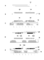
- FIG. 2 is a schematic view showing an example of a method for manufacturing a display device of the present invention.
- a sealing substrate on which a sealing agent is disposed and an element substrate on which a plurality of light emitting devices are disposed are bonded together via a surface sealing agent, and then thermally cured to manufacture a display device. It is an example.
- a sealing substrate 12 is prepared.
- the sealing substrate 12 is made of transparent glass or plastic material.
- the sealing agent 14 of the present invention is applied and formed on the sealing substrate 12 by, for example, screen printing (first step). At this time, the sealant 14 may be applied to a size that can cover the light-emitting device 18 described later.
- the sealing substrate 12 coated with the sealing agent 14 is placed on the hot plate 16 and heated. Thereby, the sealing agent 14 is heated and temporarily cured until the ball number measured according to JIS Z0237 becomes 10 or more (second step).
- an element substrate 20 on which the light emitting device 18 is arranged is prepared. Then, as shown in FIG. 2D, the sealing substrate 12 on which the sealing agent 14 is temporarily cured is bonded to the element substrate 20 and the light emitting device 18 is sealed in the sealing agent 14 (third step). . Thereafter, as shown in FIG. 2E, the sealing substrate 12 on which the sealing agent 14 is arranged is further heated and fully cured on the hot plate 16 (fourth step).
- the shape of the sealant 14 is fixed to some extent before the sealing substrate 12 and the element substrate 20 are bonded together. Therefore, when the sealing substrate 12 and the element substrate 20 are bonded together, By heating at the time of curing, it is possible to prevent the adjacent sealants 14 from sticking to each other or completely covering the terminal 18A of the light emitting device.
- sealant of the present invention can be used as both a frame sealant and a surface sealant, but is preferably used as a surface sealant suitable for the above-described display device manufacturing method. .
- the sealant of the present invention is a curable resin composition containing a curable resin as a main component.
- the curable resin refers to a resin in which polymer chains are bonded to each other by a crosslinking reaction to form a crosslinked structure.
- examples of the curable resin include phenol resin, epoxy resin, urea resin, melamine resin, unsaturated polyester resin, polyurethane, and acrylic resin. These curable resins are roughly classified into ion polymerizable compounds and radical polymerizable compounds.
- the sealant of the present invention preferably contains an ion polymerizable compound as a curable resin.
- an ion polymerizable compound as a curable resin.
- the shape of the sealing agent is maintained, and the sealing substrate and the element substrate can be bonded and adhered (adhered), preferably sealed. It is necessary to temporarily cure or dry the stopper until the ball number measured according to JIS Z0237 is 10 or more.
- An encapsulant containing only one kind of curable resin one of an ion polymerizable compound or a radical polymerizable compound reduces the storage stability of the encapsulant or the degree of cure of the encapsulant depending on the curing conditions. May be difficult to control.
- the curing conditions such as thermal curing temperature or light (such as ultraviolet rays) irradiation intensity, curing atmosphere, etc. It may be necessary to control precisely.
- the sealing agent containing two kinds of curable resins (for example, an ion polymerizable compound and a radical polymerizable compound)
- the sealing agent is used under the condition that only one of the curable resins is cured in S2 (second step). Is cured to reach a predetermined degree of curing, and then the other curable resin can be cured in S4 (fourth step). For this reason, it is possible to easily control the degree of curing in S2 (second step).
- sealing agent containing an ionic polymerizable compound and a radical polymerizable compound is used as the curable resin
- the sealing agent is subjected to radical polymerization by irradiating UV
- sealing can be performed by heating the sealing agent in S4 (fourth step) and performing ion polymerization.
- the content or molecular weight of the radically polymerizable compound and the ionic polymerizable compound contained in the sealing agent, or the addition amount of the radical polymerization initiator and the ionic polymerizable initiator are appropriately adjusted, or the reaction start temperature is adjusted.
- the curing conditions such as the thermosetting temperature in S2 (second step), the irradiation intensity of light (such as ultraviolet rays), and the curing atmosphere can be precisely determined. Even if it is not controlled, the sealant may be easily brought into a desired cured state.
- a sealing agent contains a radically polymerizable compound
- a sealing agent is arrange
- the sealing agent of the present invention contains at least (1-1) an ion polymerizable compound and (1-2) its curing agent, and (2-1) ion polymerization within one molecule as necessary. And a compound having a reactive functional group and a radical polymerizable functional group, (2-2) at least one of the radical polymerizable compound, and (2-3) a radical polymerization initiator.
- the ion polymerizable compound is a compound containing an ion polymerizable functional group such as an epoxy group.
- examples of the ion polymerizable compound include an epoxy resin, a vinyl compound containing a polar unsaturated double bond, and the like, and an epoxy resin is preferable because of low curing shrinkage.
- the epoxy resin includes a compound having one or more epoxy groups in one molecule (such as a monofunctional epoxy compound, a bifunctional epoxy compound, and a polyfunctional epoxy compound having three or more epoxy groups).
- Examples of compounds having one or more epoxy groups in one molecule include monofunctional epoxies such as phenyl glycidyl ether, 2-ethylhexyl glycidyl ether, ethyl diethylene glycol glycidyl ether, dicyclopentadiene glycidyl ether, and 2-hydroxyethyl glycidyl ether.
- monofunctional epoxies such as phenyl glycidyl ether, 2-ethylhexyl glycidyl ether, ethyl diethylene glycol glycidyl ether, dicyclopentadiene glycidyl ether, and 2-hydroxyethyl glycidyl ether.
- Curing agent for ion polymerizable compound (curing agent for epoxy resin)
- the curing agent for the ion polymerizable compound includes a latent heat curing agent and other curing agents.
- latent thermosetting agents examples include tertiary amine compounds, imidazole compounds, and amine imide compounds that are solid at room temperature.
- the latent thermosetting agent may be a material in which a tertiary amine compound or an imidazole compound is encapsulated.
- a fine powder obtained by increasing the molecular weight of a tertiary amine compound or imidazole compound is mixed with other raw materials, and the fine powdered tertiary amine compound is dissolved at the time of melt mixing by heating to cure the resin. May be.
- the other curing agent is a curing agent generally used together with the epoxy resin when the ion polymerizable compound is an epoxy resin.
- curing agents include compounds containing phenolic hydroxyl groups, polyamine compounds, polythiol compounds, acid anhydrides and the like.
- an epoxy resin sealant containing an acid anhydride as a curing agent is likely to obtain high transparency.
- acid anhydrides contained in the sealant include phthalic anhydride, tetrahydrophthalic anhydride, methyltetrahydrophthalic anhydride, trimellitic anhydride, hexachloroendomethylenetetrahydrophthalic anhydride, benzophenone tetracarboxylic anhydride, etc. It is.
- aromatic acid anhydrides are often colored, and therefore, aliphatic (aromatic hydrogenated) acid anhydrides having high transparency are preferable.
- the aliphatic acid anhydride include hexahydrophthalic anhydride and methylhexahydrophthalic anhydride.
- a compound having an ion polymerizable functional group and a radical polymerizable functional group in one molecule is composed of one or more ions. It contains a polymerizable functional group and a radically polymerizable functional group.
- the ion polymerizable functional group contained in the compound is an epoxy group, a glycidyl group, an octacenyl group or the like, and preferably an epoxy group. This is because the compatibility is good when the ion polymerizable compound is an epoxy resin.
- the radical polymerizable functional group contained in the compound is a functional group having an ethylenically unsaturated bond, such as a (meth) acryl group, a (meth) acrylamide group, a vinyl group, and preferably a (meth) acryl group. .
- the compound having an epoxy group and a radically polymerizable functional group is, for example, a vinyl monomer having an epoxy group.
- vinyl monomers having an epoxy group include (meth) acrylate monomers such as glycidyl (meth) acrylate, 3,4-epoxycyclohexylmethyl (meth) acrylate, and methyl glycidyl (meth) acrylate.
- the compound having an ion polymerizable functional group and a radical polymerizable functional group in one molecule does not contain a hydroxyl group in order to improve the storage stability of the sealant.
- an acid anhydride as a curing agent when used in combination with a compound having an ion polymerizable functional group and a radical polymerizable functional group in one molecule, when the compound contains a hydroxyl group, it reacts with the acid anhydride, This is because not only the storage stability of the sealant is lowered, but also the transparency of the resulting cured product is lowered.
- the compound having an epoxy group and a (meth) acrylate group can be obtained by, for example, (meth) acryl modification of a part of epoxy groups contained in a polyfunctional epoxy compound. Since a hydroxyl group is generated in the process of modifying this epoxy group with (meth) acryl, it is preferable to protect the generated hydroxyl group with a protecting group (for example, acylating or amidating the hydroxyl group).
- a protecting group for example, acylating or amidating the hydroxyl group.
- a radical polymerizable compound is a functional group (radical polymerizable) having an ethylenically unsaturated double bond such as (meth) acryl group, (meth) acrylamide group and vinyl group in the molecule. Functional group).
- radical polymerizable compounds examples include isobornyl (meth) acrylate, bornyl (meth) methacrylate, dicyclopentenyl (meth) acrylate, 2-hydroxyethyl (meth) acrylate, 2-hydroxypropyl (meth) acrylate, (poly ) (Meth) acrylates such as propylene glycol mono (meth) acrylate and t-butyl (meth) acrylate; (Meth) acrylamides such as morpholine (meth) acrylamide; Monofunctional radically polymerizable compounds such as N-vinylcaprolactone and styrene; Trimethylopropane tri (meth) acrylate, ethylene oxide modified trimethylolpropane tri (meth) acrylate, ethylene glycol di (meth) acrylate, diethylene glycol (meth) acrylate, triethylene glycol (meth) acrylate, tetraethylene glycol di (meth) Acrylate,
- the radical polymerization initiator includes a thermal radical polymerization initiator that generates radicals by heat and a photo radical polymerization initiator that generates radicals by light.
- Thermal radical polymerization initiators that generate radicals by heat include peroxides and azo compounds. Specific examples thereof include perbutyl O (Nippon Yushi Co., Ltd.), perbutyl D (Nippon Yushi Co., Ltd.), Luperox 575. (Arkema Yoshihiro Co., Ltd.).
- photo radical polymerization initiators that generate radicals by light include Irgacure 651 (Ciba Japan Co., Ltd.), Darocur 1173 (Ciba Japan Co., Ltd.), and the like.
- radical polymerization initiator a decomposition product when radicals are generated volatilizes as outgas, which may damage the organic EL element. For this reason, generation
- thermal radical polymerization initiators OTAZO-30 (Otsuka Chemical Co., Ltd.) has a large molecular weight of the decomposition product, has a low possibility of volatilization as outgas, and has little damage to the organic EL.
- Irgacure 2959 (Ciba Japan Co., Ltd.), Irgacure 127 (Ciba Japan Co., Ltd.) and the like have hydroxyl groups (reactive groups incorporated into the structure of the cured resin) in the molecule.
- the decomposition product after radical generation is less likely to volatilize and the organic EL element is less damaged.
- the sealing agent of the present invention may further contain a curing accelerator.
- the kind of hardening accelerator is not specifically limited, According to the kind of curable resin, it selects suitably.
- the curing accelerator may be an imidazole compound or an amine compound. Examples of the imidazole compound include 2-ethyl-4-methylimidazole, and examples of the amine compound include trisdimethylaminomethylphenol.
- the sealant of the present invention may further contain a solvent in order to adjust the viscosity.
- the sealing agent containing a solvent is obtained by diluting a curable resin composition having a high viscosity with a solvent. For this reason, in S1 (1st process) of the manufacturing method of the above-mentioned display apparatus, while improving the applicability
- the solvent is not particularly limited as long as an epoxy resin (ion polymerizable compound) or an acrylic resin (radical polymerizable compound) is easily dissolved, and methanol (boiling point 65 ° C.), ethanol (boiling point 78 ° C.), 1- Primary alcohols such as propanol (boiling point 97 ° C.), 1-butanol (boiling point 117 ° C.); secondary alcohols such as 2-propanol and 2-butanol; tertiary alcohols such as t-butanol; hydrocarbons; diethylene glycol dimethyl ether, methyl carb Ethers such as tol, ethyl carbitol and butyl carbitol; esters such as ethyl acetate; acetates such as propylene glycol diacetate, diethylene glycol diacetate and alkoxydiethylene glycol monoacetate; and methyl isobutyl ketone, methyl And ketones such as
- a solvent having a boiling point of 60 to 80 ° C. among secondary alcohols, tertiary alcohols, hydrocarbons or ethers is preferable. This is because the volatile gases of the secondary alcohol and the tertiary alcohol are extremely difficult to degrade the organic EL device (for example, they do not generate a dark spot or cause light emission) as compared with the primary alcohol.
- the solvent content in the sealant can be appropriately set so that the viscosity is easy to apply the sealant.
- fillers may further be contained in the sealing agent of this invention.
- fillers include glass beads, styrene polymer particles, methacrylate polymer particles, ethylene polymer particles, and propylene polymer particles.
- the sealing agent of the present invention may further contain various additives such as a coupling agent such as a silane coupling agent, an ion trapping agent, an ion exchange agent, a leveling agent, and an antifoaming agent, if necessary.
- a coupling agent such as a silane coupling agent, an ion trapping agent, an ion exchange agent, a leveling agent, and an antifoaming agent, if necessary.
- the sealant of the present invention contains 100 parts by mass of an epoxy resin and 0.5 to 10 parts by mass of a silane coupling agent, and further has an acid anhydride group / epoxy group equivalent ratio of 0.8 to 1.2. It is preferable that an acid anhydride is included so that the equivalent ratio of the active functional group / epoxy group of the curing accelerator is 0.008 to 0.152.
- the active functional group of the curing accelerator means an amino group or an imidazolyl group.
- the equivalent of the acid anhydride group can be obtained by dividing the molecular weight of the acid anhydride by the number of acid anhydride groups contained in one molecule of the acid anhydride.
- the equivalent of the epoxy group is obtained by dividing the molecular weight of the epoxy resin by the number of epoxy groups contained in one molecule of the epoxy resin
- the equivalent of the active functional group is the molecular weight of the curing accelerator. It is obtained by dividing by the number of active functional groups contained in one molecule of the agent.
- the sealant of the present invention preferably has a viscosity of 1.0 ⁇ 10 2 to 1.0 ⁇ 10 4 mPa ⁇ s at 25 ° C. and 1.0 rpm using an E-type viscometer. If the viscosity of the sealant is within such a range, the workability and productivity are excellent, so that the sealant can be uniformly disposed by a coating method such as screen printing. Moreover, it is because it is easy to hold
- the sealant of the present invention preferably has a water content of 100 ppm or less in order to suppress deterioration of the organic EL element.
- the amount of water contained in the sealant is determined by heating the raw material of the sealant (for example, epoxy resin) at, for example, around 100 ° C. under reduced pressure, or removing moisture in the atmosphere with a molecular sieve. It is adjusted by preparing an agent.
- the sealant of the present invention when heated at a predetermined temperature (40 to 100 ° C.), it is in an appropriate cured state. For this reason, it is preferably used in the manufacturing method of the display device of the present invention described above.
- Epoxy resin A Bisphenol F type epoxy resin (Epicron 830S manufactured by Dainippon Ink & Chemicals, Inc.)
- Epoxy resin B bisphenol A type solid epoxy resin (manufactured by JER1007 Japan Epoxy Resin)
- Curing agent Acid anhydride Tetrahydromethylphthalic anhydride (Ricacid MH700, manufactured by Shin Nippon Rika Co., Ltd.)
- Tertiary amine Trisdimethylaminomethylphenol (JER Cure 3010 manufactured by Japan Epoxy Resin Co., Ltd.)
- Modified epoxy resin A bisphenol A type epoxy resin-acrylic acid adduct (EA-1010N (hydroxyl group-containing epoxy resin), manufactured by Shin-Nakamura Chemical) Modified
- Example 1 Preparation of sealant 100 parts by weight of epoxy resin A and 97 parts by weight of tetrahydromethyl phthalic anhydride (Licacid MH700, manufactured by Shin Nippon Rika Co., Ltd.) are placed in a stirring vessel, and this is stirred and mixed at 25 ° C. for 1 hour. did. To this mixture, 2 parts by weight of ⁇ -glycidoxypropyltrimethoxysilane (KBM-403, Shin-Etsu Silicone Co., Ltd.) and 3 parts by weight of trisdimethylaminomethylphenol (JER Cure 3010, Japan Epoxy Resin Co., Ltd.) was added, and the mixture was further stirred and mixed at 25 ° C. for 0.5 hours to prepare a sealant.
- ⁇ -glycidoxypropyltrimethoxysilane KBM-403, Shin-Etsu Silicone Co., Ltd.
- JER Cure 3010 Japan Epoxy Resin Co., Ltd.
- Viscosity / Storage stability The viscosity (initial viscosity) of the prepared sealant was measured with an E-type viscometer at 25 ° C. and 1.0 rpm.
- viscosity after storing the sealant at 25 ° C. for 24 hours was measured with an E-type viscometer at 25 ° C. and 1.0 rpm.
- the ratio of the viscosity after storage to the viscosity before storage was defined as “viscosity change rate”. It shows that storage stability is so favorable that a viscosity change rate is small.
- a glass substrate was prepared as an element substrate.
- the sealant was applied to a 5 cm square print pattern by screen printing (first step). And the said glass substrate was heated for 25 minutes on the hotplate set to 80 degreeC (2nd process). The cured state of the sealant after heating was evaluated by the following (2) ball tack test. Thereafter, another glass substrate was bonded and sealed through a sealant (third step), and further heated at 80 ° C. for 95 minutes (fourth step) to obtain a display device.
- (3) shape retention and (4) visual observation of the adhesive surface were evaluated as follows.
- the cured state of the sealant after the second step in the manufacturing process of the display device was measured by the following method.
- the cured state of the sealant after the second step was measured according to “Inclined ball tack” of “Adhesive tape / adhesive sheet test method” described in JIS Z0237. That is, after the glass substrate is tilted by 20 degrees, a steel ball of a predetermined size is rolled on the sealant disposed on the glass substrate, and the steel ball stops on the sealant.
- the ball No (ball number) was measured. The larger the ball number, the better the sealant is cured without impairing the adhesion.
- the shape retention of the sealant is as follows according to the extent of the print pattern of the sealant after the fourth step with respect to the print pattern of the sealant created in the first step: evaluated.
- Spread less than 1 mm: ⁇ Spread is 1 mm or more and less than 5 mm: ⁇ Spread 5mm or more: ⁇
- Examples 2 to 3 2. A sealant was applied in the same manner as in Example 1 except that the heating time in the second step and the fourth step of the display device manufacturing method was changed as shown in Table 1.
- Examples 4 to 9 composition of sealant; The sealant was evaluated in the same manner as in Example 1 except that the heating time in the second step and the fourth step of the display device manufacturing method was changed as shown in Table 1.
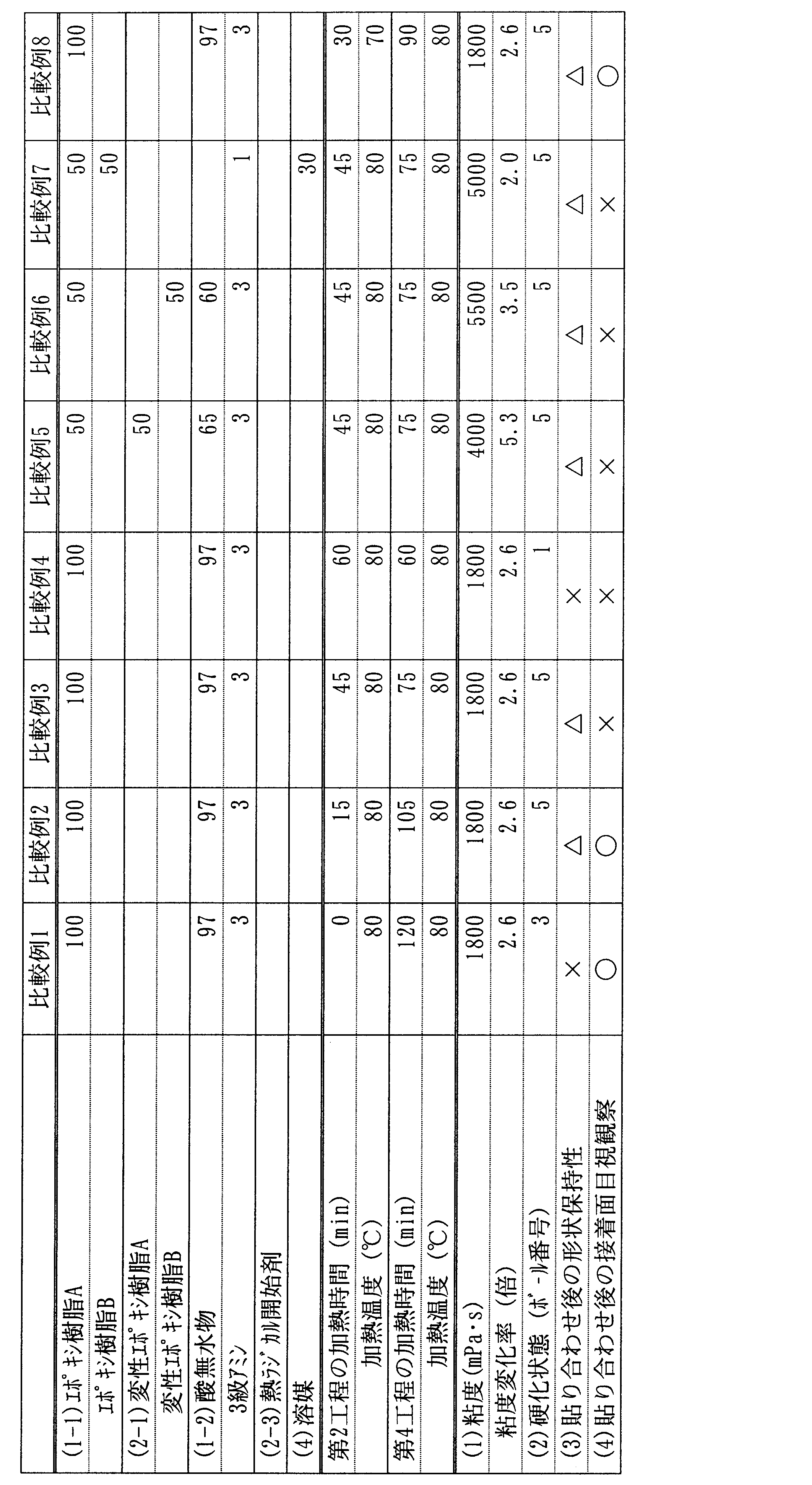
- composition of sealant The sealant was evaluated in the same manner as in Example 1 except that the heating time in the second step and the fourth step of the manufacturing method of the display device was changed as shown in Table 2.
- the ball number of the sealant can be increased to 10 or more by setting the heating time in S2 (second step) to about 15 to 40 minutes.
- all of the sealants of Examples 1 to 9 are good in both shape retention after bonding and adhesion to the substrate.
- Example 4 and Example 6 are compared, the sealing agent of Example 6 using the modified epoxy resin B not containing a hydroxyl group is the sealing agent of Example 4 using the modified epoxy resin A containing a hydroxyl group. It can be seen that the rate of change in viscosity is lower than that, and the storage stability is excellent. This is presumably because the hydroxyl group of the modified epoxy resin could be inhibited from reacting with the acid anhydride.
- a light emitting element such as an organic EL element can be sealed while maintaining the shape of the sealant.
Landscapes
- Physics & Mathematics (AREA)
- Optics & Photonics (AREA)
- Electroluminescent Light Sources (AREA)
- Sealing Material Composition (AREA)
Abstract
Description
[1]1分子内に2以上のエポキシ基を有するエポキシ樹脂と、エポキシ樹脂の硬化剤と、を含み、E型粘度計により、25℃、1.0rpmにおいて測定される粘度が1.0×10²~1.0×10⁴mPa・sであり、40~100℃のうちいずれかの温度で加熱したときの、JIS Z0237により測定されるボール番号を10以上とするための、有機EL素子の面封止剤。
[2]1分子内に2以上のエポキシ基を有するエポキシ樹脂と、エポキシ樹脂の硬化剤と、1分子内にラジカル重合性官能基とエポキシ基とを有する化合物と、ラジカル重合開始剤とを含み、E型粘度計により、25℃、1.0rpmにおいて測定される粘度が1.0×10²~1.0×10⁴mPa・sであり、40~100℃のうちいずれかの温度で加熱したとき、または100mW/cm2で30秒間光照射したときの、JIS Z0237により測定されるボール番号を10以上とするための、有機EL素子の面封止剤。
[3]2級アルコール、3級アルコール、炭化水素およびエーテル類からなる群から選ばれる少なくとも1種類の溶媒であって、沸点が60~80℃である溶媒をさらに含む、[1]または[2]記載の有機EL素子の面封止剤。
[4]前記1分子内にラジカル重合性官能基とエポキシ基とを有する化合物は、水酸基を有しておらず、かつ前記エポキシ樹脂の硬化剤は、酸無水物である、[2]または[3]記載の有機EL素子の面封止剤。
[5]前記溶媒は、2級アルコールおよび3級アルコールの少なくとも一方である、[3]または[4]記載の有機EL素子の面封止剤。
[6]水分の含有量が100ppm以下である、[1]~[5]のいずれかに記載の有機EL素子の面封止剤。
[7]前記エポキシ樹脂の硬化促進剤をさらに含み、前記硬化促進剤に含まれる活性官能基と前記面封止剤に含まれるエポキシ基の当量比が0.008~0.152であり、前記面封止剤に含まれる、酸無水基とエポキシ基の当量比が0.8~1.2である、[4]~[6]のいずれかに記載の有機EL素子の面封止剤。
[8]発光素子が配置された素子基板と前記素子基板に対向配置される封止基板とを、面封止剤を介して貼り合わせて前記発光素子を封止する表示装置の製造方法であって、(1)前記封止基板または前記素子基板の少なくとも一方に、E型粘度計により25℃、1.0rpmにおいて測定される粘度が1.0×10²~1.0×10⁴mPa・sである面封止剤を配置する第1工程と、(2)前記面封止剤を、JIS Z0237により測定されるボール番号が10以上となるまで硬化または乾燥させる第2工程と、(3)前記第2工程の後に、前記素子基板と前記封止基板とを前記面封止剤を介して貼り合わせて前記発光素子を封止する第3工程と、(4)前記面封止剤をさらに硬化させる第4工程と、を含む、表示装置の製造方法。
[9]前記面封止剤は、[1]~[7]のいずれかに記載の面封止剤である、[8]記載の表示装置の製造方法。
[10]前記発光素子は、有機EL素子である、[8]または[9]記載の表示装置の製造方法。
[11]前記第1工程において、前記面封止剤を塗布して配置する、[8]~[10]のいずれかに記載の表示装置の製造方法。
[12]前記第1工程において、前記面封止剤を前記封止基板に配置する、[8]~[11]のいずれかに記載の表示装置の製造方法。
[13]発光素子が配置された素子基板と、前記素子基板に対向配置された封止基板と、前記素子基板と、前記封止基板との間に介在し、かつ前記発光素子と前記封止基板との間に形成される空間に充填されているシール部材と、を含む表示装置であって、前記シール部材は、[1]~[7]のいずれかに記載の面封止剤の硬化物である、表示装置。
[14]前記発光素子は、有機EL素子である、[13]記載の表示装置。
本発明の表示装置は、発光素子が配置された素子基板と、素子基板と対向配置される封止基板とを有し、素子基板と封止基板は、発光素子を封止するためのシール部材を介して貼り合わされている。このシール部材は、本発明の面封止剤の硬化物である。
本発明の封止剤は、枠封止剤としても面封止剤としても用いられうるが、好ましくは前述の表示装置の製造方法に適した面封止剤として用いられる。
イオン重合性化合物は、エポキシ基などのイオン重合性官能基を含む化合物である。イオン重合性化合物の例には、エポキシ樹脂、極性を有する不飽和二重結合を含むビニル化合物などが含まれ、硬化収縮性が低いことから、好ましくはエポキシ樹脂である。
ハイドロキノンジグリシジルエーテル、レゾルシンジグリシジルエーテル、エチレングリコールジグリシジルエーテル、ポリエチレングリコールジグリシジルエーテル、1,4-ブタンジオールジグリシジルエーテル、1,6-ヘキサンジオールジグリシジルエーテル、シクロヘキサンジオールジグリシジルエーテル、シクロヘキサンジメタノールジグリシジルエーテル、ジシクロペンタジエンジオールジグリシジルエーテル、1,6-ナフタレンジオールジグリシジルエーテル、ビスフェノールAジグリシジルエーテル、ビスフェノールFジグリシジルエーテル、水添ビスフェノールAジグリシジルエーテル、水添ビスフェノールFジグリシジルエーテルなどの2官能性エポキシ化合物;
トリメチロールプロパントリグリシジルエーテル、ペンタエリスリトールテトラグリシジルエーテル、フェノールノボラック型エポキシ、クレゾールノボラック型エポキシなどの3以上の多官能性エポキシ化合物などが含まれ、好ましくは1分子内に2以上のエポキシ基を有する化合物(2官能性エポキシ化合物、3以上のエポキシ基を有する多官能性エポキシ化合物など)である。
イオン重合性化合物の硬化剤には、潜在性熱硬化剤と、その他の硬化剤とが含まれる。
1分子内にイオン重合性官能基とラジカル重合性官能基とを有する化合物は、それぞれ1以上のイオン重合性官能基と、ラジカル重合性官能基とを含む。上記化合物に含まれるイオン重合性官能基は、エポキシ基、グリシジル基、オキタセニル基などであり、好ましくはエポキシ基である。イオン重合性化合物がエポキシ樹脂である場合に、相溶性がよいためである。上記化合物に含まれるラジカル重合性官能基は、エチレン性不飽和結合を有する官能基、例えば(メタ)アクリル基、(メタ)アクリルアミド基、ビニル基などであり、好ましくは(メタ)アクリル基である。
ラジカル重合性化合物は、分子中に、(メタ)アクリル基、(メタ)アクリルアミド基およびビニル基などのエチレン性不飽和二重結合を有する官能基(ラジカル重合性官能基)を含む。
モルホリン(メタ)アクリルアミドなどの(メタ)アクリルアミド類;
N-ビニルカプロラクトン、スチレンなどの単官能性ラジカル重合性化合物;
トリメチロープロパントリ(メタ)アクリレート、エチレンオキサイド変性トリメチロールプロパントリ(メタ)アクリレート、エチレングリコールジ(メタ)アクリレート、ジエチレングリコール(メタ)アクリレート、トリエチレングリコール(メタ)アクリレート、テトラエチレングリコールジ(メタ)アクリレート、ポリエチレングリコール(メタ)アクリレート、1,4-ブタンジオールジ(メタ)アクリレート、1,6-ヘキサンジオールジ(メタ)アクリレート、ネオペンチルグリコールジ(メタ)アクリレート、ジシクロペンテニルジ(メタ)アクリレート、ジアリルフタレート、ジアリルフマレート、エチレンオキサイド変性ビスフェノールAジアクリレートなどの多官能性ラジカル重合性化合物などが含まれる。
ラジカル重合開始剤には、熱によりラジカルを発生する熱ラジカル重合開始剤と、光によりラジカルを発生する光ラジカル重合開始剤とが含まれる。
本発明の封止剤には、硬化促進剤がさらに含まれてもよい。硬化促進剤の種類は、特に限定されず、硬化性樹脂の種類に応じて適宜選択される。硬化性樹脂がエポキシ樹脂である場合、硬化促進剤は、イミダゾール化合物またはアミン化合物などでありうる。イミダゾール化合物の例には、2-エチル-4-メチルイミダゾールなどが含まれ、アミン化合物の例には、トリスジメチルアミノメチルフェノールなどが含まれる。
本発明の封止剤には、粘度を調整するために、溶媒がさらに含まれてもよい。溶媒を含む封止剤は、高粘度の硬化性樹脂組成物を溶媒で希釈して得られる。このため、前述の表示装置の製造方法のS1(第1工程)において、封止剤の塗布性を高めるとともに、S2(第2工程)において、溶媒を除去した後の封止剤を高粘度にし、形状保持性を高めることができる。
本発明の封止剤には、硬化物の機械的強度等を調整するために、任意のフィラーがさらに含まれてもよい。このようなフィラーの例には、ガラスビーズ、スチレン系ポリマー粒子、メタクリレート系ポリマー粒子、エチレン系ポリマー粒子およびプロピレン系ポリマー粒子などが含まれる。
(1-1)イオン重合性化合物
エポキシ樹脂A:ビスフェノールF型エポキシ樹脂(エピクロン830S 大日本インキ化学工業株式会社製)
エポキシ樹脂B:ビスフェノールA型固形エポキシ樹脂(JER1007 ジャパンエポキシレジン製)
(1-2)硬化剤
酸無水物:テトラヒドロメチル無水フタル酸(リカシッドMH700 新日本理化株式会社製)
3級アミン:トリスジメチルアミノメチルフェノール(JERキュア3010 ジャパンエポキシレジン株式会社製)
(2-1)ラジカル重合性官能基とエポキシ基を有する化合物(変性エポキシ樹脂)
変性エポキシ樹脂A:ビスフェノールA型エポキシ樹脂-アクリル酸付加体(EA-1010N(水酸基含有エポキシ樹脂)、新中村化学製)
変性エポキシ樹脂B:ビスフェノールA型エポキシ樹脂-フェニルメタクリレート付加体(三井化学株式会社製)
変性エポキシ樹脂Bは、以下のようにして合成した。173gのビスフェノールA型エポキシ樹脂(大日本インキ化学工業(株)製、エピクロンEXA850CRP)、162gのフェニルメタクリル酸、16gのテトラブチルアンモニウムブロマイド、および0.1gのヒドロキノンモノメチルエーテルを、攪拌機、気体導入管、温度計および冷却管を備えた500mLの4つ口フラスコ内に投入および混合し、乾燥エアにてバブリングしながら120℃、8時間加熱攪拌した。これにより、水酸基を含有しない、部分フェニエルメタクリレート化エポキシ樹脂を合成した。
(2-3)ラジカル重合開始剤
パーブチルD(日本油脂)
(4)溶媒
メチルエチルケトン(MEK)
1.封止剤の調製
100重量部のエポキシ樹脂Aと、97重量部のテトラヒドロメチル無水フタル酸(リカシッドMH700 新日本理化株式会社製)とを攪拌容器に入れ、これを25℃で1時間、撹拌混合した。この混合物に、さらに2重量部のγ-グリシドキシプロピルトリメトキシシラン(KBM-403 信越シリコーン株式会社製)と、3重量部のトリスジメチルアミノメチルフェノール(JERキュア3010 ジャパンエポキシレジン株式会社製)とを加えて、さらに25℃で0.5時間攪拌混合することにより封止剤を調製した。
調製した封止剤の粘度(初期粘度)を、E型粘度計により25℃、1.0rpmで測定した。
素子基板としてガラス基板を用意した。ガラス基板上に、封止剤を、スクリーン印刷によって5cm角の印刷パターンに塗布した(第1工程)。そして、当該ガラス基板を、80℃に設定したホットプレート上で25分間加熱した(第2工程)。加熱後の封止剤の硬化状態を、以下の(2)ボールタック試験により評価した。その後、封止剤を介して、もう1枚のガラス基板を貼り合わせて封止し(第3工程)、さらに80℃で95分間加熱して(第4工程)、表示装置を得た。得られた表示装置における、(3)形状保持性と、(4)接着面の目視観察とを以下のようにして評価した。
2.表示装置の製造過程における第2工程後の封止剤の硬化状態を、下記の方法で測定した。第2工程を行った後の封止剤の硬化状態を、JIS Z0237に記載されている「粘着テープ・粘着シート試験方法」の「傾斜式ボールタック」に準じて測定した。すなわち、ガラス基板を20度に傾けた後、該ガラス基板に配置された封止剤上に、所定の大きさの鋼球を転がして、鋼球が封止剤上で停止する、最大の大きさのボールNo(ボール番号)を測定した。ボール番号が大きいほど、封止剤が接着性を損なうことなく、良好に硬化していることを意味する。
2.表示装置の製造における、第1工程で作成した封止剤の印刷パターンに対する、第4工程を経た後の封止剤の印刷パターンの広がり具合で、封止剤の形状保持性を以下のように評価した。
広がりが1mm未満:○
広がりが1mm以上5mm未満:△
広がりが5mm以上:×
2.表示装置の製造における、第1工程で作成した封止剤の印刷パターンと比較したときの、第4工程を経た後の表示装置の封止剤の接着面の状態を目視観察し、接着状態を以下のように評価した。
封止基板と素子基板の間の封止剤の塗布パターン全域で、空洞が存在しない状態である:○
封止基板と素子基板の間の封止剤の塗布パターンの一部に、空洞が存在する:×
2.表示装置の製造方法の第2工程および第4工程における加熱時間を、表1に示されるように変更した以外は、実施例1と同様にして封止剤をした。
封止剤の組成と、2.表示装置の製造方法の第2工程および第4工程における加熱時間を、表1に示されるように変更した以外は、実施例1と同様にして封止剤を評価した。
2.表示装置の製造方法の第2工程および第4工程における加熱時間を、表2に示されるように変更した以外は、実施例1と同様にして封止剤をした。
封止剤の組成と、2.表示装置の製造方法の第2工程および第4工程における加熱時間を、表2に示されるように変更した以外は、実施例1と同様にして封止剤を評価した。

14 封止剤
16 ホットプレート
18 発光デバイス
18A 発光デバイスの端子
20 素子基板
Claims (16)
- 1分子内に2以上のエポキシ基を有するエポキシ樹脂と、
エポキシ樹脂の硬化剤と、を含み、
E型粘度計により、25℃、1.0rpmにおいて測定される粘度が1.0×10²~1.0×10⁴mPa・sであり、
40~100℃のうちいずれかの温度で加熱したときの、JIS Z0237により測定されるボール番号を10以上とするための、有機EL素子の面封止剤。 - 1分子内に2以上のエポキシ基を有するエポキシ樹脂と、
エポキシ樹脂の硬化剤と、
1分子内にラジカル重合性官能基とエポキシ基とを有する化合物と、
ラジカル重合開始剤と、を含み、
E型粘度計により、25℃、1.0rpmにおいて測定される粘度が1.0×10²~1.0×10⁴mPa・sであり、
40~100℃のうちいずれかの温度で加熱したとき、または100mW/cm2で30秒間光照射したときの、JIS Z0237により測定されるボール番号を10以上とするための、有機EL素子の面封止剤。 - 2級アルコール、3級アルコール、炭化水素およびエーテル類からなる群から選ばれる少なくとも1種類の溶媒であって、沸点が60~80℃である溶媒をさらに含む、請求項1記載の有機EL素子の面封止剤。
- 前記1分子内にラジカル重合性官能基とエポキシ基とを有する化合物は、水酸基を有しておらず、かつ前記エポキシ樹脂の硬化剤は、酸無水物である、請求項2記載の有機EL素子の面封止剤。
- 前記溶媒は、2級アルコールおよび3級アルコールの少なくとも一方である、請求項3記載の有機EL素子の面封止剤。
- 水分の含有量が100ppm以下である、請求項1記載の有機EL素子の面封止剤。
- 前記エポキシ樹脂の硬化促進剤をさらに含み、
前記硬化促進剤に含まれる活性官能基と前記面封止剤に含まれるエポキシ基の当量比が0.008~0.152であり、
前記面封止剤に含まれる、酸無水基とエポキシ基の当量比が0.8~1.2である、請求項4に記載の有機EL素子の面封止剤。 - 発光素子が配置された素子基板と前記素子基板に対向配置される封止基板とを、面封止剤を介して貼り合わせて前記発光素子を封止する表示装置の製造方法であって、
(1)前記封止基板または前記素子基板の少なくとも一方に、E型粘度計により25℃、1.0rpmにおいて測定される粘度が1.0×10²~1.0×10⁴mPa・sである面封止剤を配置する第1工程と、
(2)前記面封止剤を、JIS Z0237により測定されるボール番号が10以上となるまで硬化または乾燥させる第2工程と、
(3)前記第2工程の後に、前記素子基板と前記封止基板とを前記面封止剤を介して貼り合わせて前記発光素子を封止する第3工程と、
(4)前記面封止剤をさらに硬化させる第4工程と、を含む、表示装置の製造方法。 - 前記面封止剤は、請求項1記載の面封止剤である、請求項8記載の表示装置の製造方法。
- 前記面封止剤は、請求項2記載の面封止剤である、請求項8記載の表示装置の製造方法。
- 前記発光素子は、有機EL素子である、請求項8記載の表示装置の製造方法。
- 前記第1工程において、前記面封止剤を塗布して配置する、請求項8記載の表示装置の製造方法。
- 前記第1工程において、前記面封止剤を前記封止基板に配置する、請求項8記載の表示装置の製造方法。
- 発光素子が配置された素子基板と、
前記素子基板に対向配置された封止基板と、
前記素子基板と、前記封止基板との間に介在し、かつ前記発光素子と前記封止基板との間に形成される空間に充填されているシール部材と、を含む表示装置であって、
前記シール部材は、請求項1記載の面封止剤の硬化物である、表示装置。 - 発光素子が配置された素子基板と、
前記素子基板に対向配置された封止基板と、
前記素子基板と、前記封止基板との間に介在し、かつ前記発光素子と前記封止基板との間に形成される空間に充填されているシール部材と、を含む表示装置であって、
前記シール部材は、請求項2記載の面封止剤の硬化物である、表示装置。 - 前記発光素子は、有機EL素子である、請求項14記載の表示装置。
Priority Applications (4)
| Application Number | Priority Date | Filing Date | Title |
|---|---|---|---|
| JP2010540392A JP5639476B2 (ja) | 2008-11-28 | 2009-11-27 | 有機el素子の面封止剤、表示装置の製造方法および表示装置 |
| HK12100277.0A HK1159944B (en) | 2008-11-28 | 2009-11-27 | Organic el element surface sealant, method for producing display, and display |
| CN200980145106.8A CN102210192B (zh) | 2008-11-28 | 2009-11-27 | 有机el元件的面密封剂、显示装置的制造方法和显示装置 |
| KR1020117011782A KR101321683B1 (ko) | 2008-11-28 | 2009-11-27 | 유기 el 소자의 면 봉지제, 표시 장치의 제조방법 및 표시 장치 |
Applications Claiming Priority (2)
| Application Number | Priority Date | Filing Date | Title |
|---|---|---|---|
| JP2008303405 | 2008-11-28 | ||
| JP2008-303405 | 2008-11-28 |
Publications (1)
| Publication Number | Publication Date |
|---|---|
| WO2010061634A1 true WO2010061634A1 (ja) | 2010-06-03 |
Family
ID=42225519
Family Applications (1)
| Application Number | Title | Priority Date | Filing Date |
|---|---|---|---|
| PCT/JP2009/006448 Ceased WO2010061634A1 (ja) | 2008-11-28 | 2009-11-27 | 有機el素子の面封止剤、表示装置の製造方法および表示装置 |
Country Status (5)
| Country | Link |
|---|---|
| JP (1) | JP5639476B2 (ja) |
| KR (1) | KR101321683B1 (ja) |
| CN (1) | CN102210192B (ja) |
| TW (1) | TWI477592B (ja) |
| WO (1) | WO2010061634A1 (ja) |
Cited By (11)
| Publication number | Priority date | Publication date | Assignee | Title |
|---|---|---|---|---|
| JP2013121702A (ja) * | 2011-12-12 | 2013-06-20 | Fujifilm Corp | バリア性積層体、ガスバリアフィルムおよびこれらを用いたデバイス |
| CN103317816A (zh) * | 2012-03-23 | 2013-09-25 | 芝浦机械电子装置股份有限公司 | 粘合装置以及粘合方法 |
| JP2014044943A (ja) * | 2012-07-30 | 2014-03-13 | Mitsubishi Plastics Inc | 捕水剤、それを用いた有機電子デバイス及び有機elデバイス |
| JP2015529934A (ja) * | 2012-06-29 | 2015-10-08 | テーザ・ソシエタス・ヨーロピア | 有機電子的装置をカプセル化するための接着テープ |
| WO2016167347A1 (ja) * | 2015-04-17 | 2016-10-20 | 積水化学工業株式会社 | 電子デバイス用封止剤及び電子デバイスの製造方法 |
| WO2017051795A1 (ja) * | 2015-09-24 | 2017-03-30 | 積水化学工業株式会社 | 電子デバイス用封止剤及び電子デバイスの製造方法 |
| WO2019181592A1 (ja) * | 2018-03-19 | 2019-09-26 | 三井化学株式会社 | 表示素子用封止材およびその硬化物、有機el素子用枠封止材、ならびに有機el素子用面封止材 |
| JP2020034867A (ja) * | 2018-08-31 | 2020-03-05 | 三井化学株式会社 | 硬化型封止材、硬化物および表示装置 |
| JPWO2021131790A1 (ja) * | 2019-12-27 | 2021-07-01 | ||
| US11078324B2 (en) * | 2016-10-28 | 2021-08-03 | Sharp Kabushiki Kaisha | Seal material composition, liquid crystal cell, and scanned antenna |
| WO2022085599A1 (ja) * | 2020-10-20 | 2022-04-28 | デンカ株式会社 | 封止剤、硬化体、有機エレクトロルミネッセンス表示装置、及び、有機エレクトロルミネッセンス表示装置の製造方法 |
Families Citing this family (4)
| Publication number | Priority date | Publication date | Assignee | Title |
|---|---|---|---|---|
| KR101404361B1 (ko) * | 2011-11-14 | 2014-06-09 | 주식회사 엘지화학 | 접착 필름 및 이를 이용한 유기전자장치의 봉지 방법 |
| KR102156765B1 (ko) * | 2013-12-13 | 2020-09-16 | 엘지디스플레이 주식회사 | 유기 발광 표시 장치 및 이의 제조 방법 |
| JP6235907B2 (ja) * | 2014-01-07 | 2017-11-22 | 芝浦メカトロニクス株式会社 | 基板貼合装置、表示装置用部材の製造装置及び表示装置用部材の製造方法 |
| JP6827526B2 (ja) | 2016-12-09 | 2021-02-10 | エルジー・ケム・リミテッド | 密封材組成物 |
Citations (7)
| Publication number | Priority date | Publication date | Assignee | Title |
|---|---|---|---|---|
| JP2000068050A (ja) * | 1998-08-24 | 2000-03-03 | Casio Comput Co Ltd | 電界発光素子及びその製造方法 |
| JP2003197366A (ja) * | 2001-12-25 | 2003-07-11 | Sanyo Electric Co Ltd | 表示装置及びその製造方法 |
| JP2003203762A (ja) * | 2001-11-01 | 2003-07-18 | Sony Corp | 表示装置 |
| JP2006113203A (ja) * | 2004-10-13 | 2006-04-27 | Nitto Denko Corp | 積層光学フィルム、楕円偏光板および画像表示装置 |
| JP2006228708A (ja) * | 2005-01-20 | 2006-08-31 | Mitsui Chemicals Inc | 有機elシール材 |
| JP2006236987A (ja) * | 2005-01-26 | 2006-09-07 | Sekisui Chem Co Ltd | 有機エレクトロルミネッセンス素子用封止剤、有機エレクトロルミネッセンス素子の封止方法及び有機エレクトロルミネッセンス素子 |
| WO2007040209A1 (ja) * | 2005-10-03 | 2007-04-12 | Mitsui Chemicals, Inc. | フラットパネルディスプレイ用シール材 |
-
2009
- 2009-11-27 KR KR1020117011782A patent/KR101321683B1/ko active Active
- 2009-11-27 TW TW098140636A patent/TWI477592B/zh active
- 2009-11-27 JP JP2010540392A patent/JP5639476B2/ja active Active
- 2009-11-27 WO PCT/JP2009/006448 patent/WO2010061634A1/ja not_active Ceased
- 2009-11-27 CN CN200980145106.8A patent/CN102210192B/zh active Active
Patent Citations (7)
| Publication number | Priority date | Publication date | Assignee | Title |
|---|---|---|---|---|
| JP2000068050A (ja) * | 1998-08-24 | 2000-03-03 | Casio Comput Co Ltd | 電界発光素子及びその製造方法 |
| JP2003203762A (ja) * | 2001-11-01 | 2003-07-18 | Sony Corp | 表示装置 |
| JP2003197366A (ja) * | 2001-12-25 | 2003-07-11 | Sanyo Electric Co Ltd | 表示装置及びその製造方法 |
| JP2006113203A (ja) * | 2004-10-13 | 2006-04-27 | Nitto Denko Corp | 積層光学フィルム、楕円偏光板および画像表示装置 |
| JP2006228708A (ja) * | 2005-01-20 | 2006-08-31 | Mitsui Chemicals Inc | 有機elシール材 |
| JP2006236987A (ja) * | 2005-01-26 | 2006-09-07 | Sekisui Chem Co Ltd | 有機エレクトロルミネッセンス素子用封止剤、有機エレクトロルミネッセンス素子の封止方法及び有機エレクトロルミネッセンス素子 |
| WO2007040209A1 (ja) * | 2005-10-03 | 2007-04-12 | Mitsui Chemicals, Inc. | フラットパネルディスプレイ用シール材 |
Cited By (21)
| Publication number | Priority date | Publication date | Assignee | Title |
|---|---|---|---|---|
| JP2013121702A (ja) * | 2011-12-12 | 2013-06-20 | Fujifilm Corp | バリア性積層体、ガスバリアフィルムおよびこれらを用いたデバイス |
| CN103317816A (zh) * | 2012-03-23 | 2013-09-25 | 芝浦机械电子装置股份有限公司 | 粘合装置以及粘合方法 |
| CN103317816B (zh) * | 2012-03-23 | 2017-07-21 | 芝浦机械电子装置股份有限公司 | 粘合装置以及粘合基板的制造方法 |
| JP2015529934A (ja) * | 2012-06-29 | 2015-10-08 | テーザ・ソシエタス・ヨーロピア | 有機電子的装置をカプセル化するための接着テープ |
| JP2014044943A (ja) * | 2012-07-30 | 2014-03-13 | Mitsubishi Plastics Inc | 捕水剤、それを用いた有機電子デバイス及び有機elデバイス |
| WO2016167347A1 (ja) * | 2015-04-17 | 2016-10-20 | 積水化学工業株式会社 | 電子デバイス用封止剤及び電子デバイスの製造方法 |
| WO2017051795A1 (ja) * | 2015-09-24 | 2017-03-30 | 積水化学工業株式会社 | 電子デバイス用封止剤及び電子デバイスの製造方法 |
| JPWO2017051795A1 (ja) * | 2015-09-24 | 2018-07-12 | 積水化学工業株式会社 | 電子デバイス用封止剤及び電子デバイスの製造方法 |
| US11078324B2 (en) * | 2016-10-28 | 2021-08-03 | Sharp Kabushiki Kaisha | Seal material composition, liquid crystal cell, and scanned antenna |
| CN111886315A (zh) * | 2018-03-19 | 2020-11-03 | 三井化学株式会社 | 显示元件用密封材及其固化物、有机el元件用框密封材以及有机el元件用面密封材 |
| JPWO2019181592A1 (ja) * | 2018-03-19 | 2020-12-03 | 三井化学株式会社 | 表示素子用封止材およびその硬化物、有機el素子用枠封止材、ならびに有機el素子用面封止材 |
| WO2019181592A1 (ja) * | 2018-03-19 | 2019-09-26 | 三井化学株式会社 | 表示素子用封止材およびその硬化物、有機el素子用枠封止材、ならびに有機el素子用面封止材 |
| CN111886315B (zh) * | 2018-03-19 | 2023-06-30 | 三井化学株式会社 | 显示元件用密封材及其固化物、有机el元件用框密封材以及有机el元件用面密封材 |
| JP2020034867A (ja) * | 2018-08-31 | 2020-03-05 | 三井化学株式会社 | 硬化型封止材、硬化物および表示装置 |
| JP7182958B2 (ja) | 2018-08-31 | 2022-12-05 | 三井化学株式会社 | 硬化型封止材、硬化物および表示装置 |
| JPWO2021131790A1 (ja) * | 2019-12-27 | 2021-07-01 | ||
| CN114902804A (zh) * | 2019-12-27 | 2022-08-12 | 三井化学株式会社 | 固化性组合物及有机el显示装置 |
| WO2022085599A1 (ja) * | 2020-10-20 | 2022-04-28 | デンカ株式会社 | 封止剤、硬化体、有機エレクトロルミネッセンス表示装置、及び、有機エレクトロルミネッセンス表示装置の製造方法 |
| JPWO2022085599A1 (ja) * | 2020-10-20 | 2022-04-28 | ||
| CN116194508A (zh) * | 2020-10-20 | 2023-05-30 | 电化株式会社 | 密封剂、固化体、有机电致发光显示装置及有机电致发光显示装置的制造方法 |
| JP7523568B2 (ja) | 2020-10-20 | 2024-07-26 | デンカ株式会社 | 封止剤、硬化体、有機エレクトロルミネッセンス表示装置、及び、有機エレクトロルミネッセンス表示装置の製造方法 |
Also Published As
| Publication number | Publication date |
|---|---|
| JP5639476B2 (ja) | 2014-12-10 |
| CN102210192B (zh) | 2014-07-30 |
| JPWO2010061634A1 (ja) | 2012-04-26 |
| TWI477592B (zh) | 2015-03-21 |
| TW201030133A (en) | 2010-08-16 |
| KR20110090947A (ko) | 2011-08-10 |
| KR101321683B1 (ko) | 2013-10-23 |
| HK1159944A1 (en) | 2012-08-03 |
| CN102210192A (zh) | 2011-10-05 |
Similar Documents
| Publication | Publication Date | Title |
|---|---|---|
| JP5639476B2 (ja) | 有機el素子の面封止剤、表示装置の製造方法および表示装置 | |
| JP6200591B2 (ja) | インクジェット塗布用電子デバイス用封止剤及び電子デバイスの製造方法 | |
| JP6997062B2 (ja) | 有機el表示素子用封止剤及び有機el表示素子用封止剤の製造方法 | |
| JP2014225380A (ja) | 有機エレクトロルミネッセンス表示素子用封止剤及び有機エレクトロルミネッセンス表示素子の製造方法 | |
| JP6985228B2 (ja) | 有機el表示素子用封止剤 | |
| JP6014325B2 (ja) | 有機エレクトロルミネッセンス表示素子用封止剤 | |
| WO2013027389A1 (ja) | シート状エポキシ樹脂組成物、及びこれを含む封止用シート | |
| JP6247125B2 (ja) | 有機光デバイスの製造方法 | |
| JPWO2017051795A1 (ja) | 電子デバイス用封止剤及び電子デバイスの製造方法 | |
| JP2022027778A (ja) | 有機el表示素子用封止剤 | |
| JP6793471B2 (ja) | 液晶滴下工法用シール材、液晶表示パネル及び液晶表示パネルの製造方法 | |
| JP2012129010A (ja) | 有機エレクトロルミネッセンス表示素子用封止剤 | |
| JP5597338B2 (ja) | 液晶表示パネルの製造方法およびそのシール剤 | |
| CN113166371B (zh) | 有机el显示元件用密封剂 | |
| JP2022087332A (ja) | 有機el表示素子用封止剤 | |
| HK1159944B (en) | Organic el element surface sealant, method for producing display, and display | |
| TW202444827A (zh) | 硬化性組成物、密封劑、框密封劑、顯示面板及其製造方法 | |
| JP2016017175A (ja) | 表示素子用保護剤 | |
| CN112074957A (zh) | 有机el显示元件用密封剂 | |
| CN111972046A (zh) | 有机el显示元件用密封剂 | |
| JP2011028396A (ja) | タッチパネル装置の製造方法及びタッチパネル装置 |
Legal Events
| Date | Code | Title | Description |
|---|---|---|---|
| WWE | Wipo information: entry into national phase |
Ref document number: 200980145106.8 Country of ref document: CN |
|
| 121 | Ep: the epo has been informed by wipo that ep was designated in this application |
Ref document number: 09828884 Country of ref document: EP Kind code of ref document: A1 |
|
| ENP | Entry into the national phase |
Ref document number: 2010540392 Country of ref document: JP Kind code of ref document: A |
|
| ENP | Entry into the national phase |
Ref document number: 20117011782 Country of ref document: KR Kind code of ref document: A |
|
| NENP | Non-entry into the national phase |
Ref country code: DE |
|
| 122 | Ep: pct application non-entry in european phase |
Ref document number: 09828884 Country of ref document: EP Kind code of ref document: A1 |