WO2010038542A1 - 光半導体装置 - Google Patents
光半導体装置 Download PDFInfo
- Publication number
- WO2010038542A1 WO2010038542A1 PCT/JP2009/063598 JP2009063598W WO2010038542A1 WO 2010038542 A1 WO2010038542 A1 WO 2010038542A1 JP 2009063598 W JP2009063598 W JP 2009063598W WO 2010038542 A1 WO2010038542 A1 WO 2010038542A1
- Authority
- WO
- WIPO (PCT)
- Prior art keywords
- quantum dot
- layer
- active layer
- density
- layers
- Prior art date
- Legal status (The legal status is an assumption and is not a legal conclusion. Google has not performed a legal analysis and makes no representation as to the accuracy of the status listed.)
- Ceased
Links
Images

Classifications
-
- H—ELECTRICITY
- H01—ELECTRIC ELEMENTS
- H01S—DEVICES USING THE PROCESS OF LIGHT AMPLIFICATION BY STIMULATED EMISSION OF RADIATION [LASER] TO AMPLIFY OR GENERATE LIGHT; DEVICES USING STIMULATED EMISSION OF ELECTROMAGNETIC RADIATION IN WAVE RANGES OTHER THAN OPTICAL
- H01S5/00—Semiconductor lasers
- H01S5/30—Structure or shape of the active region; Materials used for the active region
- H01S5/34—Structure or shape of the active region; Materials used for the active region comprising quantum well or superlattice structures, e.g. single quantum well [SQW] lasers, multiple quantum well [MQW] lasers or graded index separate confinement heterostructure [GRINSCH] lasers
- H01S5/341—Structures having reduced dimensionality, e.g. quantum wires
-
- B—PERFORMING OPERATIONS; TRANSPORTING
- B82—NANOTECHNOLOGY
- B82Y—SPECIFIC USES OR APPLICATIONS OF NANOSTRUCTURES; MEASUREMENT OR ANALYSIS OF NANOSTRUCTURES; MANUFACTURE OR TREATMENT OF NANOSTRUCTURES
- B82Y20/00—Nanooptics, e.g. quantum optics or photonic crystals
-
- H—ELECTRICITY
- H01—ELECTRIC ELEMENTS
- H01S—DEVICES USING THE PROCESS OF LIGHT AMPLIFICATION BY STIMULATED EMISSION OF RADIATION [LASER] TO AMPLIFY OR GENERATE LIGHT; DEVICES USING STIMULATED EMISSION OF ELECTROMAGNETIC RADIATION IN WAVE RANGES OTHER THAN OPTICAL
- H01S5/00—Semiconductor lasers
- H01S5/10—Construction or shape of the optical resonator, e.g. extended or external cavity, coupled cavities, bent-guide, varying width, thickness or composition of the active region
-
- H—ELECTRICITY
- H01—ELECTRIC ELEMENTS
- H01S—DEVICES USING THE PROCESS OF LIGHT AMPLIFICATION BY STIMULATED EMISSION OF RADIATION [LASER] TO AMPLIFY OR GENERATE LIGHT; DEVICES USING STIMULATED EMISSION OF ELECTROMAGNETIC RADIATION IN WAVE RANGES OTHER THAN OPTICAL
- H01S5/00—Semiconductor lasers
- H01S5/10—Construction or shape of the optical resonator, e.g. extended or external cavity, coupled cavities, bent-guide, varying width, thickness or composition of the active region
- H01S5/1053—Comprising an active region having a varying composition or cross-section in a specific direction
-
- H—ELECTRICITY
- H01—ELECTRIC ELEMENTS
- H01S—DEVICES USING THE PROCESS OF LIGHT AMPLIFICATION BY STIMULATED EMISSION OF RADIATION [LASER] TO AMPLIFY OR GENERATE LIGHT; DEVICES USING STIMULATED EMISSION OF ELECTROMAGNETIC RADIATION IN WAVE RANGES OTHER THAN OPTICAL
- H01S5/00—Semiconductor lasers
- H01S5/20—Structure or shape of the semiconductor body to guide the optical wave ; Confining structures perpendicular to the optical axis, e.g. index or gain guiding, stripe geometry, broad area lasers, gain tailoring, transverse or lateral reflectors, special cladding structures, MQW barrier reflection layers
- H01S5/22—Structure or shape of the semiconductor body to guide the optical wave ; Confining structures perpendicular to the optical axis, e.g. index or gain guiding, stripe geometry, broad area lasers, gain tailoring, transverse or lateral reflectors, special cladding structures, MQW barrier reflection layers having a ridge or stripe structure
-
- H—ELECTRICITY
- H01—ELECTRIC ELEMENTS
- H01S—DEVICES USING THE PROCESS OF LIGHT AMPLIFICATION BY STIMULATED EMISSION OF RADIATION [LASER] TO AMPLIFY OR GENERATE LIGHT; DEVICES USING STIMULATED EMISSION OF ELECTROMAGNETIC RADIATION IN WAVE RANGES OTHER THAN OPTICAL
- H01S5/00—Semiconductor lasers
- H01S5/30—Structure or shape of the active region; Materials used for the active region
- H01S5/34—Structure or shape of the active region; Materials used for the active region comprising quantum well or superlattice structures, e.g. single quantum well [SQW] lasers, multiple quantum well [MQW] lasers or graded index separate confinement heterostructure [GRINSCH] lasers
- H01S5/341—Structures having reduced dimensionality, e.g. quantum wires
- H01S5/3412—Structures having reduced dimensionality, e.g. quantum wires quantum box or quantum dash
Definitions
- the present invention relates to an optical semiconductor device, and more particularly to an optical semiconductor device in which an active layer has a plurality of quantum dots.
- Patent Document 1 discloses a method for forming quantum dots.
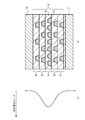
- FIG. 1A is a schematic cross-sectional view of a conventional semiconductor laser, and FIG. 1B shows a waveguide mode of light in the semiconductor laser.
- an active layer 14 is provided on a lower cladding layer 12 having a first conductivity type.
- the active layer 14 includes a plurality of stacked quantum dot layers 51 to 55.
- the quantum dot layers 51 to 55 include a plurality of quantum dots 41 and a base layer 40 that covers the quantum dots 41.
- the quantum dot density (quantum dot surface density) in each of the quantum dot layers 51 to 55 is the same.
- An upper cladding layer 18 having a second conductivity type (conductivity type opposite to the first conductivity type) is provided on the active layer 14.
- the quantum dots 41 in the active layer 14 emit light, and the emitted light propagates in the active layer 14.
- the refractive indexes of the lower cladding layer 12 and the upper cladding layer 18 are lower than the refractive index of the base layer 40 that mainly constitutes the active layer 14. For this reason, the waveguide mode of light propagating in the vicinity of the active layer 14 is greatest near the center of the active layer 14 as shown in FIG.
- the quantum dot density in order to increase the device current and increase the light output intensity.
- the quantum dot density in order to increase the interaction between light and current and improve the light modulation efficiency.
- crystal distortion increases and dislocations that become non-luminescent centers increase. Therefore, the light emission efficiency and the modulation efficiency are reduced.
- the present invention has been made in view of the above problems, and an object thereof is to improve the efficiency of an optical semiconductor device having quantum dots.
- the present invention includes a lower cladding layer having a first conductivity type, an active layer provided on the lower cladding layer, in which a plurality of quantum dot layers having a plurality of quantum dots are stacked, and provided on the active layer, And an upper cladding layer having a second conductivity type opposite to the first conductivity type, wherein the plurality of quantum dot layers have different quantum dot densities. is there.
- the efficiency of the optical semiconductor device can be improved.
- the plurality of quantum dot layers have a quantum dot density of a quantum dot layer having a large waveguide mode of light propagating through the active layer and a quantum dot density of a quantum dot layer having a small waveguide mode of light.
- the quantum dot density can be different from each other so as to be low. According to this configuration, the efficiency of the optical semiconductor device can be improved by varying the quantum dot density according to the size of the waveguide mode of light.
- the plurality of quantum dot layers can be configured such that the quantum dot density monotonously decreases from the quantum dot layer having the highest quantum dot density toward the quantum dot layer at the end of the active layer.
- the quantum dot density of the quantum dot layer at the center of the active layer among the plurality of quantum dot layers may be higher than the quantum dot layers above and below the active layer.
- the uppermost quantum dot among the plurality of quantum dot layers may have the highest density.
- a light guide layer having a refractive index larger than that of the lower clad layer and the upper clad layer may be provided on the active layer.
- the efficiency of the optical semiconductor device can be improved.
- FIG. 1A is a schematic cross-sectional view of a conventional semiconductor laser
- FIG. 1B is a diagram showing a waveguide mode of light in the semiconductor laser
- FIG. 2A is a schematic cross-sectional view of the semiconductor laser according to the first embodiment
- FIG. 2B is a diagram illustrating a waveguide mode of light in the semiconductor laser
- FIG. 3A is a schematic cross-sectional view of the semiconductor laser according to the first embodiment
- FIG. 3B is a diagram illustrating a waveguide mode of light in the semiconductor laser.
- FIG. 4 is a cross-sectional perspective view of the semiconductor laser according to the third embodiment.
- FIG. 5 is a diagram showing a dot layer for one quantum dot active layer.
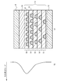
- FIG. 2A is a schematic cross-sectional view of the semiconductor laser according to the first embodiment, and FIG. 2B shows a waveguide mode of light in the semiconductor laser.
- the quantum dot density (surface density of the quantum dots) of the quantum dot layer 53 in the central portion where the light waveguide mode is the highest is the highest.
- the quantum dot density of the uppermost and lowermost quantum dot layers 51 and 55 having the smallest optical waveguide mode is the lowest.
- the quantum dot density monotonously decreases from the quantum dot layer 53 to the quantum dot layers 51 and 55.
- the quantum dot density of the quantum dot layer 53 at the center of the active layer 14 among the plurality of quantum dot layers 51 to 55 is made higher than the quantum dot layers 51 and 55 above and below the active layer 14.
- the active layer 14 emits light efficiently in the central region of the active layer 14 having a large light guiding mode. Therefore, the light emission efficiency of the semiconductor laser can be improved.
- the total number of quantum dots 41 in the active layer 14 substantially the same as that of the conventional semiconductor laser of FIG. it can. Therefore, the dislocation density causing the non-radiative center can be set to the same level as the conventional one.
- the waveguide mode of light is almost symmetrical vertically. Therefore, it is preferable that the quantum dot density is substantially symmetrical up and down.
- Example 2 is an example in which the uppermost quantum dot layer has the highest quantum dot density.
- FIG. 3A is a schematic cross-sectional view of a semiconductor laser according to the second embodiment, and FIG. 3B shows a waveguide mode of light in the semiconductor laser.
- a light guide layer 58 is provided on the active layer 14 as compared with FIG. 2A of the first embodiment.
- the light guide layer 58 is a layer having a higher refractive index than the upper cladding layer 18 and the lower cladding layer 12.
- the light guide layer 58 has a function of propagating light. Therefore, as shown in FIG. 3B, the light waveguide mode increases near the center of the active layer 14 and the light guide layer 58. If attention is paid to the active layer 14, the waveguide mode of light increases above the active layer 14. Therefore, the quantum dot density of the uppermost quantum dot layer 55 among the plurality of quantum dot layers is made highest. The quantum dot density of the lowest quantum dot layer 51 is made the lowest. The quantum dot density is monotonously decreased from the quantum dot layer 55 to the quantum dot layer 51. Thereby, the active layer 14 emits light efficiently in the upper region of the active layer 14 having a large light guiding mode. Therefore, the light emission efficiency of the semiconductor laser can be improved.
- the quantum dot density of the quantum dot layer having a large waveguide mode of light propagating through the active layer is high and the quantum dot density of the quantum dot layer having a small waveguide mode of light is
- the quantum dot densities of the plurality of quantum dot layers 51 to 55 are made different so as to be lowered. Thereby, the light emission efficiency of the semiconductor laser can be improved.
- the quantum dot density of the lowermost quantum dot layer 51 is increased.
- the highest quantum dot layer 55 can have the lowest quantum dot density.
- the waveguide mode of light generally has one peak and decreases monotonously up and down. Therefore, it is preferable that the quantum dot layers 51 to 55 monotonically decrease from the quantum dot layer having the highest quantum dot density toward the quantum dot layer 51 or 55 at the end of the active layer 14.
- the five quantum dot layers 51 to 55 are described as an example.
- the quantum dot layer may be six layers or more, for example, ten layers or more.
- the size of the quantum dot is about 20 nm in diameter, for example.
- the quantum dot density of the quantum dot layer having a large quantum dot density is, for example, 6 ⁇ 10 10 pieces / cm 2
- the quantum dot density of the quantum dot layer having a small quantum dot density is, for example, 1 ⁇ 10 10 pieces / cm 2 .
- the maximum quantum dot density is preferably 1.2 times or more with respect to the minimum quantum dot density in the quantum dot layers 51 to 55. 5 times or more is more preferable. Furthermore, 3.0 times or more is more preferable.
- Example 1 and Example 2 are examples of a semiconductor laser, but Example 1 and Example 2 may be used for a semiconductor optical amplifier. Thereby, the interaction between light and current in the semiconductor optical amplifier can be increased, and the light modulation efficiency can be improved.
- Example 3 is an example of a semiconductor laser using Example 1 and Example 2.
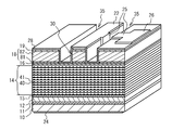
- FIG. 4 is a cross-sectional perspective view of the third embodiment.
- a buffer layer 11 made of p-type GaAs
- a lower cladding layer 12 made of p-type AlGaAs
- a spacer layer 15 made of undoped GaAs
- a quantum dot active layer 14 in which a plurality of quantum dot layers are stacked, an undoped GaAs
- a spacer layer 16 made of, an upper clad layer 18 made of n-type AlGaAs, and a contact layer 19 made of n-type GaAs are sequentially stacked.
- the active layer 14 includes quantum dots 41 and a base layer 40.
- the upper cladding layer 18 includes a first layer 81 and a second layer 82.
- the density of the quantum dots 41 is illustrated in the same manner between the quantum dot layers, but the quantum dot density is different between the quantum dot layers as in the first and second embodiments.
- Table 1 shows the material, film thickness, and doping concentration of each layer.
- the upper cladding layer 18 and the contact layer 19 form a ridge portion 30. Concave portions 35 reaching the spacer layer 16 are formed on both sides of the ridge portion 30.
- a silicon oxide film is formed as a protective film 28 on the contact layer 19 and on the surface of the recess 35.
- An n electrode 22 is formed on the contact layer 19 of the ridge 30.
- a pad 26 connected to the n electrode 22 via the wiring 25 is formed.
- a p-electrode 24 is formed on the lower surface of the substrate 10.
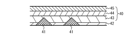
- FIG. 5 is a diagram showing a quantum dot layer for one quantum dot active layer.
- the quantum dots 41 are made of InAs.
- An InGaAs layer 42 having a thickness of about 5 nm is formed between the quantum dots 41.
- An undoped GaAs layer 43 having a thickness of about 14 nm is formed so as to cover the quantum dots 41 and the InGaAs layer 42.
- a p-type GaAs layer 44 having a thickness of about 10 nm and an undoped GaAs layer 45 having a thickness of 9 nm are formed on the undoped GaAs layer 43.
- the undoped GaAs layer 43, the p-type GaAs layer 44, and the undoped GaAs layer 45 constitute a base layer 40.
- Table 2 shows the material, film thickness, and doping concentration of each layer in the quantum dot active layer 14.
- InAs can be used as the quantum dots 41
- GaAs can be used as the base layer 40
- AlGaAs can be used as the lower cladding layer 12 and the upper cladding layer 18.
- GaAs can be used as the light guide layer.
Landscapes
- Physics & Mathematics (AREA)
- Optics & Photonics (AREA)
- Chemical & Material Sciences (AREA)
- Engineering & Computer Science (AREA)
- Nanotechnology (AREA)
- Condensed Matter Physics & Semiconductors (AREA)
- General Physics & Mathematics (AREA)
- Electromagnetism (AREA)
- Life Sciences & Earth Sciences (AREA)
- Biophysics (AREA)
- Crystallography & Structural Chemistry (AREA)
- Semiconductor Lasers (AREA)
Priority Applications (2)
| Application Number | Priority Date | Filing Date | Title |
|---|---|---|---|
| US13/121,528 US8625193B2 (en) | 2008-10-01 | 2009-07-30 | Optical semiconductor device |
| CN2009801388365A CN102171898A (zh) | 2008-10-01 | 2009-07-30 | 光半导体装置 |
Applications Claiming Priority (2)
| Application Number | Priority Date | Filing Date | Title |
|---|---|---|---|
| JP2008256013A JP5303236B2 (ja) | 2008-10-01 | 2008-10-01 | 光半導体装置 |
| JP2008-256013 | 2008-10-01 |
Publications (1)
| Publication Number | Publication Date |
|---|---|
| WO2010038542A1 true WO2010038542A1 (ja) | 2010-04-08 |
Family
ID=42073319
Family Applications (1)
| Application Number | Title | Priority Date | Filing Date |
|---|---|---|---|
| PCT/JP2009/063598 Ceased WO2010038542A1 (ja) | 2008-10-01 | 2009-07-30 | 光半導体装置 |
Country Status (4)
| Country | Link |
|---|---|
| US (1) | US8625193B2 (cg-RX-API-DMAC7.html) |
| JP (1) | JP5303236B2 (cg-RX-API-DMAC7.html) |
| CN (1) | CN102171898A (cg-RX-API-DMAC7.html) |
| WO (1) | WO2010038542A1 (cg-RX-API-DMAC7.html) |
Families Citing this family (5)
| Publication number | Priority date | Publication date | Assignee | Title |
|---|---|---|---|---|
| JP6601791B2 (ja) * | 2015-07-13 | 2019-11-06 | 株式会社Qdレーザ | 半導体レーザ、光モジュール、光通信装置、及び光通信システム |
| US10840676B2 (en) * | 2018-05-10 | 2020-11-17 | X Development Llc | Optoelectronic devices having spatially varying distribution of quantum confined nanostructures |
| CN114389150B (zh) * | 2020-10-05 | 2025-12-26 | 新科实业有限公司 | 光源单元、热辅助磁头、头万向节总成和硬盘驱动器 |
| JP7543862B2 (ja) * | 2020-11-13 | 2024-09-03 | 株式会社デンソー | 半導体レーザ装置 |
| JP7619195B2 (ja) * | 2021-07-13 | 2025-01-22 | 株式会社デンソー | 光半導体素子 |
Citations (5)
| Publication number | Priority date | Publication date | Assignee | Title |
|---|---|---|---|---|
| JPH05145183A (ja) * | 1991-11-19 | 1993-06-11 | Fujitsu Ltd | 半導体発光装置 |
| JPH11307860A (ja) * | 1998-04-17 | 1999-11-05 | Nec Corp | 半導体レーザ及び半導体光アンプ |
| JP2003309322A (ja) * | 2002-04-16 | 2003-10-31 | Fujitsu Ltd | 自己形成量子ドットを用いた半導体発光素子 |
| WO2004055900A1 (ja) * | 2002-12-16 | 2004-07-01 | Japan Science And Technology Agency | 不均一な量子ドットを有する半導体積層構造、それを用いた発光ダイオード、半導体レーザダイオード及び半導体光増幅器並びにそれらの製造方法 |
| JP2005268573A (ja) * | 2004-03-19 | 2005-09-29 | Fujitsu Ltd | 自己形成型量子ドットを用いた半導体発光素子 |
Family Cites Families (6)
| Publication number | Priority date | Publication date | Assignee | Title |
|---|---|---|---|---|
| JP3468866B2 (ja) | 1994-09-16 | 2003-11-17 | 富士通株式会社 | 3次元量子閉じ込めを利用した半導体装置 |
| JP2001210910A (ja) | 1999-11-17 | 2001-08-03 | Mitsubishi Electric Corp | 半導体レーザ |
| JP2004289010A (ja) * | 2003-03-24 | 2004-10-14 | Sony Corp | 発光装置 |
| JP2005039107A (ja) * | 2003-07-17 | 2005-02-10 | Sharp Corp | 酸化物半導体レーザ素子 |
| JP2008098299A (ja) * | 2006-10-10 | 2008-04-24 | Mitsubishi Electric Corp | 半導体光素子及びその製造方法 |
| JP5145183B2 (ja) | 2008-09-26 | 2013-02-13 | 日本電産サンキョー株式会社 | 扉ロック装置 |
-
2008
- 2008-10-01 JP JP2008256013A patent/JP5303236B2/ja active Active
-
2009
- 2009-07-30 CN CN2009801388365A patent/CN102171898A/zh active Pending
- 2009-07-30 US US13/121,528 patent/US8625193B2/en not_active Expired - Fee Related
- 2009-07-30 WO PCT/JP2009/063598 patent/WO2010038542A1/ja not_active Ceased
Patent Citations (5)
| Publication number | Priority date | Publication date | Assignee | Title |
|---|---|---|---|---|
| JPH05145183A (ja) * | 1991-11-19 | 1993-06-11 | Fujitsu Ltd | 半導体発光装置 |
| JPH11307860A (ja) * | 1998-04-17 | 1999-11-05 | Nec Corp | 半導体レーザ及び半導体光アンプ |
| JP2003309322A (ja) * | 2002-04-16 | 2003-10-31 | Fujitsu Ltd | 自己形成量子ドットを用いた半導体発光素子 |
| WO2004055900A1 (ja) * | 2002-12-16 | 2004-07-01 | Japan Science And Technology Agency | 不均一な量子ドットを有する半導体積層構造、それを用いた発光ダイオード、半導体レーザダイオード及び半導体光増幅器並びにそれらの製造方法 |
| JP2005268573A (ja) * | 2004-03-19 | 2005-09-29 | Fujitsu Ltd | 自己形成型量子ドットを用いた半導体発光素子 |
Also Published As
| Publication number | Publication date |
|---|---|
| US20110181945A1 (en) | 2011-07-28 |
| JP2010087325A (ja) | 2010-04-15 |
| US8625193B2 (en) | 2014-01-07 |
| JP5303236B2 (ja) | 2013-10-02 |
| CN102171898A (zh) | 2011-08-31 |
Similar Documents
| Publication | Publication Date | Title |
|---|---|---|
| USRE41738E1 (en) | Red light laser | |
| CN1714485A (zh) | 低压多结垂直腔表面发射激光器 | |
| US20090116523A1 (en) | Hybrid laser diode | |
| US10103516B2 (en) | Semiconductor laser device | |
| WO2007116659A1 (ja) | 面発光レーザ | |
| JP5303236B2 (ja) | 光半導体装置 | |
| CN112382924B (zh) | 双波导分布式反馈半导体激光器及激光产生方法 | |
| CN1301578C (zh) | 半导体激光器及其制造方法 | |
| JP2010263085A (ja) | 発光素子 | |
| CN1248322C (zh) | 半导体发光器件 | |
| JP2017168592A (ja) | 分布帰還型半導体レーザ | |
| US7095041B2 (en) | High-efficiency light emitting diode | |
| WO2021198345A1 (en) | Vcsel with increased wavelength dependence on driving current | |
| JP2007173802A (ja) | 光学式マウスのための単一モードvcselの製造方法 | |
| KR20070000290A (ko) | 비대칭 광도파층을 지닌 반도체 레이저 다이오드 | |
| US20240030685A1 (en) | Semiconductor laser diode | |
| JP5379002B2 (ja) | 半導体レーザ及びその製造方法 | |
| JPWO2013129446A1 (ja) | 垂直共振面発光レーザ | |
| CN100463314C (zh) | 半导体激光二极管 | |
| CN111542978A (zh) | 消费型半导体激光装置 | |
| CN114204417B (zh) | 高功率半导体激光器的光芯片结构及其制备方法、激光器 | |
| CN111712979A (zh) | 光半导体装置 | |
| JP5224155B2 (ja) | 面発光レーザ素子、それを備えた面発光レーザアレイ、面発光レーザアレイを備えた画像形成装置、面発光レーザ素子または面発光レーザアレイを備えた光ピックアップ装置、面発光レーザ素子または面発光レーザアレイを備えた光送信モジュール、面発光レーザ素子または面発光レーザアレイを備えた光送受信モジュールおよび面発光レーザ素子または面発光レーザアレイを備えた光通信システム。 | |
| JP2022140943A (ja) | 半導体発光装置および光結合装置 | |
| JP2005294753A (ja) | 半導体発光素子 |
Legal Events
| Date | Code | Title | Description |
|---|---|---|---|
| WWE | Wipo information: entry into national phase |
Ref document number: 200980138836.5 Country of ref document: CN |
|
| 121 | Ep: the epo has been informed by wipo that ep was designated in this application |
Ref document number: 09817579 Country of ref document: EP Kind code of ref document: A1 |
|
| WWE | Wipo information: entry into national phase |
Ref document number: 13121528 Country of ref document: US |
|
| NENP | Non-entry into the national phase |
Ref country code: DE |
|
| 122 | Ep: pct application non-entry in european phase |
Ref document number: 09817579 Country of ref document: EP Kind code of ref document: A1 |