WO2010035671A1 - X線検出器 - Google Patents
X線検出器 Download PDFInfo
- Publication number
- WO2010035671A1 WO2010035671A1 PCT/JP2009/066170 JP2009066170W WO2010035671A1 WO 2010035671 A1 WO2010035671 A1 WO 2010035671A1 JP 2009066170 W JP2009066170 W JP 2009066170W WO 2010035671 A1 WO2010035671 A1 WO 2010035671A1
- Authority
- WO
- WIPO (PCT)
- Prior art keywords
- flip
- output
- signal
- flops
- outputs
- Prior art date
- Legal status (The legal status is an assumption and is not a legal conclusion. Google has not performed a legal analysis and makes no representation as to the accuracy of the status listed.)
- Ceased
Links
Images




Classifications
-
- H—ELECTRICITY
- H10—SEMICONDUCTOR DEVICES; ELECTRIC SOLID-STATE DEVICES NOT OTHERWISE PROVIDED FOR
- H10F—INORGANIC SEMICONDUCTOR DEVICES SENSITIVE TO INFRARED RADIATION, LIGHT, ELECTROMAGNETIC RADIATION OF SHORTER WAVELENGTH OR CORPUSCULAR RADIATION
- H10F39/00—Integrated devices, or assemblies of multiple devices, comprising at least one element covered by group H10F30/00, e.g. radiation detectors comprising photodiode arrays
- H10F39/10—Integrated devices
- H10F39/12—Image sensors
- H10F39/18—Complementary metal-oxide-semiconductor [CMOS] image sensors; Photodiode array image sensors
- H10F39/189—X-ray, gamma-ray or corpuscular radiation imagers
- H10F39/1898—Indirect radiation image sensors, e.g. using luminescent members
-
- G—PHYSICS
- G01—MEASURING; TESTING
- G01T—MEASUREMENT OF NUCLEAR OR X-RADIATION
- G01T1/00—Measuring X-radiation, gamma radiation, corpuscular radiation, or cosmic radiation
- G01T1/16—Measuring radiation intensity
- G01T1/24—Measuring radiation intensity with semiconductor detectors
- G01T1/247—Detector read-out circuitry
-
- H—ELECTRICITY
- H04—ELECTRIC COMMUNICATION TECHNIQUE
- H04N—PICTORIAL COMMUNICATION, e.g. TELEVISION
- H04N25/00—Circuitry of solid-state image sensors [SSIS]; Control thereof
- H04N25/30—Circuitry of solid-state image sensors [SSIS]; Control thereof for transforming X-rays into image signals
-
- H—ELECTRICITY
- H10—SEMICONDUCTOR DEVICES; ELECTRIC SOLID-STATE DEVICES NOT OTHERWISE PROVIDED FOR
- H10F—INORGANIC SEMICONDUCTOR DEVICES SENSITIVE TO INFRARED RADIATION, LIGHT, ELECTROMAGNETIC RADIATION OF SHORTER WAVELENGTH OR CORPUSCULAR RADIATION
- H10F39/00—Integrated devices, or assemblies of multiple devices, comprising at least one element covered by group H10F30/00, e.g. radiation detectors comprising photodiode arrays
- H10F39/80—Constructional details of image sensors
- H10F39/803—Pixels having integrated switching, control, storage or amplification elements
-
- H—ELECTRICITY
- H10—SEMICONDUCTOR DEVICES; ELECTRIC SOLID-STATE DEVICES NOT OTHERWISE PROVIDED FOR
- H10F—INORGANIC SEMICONDUCTOR DEVICES SENSITIVE TO INFRARED RADIATION, LIGHT, ELECTROMAGNETIC RADIATION OF SHORTER WAVELENGTH OR CORPUSCULAR RADIATION
- H10F39/00—Integrated devices, or assemblies of multiple devices, comprising at least one element covered by group H10F30/00, e.g. radiation detectors comprising photodiode arrays
- H10F39/80—Constructional details of image sensors
- H10F39/809—Constructional details of image sensors of hybrid image sensors
Definitions
- the present invention relates to an X-ray detector.
- X-ray computed tomography X-ray CT
- cardiovascular and brain tomographic diagnoses due to improvements in spatial resolution and imaging time. Yes.
- X-rays are converted into visible light by a scintillator, and the visible light is incident on a photodiode to generate charges. This charge is sent to the charge amplifier of the detection circuit and detected as the amount of charge.
- a charge integration method Such an X-ray detection method is called a charge integration method. This detection method is analog and is likely to generate noise. Therefore, in order to obtain a desired S / N ratio, it is necessary to increase the X-ray irradiation dose.
- a photon counting method for measuring the number of photons of X-rays incident on the detector has been proposed. Since this detection method is a digital measurement method and can reduce noise, the X-ray irradiation dose can be reduced.
- one pixel of the radiation image is divided into a plurality of pieces, a photon is detected by an X-ray sensor for each divided pixel, the number of detected photons is counted, and a count value for each divided pixel is added.
- a radiation image capturing apparatus that obtains data for one pixel has been proposed (see, for example, Patent Document 1).
- the X-ray dose incident on each X-ray sensor can be reduced, and the counting off of photons can be suppressed. I can do it.
- data with improved spatial resolution can be obtained by using the count value for each divided pixel as it is.
- Such a conventional radiographic image capturing apparatus has a configuration in which the divided pixels are arranged one-dimensionally, and wiring from the pixel to the detection circuit is easy, so that the detection circuit also forms the pixel. It can be placed in a different location from the membrane. For this reason, there are few restrictions on the space of the detection circuit, and there is no problem even if the number of photons is counted using a counter for each divided pixel and the count value of each counter is added.
- the divided pixels are two-dimensionally arranged, it is difficult to draw out the wiring from the pixel, and the X-ray conversion film constituting the pixel and the substrate on which the circuit is formed have a laminated structure. Are connected by a bump or the like for each pixel. In such a configuration, the space that can be allocated to the detection circuit necessary for each pixel is equal to the area of each pixel.
- An X-ray detector includes a conversion layer that converts X-rays into a charge signal, an electrode provided on the first surface of the conversion layer, and the first surface of the conversion layer opposite to the first surface.
- First to m-th sub-pixels are provided on the second surface so as to respectively correspond to sub-pixel regions obtained by dividing a plurality of pixel regions set in a two-dimensional matrix into m pieces (m is an integer of 2 or more).
- the charge signal is given through a pixel electrode and the kth sub-pixel electrode (k is a continuous integer in the range of 1 ⁇ k ⁇ m), and the given charge signal is converted into a voltage signal and output.
- the k-th amplifier, the voltage signal output from the k-th amplifier, and the reference voltage signal are provided, the voltage values of the voltage signal and the reference voltage signal are compared, and the comparison result is output.
- the comparison result output from the k-th comparator A flip-flop of the k holding and outputting a calculation unit which counts by adding the comparison result output from the flip-flop of the first to m, are those comprising a.
- An X-ray detector includes a conversion layer that converts X-rays into a charge signal, an electrode provided on the first surface of the conversion layer, and the first surface of the conversion layer opposite to the first surface.
- the second surface is provided so as to correspond to first to m-th sub-pixel areas obtained by dividing a plurality of pixel areas set in a two-dimensional matrix into m pieces (m is an integer of 2 or more), respectively.
- the charge signal is applied via the 1st to mth subpixel electrodes and the kth subpixel electrode (k is a continuous integer in the range of 1 ⁇ k ⁇ m), and the applied charge signal is converted into a voltage signal.
- a k-th amplifier that converts the voltage into a voltage, and the voltage signal output from the k-th amplifier and a reference voltage signal are provided, and the voltage values of the voltage signal and the reference voltage signal are compared and compared.
- the k th comparator for outputting the result and the k th comparator for output
- the comparison result output from the k-th flip-flop that holds and outputs the comparison result and the two comparators corresponding to the two sub-pixel regions adjacent to each other is provided.
- a plurality of simultaneous incident detectors that output a detection signal when the comparison result output from the detector becomes high level at the same timing, and holding the detection signal output from the corresponding simultaneous incident detector
- a plurality of m + 1-th flip-flops to be output and the comparison results output from the first to m-th flip-flops are added, and the detection signals output from the plurality of m + 1-th flip-flops are subtracted.
- An addition / subtraction circuit that outputs a calculation result, and a counter that counts the calculation result output from the addition / subtraction circuit.
- An X-ray detector includes a conversion layer that converts X-rays into a charge signal, an electrode provided on the first surface of the conversion layer, and the first surface of the conversion layer opposite to the first surface.
- First to m-th sub-pixels are provided on the second surface so as to respectively correspond to sub-pixel regions obtained by dividing a plurality of pixel regions set in a two-dimensional matrix into m pieces (m is an integer of 2 or more).
- the charge signal is given through a pixel electrode and the kth sub-pixel electrode (k is a continuous integer in the range of 1 ⁇ k ⁇ m), and the given charge signal is converted into a voltage signal and output.
- the k-th amplifier, the voltage signal and the j-th reference voltage signal output from the k-th amplifier (j is a continuous integer in the range of 1 ⁇ j ⁇ n, and n is an integer of 2 or more) Compare the voltage value of the voltage signal and the jth reference voltage signal And holding and outputting the j-th comparator group including the k-th comparator that outputs the comparison result and the comparison result output from the k-th comparator included in the j-th comparator group.
- the jth flip-flop group including the kth flip-flop and the comparison result output from the first to mth flip-flops included in the jth flip-flop group are added and counted. And a calculation unit.
- the detection circuit scale can be reduced and the number of divided pixels per pixel can be increased.
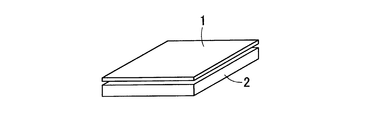
- FIG. 1 is an external view of an X-ray detector according to a first embodiment of the present invention. It is a schematic block diagram of the electrode in the X-ray detector which concerns on the same 1st Embodiment. It is a longitudinal cross-sectional view of the X-ray detector which concerns on the 1st Embodiment. It is a schematic block diagram of the detection circuit of the X-ray detector which concerns on the 1st Embodiment. 2 is a schematic configuration diagram of a conversion unit and a calculation unit of the detection circuit according to the first embodiment. FIG. 3 is a timing chart showing the operation of the detection circuit according to the first embodiment. It is a schematic block diagram of the detection circuit in the X-ray detector which concerns on the 2nd Embodiment of this invention.
- FIG. 1 is an external perspective view of an X-ray detector according to a first embodiment of the present invention.
- the X-ray detector includes a conversion layer 1 that converts incident X-rays into electric charges, and a circuit board 2 on which a detection circuit that counts voltage pulses due to the electric charges is formed.
- the circuit board 2 is a silicon substrate, and a detection circuit is formed using CMOS technology.
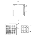
- Electrodes are provided on both the X-ray incident side and the detection circuit side of the conversion layer 1. As shown in FIG. 2A, an electrode 3 common to all pixels is provided on the X-ray incident side of the conversion layer 1.
- each unit pixel area 4 includes a plurality of Sub-pixel electrodes 5 are provided so as to be divided into sub-pixel areas and to correspond to the respective sub-pixel areas.
- the area 4 for one pixel is divided into 16 sub-pixel areas divided into 4 parts vertically and 4 parts horizontally.
- one pixel is 1 mm square, the sub pixel electrode 5 is 200 ⁇ m square, and the space between the sub pixel electrodes 5 is 50 ⁇ m.
- Fig. 3 shows a longitudinal section of the X-ray detector.
- Sub-pixel electrodes 5 provided on the detection circuit (circuit board 2) side of the conversion layer 1 are connected to the detection circuit (circuit board 2) by bumps 6.
- a potential difference is set between the electrode 3 and the sub-pixel electrode 5 provided on both surfaces of the conversion layer 1.
- a plurality of electrons (charges) are generated in the conversion layer 1.
- the charges generated in the conversion layer 1 are moved to the detection circuit (circuit board 2) side by the electric field between the electrode 3 and the sub-pixel electrode 5, and the detection circuit forms a pulse waveform so that X-ray photons are incident. Is detected.
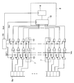
- FIG. 4 shows a schematic configuration of the detection circuit formed on the circuit board 2.
- FIG. 4 shows a detection circuit corresponding to a region for one pixel, and 16 electrodes 6a for forming the bumps 6 of FIG. Further, in the vicinity of each electrode 6a, there is provided a conversion unit 7 for converting the charge generated in the conversion layer 1 into a voltage.
- a calculation unit 8 is provided which receives the outputs of the 16 conversion units 7 and adds the number of X-ray photons of 16 sub-pixels to count the total number of X-ray photons in one frame period.
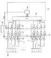
- FIG. 5 shows a schematic configuration of the conversion unit 7 and the calculation unit 8.
- the conversion unit 7 includes a preamplifier 10, a comparator 11, and a flip-flop 12. Electrons (charge signals) generated in the conversion layer 1 are input to the preamplifier 10 via the sub-pixel electrode 5 and the electrode 6a (bump 6) and converted into a voltage value.
- the comparator 11 is supplied with the voltage value output from the preamplifier 10 and the reference voltage Vth, and outputs a signal that becomes a high level while the output voltage value of the preamplifier 10 exceeds the threshold voltage Vth.
- the output of the comparator 11 is given to the flip-flop 12, and at the rising edge of the output value of the comparator 11, the value held and output by the flip-flop 12 becomes High level.
- the calculation unit 8 includes an addition circuit 13 and a counter 14.
- the adder circuit 13 receives the outputs of the 16 conversion units 7 (flip-flops 12), measures the number of output values that are High, and outputs the measured values. In this embodiment, since there are 16 subpixel electrodes 5 and 16 conversion units 7 (flip-flops 12) corresponding thereto, the output of the adder circuit 13 is a 5-bit digital signal.
- the counter 14 receives the output of the adder circuit 13 and counts the output of the adder circuit 13.
- the control circuit 15 outputs reset signals RST1 and RST2 to the integrating capacitor (not shown) and the flip-flop 12 in the preamplifier 10, and resets them at a constant cycle (for example, 100 ns).
- the control circuit 15 outputs the clock signal CLK to the counter 14 at the same fixed period as the reset signals RST1 and RST2 and a predetermined time before outputting the reset signal RST.
- the predetermined time is an extremely short time, and the control circuit 15 outputs the clock signal CLK immediately before the end of a certain period (reset period).
- the adder circuit 13 the number of X-ray photons incident on the sub-pixels whose preamplifier 10 output exceeds the reference voltage Vth is measured by the adder circuit 13 at regular intervals. Further, the output of the adder circuit 13 is counted by the counter 14 at regular intervals.
- the control circuit 15 may be provided in the circuit board 2 or may be an external circuit provided outside the X-ray detector.
- the reference voltage Vth may be output from the control circuit 15.
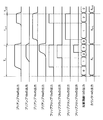
- FIG. 6 shows the outputs of the preamplifiers 10a to 10d and the outputs of the flip-flops 12a to 12d, the output of the adder circuit 13, and the output of the counter 14 of each of the four converters 7.
- the preamplifier is composed of an integrating amplifier, and maintains a voltage value when a voltage value proportional to the amount of charge is shown within the period T.
- the output of the preamplifiers 10a to 10d becomes larger than the reference (threshold) voltage Vth, the output of the comparator 11 at the next stage changes from the low level to the high level, and accordingly, as shown in FIG. 6, the flip-flops 12a to 12d The output changes from Low level to High level.
- the number of flip-flops that are at a high level that is, the number of sub-pixel electrodes on which X-ray photons are incident can be found.
- the clock signal CLK is given to the counter 14 immediately before the end of the period T, and the output value of the adder circuit 13 is counted.
- the reset signal RST1 output from the control circuit 15 discharges the capacitors of the integrating amplifiers of the preamplifiers 10a to 10d, and the outputs of the preamplifiers 10a to 10d become 0V. Further, the flip-flops 12a to 12d are also reset by the reset signal RST2, and the outputs of the flip-flops 12a to 12d become the low level.
- n-th (n is a natural number) period T n in the three flip-flops 12a of, 12b the output of 12d becomes High level, the output value of the adder circuit 13 immediately before the end of the period T n 3 is counted by the counter 14.
- the value of the counter 14 in the period T n + 1 (X n + 1) is intended to 3 were added to the value of the counter 14 in the period T n (X n).
- the outputs of the two flip-flops 12 a and 12 c are at a high level, and the output value 2 of the adder circuit 13 is counted by the counter 14 immediately before the end of the cycle T n + 1 .
- the value of the counter 14 in the period T n + 2 (X n + 2) is intended to 2 was added to the value of the counter 14 in the period T n + 1 (X n + 1).
- the imaging condition is 2000 frames per second (5 ⁇ 10 ⁇ 4 s per frame).
- measurement of about 16384 counts is required for medical X-ray CT, and it can be seen that the number of signals necessary for medical X-ray CT can be obtained by this embodiment.
- the number of voltage pulses generated by the charges generated by the sub-pixel electrodes is added by one pixel and then counted by one counter.
- the circuit scale of the detection circuit can be reduced, the restriction on the number of subpixel divisions is relaxed, and the subpixels are arranged in a two-dimensional array. Thus, the number of divisions can be increased.
- FIG. 7 shows a schematic configuration of a detection circuit in the X-ray detector according to the present embodiment.
- the calculation unit 8 includes a multiplexer 16 and a counter 14. The output of the flip-flop 12 of each converter 7 is input to the multiplexer 16.
- the control circuit 15 outputs the control signal Ctrl to the multiplexer 16 and outputs the clock signal CLK to the counter 14 a predetermined time before the reset cycle ends (outputs the reset signals RST1 and RST2).
- the multiplexer 16 sequentially reads the output of the flip-flop 12 of each conversion unit 7 based on the control signal Ctrl and outputs it to the counter 14.
- the multiplexer 16 reads out the outputs of the flip-flops 12 of all the conversion units 7 and outputs them to the counter 14 before the reset period ends (before the control circuit 15 outputs the reset signals RST1 and RST2).
- the counter 14 counts the output of the multiplexer 16 based on the clock signal CLK.
- the total number of X-ray photons incident on each sub-pixel within a predetermined period is also measured by sequentially reading out the output of the flip-flop 12 corresponding to the sub-pixel every predetermined period and sequentially counting with the counter 14. be able to. Therefore, even if the multiplexer 16 is provided in the calculation unit 8 instead of the adder circuit as in the present embodiment, the same effect as in the first embodiment can be obtained.
- the X-ray detector according to the present embodiment detects that a charge signal is simultaneously generated in two adjacent sub-pixel electrodes, and in that case, by subtracting one count per pixel, X counting by double counting is performed. It suppresses fluctuations in the number of line photons.
- FIG. 8 shows a schematic configuration of a detection circuit in the X-ray detector according to the present embodiment.
- the detection circuit includes a plurality of conversion units 7, a calculation unit 8, a simultaneous incident detection unit 17, and a flip-flop 18 corresponding to each subpixel electrode.
- the conversion unit 7 includes a preamplifier 10, a comparator 11, and a flip-flop 12 as in the first embodiment.
- the simultaneous incident detection unit 17 outputs a detection signal that becomes a high level when the outputs of the comparators 11a and 11b corresponding to the sub-pixel electrodes A and B adjacent to each other become a high level at the same timing.
- the detection signal output from the simultaneous incident detection unit 17 is held by the flip-flop 18 and output to the calculation unit 8.
- the control circuit 15 outputs the reset signal RST1 to the integrating capacitor in the preamplifier 10, the reset signal RST2 to the flip-flops 12 and 18, and the reset signal RST3 to the simultaneous incident detector 17 at a constant cycle, and resets them.
- control circuit 15 outputs the clock signal CLK to the calculation unit 8 at the same constant cycle as the reset signals RST1 to RST3 and a predetermined time before outputting the reset signals RST1 to RST3.
- FIG. 9 shows an example of the circuit configuration of the simultaneous incidence detection unit 17.
- the simultaneous incident detector 17 has an XOR gate 21, a flip-flop 22, and AND gates 23 and 24.
- the XOR gate 21 is supplied with the outputs of the comparators 11a and 11b, and when the outputs of the comparators 11a and 11b are at a high level at different timings, that is, X-ray photons are emitted at different timings to both of the subpixel electrodes A and B adjacent to each other. When incident, a pulse signal is output.
- the flip-flop 22 uses a pulse signal output from the XOR gate as a clock.
- the flip-flop 22 is set so as to be held at a high level by a reset signal RST3 output from the control circuit 15 every fixed period (reset period), and is held at a low level when a clock is input.
- the AND gate 23 is supplied with the outputs of the comparators 11a and 11b, and when the outputs of the comparators 11a and 11b are both at a high level, that is, when X-ray photons are incident on both of the subpixel electrodes A and B adjacent to each other.
- the signal is output.
- the AND gate 24 is supplied with the output of the flip-flop 22 and the output of the AND gate 23.
- the AND gate 24 when both the output of the flip-flop 22 and the output of the AND gate 23 are at a high level, that is, when X-ray photons are incident on both of the sub-pixel electrodes A and B adjacent to each other and the timing is the same. In addition, a high level signal is output.
- the simultaneous incident detectors 17 and flip-flops 18 are provided as many as the boundary regions of adjacent subpixel electrodes.
- the calculation unit 8 includes an addition / subtraction circuit 19 and a counter 14.
- the addition / subtraction circuit 19 adds the output of the conversion unit 7 (flip-flop 12) and subtracts the output of the flip-flop 18. By subtracting the output of the flip-flop 18, it is possible to cancel the double counting.
- the counter 14 counts the measurement value of the addition / subtraction circuit 19 based on the clock signal CLK.
- the number of pulses generated by the charges generated by the sub-pixel electrode is added by one pixel, and the double counting is subtracted and then counted by one counter.
- the circuit scale of the detection circuit can be reduced, the restriction on the number of subpixel divisions is relaxed, and the subpixels are arranged in a two-dimensional array. Thus, the number of divisions can be increased.
- This detection circuit subtracts one photon number even when different X-ray photons are incident on adjacent subpixel electrodes at the same time. However, the probability of this occurrence is very low and the influence is considered to be small. .
- single crystal CdTe is used as the material of the conversion layer 1, but other semiconductor materials may be used.
- a direct conversion type material is used as the material of the conversion layer 1, but an indirect conversion type material may be used.
- a photon counting type X-ray detector can be configured by using an avalanche PD having a quick response as a PD (photodiode) using a scintillator having a short afterglow such as LYSO (Cerium doped Lutetium Orthosilicate).
- a plurality of components (the comparator 11, the flip-flop 12, and the calculation unit 8) after the preamplifier 10 of the detection circuit are provided in parallel, and different reference voltages are applied to the respective comparators 11, thereby obtaining X-ray energy information. Also good.
- comparators 11a to 11d are supplied with the reference voltage Vth1
- comparators 11'a to 11'd are supplied with the reference voltage Vth2 (> Vth1).
- the present invention is not limited to the above-described embodiment as it is, and can be embodied by modifying constituent elements without departing from the scope of the invention in the implementation stage.
- various inventions can be formed by appropriately combining a plurality of components disclosed in the embodiment. For example, some components may be deleted from all the components shown in the embodiment.
- constituent elements over different embodiments may be appropriately combined.
Landscapes
- Engineering & Computer Science (AREA)
- Multimedia (AREA)
- Signal Processing (AREA)
- Physics & Mathematics (AREA)
- Health & Medical Sciences (AREA)
- Life Sciences & Earth Sciences (AREA)
- General Physics & Mathematics (AREA)
- High Energy & Nuclear Physics (AREA)
- Molecular Biology (AREA)
- Spectroscopy & Molecular Physics (AREA)
- Measurement Of Radiation (AREA)
- Solid State Image Pick-Up Elements (AREA)
- Transforming Light Signals Into Electric Signals (AREA)
- Light Receiving Elements (AREA)
Abstract
[課題]検出回路規模を低減し、1画素当たりの分割画素数を大きくできるX線検出器を提供する。 [解決手段]X線を電荷信号に変換する変換層1と、1画素領域をm個(mは2以上の整数)に分割したサブ画素領域4にそれぞれ対応するように設けられた第1~第mのサブ画素電極5と、前記第kのサブ画素電極(kは1≦k≦mを満たす整数)を介して与えられた前記電荷信号を電圧信号に変換して出力する第kの増幅器10と、前記第kの増幅器から出力される前記電圧信号と基準電圧信号Vthとの電圧値を比較し、比較結果を出力する第kの比較器11と、前記第kの比較器から出力される前記比較結果を保持して出力する第kのフリップフロップ12と、前記第1~第mのフリップフロップから出力される前記比較結果を加算してカウントする算出部8と、を備える。
Description
本発明は、X線検出器に関するものである。
近年、X線コンピュータートモグラフィー(X線CT)は、空間分解能や撮影時間の改善により、呼吸器系や消化器系だけでなく、心臓を含めた循環器系や脳の断層診断にも用いられている。
現在のX線CT用X線検出器では、シンチレータによりX線を可視光に変換し、その可視光をフォトダイオードに入射して電荷を生成している。この電荷は検出回路のチャージアンプに送られ、電荷量として検出される。このようなX線の検出方法は電荷積分方式と呼ばれている。この検出方法はアナログ的で、かつノイズが発生しやすい方式である。そのため、所望のS/N比を得るためには、X線照射線量を大きくする必要がある。
電荷積分方式以外のX線検出方法として、検出器に入射したX線のフォトン数を計測するフォトンカウンティング方式が提案されている。この検出方法は、デジタル的な計測方法であり、ノイズを少なくすることが出来るため、X線照射線量を少なくすることが出来る。
しかし、このフォトンカウンティング方式は、X線の入射線量が高い場合、フォトンを時間的に個々に分離することができず、フォトンの数え落としが発生していた。X線フォトン1個を分離してカウントできる最小周期として0.1μsec~2μsec程度は必要となるため、毎秒2000フレーム程度の速度で画像データを検出している医用X線CTにおいては、1フレーム時間内に必要な信号レベルが得られない、という問題があった。
この問題を解決するため、放射線画像の1画素を複数個に分割し、分割画素毎にX線センサでフォトンを検出し、検出したフォトン数をカウントし、分割画素毎のカウント値を加算して1画素分のデータを得る放射線像撮像装置が提案されている(例えば特許文献1参照)。
このように1画素あたりのフォトン数を複数個のX線センサで分割して検出することで、各X線センサに入射するX線線量を低くすることができ、フォトンの数え落としを抑制することが出来る。また、分割画素毎にフォトン数をカウントした場合、分割画素毎のカウント値をそのまま用いることで、空間分解能を向上させたデータが得られる。
このような従来の放射線像撮像装置では、分割画素が1次元的に配列している構成をとっており、画素から検出回路への配線引き出しが容易なので、検出回路も画素を構成するX線変換膜とは別の場所に配置することができる。そのため、検出回路のスペースには制約が少なく、分割画素毎にカウンタを用いてフォトン数をカウントし、各カウンタのカウント値を加算するという構成をとっても問題は無い。
しかし、分割画素が2次元的に配列している場合は、画素からの配線引き出しが困難になり、画素を構成するX線変換膜と回路が構成されている基板とは積層構造になり、両者の間は画素毎にバンプなどで接続されることになる。このような構成では、各画素に必要な検出回路に割けるスペースは各画素の面積と等しくなる。
そのため、従来の放射線像撮像装置のように、分割画素毎にカウンタを用いてフォトン数をカウントし、各カウント値を加算するという回路面積が大きな構成をとることは困難であり、検出回路を形成するスペースを確保するために、1画素当たりの分割数を大きくできないという問題があった。
本発明は検出回路規模を低減し、1画素当たりの分割画素数を大きくできるX線検出器を提供することを目的とする。
本発明の一態様によるX線検出器は、X線を電荷信号に変換する変換層と、前記変換層の第1面に設けられた電極と、前記変換層の前記第1面とは反対の第2面に、2次元マトリクス状に複数設定された画素領域をそれぞれm個(mは2以上の整数)に分割したサブ画素領域にそれぞれ対応するように設けられた第1~第mのサブ画素電極と、前記第kのサブ画素電極(kは1≦k≦mの範囲における連続する整数)を介して前記電荷信号が与えられ、与えられた電荷信号を電圧信号に変換して出力する第kの増幅器と、前記第kの増幅器から出力される前記電圧信号と基準電圧信号とが与えられ、前記電圧信号と前記基準電圧信号との電圧値を比較し、比較結果を出力する第kの比較器と、前記第kの比較器から出力される前記比較結果を保持して出力する第kのフリップフロップと、前記第1~第mのフリップフロップから出力される前記比較結果を加算してカウントする算出部と、を備えるものである。
本発明の一態様によるX線検出器は、X線を電荷信号に変換する変換層と、前記変換層の第1面に設けられた電極と、前記変換層の前記第1面とは反対の第2面に、2次元マトリクス状に複数設定された画素領域をそれぞれm個(mは2以上の整数)に分割した第1~第mのサブ画素領域にそれぞれ対応するように設けられた第1~第mのサブ画素電極と、前記第kのサブ画素電極(kは1≦k≦mの範囲における連続する整数)を介して前記電荷信号が与えられ、与えられた電荷信号を電圧信号に変換して出力する第kの増幅器と、前記第kの増幅器から出力される前記電圧信号と基準電圧信号とが与えられ、前記電圧信号と前記基準電圧信号との電圧値を比較し、比較結果を出力する第kの比較器と、前記第kの比較器から出力される前記比較結果を保持して出力する第kのフリップフロップと、それぞれ、互いに隣接する2つの前記サブ画素領域に対応する2つの前記比較器から出力される前記比較結果が与えられ、前記2つの比較器から出力される前記比較結果が同じタイミングでハイレベルになった場合に検出信号を出力する複数の同時入射検出部と、対応する前記同時入射検出部から出力される前記検出信号を保持して出力する複数の第m+1のフリップフロップと、前記第1~第mのフリップフロップから出力される前記比較結果を加算し、前記複数の第m+1のフリップフロップから出力される前記検出信号を減算し、計算結果を出力する加減算回路と、前記加減算回路から出力される前記計算結果をカウントするカウンタと、を備えるものである。
本発明の一態様によるX線検出器は、X線を電荷信号に変換する変換層と、前記変換層の第1面に設けられた電極と、前記変換層の前記第1面とは反対の第2面に、2次元マトリクス状に複数設定された画素領域をそれぞれm個(mは2以上の整数)に分割したサブ画素領域にそれぞれ対応するように設けられた第1~第mのサブ画素電極と、前記第kのサブ画素電極(kは1≦k≦mの範囲における連続する整数)を介して前記電荷信号が与えられ、与えられた電荷信号を電圧信号に変換して出力する第kの増幅器と、前記第kの増幅器から出力される前記電圧信号及び第jの基準電圧信号(jは1≦j≦nの範囲における連続する整数であり、nは2以上の整数)が与えられ、前記電圧信号と前記第jの基準電圧信号との電圧値を比較し、比較結果を出力する第kの比較器を含む第jの比較器群と、前記第jの比較器群に含まれる前記第kの比較器から出力される前記比較結果を保持して出力する第kのフリップフロップを含む第jのフリップフロップ群と、前記第jのフリップフロップ群に含まれる前記第1~第mのフリップフロップから出力される前記比較結果を加算してカウントする第jの算出部と、を備えるものである。
本発明によれば、検出回路規模を低減し、1画素当たりの分割画素数を大きくできる。
以下、本発明の実施の形態によるX線検出器を図面に基づいて説明する。
(第1の実施形態)図1は本発明の第1の実施形態に係るX線検出器の外観斜視図である。X線検出器は、入射したX線を電荷に変換する変換層1と、その電荷による電圧パルスをカウントする検出回路が形成されている回路基板2と、を備える。
本実施形態では、変換層1として単結晶CdTeを用いている。また、回路基板2はシリコン基板であり、CMOS技術を用いて検出回路が形成されている。
変換層1のX線入射側と検出回路側の両面にはそれぞれ電極が設けられている。図2(a)に示すように、変換層1のX線入射側には全画素に共通した電極3が設けられている。
また、図2(b)に示すように、変換層1の検出回路側は、1画素分の領域(単位画素領域)4が2次元マトリクス状に複数設定され、各単位画素領域4は複数のサブ画素領域に分割され、各サブ画素領域に対応するようにサブ画素電極5が設けられている。本実施形態では、1画素分の領域4を縦4分割、横4分割の16個のサブ画素領域に分割している。
例えば、1画素は1mm角、サブ画素電極5は200μm角、サブ画素電極5間のスペースは50μmとなる。
図3にX線検出器の縦断面を示す。変換層1の検出回路(回路基板2)側に設けられたサブ画素電極5はバンプ6により検出回路(回路基板2)と接続されている。変換層1の両面に設けられた電極3とサブ画素電極5との間には電位差が設定されている。変換層1にX線が入射すると、変換層1内で複数の電子(電荷)が発生する。変換層1内で発生した電荷は、電極3、サブ画素電極5間の電界により検出回路(回路基板2)側へ移動し、検出回路でパルス波形を形成することで、X線のフォトンが入射したことが検知される。
図4に回路基板2に形成された検出回路の概略構成を示す。図4は1画素分の領域に対応する検出回路を示しており、図3のバンプ6を形成する電極6aが縦4個、横4個の計16個設けられている。また、各々の電極6aの近傍には、変換層1で生じた電荷を電圧に変換する変換部7が設けられている。
また、16個の変換部7の出力が与えられ、16個のサブ画素のX線フォトン数を加算し、1フレーム期間内のX線フォトンの総数をカウントする算出部8が設けられている。
図5に変換部7及び算出部8の概略構成を示す。変換部7はプリアンプ10、コンパレータ11、及びフリップフロップ12を有する。変換層1内で発生した電子(電荷信号)はサブ画素電極5、電極6a(バンプ6)を介してプリアンプ10に入力し、電圧値に変換される。
コンパレータ11は、プリアンプ10から出力される電圧値と基準電圧Vthとが与えられ、プリアンプ10の出力電圧値が閾値電圧Vthを超えている間にHighレベルとなる信号を出力する。
コンパレータ11の出力はフリップフロップ12に与えられ、コンパレータ11の出力値の立ち上がりで、フリップフロップ12の保持及び出力する値がHighレベルになる。
算出部8は加算回路13及びカウンタ14を有する。加算回路13は16個の変換部7(フリップフロップ12)の出力が与えられ、出力値がHighになっている個数を計測し、計測値を出力する。本実施形態ではサブ画素電極5が16個あり、それに対応する変換部7(フリップフロップ12)も16個あるため、加算回路13の出力は5ビットのデジタル信号となる。
カウンタ14は、加算回路13の出力が与えられ、加算回路13の出力をカウントする。
制御回路15は、プリアンプ10内の積分コンデンサ(図示せず)及びフリップフロップ12にリセット信号RST1、RST2を出力し、一定周期(例えば100ns)でリセットする。また、制御回路15は、リセット信号RST1、RST2と同じ一定周期で、かつリセット信号RSTを出力する所定時間前に、クロック信号CLKをカウンタ14へ出力する。なお、この所定時間は極めて短い時間とし、制御回路15はクロック信号CLKを一定周期(リセット周期)の終了直前に出力する。
これにより、サブ画素に入射するX線フォトンのうち、プリアンプ10出力が基準電圧Vthを超えるものの個数が、一定周期ごとに加算回路13で計測される。また、加算回路13の出力が一定周期ごとにカウンタ14でカウントされる。
制御回路15は回路基板2内に設けてもよく、またX線検出器外に設けた外部回路としてもよい。基準電圧Vthは制御回路15から出力するようにしてもよい。
検出回路の動作を図6に示すタイミングチャートを用いて説明する。ここでは、説明の便宜上、変換部7の個数を4つとする。図6は4つの変換部7の各々のプリアンプ10a~10dの出力及びフリップフロップ12a~12dの出力と、加算回路13の出力と、カウンタ14の出力と、を示す。
X線が変換層1に入射し、発生した電荷信号がサブ画素電極5を介してプリアンプに入力されると、図6に示すように、プリアンプ10a~10dの出力は電荷信号の電荷量に比例した電圧値を示す。プリアンプは積分アンプで構成されており、周期T内で電荷量に比例した電圧値を示すと、その電圧値を維持する。
プリアンプ10a~10dの出力が、基準(閾値)電圧Vthより大きくなると、次段のコンパレータ11出力がLowレベルからHighレベルになり、これに伴い、図6に示すように、フリップフロップ12a~12dの出力がLowレベルからHighレベルに変わる。
周期Tの終了時点での加算回路13の出力値から、Highレベルになっているフリップフロップの数、すなわちX線フォトンが入射したサブ画素電極の数がわかる。周期Tの終了直前にカウンタ14にクロック信号CLKが与えられ、加算回路13の出力値がカウントされる。
周期Tが終了すると、制御回路15から出力されるリセット信号RST1により、プリアンプ10a~10dの積分アンプのコンデンサが放電され、プリアンプ10a~10dの出力は0Vになる。また、リセット信号RST2によりフリップフロップ12a~12dもリセットされ、フリップフロップ12a~12dの出力はLowレベルになる。
例えば、図6に示すように、n番目(nは自然数)の周期Tnでは3つのフリップフロップ12a、12b、12dの出力がHighレベルとなり、周期Tnの終了直前に加算回路13の出力値3がカウンタ14でカウントされる。これにより、周期Tn+1でのカウンタ14の値(Xn+1)は周期Tnでのカウンタ14の値(Xn)に3を加えたものとなる。
周期Tnが終了すると、プリアンプ10a~10dの出力は0Vになり、フリップフロップ12a~12dの出力はLowレベルになる。
周期Tn+1では2つのフリップフロップ12a、12cの出力がHighレベルとなり、周期Tn+1の終了直前に加算回路13の出力値2がカウンタ14でカウントされる。これにより、周期Tn+2でのカウンタ14の値(Xn+2)は周期Tn+1でのカウンタ14の値(Xn+1)に2を加えたものとなる。
周期Tn+1が終了すると、プリアンプ10a~10dの出力は0Vになり、フリップフロップ12a~12dの出力はLowレベルになる。
本実施形態のように16個のサブ画素電極5、変換部7でX線を検出する場合、リセット周期Tを100nsとすると、毎秒2000フレーム(1フレーム当たり5×10⁻⁴s)の撮影条件で、フォトン数として80000カウントまで計測が可能となる。例えば、一般に医用X線CTでは16384カウント程度の計測が求められており、本実施形態により医用X線CTで必要な信号数が得られることがわかる。
本実施形態では、サブ画素電極で生成された電荷により発生する電圧パルスの数を1画素分加算してから1つのカウンタでカウントしている。つまり複数のサブ画素に分割される1画素あたりにカウンタの数を1つにできるので、検出回路の回路規模を削減でき、サブ画素の分割数の制約が緩和され、サブ画素を2次元配列等にして分割数を大きくすることができる。
(第2の実施形態)本発明の第2の実施形態に係るX線検出器について説明する。検出回路の算出部8以外の変換層1、電極3、サブ画素電極5、変換部7は上記第1の実施形態(図1~図4参照)と同様であるため、説明を省略する。
図7に本実施形態に係るX線検出器における検出回路の概略構成を示す。算出部8はマルチプレクサ16及びカウンタ14を有する。各変換部7のフリップフロップ12の出力はマルチプレクサ16に入力される。
制御回路15は、リセット周期が終了する(リセット信号RST1、RST2を出力する)所定時間前に、マルチプレクサ16へ制御信号Ctrlを出力し、カウンタ14へクロック信号CLKを出力する。
マルチプレクサ16は、制御信号Ctrlに基づいて、各変換部7のフリップフロップ12の出力を順次読み出してカウンタ14へ出力する。マルチプレクサ16はリセット周期が終了する前(制御回路15がリセット信号RST1、RST2を出力する前)に、すべての変換部7のフリップフロップ12の出力を読み出してカウンタ14へ出力する。
カウンタ14はクロック信号CLKに基づいて、マルチプレクサ16の出力をカウントする。
このように、一定周期毎にサブ画素に対応するフリップフロップ12の出力を順次読み出して、カウンタ14で順次カウントすることでも、一定周期内に各サブ画素に入射したX線フォトンの総数を計測することができる。従って、本実施形態のように算出部8に加算回路でなくマルチプレクサ16を設けるようにしても、上記第1の実施形態と同様の効果を得ることができる。
(第3の実施形態)本発明の第3の実施形態に係るX線検出器について説明する。検出回路以外の変換層1、電極3、サブ画素電極5、変換部7は上記第1の実施形態(図1~図4参照)と同様であるため、説明を省略する。
互いに隣接したサブ画素電極間にX線フォトンが入射すると、両方のサブ画素電極へ電荷信号が流れ込み、フォトン数の二重数えが発生する。1画素の分割数(サブ画素数)を大きくしていくと、この現象が生じる隣接サブ画素電極の境界領域が増えて、二重数えが頻発するおそれがある。
本実施形態によるX線検出器は、隣接した2つのサブ画素電極で同時に電荷信号が発生することを検出し、その場合は1画素あたりのカウント数を1つ減じることで、二重数えによるX線フォトンのカウント数の変動を抑制するものである。
図8に本実施形態に係るX線検出器における検出回路の概略構成を示す。検出回路は各サブ画素電極に対応する複数の変換部7、算出部8、同時入射検出部17、及びフリップフロップ18を有する。変換部7は上記第1の実施形態と同様にプリアンプ10、コンパレータ11、及びフリップフロップ12を有する。
同時入射検出部17は、互いに隣接するサブ画素電極A、Bに対応するコンパレータ11a、11bの出力が同じタイミングでHighレベルになった場合にHighレベルとなる検出信号を出力する。
同時入射検出部17から出力される検出信号はフリップフロップ18で保持され、算出部8へ出力される。
制御回路15は一定周期で、プリアンプ10内の積分コンデンサへリセット信号RST1を、フリップフロップ12及び18へリセット信号RST2を、同時入射検出部17へリセット信号RST3を出力し、これらをリセットする。
また、制御回路15は、リセット信号RST1~3と同じ一定周期で、かつリセット信号RST1~3を出力する所定時間前に、クロック信号CLKを算出部8へ出力する。
図9に同時入射検出部17の回路構成の一例を示す。同時入射検出部17はXORゲート21、フリップフロップ22、ANDゲート23、24を有する。
XORゲート21はコンパレータ11a、11bの出力が与えられ、コンパレータ11a、11bの出力が異なるタイミングでHighレベルになる時、すなわち互いに隣接するサブ画素電極A、Bの両方に異なるタイミングでX線フォトンが入射した時に、パルス信号を出力する。
フリップフロップ22はXORゲートから出力されるパルス信号をクロックとする。このフリップフロップ22は一定周期(リセット周期)毎に制御回路15から出力されるリセット信号RST3によりHighレベルを保持するようにセットされ、クロックが入力するとLowレベルを保持する。
ANDゲート23はコンパレータ11a、11bの出力が与えられ、コンパレータ11a、11bの出力が共にHighレベルの時、すなわち互いに隣接するサブ画素電極A、Bの両方にX線フォトンが入射した時に、Highレベルの信号を出力する。
ANDゲート24はフリップフロップ22の出力とANDゲート23の出力が与えられる。ANDゲート24は、フリップフロップ22の出力とANDゲート23の出力が共にHighレベルのとき、すなわち互いに隣接するサブ画素電極A、Bの両方にX線フォトンが入射し、そのタイミングが同時であるときに、Highレベルの信号を出力する。
この同時入射検出部17及びフリップフロップ18は隣接サブ画素電極の境界領域の数だけ設けられる。
算出部8は加減算回路19及びカウンタ14を有する。加減算回路19は変換部7(フリップフロップ12)の出力を加算し、フリップフロップ18の出力を減算する。フリップフロップ18の出力を減算することで、二重数えした分を相殺することができる。
カウンタ14はクロック信号CLKに基づいて、加減算回路19の計測値をカウントする。
このように、本実施形態では、サブ画素電極で生成された電荷により発生するパルスの数を1画素分加算し、二重数えの分を減算してから1つのカウンタでカウントしている。つまり複数のサブ画素に分割される1画素あたりにカウンタの数を1つにできるので、検出回路の回路規模を削減でき、サブ画素の分割数の制約が緩和され、サブ画素を2次元配列等にして分割数を大きくすることができる。
また、互いに隣接するサブ画素電極に対応する変換部7のコンパレータ出力を用いて、X線フォトンが同時に入射したか否かを検出でき、フォトン数の2重数えを防止できる。
この検出回路は、隣接したサブ画素電極に異なるX線フォトンが同時に入射した時もフォトン数を1つ減算してしまうが、このようなことが起こる確率は非常に低く、影響は小さいと考えられる。
上記実施形態では変換層1の材料として単結晶CdTeを用いていたが、その他の半導体材料を用いてもよい。
また、上記実施形態では変換層1の材料として、直接変換方式の材料を用いているが、間接変換方式の材料でもよい。例えば、シンチレータとしてLYSO(Cerium doped Lutetium Orthosilicate)のような残光が短いものを用い、PD(フォトダイオード)として応答の速いアバランシェPDを用いることで、フォトンカウンティング方式のX線検出器を構成できる。
検出回路のプリアンプ10以降の構成要素(コンパレータ11、フリップフロップ12、算出部8)を並列に複数設け、それぞれのコンパレータ11に異なる基準電圧を与えることで、X線のエネルギー情報を得るようにしてもよい。
例えば図10に示すように、プリアンプ10a~10dの後段に、コンパレータ11a~11d、フリップフロップ12a~12d、加算回路13、及びカウンタ14と、コンパレータ11’a~11’d、フリップフロップ12’a~12’d、加算回路13’、及びカウンタ14’とを並列に設ける。コンパレータ11a~11dには基準電圧Vth1を与え、コンパレータ11’a~11’dには基準電圧Vth2(>Vth1)を与える。カウンタ14、14’のカウント値を用いることで、異なるエネルギーの弁別画像を得ることができる。
なお、本発明は上記実施形態そのままに限定されるものではなく、実施段階ではその要旨を逸脱しない範囲で構成要素を変形して具体化できる。また、上記実施形態に開示されている複数の構成要素の適宜な組み合わせにより、種々の発明を形成できる。例えば、実施形態に示される全構成要素から幾つかの構成要素を削除してもよい。さらに、異なる実施形態にわたる構成要素を適宜組み合わせてもよい。
1 変換層
2 回路基板
3 電極
4 1画素領域
5 サブ画素電極
6 バンプ
7 変換部
8 算出部
10 プリアンプ
11 コンパレータ
12、18 フリップフロップ
13 加算回路
14 カウンタ
15 制御回路
16 マルチプレクサ
17 同時入射検出部
19 加減算回路
2 回路基板
3 電極
4 1画素領域
5 サブ画素電極
6 バンプ
7 変換部
8 算出部
10 プリアンプ
11 コンパレータ
12、18 フリップフロップ
13 加算回路
14 カウンタ
15 制御回路
16 マルチプレクサ
17 同時入射検出部
19 加減算回路
Claims (15)
- X線を電荷信号に変換する変換層と、
前記変換層の第1面に設けられた電極と、
前記変換層の前記第1面とは反対の第2面に、2次元マトリクス状に複数設定された画素領域をそれぞれm個(mは2以上の整数)に分割したサブ画素領域にそれぞれ対応するように設けられた第1~第mのサブ画素電極と、
前記第kのサブ画素電極(kは1≦k≦mの範囲における連続する整数)を介して前記電荷信号が与えられ、与えられた電荷信号を電圧信号に変換して出力する第kの増幅器と、
前記第kの増幅器から出力される前記電圧信号と基準電圧信号とが与えられ、前記電圧信号と前記基準電圧信号との電圧値を比較し、比較結果を出力する第kの比較器と、
前記第kの比較器から出力される前記比較結果を保持して出力する第kのフリップフロップと、
前記第1~第mのフリップフロップから出力される前記比較結果を加算してカウントする算出部と、
を備えるX線検出器。 - 前記算出部は、
前記第1~第mのフリップフロップから出力される前記比較結果を加算し、加算結果を出力する加算回路と、
前記加算回路から出力される前記加算結果をカウントするカウンタと、
を有することを特徴とする請求項1に記載のX線検出器。 - 所定周期毎に、前記第1~第mの増幅器及び前記第1~第mのフリップフロップへリセット信号を出力し、前記リセット信号を出力する所定時間前に前記カウンタへクロック信号を出力する制御回路をさらに備え、
前記第1~第mの増幅器及び前記第1~第mのフリップフロップは前記リセット信号に基づいてリセットされ、前記カウンタは前記クロック信号に基づいて前記加算結果をカウントすることを特徴とする請求項2に記載のX線検出器。 - 前記算出部は、
前記第1~第mのフリップフロップから出力される前記比較結果が与えられ、前記比較結果を順次選択して出力するマルチプレクサと、
前記マルチプレクサから出力される前記比較結果を順次カウントするカウンタと、
を有することを特徴とする請求項1に記載のX線検出器。 - 所定周期毎に、前記第1~第mの増幅器及び前記第1~第mのフリップフロップへリセット信号を出力し、前記リセット信号を出力する所定時間前に前記マルチプレクサへ制御信号を出力すると共に前記カウンタへクロック信号を出力する制御回路をさらに備え、
前記第1~第mの増幅器及び前記第1~第mのフリップフロップは前記リセット信号に基づいてリセットされ、前記マルチプレクサは前記制御信号に基づいて前記比較結果の選択及び出力を開始し、前記カウンタは前記クロック信号に基づいて前記比較結果をカウントすることを特徴とする請求項4に記載のX線検出器。 - X線を電荷信号に変換する変換層と、
前記変換層の第1面に設けられた電極と、
前記変換層の前記第1面とは反対の第2面に、2次元マトリクス状に複数設定された画素領域をそれぞれm個(mは2以上の整数)に分割した第1~第mのサブ画素領域にそれぞれ対応するように設けられた第1~第mのサブ画素電極と、
前記第kのサブ画素電極(kは1≦k≦mの範囲における連続する整数)を介して前記電荷信号が与えられ、与えられた電荷信号を電圧信号に変換して出力する第kの増幅器と、
前記第kの増幅器から出力される前記電圧信号と基準電圧信号とが与えられ、前記電圧信号と前記基準電圧信号との電圧値を比較し、比較結果を出力する第kの比較器と、
前記第kの比較器から出力される前記比較結果を保持して出力する第kのフリップフロップと、
それぞれ、互いに隣接する2つの前記サブ画素領域に対応する2つの前記比較器から出力される前記比較結果が与えられ、前記2つの比較器から出力される前記比較結果が同じタイミングでハイレベルになった場合に検出信号を出力する複数の同時入射検出部と、
対応する前記同時入射検出部から出力される前記検出信号を保持して出力する複数の第m+1のフリップフロップと、
前記第1~第mのフリップフロップから出力される前記比較結果を加算し、前記複数の第m+1のフリップフロップから出力される前記検出信号を減算し、計算結果を出力する加減算回路と、
前記加減算回路から出力される前記計算結果をカウントするカウンタと、
を備えるX線検出器。 - 所定周期毎に、前記第1~第mの増幅器、前記第1~第mのフリップフロップ、前記複数の第m+1のフリップフロップ、及び前記同時入射検出部へリセット信号を出力し、前記リセット信号を出力する所定時間前に前記カウンタへクロック信号を出力する制御回路をさらに備え、
前記第1~第mの増幅器、前記第1~第mのフリップフロップ、前記複数の第m+1のフリップフロップ、及び前記同時入射検出部は前記リセット信号に基づいてリセットされ、前記カウンタは前記クロック信号に基づいて前記計算結果をカウントすることを特徴とする請求項6に記載のX線検出器。 - 前記複数の同時入射検出部はそれぞれ、
前記互いに隣接する2つの前記サブ画素領域に対応する2つの前記比較器から出力される前記比較結果が与えられるXORゲートと、
前記XORゲートの出力をクロック入力とし、クロックが与えられるとロウレベルを保持して出力する第m+2のフリップフロップと、
前記互いに隣接する2つの前記サブ画素領域に対応する2つの前記比較器から出力される前記比較結果が与えられる第1のANDゲートと、
前記第m+2のフリップフロップの出力及び前記第1のANDゲートの出力が与えられ、前記検出信号を出力する第2のANDゲートと、
を有することを特徴とする請求項6に記載のX線検出器。 - 所定周期毎に、前記第1~第mの増幅器、前記第1~第mのフリップフロップ、前記複数の第m+1のフリップフロップ、及び前記第m+2のフリップフロップへリセット信号を出力し、前記リセット信号を出力する所定時間前に前記カウンタへクロック信号を出力する制御回路をさらに備え、
前記第1~第mの増幅器、前記第1~第mのフリップフロップ、及び前記複数の第m+1のフリップフロップは前記リセット信号に基づいてリセットされ、前記第m+2のフリップフロップは前記リセット信号に基づいてハイレベルを保持して出力し、前記カウンタは前記クロック信号に基づいて前記計算結果をカウントすることを特徴とする請求項8に記載のX線検出器。 - X線を電荷信号に変換する変換層と、
前記変換層の第1面に設けられた電極と、
前記変換層の前記第1面とは反対の第2面に、2次元マトリクス状に複数設定された画素領域をそれぞれm個(mは2以上の整数)に分割したサブ画素領域にそれぞれ対応するように設けられた第1~第mのサブ画素電極と、
前記第kのサブ画素電極(kは1≦k≦mの範囲における連続する整数)を介して前記電荷信号が与えられ、与えられた電荷信号を電圧信号に変換して出力する第kの増幅器と、
前記第kの増幅器から出力される前記電圧信号及び第jの基準電圧信号(jは1≦j≦nの範囲における連続する整数であり、nは2以上の整数)が与えられ、前記電圧信号と前記第jの基準電圧信号との電圧値を比較し、比較結果を出力する第kの比較器を含む第jの比較器群と、
前記第jの比較器群に含まれる前記第kの比較器から出力される前記比較結果を保持して出力する第kのフリップフロップを含む第jのフリップフロップ群と、
前記第jのフリップフロップ群に含まれる前記第1~第mのフリップフロップから出力される前記比較結果を加算してカウントする第jの算出部と、
を備えるX線検出器。 - 前記第1~第nの算出部はそれぞれ、
前記第1~第mのフリップフロップから出力される前記比較結果を加算し、加算結果を出力する加算回路と、
前記加算回路から出力される前記加算結果をカウントするカウンタと、
を有することを特徴とする請求項10に記載のX線検出器。 - 所定周期毎に、前記第1~第mの増幅器及び前記第1~第nのフリップフロップ群に含まれる前記第1~第mのフリップフロップへリセット信号を出力し、前記リセット信号を出力する所定時間前に前記第1~第nの算出部に含まれる前記カウンタへクロック信号を出力する制御回路をさらに備え、
前記第1~第mの増幅器及び前記第1~第nのフリップフロップ群に含まれる前記第1~第mのフリップフロップは前記リセット信号に基づいてリセットされ、前記カウンタは前記クロック信号に基づいて前記加算結果をカウントすることを特徴とする請求項11に記載のX線検出器。 - 前記第1~第nの算出部はそれぞれ、
前記第1~第mのフリップフロップから出力される前記比較結果が与えられ、前記比較結果を順次選択して出力するマルチプレクサと、
前記マルチプレクサから出力される前記比較結果を順次カウントするカウンタと、
を有することを特徴とする請求項10に記載のX線検出器。 - 所定周期毎に、前記第1~第mの増幅器及び前記第1~第nのフリップフロップ群に含まれる前記第1~第mのフリップフロップへリセット信号を出力し、前記リセット信号を出力する所定時間前に前記第1~第nの算出部に含まれる前記マルチプレクサへ制御信号を出力すると共に前記カウンタへクロック信号を出力する制御回路をさらに備え、
前記第1~第mの増幅器及び前記第1~第nのフリップフロップ群に含まれる前記第1~第mのフリップフロップは前記リセット信号に基づいてリセットされ、前記マルチプレクサは前記制御信号に基づいて前記比較結果の選択を開始し、前記カウンタは前記クロック信号に基づいて前記比較結果をカウントすることを特徴とする請求項13に記載のX線検出器。 - 前記第1~第nの基準電圧信号はそれぞれ電圧値が異なることを特徴とする請求項10に記載のX線検出器。
Priority Applications (1)
| Application Number | Priority Date | Filing Date | Title |
|---|---|---|---|
| US13/052,681 US20110168909A1 (en) | 2008-09-24 | 2011-03-21 | X-ray detector |
Applications Claiming Priority (2)
| Application Number | Priority Date | Filing Date | Title |
|---|---|---|---|
| JP2008-243816 | 2008-09-24 | ||
| JP2008243816A JP2010078338A (ja) | 2008-09-24 | 2008-09-24 | X線検出器 |
Related Child Applications (1)
| Application Number | Title | Priority Date | Filing Date |
|---|---|---|---|
| US13/052,681 Continuation US20110168909A1 (en) | 2008-09-24 | 2011-03-21 | X-ray detector |
Publications (1)
| Publication Number | Publication Date |
|---|---|
| WO2010035671A1 true WO2010035671A1 (ja) | 2010-04-01 |
Family
ID=42059672
Family Applications (1)
| Application Number | Title | Priority Date | Filing Date |
|---|---|---|---|
| PCT/JP2009/066170 Ceased WO2010035671A1 (ja) | 2008-09-24 | 2009-09-16 | X線検出器 |
Country Status (3)
| Country | Link |
|---|---|
| US (1) | US20110168909A1 (ja) |
| JP (1) | JP2010078338A (ja) |
| WO (1) | WO2010035671A1 (ja) |
Cited By (2)
| Publication number | Priority date | Publication date | Assignee | Title |
|---|---|---|---|---|
| JP2012187143A (ja) * | 2011-03-08 | 2012-10-04 | Toshiba Corp | X線コンピュータ断層撮影装置 |
| US10338012B2 (en) | 2016-03-09 | 2019-07-02 | Toshiba Medical Systems Corporation | Photon counting detector and X-ray computed tomography (CT) apparatus |
Families Citing this family (25)
| Publication number | Priority date | Publication date | Assignee | Title |
|---|---|---|---|---|
| DE102009055807B4 (de) * | 2009-11-26 | 2016-11-24 | Siemens Healthcare Gmbh | Schaltungsanordnung zur Zählung von Röntgenquanten einer Röntgenstrahlung mittels quantenzählender Detektoren sowie anwendungsspezifische integrierte Schaltung und Strahler-Detektor-System |
| BR112013009965A8 (pt) * | 2010-10-27 | 2016-09-13 | Koninklijke Philips Electronics Nv | "sistema e método" |
| JP2014535039A (ja) * | 2011-09-30 | 2014-12-25 | アナロジック コーポレイション | 光子数の補正方法および装置{photoncountcorrection} |
| JP6159133B2 (ja) * | 2013-04-23 | 2017-07-05 | 株式会社堀場製作所 | 放射線検出器、放射線検出方法及びコンピュータプログラム |
| KR101635980B1 (ko) * | 2013-12-30 | 2016-07-05 | 삼성전자주식회사 | 방사선 디텍터 및 그에 따른 컴퓨터 단층 촬영 장치 |
| WO2015105314A1 (en) | 2014-01-07 | 2015-07-16 | Samsung Electronics Co., Ltd. | Radiation detector, tomography imaging apparatus thereof, and radiation detecting apparatus thereof |
| WO2015129069A1 (ja) * | 2014-02-27 | 2015-09-03 | 富士電機株式会社 | 放射線検出装置、放射線量計測処理方法、及び放射線量計測処理プログラム |
| DE102014204042A1 (de) * | 2014-03-05 | 2015-09-10 | Siemens Aktiengesellschaft | Verfahren zur Ansteuerung eines Röntgendetektors und zugehörige Steuereinheit |
| KR20160048535A (ko) * | 2014-10-24 | 2016-05-04 | 삼성전자주식회사 | 엑스선 디텍터와 그 제조방법과 엑스선 디텍터를 포함하는 시스템과 그 동작방법 |
| KR101646651B1 (ko) * | 2014-10-30 | 2016-08-08 | 서강대학교산학협력단 | 다중 문턱전압을 이용한 의료 영상기기의 신호처리 시스템 및 방법 |
| CN107005664A (zh) * | 2014-11-20 | 2017-08-01 | 株式会社岛津制作所 | 光检测器 |
| US10732906B2 (en) * | 2015-02-26 | 2020-08-04 | Seagate Technology Llc | Multi-device storage with consolidated channel and control circuitry |
| US10456099B2 (en) * | 2015-08-24 | 2019-10-29 | Hitachi, Ltd. | Radiation detecting device and medical imaging device |
| US9851460B1 (en) * | 2016-09-07 | 2017-12-26 | Toshiba Medical Systmes Corporation | Apparatus and method for a high-flux photon-counting spectral application-specific integrated circuit (ASIC) having a charge summing mode |
| WO2018133087A1 (en) | 2017-01-23 | 2018-07-26 | Shenzhen Xpectvision Technology Co., Ltd. | X-ray detectors capable of identifying and managing charge sharing |
| KR101905690B1 (ko) * | 2017-02-08 | 2018-11-21 | 서강대학교산학협력단 | 지연소자를 이용한 멀티플렉싱 신호처리 장치 |
| JP6800047B2 (ja) * | 2017-02-27 | 2020-12-16 | 株式会社日立製作所 | X線撮像装置 |
| US20180329064A1 (en) * | 2017-05-09 | 2018-11-15 | Stmicroelectronics (Grenoble 2) Sas | Method and apparatus for mapping column illumination to column detection in a time of flight (tof) system |
| JP7337056B2 (ja) * | 2018-07-03 | 2023-09-01 | ソニーセミコンダクタソリューションズ株式会社 | 固体撮像装置 |
| JP2020010150A (ja) * | 2018-07-06 | 2020-01-16 | ソニーセミコンダクタソリューションズ株式会社 | 撮像装置および撮像システム |
| JP7337517B2 (ja) | 2019-03-14 | 2023-09-04 | 株式会社東芝 | 光検出器及び距離測定装置 |
| US12360258B2 (en) | 2020-03-30 | 2025-07-15 | National University Corporation Shizuoka University | Radiation image sensor |
| JP7733921B2 (ja) | 2020-05-29 | 2025-09-04 | ボクセルセンサー エスアールエル | ピクセルセンサーシステム |
| JP7612251B2 (ja) * | 2020-12-23 | 2025-01-14 | ボクセルセンサーズ エスアールエル | 近隣ゲートによってスイッチする画素センサ |
| BE1029563B1 (nl) * | 2021-07-05 | 2023-02-06 | Voxelsensors Srl | Pixel array met dynamische laterale en temporele resolutie |
Citations (8)
| Publication number | Priority date | Publication date | Assignee | Title |
|---|---|---|---|---|
| JPH02257085A (ja) * | 1989-03-30 | 1990-10-17 | Shimadzu Corp | 放射線測定装置 |
| JPH05209967A (ja) * | 1992-01-31 | 1993-08-20 | Shimadzu Corp | 放射線像撮像装置 |
| JPH095445A (ja) * | 1995-06-23 | 1997-01-10 | Shimadzu Corp | 放射線像撮像装置 |
| JP2000131440A (ja) * | 1998-10-20 | 2000-05-12 | Toshiba Corp | 放射線検出処理システム |
| JP2004000734A (ja) * | 1992-03-24 | 2004-01-08 | Varian Medical Systems Inc | 改良されたx線ct装置の使用方法 |
| JP2006519368A (ja) * | 2003-02-14 | 2006-08-24 | シーメンス アクチエンゲゼルシヤフト | X線検出器 |
| JP2006234727A (ja) * | 2005-02-28 | 2006-09-07 | Toshiba Corp | 放射線分布撮影装置および放射線分布撮影方法 |
| WO2007015777A1 (en) * | 2005-07-26 | 2007-02-08 | Ge Medical Systems Isreal, Ltd. | Method and apparatus for acquiring radiation data |
Family Cites Families (3)
| Publication number | Priority date | Publication date | Assignee | Title |
|---|---|---|---|---|
| DE69525477T2 (de) * | 1995-07-31 | 2002-11-07 | Ifire Technology Inc., Fort Saskatchewan | Flacher detektor für strahlungsabbildung mit reduzierten gespeicherten ladungen |
| GB2318411B (en) * | 1996-10-15 | 1999-03-10 | Simage Oy | Imaging device for imaging radiation |
| JP2004325183A (ja) * | 2003-04-23 | 2004-11-18 | M & C:Kk | 放射線検出方法、放射線検出器、及び、この検出器を搭載した放射線撮像システム |
-
2008
- 2008-09-24 JP JP2008243816A patent/JP2010078338A/ja active Pending
-
2009
- 2009-09-16 WO PCT/JP2009/066170 patent/WO2010035671A1/ja not_active Ceased
-
2011
- 2011-03-21 US US13/052,681 patent/US20110168909A1/en not_active Abandoned
Patent Citations (8)
| Publication number | Priority date | Publication date | Assignee | Title |
|---|---|---|---|---|
| JPH02257085A (ja) * | 1989-03-30 | 1990-10-17 | Shimadzu Corp | 放射線測定装置 |
| JPH05209967A (ja) * | 1992-01-31 | 1993-08-20 | Shimadzu Corp | 放射線像撮像装置 |
| JP2004000734A (ja) * | 1992-03-24 | 2004-01-08 | Varian Medical Systems Inc | 改良されたx線ct装置の使用方法 |
| JPH095445A (ja) * | 1995-06-23 | 1997-01-10 | Shimadzu Corp | 放射線像撮像装置 |
| JP2000131440A (ja) * | 1998-10-20 | 2000-05-12 | Toshiba Corp | 放射線検出処理システム |
| JP2006519368A (ja) * | 2003-02-14 | 2006-08-24 | シーメンス アクチエンゲゼルシヤフト | X線検出器 |
| JP2006234727A (ja) * | 2005-02-28 | 2006-09-07 | Toshiba Corp | 放射線分布撮影装置および放射線分布撮影方法 |
| WO2007015777A1 (en) * | 2005-07-26 | 2007-02-08 | Ge Medical Systems Isreal, Ltd. | Method and apparatus for acquiring radiation data |
Cited By (2)
| Publication number | Priority date | Publication date | Assignee | Title |
|---|---|---|---|---|
| JP2012187143A (ja) * | 2011-03-08 | 2012-10-04 | Toshiba Corp | X線コンピュータ断層撮影装置 |
| US10338012B2 (en) | 2016-03-09 | 2019-07-02 | Toshiba Medical Systems Corporation | Photon counting detector and X-ray computed tomography (CT) apparatus |
Also Published As
| Publication number | Publication date |
|---|---|
| JP2010078338A (ja) | 2010-04-08 |
| US20110168909A1 (en) | 2011-07-14 |
Similar Documents
| Publication | Publication Date | Title |
|---|---|---|
| JP2010078338A (ja) | X線検出器 | |
| US8299440B2 (en) | Radiation detector for counting or integrating signals | |
| JP6573378B2 (ja) | 放射線撮像装置、その制御方法及びプログラム | |
| JP6573377B2 (ja) | 放射線撮像装置、その制御方法及びプログラム | |
| US9417339B2 (en) | Counting digital X-ray detector and method for taking a series of X-ray images | |
| US10473801B2 (en) | Radiation imaging apparatus, radiation imaging system, method of controlling radiation imaging apparatus, and non-transitory computer-readable storage medium | |
| JP5421102B2 (ja) | 陽電子放出型断層撮影における飛行時間測定 | |
| US7408167B2 (en) | Imaging apparatus, radiation imaging apparatus, and radiation imaging system | |
| Barber et al. | Energy dispersive CdTe and CdZnTe detectors for spectral clinical CT and NDT applications | |
| US10182198B2 (en) | Imaging device and camera system with photosensitive conversion element | |
| US10451748B1 (en) | Readout circuit for a silicon photomultiplier (SiPM) array using charge sharing and anger logic | |
| US20120081589A1 (en) | Imaging device and camera system | |
| US9128195B2 (en) | Increasing dynamic range for x-ray image sensor | |
| JP2016061729A (ja) | 光子検出素子、光子検出装置、及び放射線分析装置 | |
| JP6257916B2 (ja) | 光検出装置、放射線検出装置、放射線分析装置及び光検出方法 | |
| US20160084970A1 (en) | Solid state photomultiplier | |
| US11785175B2 (en) | Solid-state imaging apparatus, radiation detector, and radiation measurement system | |
| Szczęśniak et al. | MPPC arrays in PET detectors with LSO and BGO scintillators | |
| JPWO2017038133A1 (ja) | 放射線検出器および検出器モジュール | |
| WO2016194315A1 (en) | Radiation imaging apparatus, control method therefor, and storage medium | |
| JPH095445A (ja) | 放射線像撮像装置 | |
| CN219810870U (zh) | 多层x射线探测器 | |
| US12348891B2 (en) | Radiation imaging apparatus and radiation imaging system | |
| WO2018235810A1 (ja) | 光検出器及び光検出装置 | |
| JP2025071545A (ja) | 放射線検出器 |
Legal Events
| Date | Code | Title | Description |
|---|---|---|---|
| 121 | Ep: the epo has been informed by wipo that ep was designated in this application |
Ref document number: 09816086 Country of ref document: EP Kind code of ref document: A1 |
|
| NENP | Non-entry into the national phase |
Ref country code: DE |
|
| 122 | Ep: pct application non-entry in european phase |
Ref document number: 09816086 Country of ref document: EP Kind code of ref document: A1 |