US9417339B2 - Counting digital X-ray detector and method for taking a series of X-ray images - Google Patents
Counting digital X-ray detector and method for taking a series of X-ray images Download PDFInfo
- Publication number
- US9417339B2 US9417339B2 US13/939,925 US201313939925A US9417339B2 US 9417339 B2 US9417339 B2 US 9417339B2 US 201313939925 A US201313939925 A US 201313939925A US 9417339 B2 US9417339 B2 US 9417339B2
- Authority
- US
- United States
- Prior art keywords
- ray
- storage units
- counting
- detector
- digital
- Prior art date
- Legal status (The legal status is an assumption and is not a legal conclusion. Google has not performed a legal analysis and makes no representation as to the accuracy of the status listed.)
- Active, expires
Links
- 238000000034 method Methods 0.000 title claims abstract description 45
- 238000012546 transfer Methods 0.000 claims abstract description 45
- 230000005855 radiation Effects 0.000 claims abstract description 40
- 238000006243 chemical reaction Methods 0.000 claims abstract description 18
- 239000011159 matrix material Substances 0.000 claims abstract description 13
- 229910004613 CdTe Inorganic materials 0.000 claims description 7
- 238000010586 diagram Methods 0.000 description 12
- 238000013461 design Methods 0.000 description 8
- 230000002093 peripheral effect Effects 0.000 description 7
- 238000003384 imaging method Methods 0.000 description 5
- QWUZMTJBRUASOW-UHFFFAOYSA-N cadmium tellanylidenezinc Chemical compound [Zn].[Cd].[Te] QWUZMTJBRUASOW-UHFFFAOYSA-N 0.000 description 4
- 238000012937 correction Methods 0.000 description 4
- 238000010276 construction Methods 0.000 description 3
- 239000000463 material Substances 0.000 description 3
- 230000001360 synchronised effect Effects 0.000 description 3
- 239000003990 capacitor Substances 0.000 description 2
- 230000008878 coupling Effects 0.000 description 2
- 238000010168 coupling process Methods 0.000 description 2
- 238000005859 coupling reaction Methods 0.000 description 2
- 238000005516 engineering process Methods 0.000 description 2
- 238000013152 interventional procedure Methods 0.000 description 2
- 238000002697 interventional radiology Methods 0.000 description 2
- 238000009607 mammography Methods 0.000 description 2
- 230000000149 penetrating effect Effects 0.000 description 2
- 238000002601 radiography Methods 0.000 description 2
- 238000001356 surgical procedure Methods 0.000 description 2
- MARUHZGHZWCEQU-UHFFFAOYSA-N 5-phenyl-2h-tetrazole Chemical compound C1=CC=CC=C1C1=NNN=N1 MARUHZGHZWCEQU-UHFFFAOYSA-N 0.000 description 1
- -1 HgI Chemical compound 0.000 description 1
- 238000010521 absorption reaction Methods 0.000 description 1
- 229910021417 amorphous silicon Inorganic materials 0.000 description 1
- 230000003139 buffering effect Effects 0.000 description 1
- 239000002800 charge carrier Substances 0.000 description 1
- 238000005352 clarification Methods 0.000 description 1
- 230000007547 defect Effects 0.000 description 1
- 230000001419 dependent effect Effects 0.000 description 1
- 238000001514 detection method Methods 0.000 description 1
- 230000005684 electric field Effects 0.000 description 1
- 230000003287 optical effect Effects 0.000 description 1
- 238000007781 pre-processing Methods 0.000 description 1
- 238000012545 processing Methods 0.000 description 1
- 230000000717 retained effect Effects 0.000 description 1
- 238000000926 separation method Methods 0.000 description 1
- 229910052710 silicon Inorganic materials 0.000 description 1
- 239000010703 silicon Substances 0.000 description 1
- 239000000758 substrate Substances 0.000 description 1
- 238000003325 tomography Methods 0.000 description 1
Images


Classifications
-
- G—PHYSICS
- G01—MEASURING; TESTING
- G01T—MEASUREMENT OF NUCLEAR OR X-RADIATION
- G01T1/00—Measuring X-radiation, gamma radiation, corpuscular radiation, or cosmic radiation
- G01T1/16—Measuring radiation intensity
- G01T1/24—Measuring radiation intensity with semiconductor detectors
- G01T1/247—Detector read-out circuitry
-
- A—HUMAN NECESSITIES
- A61—MEDICAL OR VETERINARY SCIENCE; HYGIENE
- A61B—DIAGNOSIS; SURGERY; IDENTIFICATION
- A61B6/00—Apparatus for radiation diagnosis, e.g. combined with radiation therapy equipment
- A61B6/42—Apparatus for radiation diagnosis, e.g. combined with radiation therapy equipment with arrangements for detecting radiation specially adapted for radiation diagnosis
- A61B6/4208—Apparatus for radiation diagnosis, e.g. combined with radiation therapy equipment with arrangements for detecting radiation specially adapted for radiation diagnosis characterised by using a particular type of detector
- A61B6/4241—Apparatus for radiation diagnosis, e.g. combined with radiation therapy equipment with arrangements for detecting radiation specially adapted for radiation diagnosis characterised by using a particular type of detector using energy resolving detectors, e.g. photon counting
-
- G—PHYSICS
- G01—MEASURING; TESTING
- G01T—MEASUREMENT OF NUCLEAR OR X-RADIATION
- G01T1/00—Measuring X-radiation, gamma radiation, corpuscular radiation, or cosmic radiation
- G01T1/16—Measuring radiation intensity
- G01T1/24—Measuring radiation intensity with semiconductor detectors
- G01T1/245—Measuring radiation intensity with semiconductor detectors using memory cells
-
- G—PHYSICS
- G01—MEASURING; TESTING
- G01T—MEASUREMENT OF NUCLEAR OR X-RADIATION
- G01T1/00—Measuring X-radiation, gamma radiation, corpuscular radiation, or cosmic radiation
- G01T1/16—Measuring radiation intensity
- G01T1/24—Measuring radiation intensity with semiconductor detectors
- G01T1/246—Measuring radiation intensity with semiconductor detectors utilizing latent read-out, e.g. charge stored and read-out later
-
- H—ELECTRICITY
- H04—ELECTRIC COMMUNICATION TECHNIQUE
- H04N—PICTORIAL COMMUNICATION, e.g. TELEVISION
- H04N25/00—Circuitry of solid-state image sensors [SSIS]; Control thereof
- H04N25/70—SSIS architectures; Circuits associated therewith
- H04N25/76—Addressed sensors, e.g. MOS or CMOS sensors
- H04N25/77—Pixel circuitry, e.g. memories, A/D converters, pixel amplifiers, shared circuits or shared components
- H04N25/771—Pixel circuitry, e.g. memories, A/D converters, pixel amplifiers, shared circuits or shared components comprising storage means other than floating diffusion
-
- H04N5/37452—
-
- A—HUMAN NECESSITIES
- A61—MEDICAL OR VETERINARY SCIENCE; HYGIENE
- A61B—DIAGNOSIS; SURGERY; IDENTIFICATION
- A61B6/00—Apparatus for radiation diagnosis, e.g. combined with radiation therapy equipment
- A61B6/44—Constructional features of apparatus for radiation diagnosis
- A61B6/4429—Constructional features of apparatus for radiation diagnosis related to the mounting of source units and detector units
- A61B6/4435—Constructional features of apparatus for radiation diagnosis related to the mounting of source units and detector units the source unit and the detector unit being coupled by a rigid structure
- A61B6/4441—Constructional features of apparatus for radiation diagnosis related to the mounting of source units and detector units the source unit and the detector unit being coupled by a rigid structure the rigid structure being a C-arm or U-arm
-
- G—PHYSICS
- G01—MEASURING; TESTING
- G01N—INVESTIGATING OR ANALYSING MATERIALS BY DETERMINING THEIR CHEMICAL OR PHYSICAL PROPERTIES
- G01N23/00—Investigating or analysing materials by the use of wave or particle radiation, e.g. X-rays or neutrons, not covered by groups G01N3/00 – G01N17/00, G01N21/00 or G01N22/00
- G01N23/02—Investigating or analysing materials by the use of wave or particle radiation, e.g. X-rays or neutrons, not covered by groups G01N3/00 – G01N17/00, G01N21/00 or G01N22/00 by transmitting the radiation through the material
- G01N23/04—Investigating or analysing materials by the use of wave or particle radiation, e.g. X-rays or neutrons, not covered by groups G01N3/00 – G01N17/00, G01N21/00 or G01N22/00 by transmitting the radiation through the material and forming images of the material
-
- G—PHYSICS
- G01—MEASURING; TESTING
- G01T—MEASUREMENT OF NUCLEAR OR X-RADIATION
- G01T1/00—Measuring X-radiation, gamma radiation, corpuscular radiation, or cosmic radiation
- G01T1/16—Measuring radiation intensity
- G01T1/17—Circuit arrangements not adapted to a particular type of detector
-
- H—ELECTRICITY
- H01—ELECTRIC ELEMENTS
- H01L—SEMICONDUCTOR DEVICES NOT COVERED BY CLASS H10
- H01L27/00—Devices consisting of a plurality of semiconductor or other solid-state components formed in or on a common substrate
- H01L27/14—Devices consisting of a plurality of semiconductor or other solid-state components formed in or on a common substrate including semiconductor components sensitive to infrared radiation, light, electromagnetic radiation of shorter wavelength or corpuscular radiation and specially adapted either for the conversion of the energy of such radiation into electrical energy or for the control of electrical energy by such radiation
- H01L27/144—Devices controlled by radiation
- H01L27/146—Imager structures
- H01L27/148—Charge coupled imagers
- H01L27/14806—Structural or functional details thereof
-
- H—ELECTRICITY
- H04—ELECTRIC COMMUNICATION TECHNIQUE
- H04N—PICTORIAL COMMUNICATION, e.g. TELEVISION
- H04N25/00—Circuitry of solid-state image sensors [SSIS]; Control thereof
- H04N25/70—SSIS architectures; Circuits associated therewith
- H04N25/71—Charge-coupled device [CCD] sensors; Charge-transfer registers specially adapted for CCD sensors
- H04N25/713—Transfer or readout registers; Split readout registers or multiple readout registers
-
- H—ELECTRICITY
- H04—ELECTRIC COMMUNICATION TECHNIQUE
- H04N—PICTORIAL COMMUNICATION, e.g. TELEVISION
- H04N25/00—Circuitry of solid-state image sensors [SSIS]; Control thereof
- H04N25/70—SSIS architectures; Circuits associated therewith
- H04N25/76—Addressed sensors, e.g. MOS or CMOS sensors
- H04N25/77—Pixel circuitry, e.g. memories, A/D converters, pixel amplifiers, shared circuits or shared components
-
- H—ELECTRICITY
- H04—ELECTRIC COMMUNICATION TECHNIQUE
- H04N—PICTORIAL COMMUNICATION, e.g. TELEVISION
- H04N5/00—Details of television systems
- H04N5/30—Transforming light or analogous information into electric information
- H04N5/32—Transforming X-rays
-
- H04N5/37213—
-
- H04N5/3745—
Definitions
- This disclosure relates to a counting digital X-ray detector and to a method for taking a series of X-ray images.
- X-ray systems are used for imaging for diagnostic examination and for interventional procedures, for example in cardiology, radiology and surgery.
- X-ray systems 16 as shown in FIG. 2 , have an X-ray tube 18 and an X-ray detector 17 , jointly arranged for example on a C-arm 19 , a high voltage generator for generating the tube voltage, an imaging system 21 (often including at least one monitor 22 ), a system control unit 20 and a patient couch 23 .
- Systems having two planes (2 C-arms) are also used in interventional radiology.
- Flat panel X-ray detectors are generally used as X-ray detectors in many fields of medical X-ray diagnostics and intervention, by way of example in radiography, interventional radiology, cardioangiography, but also the treatment for imaging within the framework of control and irradiation treatment planning or mammography.
- FIG. 1 shows the principle construction of a currently used indirectly-converting flat panel X-ray detector, having a scintillator 10 , an active reading matrix 11 made of amorphous silicon having a large number of pixels 12 (with photodiode 13 and switching element 14 ) and electronic control and reading device 15 (see for example M. Spahn, “Flat detectors and their clinical applications”, Eur Radiol. (2005), 15: 1934-1947).
- the spatial frequency-dependent DQE(f) (“detective quantum efficiency”) is upwardly limited hereby and for typical pixel sizes of for example 150 m to 200 ⁇ m and for the spatial frequencies of interest to the applications of 1 to 2 lp/mm much lower.
- counting detectors or energy-discriminating counting detectors primarily based on directly-converting materials, such as CdTe or CdZTe (CZT) and contacted ASICs (application specific integrated circuit; for example embodiment in CMOS technology), is increasingly being examined.
- directly-converting materials such as CdTe or CdZTe (CZT) and contacted ASICs (application specific integrated circuit; for example embodiment in CMOS technology
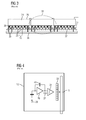
- FIG. 3 shows the basic construction of such counting detectors.
- X-ray radiation is converted in a direct converter 24 (for example CdTe or CZT) and the generated charge carrier pairs separated by an electrical field, which is generated by a shared top electrode 26 and a pixel electrode 25 .
- the charge In one of the pixel-like pixel electrodes 25 of the ASIC 27 the charge generates a charge pulse, the size of which corresponds to the energy of the X-ray quantum and which, if above a defined threshold value, is registered as a count event.
- the threshold value is used to distinguish an actual event from electronic noise or for example to also suppress k-fluorescence photons, in order to distinguish multiple counts.
- the ASIC 27 a corresponding section of the direct converter 24 and a coupling between direct converter 24 and ASIC 27 (in the case of directly-converting detectors for example by means of bump bonds 36 ) each form the detector module 35 having a large number of pixel elements 12 .
- the ASIC 27 is arranged on a substrate 37 and connected to peripheral electronic devices 38 .
- a detector module can also have one of more ASIC(s) and one or more parts of a direct converter, chosen as required in each case.
- FIG. 4 shows the general diagram of a counting pixel element.
- the electrical charge passes the charge input 28 , is collected in the pixel element and amplified there with the aid of a charge amplifier 29 and a feedback capacitor 40 .
- the pulse shape can also be adjusted at the output in a shaper (filter) (not shown).
- An event is then counted in that a digital storage unit (counter) 33 is incremented by one if the output signal lies above an adjustable threshold value. This is established by way of a discriminator 31 .
- the threshold value can in principle also be predetermined in a strictly analogue manner, but in general is applied across for example a DAC 32 (digital to analog converter) and can be variably adjusted in a certain region thereby.
- FIG. 5 shows a corresponding diagram for an entire array of counting pixel elements 12 , for example 100 ⁇ 100 pixel elements each of, for example, 180 ⁇ m. Such an array is implemented with the aid of the ASIC. In this example it has a size of 1.8 ⁇ 1.8 cm 2 .
- a plurality of detector modules 35 is combined (in this example 11 ⁇ 17 would produce roughly this area) and is connected by the shared peripheral electronic devices.
- TSV technology through silicon via
- two, three or more threshold values are introduced and the size of the charge pulse, corresponding to the predefined threshold values (discriminator thresholds), are classified in one or more of the digital storage unit(s) (counters).
- the X-ray quanta counted in a certain energy field may then be obtained by calculating the difference in the counter contents of two corresponding counters.
- the discriminators may be adjusted for example with the aid of DACs (digital-to-analog converter) for the whole detector module or pixel-by-pixel within given limits or ranges.
- the counter contents of the pixel elements are successively read module-by-module by a corresponding reading unit. This reading process requires a certain amount of time during which counting cannot continue without errors.
- an X-ray radiation window and a reading window must be defined as in the case of integrating detectors.
- a design of this kind which as in this example requires 1 ⁇ s reading time per pixel element, already reaches its limits at an image rate of 100 fps since the X-ray window then shrinks to 0 ms.
- the radiation process continues during the reading process and can consequently either not be counted (no use of the radiation dose) or, if this is not ruled out by the design, the count signals each correspond to slightly different periods of time, and this is something which should be avoided at all costs.
- Higher switching frequencies of for example 10 MHz can lower the reading time for the example detector module to 1 ms, but at 100 fps there is still a ratio of 1:9 between reading time and usable radiation time.
- One embodiment provides a counting digital X-ray detector for taking X-ray images of an object penetrated by X-ray radiation, having at least one detector module, the detector module having an X-ray converter for converting X-ray radiation into an electrical signal and a matrix having a large number of counting pixel elements, wherein each counting pixel element has a signal input, a conversion device for converting the electrical signal into a count signal and a first digital storage unit for storing the count signal, wherein exactly one second digital storage unit is allocated to each first storage unit and is designed to form a copy of the first storage unit at the moment of transfer by way of a transfer process, and wherein the X-ray detector is designed in such a way that the transfer process can be carried out simultaneously for the large number of pixel elements.
- the conversion device has a charge amplifier and at least one discriminator each with an adjustable threshold value.
- the conversion device has a plurality of discriminators each with different threshold values and the pixel element has a plurality of first digital storage units for counting count signals of different levels.
- the X-ray converter is formed by a direct converter, in particular CdTe.
- the X-ray detector has a large number of detector modules.
- the digital storage units are formed by counters.
- Another embodiment provides a method for taking a series of X-ray images of an object with a counting digital X-ray detector as disclosed above, wherein (a) X-ray radiation penetrating the object during an X-ray window is converted in a spatially resolved manner into electrical signals, (b) the electrical signals are converted pixel-by-pixel into count signals and are stored in the respective first storage units, (c) the stored count signals of all pixel elements are simultaneously transferred from the first storage units into the second storage units and then the first storage units are re-set to zero, (d) the contents of the second storage units are then sequentially read from the X-ray detector and the second storage units are re-set to zero, and (e) the steps are repeated several times in the sequence a to d, wherein steps a and b occur at least partially while step d of the preceding sequence is being carried out.
- FIG. 1 shows a view of a known X-ray system for use in interventional procedures
- FIG. 2 shows a view of a known X-ray detector with a scintillator
- FIG. 3 shows a plan view of a detail of a known X-ray detector with a plurality of detector modules
- FIG. 4 shows a diagram of the central functional elements of a counting pixel element of a known X-ray detector
- FIG. 5 shows a diagram of a matrix comprising counting pixel elements of a known X-ray detector with control and reading logic
- FIG. 6 shows a diagram of the central functional elements of a counting pixel element of an X-ray detector with a first and a second digital storage element, according to one embodiment of the invention
- FIG. 7 shows a diagram of the central functional elements of a counting, energy-discriminating pixel element of an X-ray detector having a plurality of first and second digital storage elements, according to one embodiment of the invention
- FIG. 8 shows a diagram of a matrix comprising counting pixel elements according to FIG. 7 of an X-ray detector, according to one embodiment of the invention
- FIG. 9 shows a synchronous timing diagram of a method with pulsed X-ray radiation, according to one embodiment of the invention.
- FIG. 10 shows an asynchronous timing diagram of a method with pulsed X-ray radiation, according to one embodiment of the invention.
- FIG. 11 shows an asynchronous timing diagram of a method with continuous X-ray radiation, according to one embodiment of the invention
- FIG. 12 shows a sequence of a method for compiling part images to form a corrected overall image
- FIG. 13 shows a further sequence of a method for compiling part images to form a corrected overall image
- FIG. 14 shows a diagram of the central functional elements of a counting, energy-discriminating pixel element having a discriminator with a plurality of threshold values.
- Embodiments of the present invention provide a counting digital X-ray detector which enables high frame rates with high image quality of X-ray images for interventional applications.
- Other embodiments provide a corresponding method for taking a series of X-ray images.
- One embodiment provides a counting digital X-ray detector for taking X-ray images of an object penetrated by X-ray radiation, having at least one detector module, comprising an X-ray converter for converting X-ray radiation into an electrical signal and a matrix comprising a large number of counting pixel elements, wherein each counting pixel element has a signal input, a conversion device for converting the electrical signal into a count signal and a first digital storage unit for storing the count signal, wherein exactly one second digital storage unit is allocated to each first storage unit, and this is designed to form a copy of the first storage unit at the moment of transfer by way of a transfer process, is designed in such a way that the transfer process is simultaneously carried out for the large number of pixel elements.
- the count contents of the first digital storage units can be transferred to the second digital storage units (“shadow storage devices”) within a very short time and for all pixel elements simultaneously, so the first storage units can be re-set to zero very quickly and are thereby free for new counting operations.
- the reading process which generally occurs sequentially and requires a relatively long time, can consequently be shifted to the second digital storage units.
- new X-ray radiation can again be evaluated very quickly and yet at the same time as the reading process and count signals can be stored in the first digital storage unit.
- the frame rate when taking series of X-ray images can thus be significantly increased and a high image quality retained in the process.
- the first digital storage unit can in particular be a counter with the task of both incrementing a count event with each electrical signal, which lies above a corresponding discriminator threshold value, and of storing the corresponding counter content.
- a digital register, shift register or sequential logic system for example can be used as a counter, and this is incremented by a count unit as soon as there is a logic pulse (here from the discriminator) at its input.
- the register is set to zero at the start of a count period.
- the counter can be read sequentially or simultaneously.
- the second digital storage unit can be a pure storage device which is capable of receiving and buffering a copy of the counter reading of the first digital storage unit. This storage device can also be a register which can be written on or read either sequentially or simultaneously.
- the conversion device has a charge amplifier and at least one discriminator each with an adjustable threshold value.
- the threshold value can be applied for example across a DAC. In this way only electrical signals which exceed the threshold value are counted, so noise can be faded out or only events with energies above a desired threshold are counted.
- Window discriminators can also be provided which have both a lower and an upper threshold value, so only events whose energy is above the lower threshold value and below the upper threshold value are counted in the corresponding counter.
- the upper threshold value can therefore be set for example such that it is not higher than the maximum expected X-ray energy.
- the conversion unit has a plurality of discriminators each with different threshold values and the pixel element has a plurality of first digital storage units for counting count signals of different levels.
- Each electrical signal is consequently classified in the corresponding first storage unit according to its signal level.
- Two, three, four or a large number of first storage units and threshold values may be provided.
- a corresponding number of second digital storage units is of course likewise provided.
- the X-ray converter is formed by a direct converter, in particular CdTe (cadmium telluride).
- CdTe cadmium telluride
- Other direct converter materials such as CZT (cadmium zinc telluride), HgI, PbO, etc. may also be used.
- Direct converters of this kind have the advantage of generating high electrical signals and count rates since the layer thicknesses may be much higher than for example in the case of indirect converters, so there is higher absorption. As a result, higher DQEs (Detective Quantum Efficiency) are in turn possible over the entire spatial frequency range.
- the X-ray detector advantageously has a large number of detector modules. Large-area X-ray detectors may thus be produced.
- the (first and second) digital storage units are expediently formed by counters.
- FIG. 6 shows the central functional elements of a pixel element of a digital counting X-ray detector, according to one embodiment of the invention.
- a second digital storage unit 41 (“shadow storage device”) is arranged in the pixel element.
- shadow storage device By way of a transfer process the content of the first digital storage unit is very quickly transferred into the second digital storage unit and a 1:1 copy of the first storage unit is generated in the second storage unit 41 .
- This may be easily carried out such that this transfer process occurs simultaneously for all pixel elements of a detector module or the entire X-ray detector. Depending on the architecture of the storage units this can be carried out successively bit for bit for each storage unit or for all bits simultaneously.
- Reading from the second storage units then occurs within the time window corresponding to the image frequencies (called counting intervals below) to enable the next transfer from the first storage unit to the second storage unit.
- this lasts 10 ms or 1 ms accordingly with a clock frequency of 1 MHz or 10 MHz (by way of simplification it is assumed that the transfer of an entire count content is possible within a clock cycle, i.e. all bits of a counter are read simultaneously; if this occurs sequentially, the time then increases in accordance with the bit depth of the counters and reduces the possible image frequencies accordingly).
- For a clock frequency of 1 MHz image rates of up to 100 fps and for 10 MHz image rates of up to 1,000 fps may therefore be achieved.
- FIG. 7 shows a further example for the central functional elements of a pixel element of a digital counting X-ray detectors, according to one embodiment of the invention.
- the pixel element 12 has a plurality of, for example four, first digital storage units 33 . 1 , 33 . 2 , 33 . 3 , 33 . 4 each with a DAC 32 . 1 , 32 . 2 , 32 . 3 , 32 . 4 with different threshold values.
- Energy-selective imaging can be carried out with a construction of this kind.
- One second digital storage unit 41 . 1 , 41 . 2 , 41 . 3 , 41 . 4 respectively is allocated to each first digital storage unit 33 . 1 , 33 . 2 , 33 .
- the contents of all first storage units can be simultaneously transferred as 1:1 copies to the second storage units for all pixel elements by way of a transfer process in this case as well.
- the first storage units can then be reset to zero and then be used further (written on) while the contents are being read from the second storage units.
- FIG. 8 shows a corresponding schematic diagram for an ASIC with counting pixel elements 12 as shown in FIG. 7 , for example 100 ⁇ 100 pixel elements.
- a detector module has one ASIC and a continuous piece of a direct converter.
- a detector module has a plurality of ASICs and/or a plurality of parts of a direct converter.
- FIG. 14 shows a further example of the central functional elements of a pixel element, operating energy-selectively, of a digital counting X-ray detector, according to one embodiment of the invention.
- the pixel element has one ADC (analog digital converter) 47 with successive approximation, i.e. with one discriminator 31 and one DAC 32 , wherein the DAC 32 successively generates the increasing threshold values V1 to V4 and successively applies them at the discriminator.
- the corresponding first digital storage element (1 to 4) is increased by one bit if the detector signal lies above the threshold value (1 to 4).
- the successive approximation logic 46 then ensures that the next higher threshold value is generated at the DAC 32 , and this is then again applied at the comparator.
- the ADC is started by moving a switch as soon as there is a signal at the discriminator which is higher than a start threshold value V0, which, in turn, must be lower than the first threshold value V1.
- One second digital storage unit 41 . 1 , 41 . 2 , 41 . 3 , 41 . 4 respectively is allocated to each first digital storage unit 33 . 1 , 33 . 2 , 33 . 3 , 33 . 4 .
- the contents of all first storage units can be simultaneously transferred as 1:1 copies to the second storage units for all pixel elements by way of a transfer process in this case as well.
- the digital storage units can be formed by what are known as counters.
- the counter depth depends on both the maximum expected count rate and the count time during which count signals are registered. If the count time, during which count signals accrue (hereinafter called “counting interval”), and the X-ray window can be fixed independently of each other, then additional degrees of freedom are obtained. Important free parameters are the transfer time (time for simultaneously (parallel) transferring the contents of the first storage units for all pixel elements into the second storage units), the (detector) module reading time, the X-ray window length (the time within which radiation is to be detected for a resulting X-ray image irrespective of whether pulsed or continuous radiation is applied) and the counting interval.
- the pixel matrix per detector module is for example 100 ⁇ 100 pixel elements.
- the X-ray window length is for example a minimum of 10 ms.
- the max. expected count rate is 30,000, so a counter bit depth of 15 bits is required.
- the maximum count rate is for example 500 Mcps/mm 2 and the pixel size 300*300 ⁇ m 2 . This corresponds therefore to about 45 Mcps per pixel element.
- the pixel matrix per detector module is for example 71*71 pixel elements (5,041 pixel elements per detector module).
- the in-pixel transfer time is for example about 20 ns (assumption: about 50 MHz clock rate and transfer of the content of the first storage units into the corresponding second storage units within a clock cycle), the module reading time is for example 100 ⁇ s (about 20 ns ⁇ 5,041 produces about 100 ⁇ s; assumption: all bits of the second storage unit of a pixel element are read simultaneously and within a clock cycle into the peripheral electronic devices) and the X-ray window length is for example a minimum of 2 ms.
- the counting interval which must be longer than the module reading time, is for example 200 ⁇ s (i.e. during the X-ray window the first storage unit is reset 10 times or transferred into the corresponding second storage unit).
- the maximum expected count rate is 45,000, from which a required bit depth of 16 bits follows.
- the maximum count rate is for example 50 Mcps/mm 2 . With a pixel size of 180*180 ⁇ m 2 these are slightly more than 1.6 Mcps per pixel element.
- the pixel matrix per detector module is for example 100 ⁇ 100 pixel elements.
- the maximum expected count rate is 300, from which a required bit depth of 9 bits follows.
- the maximum expected count rate is 3,000, so a counter bit depth of 12 bits is required.
- the counting interval is always at least as long as the module reading time, the module reading time is at most as long as the shortest X-ray window, the counter bit depth is deep enough to cover the highest count rates per pixel element and counting interval and the transfer time from the first storage unit into the second storage unit and the resetting time of the first storage unit are negligible with respect to a counting interval (for example 1% thereof or less).
- the content of the first storage unit is transferred into the second storage unit within a switching interval (data transfer within the pixel element) or the content of the second storage unit of each pixel element is also transferred to the peripheral electronic devices of the X-ray detectors when the detector module is read. If the bit contents are transferred sequentially instead of simultaneously for example, the respective transfer takes longer accordingly (i.e. with an 8 bit counter, 8 times as long for example). Depending on the definition or implementation a plurality of switching intervals could also be necessary to carry out certain ASIC operations such as the transfer of bit contents from one storage device into another. The transfer or reading times are then correspondingly longer.
- the examples should, however, only be used to highlight the general dependencies of the various design definitions on each other and on the application boundary conditions.
- the second storage units may also be read simultaneously or sequentially.
- the following cases are conceivable: (1) completely simultaneously: all bits of all first storage devices of a pixel element are simultaneously transferred into the corresponding bits of the second storage devices of the pixel element, (2) semi-simultaneously: simultaneously for all first storage devices of a pixel element, but the contents are transferred bit for bit into the corresponding second storage devices, (3) completely sequentially: the bits are transferred sequentially and successively for the various first storage devices into the corresponding bits of the second storage device (this is the longest variant timewise but also the one with the fewest parallel connections).
- Reading of all detector modules will hereinafter be called “reading”.
- Data or image pre-processing can occur in the peripheral electronic devices, thus for example the compiling of the detector module readings to form an overall reading of all detector modules.
- each reading could be depicted as an image.
- a plurality of readings i.e. for example all readings which occur during the X-ray window length
- a plurality of readings are compiled to form an image by adding all count signals. If a plurality of first and second storage units per pixel element are a component of the design, then a plurality of images (for example 4) result in accordance with the contents of the various storage units (for example FIG. 7 ).
- the X-ray window length matches the inverse image frequency since no dead times accrue due to the reading process.
- the various readings can be compiled to form an image. This can either be carried out in the X-ray detector or externally before actual image processing.
- the advantages of the disclosed X-ray detector are inter alia as follows: significant degrees of design and application freedom result since the taking and reading processes are separated from each other in actuality. Continuous X-ray radiation may also be used (in particular for high-end 3 D applications (flat-panel volume CT), without significant dead times (radiation without detection) occurring.
- the bit depths of the digital storage units (counters) can be optimized (i.e. reduced to the smallest possible size). The space requirement on each pixel element is consequently lower (one counting pixel element may require hundreds to well over 1,000 transistors depending on design). Smaller counter structures results in space on the pixel element for other functions.
- FIGS. 9 to 11 show some examples of a course over time of the method, wherein FIG. 9 shows synchronous counting and reading and FIGS. 10 and 11 show asynchronous counting and reading.
- FIG. 9 shows synchronous control, wherein the start and end of the respective X-ray window (three X-ray windows 42 are shown) triggers the readings (four per X-ray pulse are shown here).
- the four counting intervals 43 per X-ray pulse during which count signals are respectively stored in the first storage units are shown under B).
- the instant of the transfer operation from the first storage units to the second storage units and the resetting of the first storage units is shown under C), wherein a very short transfer time 44 is assumed.
- the first storage units can be written on again directly thereafter.
- the module reading times 45 during which the second storage units are read are shown under D). Images are then compiled from various readings, for example from all readings of an X-ray pulse.
- FIG. 10 shows asynchronous control.
- asynchronous control between generator/X-ray tube and X-ray detector and pulsed X-ray radiation a plurality of readings with count content alternate with ones without count content (if the counting interval is small compared with pulse time and non-radiation time). Images pertaining to the corresponding pulses can then be generated in that averaged readings are added to an image until a reading without a count content appears. The next image is generated as soon as a reading with a count content appears again—corresponding to the next X-ray pulse.
- FIG. 11 shows asynchronous control with continuous X-ray radiation.
- a certain number of readings can be defined which are allocated to one image.
- FIGS. 12 and 13 show two of several possibilities as to how an image can be compiled from the individual readings of a plurality of different detector modules to arrive at an artifact-free flat image.
- the ASIC design is similar in this case but photodiodes are necessary.
- one or more optical coupling layer(s) are necessary between the indirect converter material (scintillator) and counting ASIC for example.
- aspects of the invention may also be used for other fields of application, such as radiography, mammography or computerized tomography.
- a counting digital X-ray detector for taking X-ray images of an object penetrated by X-ray radiation, having at least one detector module
- the detector module comprising a X-ray converter for converting X-ray radiation into an electrical signal and a matrix having a large number of counting pixel elements, wherein each counting pixel element has a signal input, a conversion device for converting the electrical signal into a count signal and a first digital storage unit for storing the count signal, wherein exactly one second digital storage unit is allocated to each first storage unit, and this is designed to form a copy of the first storage unit at the moment of transfer by way of a transfer process, and wherein the X-ray detector is designed such that the transfer process can be simultaneously carried out for the large number of pixel elements.
Abstract
Description
- a) X-ray radiation penetrating the object during an X-ray window is converted in a spatially resolved manner into electrical signals,
- b) the electrical signals are converted pixel-by-pixel into count signals and are stored in the respective first storage units,
- c) the stored count signals of all pixel elements are simultaneously transferred from the first storage units into the second storage units and then the first storage units are re-set to zero,
- d) the contents of the second storage units are then sequentially read from the X-ray detector and the second storage units are re-set to zero, and
- e) the steps are repeated several times in the sequence a to d, wherein steps a and b occur at least partially while step d of the preceding sequence is being carried out.
Claims (18)
Applications Claiming Priority (3)
| Application Number | Priority Date | Filing Date | Title |
|---|---|---|---|
| DE102012212124.2 | 2012-07-11 | ||
| DE102012212124.2A DE102012212124B4 (en) | 2012-07-11 | 2012-07-11 | Counting digital x-ray detector and method of capturing a series of x-ray images |
| DE102012212124 | 2012-07-11 |
Publications (2)
| Publication Number | Publication Date |
|---|---|
| US20140016748A1 US20140016748A1 (en) | 2014-01-16 |
| US9417339B2 true US9417339B2 (en) | 2016-08-16 |
Family
ID=49781492
Family Applications (1)
| Application Number | Title | Priority Date | Filing Date |
|---|---|---|---|
| US13/939,925 Active 2034-03-19 US9417339B2 (en) | 2012-07-11 | 2013-07-11 | Counting digital X-ray detector and method for taking a series of X-ray images |
Country Status (2)
| Country | Link |
|---|---|
| US (1) | US9417339B2 (en) |
| DE (1) | DE102012212124B4 (en) |
Cited By (21)
| Publication number | Priority date | Publication date | Assignee | Title |
|---|---|---|---|---|
| US20140185765A1 (en) * | 2012-12-27 | 2014-07-03 | Samsung Electronics Co., Ltd. | X-ray detection panel, x-ray imaging apparatus, and x-ray image generation method |
| US20150131776A1 (en) * | 2013-11-12 | 2015-05-14 | Samsung Electronics Co., Ltd. | Radiation detector and computed tomography apparatus using the same |
| US20150250444A1 (en) * | 2014-03-05 | 2015-09-10 | Kabushiki Kaisha Toshiba | Photon counting ct apparatus |
| US20150282778A1 (en) * | 2012-12-27 | 2015-10-08 | Kabushiki Kaisha Toshiba | X-ray ct apparatus and controlling method |
| US20160022243A1 (en) * | 2013-04-04 | 2016-01-28 | Kabushiki Kaisha Toshiba | X-ray computed tomography apparatus |
| US20160045176A1 (en) * | 2013-04-26 | 2016-02-18 | Kabushiki Kaisha Toshiba | Photon counting ct apparatus, light detection device, radiation detection device, and radiation analysis device |
| US20160095564A1 (en) * | 2014-10-01 | 2016-04-07 | Kabushiki Kaisha Toshiba | X-ray ct apparatus, image processing apparatus, and image processing method |
| US20160157799A1 (en) * | 2014-12-05 | 2016-06-09 | Samsung Electronics Co., Ltd. | Computed tomographic apparatus and method for controlling the same |
| US20170020475A1 (en) * | 2015-07-23 | 2017-01-26 | Martin Spahn | X-ray image generation |
| US20170035376A1 (en) * | 2015-08-06 | 2017-02-09 | Texas Instruments Incorporated | Low power photon counting system |
| US20170086761A1 (en) * | 2015-09-29 | 2017-03-30 | General Electric Company | Apparatus and method for pile-up correction in photon-counting detector |
| US20170090039A1 (en) * | 2015-09-30 | 2017-03-30 | General Electric Company | Layered radiation detector |
| US20170227658A1 (en) * | 2014-10-31 | 2017-08-10 | Koninklijke Philips N.V. | Sensor device and imaging system for detecting radiation signals |
| US20170269008A1 (en) * | 2015-11-12 | 2017-09-21 | Prismatic Sensors Ab | High-resolution computed tomography using edge-on detectors with temporally offset depth-segments |
| US10024979B1 (en) | 2017-11-01 | 2018-07-17 | Texas Instruments Incorporated | Photon counting with coincidence detection |
| US10151845B1 (en) | 2017-08-02 | 2018-12-11 | Texas Instruments Incorporated | Configurable analog-to-digital converter and processing for photon counting |
| US10211844B1 (en) * | 2018-01-24 | 2019-02-19 | Futurewei Technologies, Inc. | Minimum search length analog to digital converter |
| US20190154852A1 (en) * | 2017-11-16 | 2019-05-23 | NueVue Solutions, Inc. | Analog Direct Digital X-Ray Photon Counting Detector For Resolving Photon Energy In Spectral X-Ray CT |
| US20190204243A1 (en) * | 2017-12-28 | 2019-07-04 | Tsinghua University | Ct inspection system and ct imaging method |
| US20200155110A1 (en) * | 2018-11-16 | 2020-05-21 | Varex Imaging Corporation | Imaging system with energy sensing and method for operation |
| US10890674B2 (en) | 2019-01-15 | 2021-01-12 | Texas Instruments Incorporated | Dynamic noise shaping in a photon counting system |
Families Citing this family (16)
| Publication number | Priority date | Publication date | Assignee | Title |
|---|---|---|---|---|
| DE102013200021B4 (en) * | 2013-01-02 | 2016-01-28 | Siemens Aktiengesellschaft | Method for calibrating a counting digital X-ray detector, X-ray systems for carrying out such a method and method for recording an X-ray image |
| DE102013218692B4 (en) | 2013-09-18 | 2022-09-08 | Siemens Healthcare Gmbh | Detection of X-ray radiation |
| DE102013219740A1 (en) | 2013-09-30 | 2015-04-02 | Siemens Aktiengesellschaft | Counting digital X-ray image detector with two switchable modes |
| KR101635980B1 (en) * | 2013-12-30 | 2016-07-05 | 삼성전자주식회사 | Radiation detector and computer tomography apparatus thereof |
| WO2015105314A1 (en) * | 2014-01-07 | 2015-07-16 | Samsung Electronics Co., Ltd. | Radiation detector, tomography imaging apparatus thereof, and radiation detecting apparatus thereof |
| CN106688309B (en) | 2014-09-12 | 2019-08-09 | 飞利浦照明控股有限公司 | LED dimmer circuit and method |
| EP3320371A4 (en) * | 2015-06-10 | 2019-03-06 | Shenzhen Xpectvision Technology Co., Ltd. | A detector for x-ray fluorescence |
| DE102015212155A1 (en) | 2015-06-30 | 2017-01-05 | Siemens Healthcare Gmbh | Method for recording energy-selective image data, X-ray detector and X-ray system |
| CN106716178B (en) * | 2015-07-09 | 2021-06-22 | 皇家飞利浦有限公司 | Direct conversion radiation detector |
| DE102015218581B4 (en) * | 2015-09-28 | 2019-11-14 | Siemens Healthcare Gmbh | Digital-to-analogue converter for multi-threshold counters with partitioning of the bits between R-conductor and comparator |
| CN108027448B (en) * | 2015-10-09 | 2022-02-11 | 深圳帧观德芯科技有限公司 | Packaging method of semiconductor X-ray detector |
| WO2017216378A1 (en) * | 2016-06-16 | 2017-12-21 | Koninklijke Philips N.V. | Improved photon-counting in a spectral radiation detector |
| JP7146424B2 (en) * | 2018-03-19 | 2022-10-04 | キヤノン株式会社 | Photoelectric conversion device and imaging system |
| TWI750713B (en) * | 2020-06-24 | 2021-12-21 | 茂達電子股份有限公司 | Rapid sensing value estimation circuit and method thereof |
| DE102020210957A1 (en) * | 2020-08-31 | 2022-03-03 | Siemens Healthcare Gmbh | Evaluation unit for an X-ray detector, X-ray detector, medical imaging device and method for operating an X-ray detector |
| US11911197B2 (en) * | 2021-12-14 | 2024-02-27 | BAE Systems Imaging Solutions Inc. | X-ray sensor system for intraoral tomography |
Citations (9)
| Publication number | Priority date | Publication date | Assignee | Title |
|---|---|---|---|---|
| US6248990B1 (en) | 1996-10-15 | 2001-06-19 | Simage Oy | Radiation imaging device with an array of image cells |
| US20070005278A1 (en) * | 2003-05-14 | 2007-01-04 | Brunnett Carl J | Method and apparatus for improved radiation detection |
| DE102005060310A1 (en) | 2005-12-16 | 2007-06-21 | Siemens Ag | X ray detection procedure applies X rays during successive time windows with overlap on preceding read out period |
| US7332724B2 (en) | 2005-07-26 | 2008-02-19 | General Electric Company | Method and apparatus for acquiring radiation data |
| US20090290680A1 (en) | 2004-03-26 | 2009-11-26 | Nova R & D, Inc. | High resolution imaging system |
| US20090302232A1 (en) * | 2006-03-22 | 2009-12-10 | Ii-Vi Incorporated | Multi-window signal processing electronics architecture for photon counting with multi-element sensors |
| US20110210235A1 (en) * | 2009-02-25 | 2011-09-01 | Bart Dierickx | Photon sharpening |
| US20130228693A1 (en) * | 2012-03-02 | 2013-09-05 | Luxen Technologies, Inc. | Parallel readout integrated circuit architecture for x-ray image sensor |
| US20130341521A1 (en) * | 2012-06-21 | 2013-12-26 | Honeywell International Inc. | Integrated comparative radiation sensitive circuit |
-
2012
- 2012-07-11 DE DE102012212124.2A patent/DE102012212124B4/en not_active Expired - Fee Related
-
2013
- 2013-07-11 US US13/939,925 patent/US9417339B2/en active Active
Patent Citations (12)
| Publication number | Priority date | Publication date | Assignee | Title |
|---|---|---|---|---|
| US6248990B1 (en) | 1996-10-15 | 2001-06-19 | Simage Oy | Radiation imaging device with an array of image cells |
| DE69711902T2 (en) | 1996-10-15 | 2002-11-14 | Simage Oy Espoo | RADIATION IMAGE RECORDING DEVICE |
| US20070005278A1 (en) * | 2003-05-14 | 2007-01-04 | Brunnett Carl J | Method and apparatus for improved radiation detection |
| US20090290680A1 (en) | 2004-03-26 | 2009-11-26 | Nova R & D, Inc. | High resolution imaging system |
| US7332724B2 (en) | 2005-07-26 | 2008-02-19 | General Electric Company | Method and apparatus for acquiring radiation data |
| DE112006001859T5 (en) | 2005-07-26 | 2008-05-29 | Ge Medical Systems Israel, Ltd. | Method and device for acquiring radiation data |
| DE102005060310A1 (en) | 2005-12-16 | 2007-06-21 | Siemens Ag | X ray detection procedure applies X rays during successive time windows with overlap on preceding read out period |
| US7470910B2 (en) | 2005-12-16 | 2008-12-30 | Siemens Aktiengesellschaft | Method and X ray detector |
| US20090302232A1 (en) * | 2006-03-22 | 2009-12-10 | Ii-Vi Incorporated | Multi-window signal processing electronics architecture for photon counting with multi-element sensors |
| US20110210235A1 (en) * | 2009-02-25 | 2011-09-01 | Bart Dierickx | Photon sharpening |
| US20130228693A1 (en) * | 2012-03-02 | 2013-09-05 | Luxen Technologies, Inc. | Parallel readout integrated circuit architecture for x-ray image sensor |
| US20130341521A1 (en) * | 2012-06-21 | 2013-12-26 | Honeywell International Inc. | Integrated comparative radiation sensitive circuit |
Non-Patent Citations (1)
| Title |
|---|
| Spahn, Martin, "Flat Detectors and Their Clinical Applications," Eur Radiol, vol. 15, 14 pages, Mar. 1, 2005. |
Cited By (41)
| Publication number | Priority date | Publication date | Assignee | Title |
|---|---|---|---|---|
| US9901318B2 (en) * | 2012-12-27 | 2018-02-27 | Samsung Electronics Co., Ltd. | X-ray detection panel, X-ray imaging apparatus, and X-ray image generation method |
| US20140185765A1 (en) * | 2012-12-27 | 2014-07-03 | Samsung Electronics Co., Ltd. | X-ray detection panel, x-ray imaging apparatus, and x-ray image generation method |
| US20150282778A1 (en) * | 2012-12-27 | 2015-10-08 | Kabushiki Kaisha Toshiba | X-ray ct apparatus and controlling method |
| US9924916B2 (en) * | 2012-12-27 | 2018-03-27 | Toshiba Medical Systems Corporation | X-ray CT apparatus and controlling method |
| US10182775B2 (en) * | 2013-04-04 | 2019-01-22 | Toshiba Medical Systems Corporation | X-ray computed tomography apparatus including a first X-ray detector and a second X-ray detector for counting X-ray photons |
| US20160022243A1 (en) * | 2013-04-04 | 2016-01-28 | Kabushiki Kaisha Toshiba | X-ray computed tomography apparatus |
| US20160045176A1 (en) * | 2013-04-26 | 2016-02-18 | Kabushiki Kaisha Toshiba | Photon counting ct apparatus, light detection device, radiation detection device, and radiation analysis device |
| US10357214B2 (en) * | 2013-04-26 | 2019-07-23 | Toshiba Medical Systems Corporation | Photon counting CT apparatus, light detection device, radiation detection device, and radiation analysis device |
| US20150131776A1 (en) * | 2013-11-12 | 2015-05-14 | Samsung Electronics Co., Ltd. | Radiation detector and computed tomography apparatus using the same |
| US10751009B2 (en) | 2013-11-12 | 2020-08-25 | Samsung Electronics Co., Ltd. | Radiation detector and computed tomography apparatus using the same |
| US9986957B2 (en) * | 2013-11-12 | 2018-06-05 | Samsung Electronics Co., Ltd. | Radiation detector and computed tomography apparatus using the same |
| US20150250444A1 (en) * | 2014-03-05 | 2015-09-10 | Kabushiki Kaisha Toshiba | Photon counting ct apparatus |
| US9867590B2 (en) * | 2014-03-05 | 2018-01-16 | Toshiba Medical Systems Corporation | Photon-counting CT apparatus |
| US10159450B2 (en) * | 2014-10-01 | 2018-12-25 | Toshiba Medical Systems Corporation | X-ray CT apparatus including a photon-counting detector, and an image processing apparatus and an image processing method for correcting detection signals detected by the photon-counting detector |
| US20160095564A1 (en) * | 2014-10-01 | 2016-04-07 | Kabushiki Kaisha Toshiba | X-ray ct apparatus, image processing apparatus, and image processing method |
| US20170227658A1 (en) * | 2014-10-31 | 2017-08-10 | Koninklijke Philips N.V. | Sensor device and imaging system for detecting radiation signals |
| US9955930B2 (en) * | 2014-10-31 | 2018-05-01 | Koninklijke Philips N.V. | Sensor device and imaging system for detecting radiation signals |
| US20160157799A1 (en) * | 2014-12-05 | 2016-06-09 | Samsung Electronics Co., Ltd. | Computed tomographic apparatus and method for controlling the same |
| US10357215B2 (en) * | 2014-12-05 | 2019-07-23 | Samsung Electronics Co., Ltd. | Computed tomographic apparatus and method for controlling the same |
| US10448914B2 (en) * | 2015-07-23 | 2019-10-22 | Siemens Healthcare Gmbh | X-ray image generation |
| US20170020475A1 (en) * | 2015-07-23 | 2017-01-26 | Martin Spahn | X-ray image generation |
| US10098595B2 (en) * | 2015-08-06 | 2018-10-16 | Texas Instruments Incorporated | Low power photon counting system |
| US20170035376A1 (en) * | 2015-08-06 | 2017-02-09 | Texas Instruments Incorporated | Low power photon counting system |
| US20170086761A1 (en) * | 2015-09-29 | 2017-03-30 | General Electric Company | Apparatus and method for pile-up correction in photon-counting detector |
| US10117626B2 (en) * | 2015-09-29 | 2018-11-06 | General Electric Company | Apparatus and method for pile-up correction in photon-counting detector |
| US10646176B2 (en) * | 2015-09-30 | 2020-05-12 | General Electric Company | Layered radiation detector |
| US20170090039A1 (en) * | 2015-09-30 | 2017-03-30 | General Electric Company | Layered radiation detector |
| US20170269008A1 (en) * | 2015-11-12 | 2017-09-21 | Prismatic Sensors Ab | High-resolution computed tomography using edge-on detectors with temporally offset depth-segments |
| US10271803B2 (en) * | 2015-11-12 | 2019-04-30 | Prismatic Sensors Ab | High-resolution computed tomography using edge-on detectors with temporally offset depth-segments |
| US10481283B2 (en) | 2017-08-02 | 2019-11-19 | Texas Instruments Incorporated | Configurable analog-to-digital converter and processing for photon counting |
| US10151845B1 (en) | 2017-08-02 | 2018-12-11 | Texas Instruments Incorporated | Configurable analog-to-digital converter and processing for photon counting |
| US10024979B1 (en) | 2017-11-01 | 2018-07-17 | Texas Instruments Incorporated | Photon counting with coincidence detection |
| US20190154852A1 (en) * | 2017-11-16 | 2019-05-23 | NueVue Solutions, Inc. | Analog Direct Digital X-Ray Photon Counting Detector For Resolving Photon Energy In Spectral X-Ray CT |
| US20190204243A1 (en) * | 2017-12-28 | 2019-07-04 | Tsinghua University | Ct inspection system and ct imaging method |
| US10935691B2 (en) * | 2017-12-28 | 2021-03-02 | Tsinghua University | CT inspection system and CT imaging method for obtaining detection data at a frequency that is N times a beam-emitting frequency of a radioactive source device |
| US10211844B1 (en) * | 2018-01-24 | 2019-02-19 | Futurewei Technologies, Inc. | Minimum search length analog to digital converter |
| WO2019144890A1 (en) * | 2018-01-24 | 2019-08-01 | Huawei Technologies Co., Ltd. | Minimum search length analog to digital converter |
| US20200155110A1 (en) * | 2018-11-16 | 2020-05-21 | Varex Imaging Corporation | Imaging system with energy sensing and method for operation |
| US11071514B2 (en) * | 2018-11-16 | 2021-07-27 | Varex Imaging Corporation | Imaging system with energy sensing and method for operation |
| US10890674B2 (en) | 2019-01-15 | 2021-01-12 | Texas Instruments Incorporated | Dynamic noise shaping in a photon counting system |
| US11493649B2 (en) | 2019-01-15 | 2022-11-08 | Texas Instruments Incorporated | Dynamic noise shaping in a photon counting system |
Also Published As
| Publication number | Publication date |
|---|---|
| DE102012212124B4 (en) | 2018-06-14 |
| DE102012212124A1 (en) | 2014-01-16 |
| US20140016748A1 (en) | 2014-01-16 |
Similar Documents
| Publication | Publication Date | Title |
|---|---|---|
| US9417339B2 (en) | Counting digital X-ray detector and method for taking a series of X-ray images | |
| US9599730B2 (en) | Counting digital X-ray detector and method for recording an X-ray image | |
| US7573038B2 (en) | Radiation image pickup apparatus, radiation image pickup system, their control method and their control program | |
| US9931092B2 (en) | Radiation imaging system and operation method thereof, and radiation image detecting device and storage medium storing operation program therefor | |
| US7696483B2 (en) | High DQE photon counting detector using statistical recovery of pile-up events | |
| US10074679B2 (en) | Radiation image detecting device | |
| US10473798B2 (en) | Counting and integrating pixels, detectors, and methods | |
| US20060188061A1 (en) | Radiography apparatus, radiography system, and control method thereof | |
| US20140270073A1 (en) | Method and System for Acquiring an X-Ray Image | |
| US11313980B2 (en) | Radiation detection apparatus | |
| WO2014125888A1 (en) | X-ray computed tomography apparatus, and photon counting method | |
| US7127031B2 (en) | Radiation imaging apparatus, radiation imaging system and radiation imaging method | |
| US7657001B2 (en) | Method for reducing 3D ghost artefacts in an x-ray detector | |
| US8076646B2 (en) | Burst-mode readout for solid state radiation detectors using partitioned pipeline architecture | |
| US8634516B2 (en) | Energy subtraction imaging system, X-ray imaging apparatus, and computer readable recording medium | |
| JP6352084B2 (en) | Photon counting CT system | |
| CN115427839A (en) | Total time-to-over-threshold (TTOT) processing for photon counting X-ray detectors | |
| WO2016194315A1 (en) | Radiation imaging apparatus, control method therefor, and storage medium | |
| US10426415B2 (en) | Method for receiving energy -selective image data, X-ray detector and X-ray system | |
| JP2018139760A (en) | X-ray imaging apparatus | |
| EP3756033B1 (en) | Method of reading out data in a radiation detector, radiation detector and imaging apparatus | |
| US7589325B2 (en) | Method for recording a digital x-ray image, counting x-ray detector and x-ray system | |
| WO2019213755A1 (en) | Method and apparatus for a high resolution, high speed radiation imaging | |
| US9285486B2 (en) | Method for radiation detection signal processing | |
| EP4325254A1 (en) | Readout circuit, radiation detector, imaging apparatus and method of handling incident radiation |
Legal Events
| Date | Code | Title | Description |
|---|---|---|---|
| AS | Assignment |
Owner name: SIEMENS AKTIENGESELLSCHAFT, GERMANY Free format text: ASSIGNMENT OF ASSIGNORS INTEREST;ASSIGNOR:SPAHN, MARTIN;REEL/FRAME:037594/0701 Effective date: 20130821 |
|
| STCF | Information on status: patent grant |
Free format text: PATENTED CASE |
|
| AS | Assignment |
Owner name: SIEMENS HEALTHCARE GMBH, GERMANY Free format text: ASSIGNMENT OF ASSIGNORS INTEREST;ASSIGNOR:SIEMENS AKTIENGESELLSCHAFT;REEL/FRAME:040656/0054 Effective date: 20161104 |
|
| MAFP | Maintenance fee payment |
Free format text: PAYMENT OF MAINTENANCE FEE, 4TH YEAR, LARGE ENTITY (ORIGINAL EVENT CODE: M1551); ENTITY STATUS OF PATENT OWNER: LARGE ENTITY Year of fee payment: 4 |
|
| AS | Assignment |
Owner name: SIEMENS HEALTHINEERS AG, GERMANY Free format text: ASSIGNMENT OF ASSIGNORS INTEREST;ASSIGNOR:SIEMENS HEALTHCARE GMBH;REEL/FRAME:066088/0256 Effective date: 20231219 |
|
| MAFP | Maintenance fee payment |
Free format text: PAYMENT OF MAINTENANCE FEE, 8TH YEAR, LARGE ENTITY (ORIGINAL EVENT CODE: M1552); ENTITY STATUS OF PATENT OWNER: LARGE ENTITY Year of fee payment: 8 |