WO2010035644A1 - 半導体レーザ装置および表示装置 - Google Patents
半導体レーザ装置および表示装置 Download PDFInfo
- Publication number
- WO2010035644A1 WO2010035644A1 PCT/JP2009/065893 JP2009065893W WO2010035644A1 WO 2010035644 A1 WO2010035644 A1 WO 2010035644A1 JP 2009065893 W JP2009065893 W JP 2009065893W WO 2010035644 A1 WO2010035644 A1 WO 2010035644A1
- Authority
- WO
- WIPO (PCT)
- Prior art keywords
- semiconductor laser
- laser element
- layer
- green
- blue
- Prior art date
- Legal status (The legal status is an assumption and is not a legal conclusion. Google has not performed a legal analysis and makes no representation as to the accuracy of the status listed.)
- Ceased
Links
Images










Classifications
-
- H—ELECTRICITY
- H01—ELECTRIC ELEMENTS
- H01S—DEVICES USING THE PROCESS OF LIGHT AMPLIFICATION BY STIMULATED EMISSION OF RADIATION [LASER] TO AMPLIFY OR GENERATE LIGHT; DEVICES USING STIMULATED EMISSION OF ELECTROMAGNETIC RADIATION IN WAVE RANGES OTHER THAN OPTICAL
- H01S5/00—Semiconductor lasers
- H01S5/40—Arrangement of two or more semiconductor lasers, not provided for in groups H01S5/02 - H01S5/30
- H01S5/4025—Array arrangements, e.g. constituted by discrete laser diodes or laser bar
- H01S5/4031—Edge-emitting structures
-
- B—PERFORMING OPERATIONS; TRANSPORTING
- B82—NANOTECHNOLOGY
- B82Y—SPECIFIC USES OR APPLICATIONS OF NANOSTRUCTURES; MEASUREMENT OR ANALYSIS OF NANOSTRUCTURES; MANUFACTURE OR TREATMENT OF NANOSTRUCTURES
- B82Y20/00—Nanooptics, e.g. quantum optics or photonic crystals
-
- H—ELECTRICITY
- H01—ELECTRIC ELEMENTS
- H01S—DEVICES USING THE PROCESS OF LIGHT AMPLIFICATION BY STIMULATED EMISSION OF RADIATION [LASER] TO AMPLIFY OR GENERATE LIGHT; DEVICES USING STIMULATED EMISSION OF ELECTROMAGNETIC RADIATION IN WAVE RANGES OTHER THAN OPTICAL
- H01S5/00—Semiconductor lasers
- H01S5/30—Structure or shape of the active region; Materials used for the active region
- H01S5/32—Structure or shape of the active region; Materials used for the active region comprising PN junctions, e.g. hetero- or double- heterostructures
- H01S5/3202—Structure or shape of the active region; Materials used for the active region comprising PN junctions, e.g. hetero- or double- heterostructures grown on specifically orientated substrates, or using orientation dependent growth
- H01S5/320275—Structure or shape of the active region; Materials used for the active region comprising PN junctions, e.g. hetero- or double- heterostructures grown on specifically orientated substrates, or using orientation dependent growth semi-polar orientation
-
- H—ELECTRICITY
- H04—ELECTRIC COMMUNICATION TECHNIQUE
- H04N—PICTORIAL COMMUNICATION, e.g. TELEVISION
- H04N9/00—Details of colour television systems
- H04N9/12—Picture reproducers
- H04N9/31—Projection devices for colour picture display, e.g. using electronic spatial light modulators [ESLM]
- H04N9/3141—Constructional details thereof
- H04N9/315—Modulator illumination systems
- H04N9/3161—Modulator illumination systems using laser light sources
-
- H—ELECTRICITY
- H01—ELECTRIC ELEMENTS
- H01S—DEVICES USING THE PROCESS OF LIGHT AMPLIFICATION BY STIMULATED EMISSION OF RADIATION [LASER] TO AMPLIFY OR GENERATE LIGHT; DEVICES USING STIMULATED EMISSION OF ELECTROMAGNETIC RADIATION IN WAVE RANGES OTHER THAN OPTICAL
- H01S5/00—Semiconductor lasers
- H01S5/02—Structural details or components not essential to laser action
- H01S5/0206—Substrates, e.g. growth, shape, material, removal or bonding
- H01S5/0215—Bonding to the substrate
- H01S5/0216—Bonding to the substrate using an intermediate compound, e.g. a glue or solder
-
- H—ELECTRICITY
- H01—ELECTRIC ELEMENTS
- H01S—DEVICES USING THE PROCESS OF LIGHT AMPLIFICATION BY STIMULATED EMISSION OF RADIATION [LASER] TO AMPLIFY OR GENERATE LIGHT; DEVICES USING STIMULATED EMISSION OF ELECTROMAGNETIC RADIATION IN WAVE RANGES OTHER THAN OPTICAL
- H01S5/00—Semiconductor lasers
- H01S5/02—Structural details or components not essential to laser action
- H01S5/022—Mountings; Housings
- H01S5/0233—Mounting configuration of laser chips
- H01S5/0234—Up-side down mountings, e.g. Flip-chip, epi-side down mountings or junction down mountings
-
- H—ELECTRICITY
- H01—ELECTRIC ELEMENTS
- H01S—DEVICES USING THE PROCESS OF LIGHT AMPLIFICATION BY STIMULATED EMISSION OF RADIATION [LASER] TO AMPLIFY OR GENERATE LIGHT; DEVICES USING STIMULATED EMISSION OF ELECTROMAGNETIC RADIATION IN WAVE RANGES OTHER THAN OPTICAL
- H01S5/00—Semiconductor lasers
- H01S5/02—Structural details or components not essential to laser action
- H01S5/022—Mountings; Housings
- H01S5/0233—Mounting configuration of laser chips
- H01S5/02345—Wire-bonding
-
- H—ELECTRICITY
- H01—ELECTRIC ELEMENTS
- H01S—DEVICES USING THE PROCESS OF LIGHT AMPLIFICATION BY STIMULATED EMISSION OF RADIATION [LASER] TO AMPLIFY OR GENERATE LIGHT; DEVICES USING STIMULATED EMISSION OF ELECTROMAGNETIC RADIATION IN WAVE RANGES OTHER THAN OPTICAL
- H01S5/00—Semiconductor lasers
- H01S5/02—Structural details or components not essential to laser action
- H01S5/022—Mountings; Housings
- H01S5/0235—Method for mounting laser chips
- H01S5/02355—Fixing laser chips on mounts
- H01S5/0237—Fixing laser chips on mounts by soldering
-
- H—ELECTRICITY
- H01—ELECTRIC ELEMENTS
- H01S—DEVICES USING THE PROCESS OF LIGHT AMPLIFICATION BY STIMULATED EMISSION OF RADIATION [LASER] TO AMPLIFY OR GENERATE LIGHT; DEVICES USING STIMULATED EMISSION OF ELECTROMAGNETIC RADIATION IN WAVE RANGES OTHER THAN OPTICAL
- H01S5/00—Semiconductor lasers
- H01S5/20—Structure or shape of the semiconductor body to guide the optical wave ; Confining structures perpendicular to the optical axis, e.g. index or gain guiding, stripe geometry, broad area lasers, gain tailoring, transverse or lateral reflectors, special cladding structures, MQW barrier reflection layers
- H01S5/22—Structure or shape of the semiconductor body to guide the optical wave ; Confining structures perpendicular to the optical axis, e.g. index or gain guiding, stripe geometry, broad area lasers, gain tailoring, transverse or lateral reflectors, special cladding structures, MQW barrier reflection layers having a ridge or stripe structure
- H01S5/2201—Structure or shape of the semiconductor body to guide the optical wave ; Confining structures perpendicular to the optical axis, e.g. index or gain guiding, stripe geometry, broad area lasers, gain tailoring, transverse or lateral reflectors, special cladding structures, MQW barrier reflection layers having a ridge or stripe structure in a specific crystallographic orientation
-
- H—ELECTRICITY
- H01—ELECTRIC ELEMENTS
- H01S—DEVICES USING THE PROCESS OF LIGHT AMPLIFICATION BY STIMULATED EMISSION OF RADIATION [LASER] TO AMPLIFY OR GENERATE LIGHT; DEVICES USING STIMULATED EMISSION OF ELECTROMAGNETIC RADIATION IN WAVE RANGES OTHER THAN OPTICAL
- H01S5/00—Semiconductor lasers
- H01S5/20—Structure or shape of the semiconductor body to guide the optical wave ; Confining structures perpendicular to the optical axis, e.g. index or gain guiding, stripe geometry, broad area lasers, gain tailoring, transverse or lateral reflectors, special cladding structures, MQW barrier reflection layers
- H01S5/24—Structure or shape of the semiconductor body to guide the optical wave ; Confining structures perpendicular to the optical axis, e.g. index or gain guiding, stripe geometry, broad area lasers, gain tailoring, transverse or lateral reflectors, special cladding structures, MQW barrier reflection layers having a grooved structure, e.g. V-grooved, crescent active layer in groove, VSIS laser
-
- H—ELECTRICITY
- H01—ELECTRIC ELEMENTS
- H01S—DEVICES USING THE PROCESS OF LIGHT AMPLIFICATION BY STIMULATED EMISSION OF RADIATION [LASER] TO AMPLIFY OR GENERATE LIGHT; DEVICES USING STIMULATED EMISSION OF ELECTROMAGNETIC RADIATION IN WAVE RANGES OTHER THAN OPTICAL
- H01S5/00—Semiconductor lasers
- H01S5/30—Structure or shape of the active region; Materials used for the active region
- H01S5/34—Structure or shape of the active region; Materials used for the active region comprising quantum well or superlattice structures, e.g. single quantum well [SQW] lasers, multiple quantum well [MQW] lasers or graded index separate confinement heterostructure [GRINSCH] lasers
- H01S5/343—Structure or shape of the active region; Materials used for the active region comprising quantum well or superlattice structures, e.g. single quantum well [SQW] lasers, multiple quantum well [MQW] lasers or graded index separate confinement heterostructure [GRINSCH] lasers in AIIIBV compounds, e.g. AlGaAs-laser, InP-based laser
- H01S5/34333—Structure or shape of the active region; Materials used for the active region comprising quantum well or superlattice structures, e.g. single quantum well [SQW] lasers, multiple quantum well [MQW] lasers or graded index separate confinement heterostructure [GRINSCH] lasers in AIIIBV compounds, e.g. AlGaAs-laser, InP-based laser with a well layer based on Ga(In)N or Ga(In)P, e.g. blue laser
-
- H—ELECTRICITY
- H01—ELECTRIC ELEMENTS
- H01S—DEVICES USING THE PROCESS OF LIGHT AMPLIFICATION BY STIMULATED EMISSION OF RADIATION [LASER] TO AMPLIFY OR GENERATE LIGHT; DEVICES USING STIMULATED EMISSION OF ELECTROMAGNETIC RADIATION IN WAVE RANGES OTHER THAN OPTICAL
- H01S5/00—Semiconductor lasers
- H01S5/40—Arrangement of two or more semiconductor lasers, not provided for in groups H01S5/02 - H01S5/30
- H01S5/4025—Array arrangements, e.g. constituted by discrete laser diodes or laser bar
- H01S5/4031—Edge-emitting structures
- H01S5/4043—Edge-emitting structures with vertically stacked active layers
- H01S5/405—Two-dimensional arrays
-
- H—ELECTRICITY
- H01—ELECTRIC ELEMENTS
- H01S—DEVICES USING THE PROCESS OF LIGHT AMPLIFICATION BY STIMULATED EMISSION OF RADIATION [LASER] TO AMPLIFY OR GENERATE LIGHT; DEVICES USING STIMULATED EMISSION OF ELECTROMAGNETIC RADIATION IN WAVE RANGES OTHER THAN OPTICAL
- H01S5/00—Semiconductor lasers
- H01S5/40—Arrangement of two or more semiconductor lasers, not provided for in groups H01S5/02 - H01S5/30
- H01S5/4025—Array arrangements, e.g. constituted by discrete laser diodes or laser bar
- H01S5/4087—Array arrangements, e.g. constituted by discrete laser diodes or laser bar emitting more than one wavelength
-
- H—ELECTRICITY
- H10—SEMICONDUCTOR DEVICES; ELECTRIC SOLID-STATE DEVICES NOT OTHERWISE PROVIDED FOR
- H10W—GENERIC PACKAGES, INTERCONNECTIONS, CONNECTORS OR OTHER CONSTRUCTIONAL DETAILS OF DEVICES COVERED BY CLASS H10
- H10W72/00—Interconnections or connectors in packages
- H10W72/071—Connecting or disconnecting
- H10W72/075—Connecting or disconnecting of bond wires
- H10W72/07551—Connecting or disconnecting of bond wires characterised by changes in properties of the bond wires during the connecting
- H10W72/07554—Connecting or disconnecting of bond wires characterised by changes in properties of the bond wires during the connecting changes in dispositions
-
- H—ELECTRICITY
- H10—SEMICONDUCTOR DEVICES; ELECTRIC SOLID-STATE DEVICES NOT OTHERWISE PROVIDED FOR
- H10W—GENERIC PACKAGES, INTERCONNECTIONS, CONNECTORS OR OTHER CONSTRUCTIONAL DETAILS OF DEVICES COVERED BY CLASS H10
- H10W72/00—Interconnections or connectors in packages
- H10W72/50—Bond wires
- H10W72/531—Shapes of wire connectors
- H10W72/536—Shapes of wire connectors the connected ends being ball-shaped
-
- H—ELECTRICITY
- H10—SEMICONDUCTOR DEVICES; ELECTRIC SOLID-STATE DEVICES NOT OTHERWISE PROVIDED FOR
- H10W—GENERIC PACKAGES, INTERCONNECTIONS, CONNECTORS OR OTHER CONSTRUCTIONAL DETAILS OF DEVICES COVERED BY CLASS H10
- H10W72/00—Interconnections or connectors in packages
- H10W72/851—Dispositions of multiple connectors or interconnections
- H10W72/874—On different surfaces
- H10W72/884—Die-attach connectors and bond wires
Definitions
- the present invention relates to a semiconductor laser device and a display device, and more particularly to a semiconductor laser device and a display device including a plurality of semiconductor laser elements.
- Japanese Patent Application Laid-Open No. 2001-230502 discloses a first light emitting element having a laser oscillation unit capable of emitting light in the 400 nm band and two laser oscillation units capable of emitting light in the 500 nm band and 700 nm band, respectively.
- a light emitting device including two light emitting elements is disclosed.
- the first light-emitting element and the second light-emitting element emit red light (R), green light (G), and blue light (B) corresponding to the three primary colors of light, so that full-color display is achieved. It is configured to be usable as a light source for the apparatus.
- one laser oscillation section (light emitting point) is provided for each oscillation wavelength band.
- R: G: B about 18.7: 7: 16.
- ideal white light can be obtained.
- a light-emitting element that emits red light is required to have a larger output than a light-emitting element that emits green light or blue light.
- each laser oscillation unit is provided for each oscillation wavelength band (three wavelength bands of red, green, and blue).
- each laser oscillation unit is provided for each oscillation wavelength band (three wavelength bands of red, green, and blue).
- a large output difference is required between individual laser oscillation units to reproduce typical white light, there is a problem in that it cannot be flexibly handled.
- a laser oscillation unit that emits red light requires a larger output than a laser oscillation unit that emits green light or blue light, and therefore, only one laser oscillation unit that emits red light is provided. In this case, it becomes difficult to have an output difference from other laser oscillation units, and it becomes more difficult to reproduce ideal white light.
- the present invention has been made to solve the above-described problems, and one object of the present invention is to produce a large output difference between a plurality of laser elements having different oscillation wavelengths when reproducing white light. Therefore, it is an object of the present invention to provide a semiconductor laser device and a display device that can respond flexibly even when required.
- a semiconductor laser device includes a red semiconductor laser element having one or more laser light emitting units and a green semiconductor laser having one or more laser light emitting units. And at least two of the red semiconductor laser element, the green semiconductor laser element, and the blue semiconductor laser element are relatively long. There is a relationship in which the number of laser light emitting portions of the semiconductor laser element that emits a wavelength is larger than the number of laser light emitting portions of the semiconductor laser element that emits a relatively short wavelength.
- the semiconductor laser device As described above, at least two of the red semiconductor laser element, the green semiconductor laser element, and the blue semiconductor laser element emit a relatively long wavelength.
- the number of the laser light emitting portions of the semiconductor laser element is larger than the number of the laser light emitting portions of the semiconductor laser element emitting a relatively short wavelength. Even when a large output difference is required between them, the number of laser elements (the number of laser light emitting units) can be increased or decreased according to the required output, so that it can be flexibly handled.
- the number of laser emission parts of a semiconductor laser element that emits a longer wavelength was compared with a semiconductor laser element that emitted a shorter wavelength (red laser element).
- a semiconductor laser device adjusted to an output ratio that reproduces ideal white light can be obtained.
- the semiconductor laser device preferably, when the number of laser light emitting portions of each of the red semiconductor laser element, the green semiconductor laser element, and the blue semiconductor laser element is n1, n2, and n3, n1 > N2> n3. If comprised in this way, the semiconductor laser apparatus adjusted to the output ratio for reproducing ideal white light can be formed easily.
- the green semiconductor laser element and the blue semiconductor laser element are formed on a common substrate for the green semiconductor laser element and the blue semiconductor laser element.
- green and blue semiconductor laser elements emitting different oscillation wavelengths are formed on separate substrates, and then compared with the case where they are arranged in a package with a predetermined interval therebetween. Since the semiconductor laser element and the blue semiconductor laser element are integrated on a common substrate, the width of the semiconductor laser element can be reduced by the integration. Thereby, the integrated semiconductor laser device can be easily arranged in the package.
- the red semiconductor laser element is a monolithic type in which a plurality of laser light emitting portions are formed
- the green semiconductor laser element is formed in which a plurality of laser light emitting portions are formed.
- Monolithic type According to this configuration, the red semiconductor laser element and the green semiconductor laser element are formed by being integrated on a common substrate for each oscillation wavelength. Therefore, the width of each semiconductor laser element is increased by the integration. Can be reduced. As a result, even when a semiconductor laser element with a large output is required, it can be easily arranged in the package in the state of an integrated semiconductor laser element.
- the red semiconductor laser element is bonded to at least one of the green semiconductor laser element and the blue semiconductor laser element.
- the red semiconductor laser element formed by increasing the number of laser light emitting portions side by side, the green semiconductor laser element, and the blue semiconductor laser element are linearly (for example, laterally Compared with the case where the laser light emitting portions of the red semiconductor laser element, the green semiconductor laser element, and the blue semiconductor laser element are arranged in parallel in the joining direction of the laser elements. Since they can be brought close to each other, the semiconductor laser elements can be arranged so that a plurality of laser light emitting portions are gathered in the central region of the package. Thereby, a plurality of laser beams emitted from the semiconductor laser device can be brought close to the optical axis of the optical system, so that the semiconductor laser device and the optical system can be easily adjusted.
- the semiconductor laser device preferably, a plurality of bases to which the red semiconductor laser element, the green semiconductor laser element, and the blue semiconductor laser element are bonded, and a plurality of bases electrically connected to the outside and insulated from each other.
- the red semiconductor laser element includes an electrode formed on the surface opposite to the base, and when the number of laser light emitting portions of the red semiconductor laser element is n1, Each of the electrodes of the at least two red semiconductor laser elements is connected to a different terminal. If configured in this way, the red semiconductor laser element having a larger number of laser light emitting parts than the green semiconductor laser element and the blue semiconductor laser element can be individually driven according to the number of laser light emitting parts. The total output of the red semiconductor laser element can be easily adjusted according to the required output.
- the green semiconductor laser element is preferably formed on the surface of the substrate and has a semipolar main surface.
- the blue semiconductor laser device includes one active layer, and includes a second active layer formed on the surface of the substrate and having a main surface having a plane orientation substantially the same as the semipolar plane.
- the first active layer includes a first well layer having a thickness of 3 nm or more, and the second active layer includes a second well layer having a compressive strain.
- the “green semiconductor laser element” refers to a semiconductor laser element having an oscillation wavelength in the range of about 500 nm to about 565 nm.
- the “thickness” in the present invention is the thickness of a single well layer when the quantum well structure of the active layer has a single quantum well (SQW) structure.
- SQW single quantum well
- MQW well
- the compressive strain is a strain caused by a compressive force generated due to a difference in lattice constant between the underlayer and the well layer.
- the well layer when the well layer is grown in a pseudo-lattice matching with the substrate in a state where the in-plane lattice constant without strain of the well layer is larger than the in-plane lattice constant without strain of the substrate, When the well layer is grown in a pseudo-lattice-matched manner on a layer (such as a clad layer or a barrier layer) having an in-plane lattice constant smaller than the in-plane lattice constant of the well layer without any compression, appear.
- a layer such as a clad layer or a barrier layer
- the extending direction of the optical waveguide in which the optical gain of the blue semiconductor laser element is maximized and the extending direction of the optical waveguide in which the optical gain of the green semiconductor laser element is maximized may be substantially matched. it can.
- the first well layer is made of InGaN. If comprised in this way, a green semiconductor laser element with still higher efficiency can be produced.
- the second well layer is preferably made of InGaN. If comprised in this way, a blue semiconductor laser element with still higher efficiency can be produced.
- the thickness of the first well layer is preferably the second well layer. It is larger than the thickness.
- the green semiconductor laser element including the first active layer having the semipolar main surface and the blue semiconductor laser element including the second active layer having the semipolar main surface are more effective than the green semiconductor laser element.
- the second active layer of the blue semiconductor laser element Since it is considered that the blue semiconductor laser element having a small compressive strain in the active layer and having a short oscillation wavelength is less likely to change in the extending direction of the optical waveguide where the optical gain is maximized, the second active layer of the blue semiconductor laser element
- the thickness of the second well layer can be made smaller than the thickness of the first well layer of the first active layer of the green semiconductor laser device.
- the semipolar plane is preferably a (0001) plane or (000 -1) It is a surface inclined about 10 degrees or more and about 70 degrees or less with respect to the plane. If comprised in this way, the extending direction of the optical waveguide by which an optical gain is maximized with a green semiconductor laser element and a blue semiconductor laser element can be matched substantially more reliably.
- the blue semiconductor laser element and the green semiconductor laser element are respectively
- the optical waveguide further includes an optical waveguide extending in a direction in which the [0001] direction is projected onto the main surface of the semipolar plane.
- the optical waveguide in the direction in which the [0001] direction is projected onto the main surface of the semipolar plane, the optical gain of each of the blue semiconductor laser element and the green semiconductor laser element can be maximized, and the blue semiconductor The blue light of the laser element and the green light of the green semiconductor laser element can be emitted from a common resonator surface.
- the blue semiconductor laser element is preferably a nitridation formed on the surface of the substrate and having a nonpolar principal surface.
- the green semiconductor laser element includes a third active layer made of a material-based semiconductor, and the green semiconductor laser element is formed on the surface of the substrate and has a fourth active surface made of a nitride-based semiconductor having a principal surface having substantially the same plane orientation as the nonpolar surface. Including layers.
- the “nonpolar plane” is a broad concept including all crystal planes other than the c plane ((0001) plane) which is a polar plane, and includes an m plane ((1-100) plane) and A non-polar surface of (H, K, -HK, 0) surface such as a surface ((11-20) surface) and a surface (semipolar surface) inclined from c surface ((0001) surface) Including.
- the piezoelectric field generated in the first active layer and the second active layer can be reduced as compared with the case where the main surface is a c-plane which is a polar surface.
- the third active layer has a quantum well structure having a third well layer made of InGaN
- the fourth active layer has a quantum well structure having a fourth well layer made of InGaN
- the thickness of the third well layer is larger than the thickness of the fourth well layer.
- the third well layer of the blue semiconductor laser element and the green semiconductor laser element are not formed in the c-plane. It is necessary to increase the In composition of the fourth well layer. Further, when the third well layer and the fourth well layer made of InGaN are formed, the oscillation wavelength of the green semiconductor laser element is larger than the oscillation wavelength of the blue semiconductor laser element. The layer needs to have a larger In composition than the third well layer of the blue semiconductor laser element.
- the in-plane lattice constants of the third well layer and the fourth well layer become larger than the lattice constants of the crystal lattices on the surface on which the third well layer and the fourth well layer are grown.
- the in-plane compressive strain of the third well layer and the fourth well layer is larger, and misfit dislocations are likely to occur in the third well layer and the fourth well layer.
- the fourth well layer of the green semiconductor laser element has a larger compressive strain than the third well layer of the blue semiconductor laser element, and crystal defects are likely to occur.
- the In composition is increased by making the thickness of the third well layer of the third active layer of the blue semiconductor laser device larger than the thickness of the fourth well layer of the fourth active layer of the green semiconductor laser device. Since the thickness of the fourth well layer in which crystal defects tend to occur can be reduced, it is possible to suppress the occurrence of crystal defects in the fourth well layer of the green semiconductor laser element.
- the nonpolar plane is preferably a substantially (11-22) plane.
- the substantially (11-22) plane has a smaller piezo electric field than the other semipolar planes, so that the amount of change in the oscillation wavelength of the blue semiconductor laser element and the green semiconductor laser element is reduced. be able to.
- the main surface of the substrate preferably has substantially the same plane orientation as the nonpolar plane. If comprised in this way, a semiconductor layer is only grown on the board
- a blue semiconductor laser element including a third active layer having a nonpolar main surface and a green semiconductor laser element including a fourth active layer having a nonpolar main surface can be easily formed.
- the blue semiconductor laser element is formed on the surface on one side of the substrate and the fifth from the substrate side.
- the active layer, the first semiconductor layer, and the first electrode are stacked in this order, and the green semiconductor laser element is formed so as to be adjacent to the blue semiconductor laser element, and the sixth active layer is formed from the substrate side.
- the second semiconductor layer and the second electrode are stacked in this order, formed on the first electrode via the first fusion layer, and formed on the second electrode via the second fusion layer.
- the substrate has a surface on the other side opposite to the one side, and the thickness of the blue semiconductor laser element from the surface on the other side to the surface of the first semiconductor layer on the one side is t1, One from the other surface
- the thickness of the green semiconductor laser element up to the surface of the second semiconductor layer is t2
- the thickness of the first electrode is t3
- the thickness of the second electrode is t4
- the relationship of t3> t4 is satisfied when t1 ⁇ t2.
- t1> t2 the relationship is t3 ⁇ t4.
- the thickness (t1 + t3) of the blue semiconductor laser element including the first electrode and the second electrode are increased by the first electrode and the second electrode.
- the difference from the thickness (t2 + t4) of the green semiconductor laser element including can be further reduced. That is, even if there is a difference in the thicknesses t1 and t2 from the substrate to the first semiconductor layer or the second semiconductor layer in the blue semiconductor laser element and the green semiconductor laser element, the difference (difference between the thickness t1 and the thickness t2). Can be adjusted by utilizing the difference in thickness between the first electrode and the second electrode.
- the thicknesses of the blue semiconductor laser element and the green semiconductor laser element including the common substrate can be made uniform, so that the semiconductor laser device can be formed with a fusion layer (first and second fusion layers) by a junction down method or the like.
- a fusion layer first and second fusion layers
- an inconvenience that an electrical short circuit between the laser elements occurs due to the excess fusion layer protruding after bonding is suppressed, so that the yield in forming the semiconductor laser element can be improved.
- the support base is a submount. If comprised in this way, when joining this semiconductor laser apparatus to a submount via a fusion layer (a 1st fusion layer and a 2nd fusion layer) by a junction down system, two fusion layers to be used are used. Each of the semiconductor laser elements can be suppressed to a necessary minimum amount. Therefore, a semiconductor laser device with improved yield can be easily formed.
- the first electrode is composed of a first pad electrode
- the second electrode is a second pad electrode. Consists of. If comprised in this way, by adjusting the thickness of a 1st pad electrode and a 2nd pad electrode appropriately, respectively, the blue semiconductor laser element and green semiconductor laser element which were formed on the surface of the one side of a common board
- the thickness of the first pad electrode is larger than the thickness of the second pad electrode
- the thickness of the second pad electrode is the thickness of the first pad electrode. Bigger than. If comprised in this way, the blue semiconductor laser element and green semiconductor which were formed on the surface of the one side of a common board
- a display device includes a red semiconductor laser element having one or more laser light emitting units, a green semiconductor laser element having one or more laser light emitting units, and one or more lasers.
- a semiconductor laser element including a blue semiconductor laser element having a light emitting portion, wherein at least two of the red semiconductor laser element, the green semiconductor laser element, and the blue semiconductor laser element emit a relatively long wavelength.
- a semiconductor laser device having a relationship in which the number of light emitting portions is larger than the number of laser light emitting portions of a semiconductor laser element that emits a relatively short wavelength, and a modulation unit that modulates light from the semiconductor laser device.
- the red semiconductor laser element, the green semiconductor laser element, and the blue semiconductor laser element emit a relatively long wavelength.
- the number of the laser light emitting portions of the semiconductor laser element By configuring the number of the laser light emitting portions of the semiconductor laser element to be larger than the number of the laser light emitting portions of the semiconductor laser element emitting a relatively short wavelength, it becomes a light source when reproducing white light in the display device. Even when a large output difference is required between the semiconductor laser elements of each color, the number of laser elements (number of laser light emitting units) can be increased or decreased according to the required output.
- the number of laser emission parts of a semiconductor laser element that emits a longer wavelength was compared with a semiconductor laser element that emitted a shorter wavelength (red laser element).
- a semiconductor laser device (light source) adjusted to an output ratio that reproduces ideal white light can be obtained by providing more than the number of laser light emitting units of the green and blue laser elements.
- FIG. 19 is a cross-sectional view taken along the line 5000-5000 in FIG. It is sectional drawing which showed the structure of the 2 wavelength semiconductor laser element part which comprises the semiconductor laser apparatus by 5th Embodiment of this invention. It is a figure for demonstrating the manufacturing process of the semiconductor laser apparatus by 5th Embodiment of this invention. It is a figure for demonstrating the manufacturing process of the semiconductor laser apparatus by 5th Embodiment of this invention. It is a figure for demonstrating the manufacturing process of the semiconductor laser apparatus by 5th Embodiment of this invention. It is a figure for demonstrating the manufacturing process of the semiconductor laser apparatus by 5th Embodiment of this invention. It is a figure for demonstrating the manufacturing process of the semiconductor laser apparatus by 5th Embodiment of this invention. It is a figure for demonstrating the manufacturing process of the semiconductor laser apparatus by 5th Embodiment of this invention. It is a figure for demonstrating the manufacturing process of the semiconductor laser apparatus by 5th Embodiment of this invention. It is a figure for demonstrating the
- the RGB three-wavelength semiconductor laser element unit 90 is connected to the upper surface (on the C2 side) of the pedestal 110 via the conductive adhesive layer 1 such as AuSn solder. Surface).
- the RGB three-wavelength semiconductor laser element section 90 includes a red semiconductor laser element 10 having an oscillation wavelength of about 655 nm, a green semiconductor laser element 30 having an oscillation wavelength of about 530 nm, and a blue semiconductor laser element 50 having a wavelength of about 480 nm.
- the red semiconductor laser element 10 has a rated output of about 800 mW
- the green semiconductor laser element 30 has a rated output of about 400 mW
- the blue semiconductor laser element 50 has a rated output of about 700 mW.
- the output ratio in terms of watts of the three semiconductor laser elements is set.
- the RGB three-wavelength semiconductor laser element unit 90 includes three red semiconductor laser elements 10, two green semiconductor laser elements 30, and one blue semiconductor laser element 50. ing. That is, in the first embodiment, when the numbers of the red semiconductor laser element 10 and the green semiconductor laser element 30 are compared in the red semiconductor laser element 10, the green semiconductor laser element 30, and the blue semiconductor laser element 50, they are relatively long.
- the number n1 of red semiconductor laser elements 10 that emit a wavelength is configured to be larger than the number n2 of green semiconductor laser elements 30 that emit a relatively short wavelength (n1> n2).
- the number n2 of the green semiconductor laser elements 30 that emit a relatively long wavelength emits a blue semiconductor laser that emits a relatively short wavelength.
- the number of elements 50 is greater than the number n3 (n2> n3).
- three red semiconductor laser elements 10 having a rated output of about 800 mW, two green semiconductor laser elements 30 having a rated output of about 400 mW, and blue having a rated output of about 700 mW.
- each color semiconductor laser element is viewed from the front side (the emitting direction of each color laser beam) side of the semiconductor laser device 100.
- the red semiconductor laser elements 10 having the largest number in the direction (B direction) in which the semiconductor laser elements of the respective colors are arranged are arranged on both sides of the green semiconductor laser element 30 and the blue semiconductor laser element 50. Therefore, red light emitted from three light emitting points (laser light emitting unit), green light emitted from two light emitting points, and blue light emitted from one light emitting point are appropriately mixed. It is configured to obtain white light in the above state.
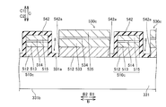
- the red semiconductor laser device 10 includes an n-type contact layer 12 made of Si-doped GaAs, an n-type cladding layer 13 made of Si-doped AlGaInP, on the upper surface of an n-type GaAs substrate 11.
- MQW multiple quantum well
- the p-type cladding layer 15 has a convex portion extending in a stripe shape along the laser light emission direction, and a flat portion extending on both sides (B direction) of the convex portion.
- a ridge 20 for forming an optical waveguide is formed by the convex portion of the p-type cladding layer 15.
- the “laser light emitting portion” of the present invention is formed in the portion of the active layer 14 below the ridge 20.
- a current blocking layer 16 made of SiO 2 is formed so as to cover the upper surface of the p-type cladding layer 15 other than the ridge 20.
- a p-side pad electrode 17 made of Au or the like is formed so as to cover the top surfaces of the ridge 20 and the current blocking layer 16.
- a contact layer or an ohmic electrode layer having a smaller band gap than the p-type cladding layer 15 may be formed between the ridge 20 and the p-side pad electrode 17.
- an n-side electrode 18 in which a Ti layer, a Pt layer, and an Au layer are stacked in this order from the n-type GaAs substrate 11 side is formed on the lower surface (the C1 side surface) of the n-type GaAs substrate 11.
- the green semiconductor laser device 30 includes an n-type GaN layer 32 made of Ge-doped GaN and an n-type cladding layer 33 made of Si-doped n-type AlGaN on the upper surface of an n-type GaN substrate 31. And an active layer 34 having an MQW structure in which quantum well layers and barrier layers made of InGaN are alternately stacked, and a p-type cladding layer 35 made of Mg-doped p-type AlGaN.
- the p-type cladding layer 35 has a convex portion extending in a stripe shape along the laser beam emission direction, and a flat portion extending on both sides (B direction) of the convex portion.
- a ridge 40 for forming an optical waveguide is formed by the convex portion of the p-type cladding layer 35.
- the “laser emitting portion” of the present invention is formed in the portion of the active layer 34 below the ridge 40.
- a current blocking layer 36 made of SiO 2 is formed so as to cover the upper surface of the p-type cladding layer 35 other than the ridge 40.
- a p-side pad electrode 37 made of Au or the like is formed so as to cover the upper surfaces of the ridge 40 and the current blocking layer 36.
- a contact layer, an ohmic electrode layer, or the like preferably having a smaller band gap than the p-type cladding layer 35 may be formed between the ridge 40 and the p-side pad electrode 37.
- an n-side electrode 38 is formed in which a Ti layer, a Pt layer, and an Au layer are stacked in this order from the n-type GaN substrate 31 side.
- the blue semiconductor laser device 50 includes an n-type GaN layer 52 made of Ge-doped GaN and an n-type clad layer 53 made of Si-doped n-type AlGaN on the upper surface of an n-type GaN substrate 51. Then, an active layer 54 having an MQW structure in which quantum well layers and barrier layers made of InGaN are alternately stacked, and a p-type cladding layer 55 made of Mg-doped p-type AlGaN are formed.
- the p-type cladding layer 55 has a convex portion extending in a stripe shape along the laser light emission direction, and a flat portion extending on both sides (B direction) of the convex portion.
- a ridge 60 for forming an optical waveguide is formed by the convex portion of the p-type cladding layer 55.
- the “laser light emitting portion” of the present invention is formed in the portion of the active layer 54 below the ridge 60.
- a current blocking layer 56 made of SiO 2 is formed so as to cover the upper surface of the p-type cladding layer 55 other than the ridge 60.
- a p-side pad electrode 57 made of an Au layer or the like is formed so as to cover the top surfaces of the ridge 60 and the current blocking layer 56.
- a contact layer or an ohmic electrode layer having a smaller band gap than that of the p-type cladding layer 55 may be formed.
- an n-side electrode 58 is formed in which a Ti layer, a Pt layer, and an Au layer are stacked in this order from the n-type GaN substrate 51 side.
- the semiconductor laser device 100 includes a pedestal 110 on which the RGB three-wavelength semiconductor laser element unit 90 is placed, and five lead terminals 101 that are electrically insulated from the pedestal 110 and penetrate the bottom 107a. , 102, 103, 104 and 105, and a stem 107 provided with a lead terminal 106 (shown by a broken line) which is electrically connected to the base 110 and the bottom 107a.
- the three red semiconductor laser elements 10 are connected to the lead terminals 101, 102, and 105 through metal wires 71, 72, and 73 that are wire-bonded to the p-side pad electrodes 17, respectively.
- the p-side pad electrode 17 is an example of the “electrode” in the present invention
- each of the lead terminals 101, 102, and 105 is an example of the “terminal” in the present invention.
- the two green semiconductor laser elements 30 are commonly connected to one lead terminal 103 via metal wires 74 and 75 wire-bonded to the respective p-side pad electrodes 37 (see FIG. 2). Further, the blue semiconductor laser element 50 is connected to the lead terminal 104 via a metal wire 76 wire-bonded to the p-side pad electrode 57 (see FIG. 2).
- the base 91 on which the semiconductor laser elements (10, 30 and 50) are placed is made of a conductive material such as AlN, and is electrically connected to the pedestal 110 via the conductive adhesive layer 1. Yes.
- the semiconductor laser device 100 includes lead terminals (101, 102, 103, 104 and 105) in which the p-side electrodes (17, 37 and 57) of the semiconductor laser elements (10, 30 and 50) are insulated from each other. And the n-side electrode (18, 38 and 58) is connected to a common negative terminal (lead terminal 106 (see FIG. 1)) (cathode common).
- the red semiconductor laser element 10, the green semiconductor laser element 30, and the blue semiconductor laser element 50 have a light emitting surface and a light reflecting surface at both ends in the cavity direction (direction perpendicular to the paper surface of FIG. 1). Is formed.
- a low-reflectivity dielectric multilayer film is formed on the light emission surface of each semiconductor laser element (the surface on the emission direction side of each color laser beam), and the light reflection surface (emission of laser light of each color).
- a dielectric multilayer film having a high reflectivity is formed on the surface opposite to the direction).
- the dielectric multilayer film GaN, AlN, BN, Al 2 O 3 , SiO 2 , ZrO 2 , Ta 2 O 5 , Nb 2 O 5 , La 2 O 3 , SiN, AlON and MgF 2 ,
- a multilayer film made of Ti 3 O 5 , Nb 2 O 3, or the like which is a material having a different hybrid ratio can be used.
- a light guide layer, a carrier block layer, or the like may be formed between the n-type cladding layer and the active layer. Further, a contact layer or the like may be formed on the opposite side of the n-type cladding layer from the active layer. Further, a light guide layer, a carrier block layer, or the like may be formed between the active layer and the p-type cladding layer. Further, a contact layer or the like may be formed on the opposite side of the p-type cladding layer from the active layer.
- the active layer may be a single layer or a single quantum well (SQW) structure.
- the n-type contact layer 12 and the n-type cladding layer 13 are formed on the upper surface of the n-type GaAs substrate 11 by using the MOCVD method. Then, the active layer 14 and the p-type cladding layer 15 are sequentially formed, and then the ridge 20, the current blocking layer 16, and the p-side pad electrode 17 are formed. Thereafter, the lower surface of the n-type GaAs substrate 11 is polished, and then an n-side electrode 18 is formed on the lower surface of the n-type GaAs substrate 11 to produce a wafer of the red semiconductor laser device 10.
- the wafer is cleaved in a bar shape so as to have a predetermined resonator length, and a plurality of red semiconductor laser elements 10 (see FIG. 1) are formed by dividing the elements in the resonator direction into chips.
- the green semiconductor laser element 30 and the blue semiconductor laser element 50 are formed by the same manufacturing process as that of the red semiconductor laser element 10.
- three red semiconductor laser elements 10, two green semiconductor laser elements 30, and one blue semiconductor laser element 50 are used using a ceramic collet (not shown). Are fixed via the conductive adhesive layer 2 while being pressed against the base 91.
- the semiconductor laser elements of the respective colors have the laser beams of the respective colors substantially parallel to each other and viewed from the laser beam emission direction side from one side end (B1 side) to the other side end (B2 side). Toward, they are arranged in the order of red, green, red, blue, red, and green. In this way, the RGB three-wavelength semiconductor laser element unit 90 is formed.
- the conductive adhesive layer 1 is pressed while pressing the RGB three-wavelength semiconductor laser element portion 90 against the pedestal 110 provided on the stem 107 so that the emission directions of the laser beams of the respective colors are directed to the front direction of the bottom portion 107 a of the stem 107. Join through.
- the base 91 is electrically connected to the lead terminal 106 via the base 110.
- the p-side pad electrode 17 of each red semiconductor laser element 10 and the lead terminals 101, 102, and 105 are connected by metal wires 71, 72, and 73, respectively.
- the p-side pad electrode 37 and the lead terminal 103 of each of the green semiconductor laser elements 30 are connected by metal wires 74 and 75, respectively.
- the p-side pad electrode 57 of the blue semiconductor laser element 50 and the lead terminal 104 are connected by a metal wire 76. In this way, the semiconductor laser device 100 according to the first embodiment is formed.
- the configuration of the projector device 150 which is an example of the “display device” of the present invention, on which the semiconductor laser device 100 according to the first embodiment of the present invention is mounted will be described.
- the projector device 150 an example in which individual semiconductor laser elements constituting the semiconductor laser device 100 are turned on substantially simultaneously will be described.
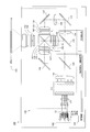
- the projector device 150 includes a semiconductor laser device 100, an optical system 120 including a plurality of optical components, and a control unit 145 that controls the semiconductor laser device 100 and the optical system 120.
- the laser light emitted from the semiconductor laser device 100 is modulated by the optical system 120 and then projected onto the external screen 144 or the like.
- the optical system 120 is an example of the “modulation means” in the present invention.
- the laser light emitted from the semiconductor laser device 100 is converted into parallel light having a predetermined beam diameter by the dispersion angle control lens 122 composed of a concave lens and a convex lens, and then incident on the fly eye integrator 123.
- the fly-eye integrator 123 is configured so that two fly-eye lenses made up of eyelet-shaped lens groups face each other, so that the light quantity distribution when entering the liquid crystal panels 129, 133 and 140 is uniform.
- the lens action is given to the light incident from the dispersion angle control lens 122. That is, the light transmitted through the fly-eye integrator 123 is adjusted so as to be incident with a spread of an aspect ratio (for example, 16: 9) corresponding to the size of the liquid crystal panels 129, 133, and 140.
- the light transmitted through the fly eye integrator 123 is collected by the condenser lens 124.
- the condenser lens 124 Of the light transmitted through the condenser lens 124, only red light is reflected by the dichroic mirror 125, while green light and blue light are transmitted through the dichroic mirror 125.
- the red light is incident on the liquid crystal panel 129 via the incident side polarizing plate 128 after being collimated by the lens 127 through the mirror 126.
- the liquid crystal panel 129 modulates red light by being driven in accordance with a red drive signal (R image signal).
- dichroic mirror 130 only green light out of the light transmitted through the dichroic mirror 125 is reflected, while blue light passes through the dichroic mirror 130.
- the green light is incident on the liquid crystal panel 133 through the incident-side polarizing plate 132 after being collimated by the lens 131.
- the liquid crystal panel 133 modulates green light by being driven according to a green driving signal (G image signal).
- the blue light transmitted through the dichroic mirror 130 passes through the lens 134, the mirror 135, the lens 136, and the mirror 137, is further collimated by the lens 138, and then enters the liquid crystal panel 140 through the incident-side polarizing plate 139. Is done.
- the liquid crystal panel 140 modulates blue light by being driven according to a blue driving signal (B image signal).
- the red light, the green light, and the blue light modulated by the liquid crystal panels 129, 133, and 140 are combined by the dichroic prism 141 and then incident on the projection lens 143 through the output side polarizing plate 142.
- the projection lens 143 adjusts the zoom and focus of the projected image by displacing a lens group for forming an image of projection light on the projection surface (screen 144) and a part of the lens group in the optical axis direction. Built-in actuator for.
- the control unit 145 causes the steady voltage as the R signal related to the driving of the red semiconductor laser element 10, the G signal related to the driving of the green semiconductor laser element 30, and the B signal related to the driving of the blue semiconductor laser element 50.
- the semiconductor laser device 100 is controlled to be supplied to each laser element.
- the red semiconductor laser element 10, the green semiconductor laser element 30, and the blue semiconductor laser element 50 of the semiconductor laser device 100 are configured to oscillate substantially simultaneously.
- the control unit 145 controls the light intensity of each of the red semiconductor laser element 10, the green semiconductor laser element 30, and the blue semiconductor laser element 50 of the semiconductor laser device 100, so that the hue of the pixels projected on the screen 144 The brightness and the like are controlled. Accordingly, a desired image is projected on the screen 144 by the control unit 145. In this way, the projector device 150 on which the semiconductor laser device 100 according to the first embodiment of the present invention is mounted is configured.
- FIG. 1, FIG. 4, and FIG. 5 the configuration of a projector device 190, which is another example of the “display device” of the present invention, on which the semiconductor laser device 100 according to the first embodiment of the present invention is mounted. Will be described.
- the projector apparatus 190 an example in which individual semiconductor laser elements constituting the semiconductor laser apparatus 100 are turned on in time series will be described.
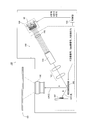
- the projector device 190 includes the semiconductor laser device 100, the optical system 160, and a control unit 185 that controls the semiconductor laser device 100 and the optical system 160.
- the laser light from the semiconductor laser device 100 is modulated by the optical system 160 and then projected onto the screen 181 or the like.
- the optical system 160 is an example of the “modulation means” in the present invention.
- the laser light emitted from the semiconductor laser device 100 is converted into parallel light by the lens 162, and then enters the light pipe 164.
- the inner surface of the light pipe 164 is a mirror surface, and the laser light travels through the light pipe 164 while being repeatedly reflected by the inner surface of the light pipe 164. At this time, the intensity distribution of the laser light of each color emitted from the light pipe 164 is made uniform by the multiple reflection action in the light pipe 164.
- the laser light emitted from the light pipe 164 is incident on the digital micromirror device (DMD) element 166 via the relay optical system 165.
- DMD digital micromirror device
- the DMD element 166 is composed of a group of minute mirrors arranged in a matrix. Further, the DMD element 166 expresses the gradation of each pixel by switching the light reflection direction at each pixel position between a first direction A toward the projection lens 180 and a second direction B deviating from the projection lens 180. (Modulation) function. Of the laser light incident on each pixel position, the light (ON light) reflected in the first direction A is incident on the projection lens 180 and projected onto the projection surface (screen 181). The light (OFF light) reflected in the second direction B by the DMD element 166 is absorbed by the light absorber 167 without entering the projection lens 180.
- the control unit 185 controls the pulse power to be supplied to the semiconductor laser device 100, whereby the red semiconductor laser element 10, the green semiconductor laser device 30, and the blue semiconductor laser of the semiconductor laser device 100 are controlled.
- the element 50 is configured to be divided in time series and periodically driven one element at a time.
- the control unit 185 causes the DMD element 166 of the optical system 160 to synchronize with the driving states of the red semiconductor laser element 10, the green semiconductor laser element 30, and the blue semiconductor laser element 50, respectively. ) To modulate the light in accordance with the gradation.
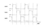
- an R signal related to driving of the red semiconductor laser element 10 (see FIG. 1)
- a G signal related to driving of the green semiconductor laser element 30 (see FIG. 1)
- a blue semiconductor laser element 50 The B signal related to the driving (see FIG. 1) is supplied to each laser element of the semiconductor laser device 100 by the control unit 185 (see FIG. 4) in a state of being divided in time series so as not to overlap each other.
- the control unit 185 outputs the B image signal, the G image signal, and the R image signal to the DMD element 166, respectively.
- the blue light of the blue semiconductor laser element 50 is emitted based on the B signal in the timing chart shown in FIG. 5, and the blue light is modulated by the DMD element 166 based on the B image signal at this timing. Is done. Further, green light from the green semiconductor laser element 30 is emitted based on the G signal output next to the B signal, and at this timing, the green light is modulated by the DMD element 166 based on the G image signal. The Further, red light from the red semiconductor laser element 10 is emitted based on the R signal output next to the G signal, and at this timing, the red light is modulated by the DMD element 166 based on the R image signal.
- the blue light of the blue semiconductor laser element 50 is emitted based on the B signal output next to the R signal.
- the blue light is again emitted from the DMD element 166 based on the B image signal. Modulated.
- an image by laser light irradiation based on the B image signal, the G image signal, and the R image signal is projected onto the projection surface (screen 181).
- the projector device 190 on which the semiconductor laser device 100 according to the first embodiment of the present invention is mounted is configured.
- the number n1 (three) of the red semiconductor laser elements 10 is larger than the number n2 (two) of the green semiconductor laser elements 30, and the green semiconductor
- the number n2 (two) of the laser elements 30 is configured to be larger than the number n3 (one) of the blue semiconductor laser elements 50
- the base 91 on the base 91, three red semiconductor laser elements 10 having a rated output of about 800 mW, two green semiconductor laser elements 30 having a rated output of about 400 mW, and blue having a rated output of about 700 mW.
- the formed semiconductor laser device 100 can be easily formed.
- each p-side pad electrode 17 is connected to different lead terminals 101, 102, and 105 via metal wires 71, 72, and 73, respectively.
- the red semiconductor laser elements 10 having more laser light emitting parts than the green semiconductor laser elements 30 and the blue semiconductor laser elements 50 can be individually driven according to the number of laser light emitting parts. Accordingly, the total output of the red semiconductor laser element 10 can be easily adjusted.
- the second embodiment will be described with reference to FIGS.
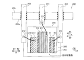
- a monolithic red semiconductor laser element unit 210 in which four red semiconductor laser elements 210a to 210d are integrated, and two green semiconductor laser elements 230a and 230b are provided.
- an RGB monochromatic semiconductor laser element unit 290 is configured by disposing an integrated monolithic green semiconductor laser element unit 230 and one blue semiconductor laser element 50 on a base 291.
- the RGB three-wavelength semiconductor laser element portion 290 is fixed on the upper surface (surface on the C2 side) of the pedestal 206.
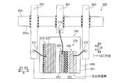
- the monolithic red semiconductor laser element unit 210 includes four red semiconductor laser elements 210a to 210d having a rated oscillation of 700 mW and an oscillation wavelength of about 655 nm. It is configured to be integrated on the substrate 211 and to have a total output of about 2.8W.
- the monolithic green semiconductor laser element section 230 has two green semiconductor laser elements 230a and 230b having a rated 400 mW and an oscillation wavelength of about 530 nm integrated on a single substrate 231. And a total output of about 800 mW.
- the red semiconductor laser element portion 210, the green semiconductor laser element portion 230, and one blue semiconductor laser element 50 having an output of about 700 mW are connected to the upper surface (on the C2 side) of the base 291. Surface) at a predetermined interval.
- each of the semiconductor laser elements constituting the red semiconductor laser element unit 210 and the green semiconductor laser element unit 230 When comparing the number of laser light emitting portions of the red semiconductor laser elements 210a to 210d that emit relatively long wavelengths, the four laser light emitting portions of the green semiconductor laser elements 230a that emit relatively short wavelengths More than the two laser light emitting portions 230b are formed.
- the green semiconductor laser element 230a that emits a relatively long wavelength.
- the laser light emitting portions (two) of 230b and 230b are formed more than the laser light emitting portions (one) of the blue semiconductor laser element 50 emitting a relatively short wavelength. In this way, white light is obtained from the RGB three-wavelength semiconductor laser element portion 290.
- the laser beam emission direction (A1 direction) is orthogonal to the B direction at the approximate center in the width direction (B direction) of the semiconductor laser device 200 on the base 291.
- the red semiconductor laser element portion 210 is disposed so as to be adjacent to the red semiconductor laser element portion 210 on one side end side (B1 direction side) on the base 291 and the emission direction of the laser light is red.
- the green semiconductor laser element portion 230 is arranged so as to be substantially parallel to the emission direction (A1 direction) of the laser light from the semiconductor laser element portion 210.
- the blue semiconductor laser element 50 is adjacent to the red semiconductor laser element part 210 on the opposite side (B2 direction) from the green semiconductor laser element part 230, and the laser beam is emitted from the red semiconductor laser element part 210. It arrange
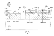
- the red semiconductor laser elements 210a to 210d are integrally formed on the substrate 211 with the recess 5 therebetween.
- a p-side pad electrode 217 that is used in common over the red semiconductor laser elements 210a to 210d is formed on the surface of the red semiconductor laser elements 210a to 210d on the p-type cladding layer 15 side (C2 side).
- An n-side electrode 218 is formed on the lower surface (C1 side) of the substrate 211.
- the green semiconductor laser elements 230a and 230b are integrally formed on the substrate 231 with a recess 6 reaching the n-type GaN layer 32 from the upper surface (surface on the C2 side) of the green semiconductor laser element portion 230. Is formed.
- the current blocking layer 36 is formed so as to cover the side surface and the bottom surface of the recess 6.
- a p-side pad electrode 237 used in common with the green semiconductor laser elements 230a and 230b is formed on the surface of the green semiconductor laser elements 230a and 230b on the p-type cladding layer 35 side (C2 side).
- An n-side electrode 238 is formed on the lower surface (C1 side) of the substrate 231.
- the other configuration of the green semiconductor laser element unit 230 is the same as that of the green semiconductor laser element 30 of the first embodiment.
- the semiconductor laser device 200 includes a pedestal 206 on which the RGB three-wavelength semiconductor laser element unit 290 is mounted, and three lead terminals 201 that are electrically insulated from the pedestal 206 and penetrate the bottom 205a. , 202 and 203, and a stem 205 provided with a pedestal 206 and another lead terminal (not shown) that is electrically connected to the base 205a.
- the red semiconductor laser element portion 210 is connected to the lead terminal 201 via a metal wire 271 wire-bonded to the p-side pad electrode 217.
- the green semiconductor laser element section 230 is connected to the lead terminal 202 via a metal wire 272 wire-bonded to the p-side pad electrode 237.
- the blue semiconductor laser element 50 is connected to the lead terminal 203 through a metal wire 273 wire-bonded to the p-side pad electrode 57.
- the red semiconductor laser element part 210, the green semiconductor laser element part 230, and the blue semiconductor laser element 50 are formed on the upper surface (surface on the C2 side) of the base 291 through a conductive adhesive layer (not shown) such as AuSn solder.
- the base 291 is electrically connected to the base 206 via a conductive adhesive layer (not shown) such as AuSn solder.
- a conductive adhesive layer such as AuSn solder.
- the laser beam of each color may be radiate
- the four red semiconductor laser elements 210a to 210d are formed on the common substrate 211 to form the monolithic red semiconductor laser element unit 210, and the two green semiconductor laser elements 230a and 230b are formed on a common substrate 231 to form a monolithic green semiconductor laser element portion 230, whereby the red semiconductor laser element portion 210 and the green semiconductor laser element portion 230 are common to each oscillation wavelength. Since they are integrated on the substrate, the width in the B direction of the red semiconductor laser element portion 210 and the green semiconductor laser element portion 230 can be reduced by the amount of integration.
- the red semiconductor laser element part 210 can be easily placed in the package (on the base 291).
- the remaining effects of the second embodiment are similar to those of the aforementioned first embodiment.
- a third embodiment will be described with reference to FIG. 6 and FIGS.
- a monolithic type 2 in which a green semiconductor laser element portion 330 including two green semiconductor laser elements 330a and 330b and one blue semiconductor laser element 350 are integrated.
- the case where the wavelength semiconductor laser element unit 370 and the red semiconductor laser element unit 210 are arranged on the base 391 to constitute the RGB three wavelength semiconductor laser element unit 390 will be described.
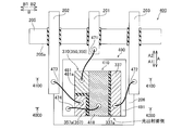
- the RGB three-wavelength semiconductor laser element portion 390 is fixed on the upper surface of the pedestal 206 as shown in FIG.
- the RGB three-wavelength semiconductor laser element unit 390 includes a red semiconductor laser element unit 210, two green semiconductor laser elements 330a and 330b, and one blue semiconductor laser.
- a monolithic two-wavelength semiconductor laser element portion 370 in which the element 350 is integrated on one n-type GaN substrate 331 is connected to a base 391 via a conductive adhesive layer (not shown) such as AuSn solder. It is fixed on the top surface.
- the two-wavelength semiconductor laser element unit 370 is formed by integrating a green semiconductor laser element unit 330 and a blue semiconductor laser element 350 on a common n-type GaN substrate 331 having a (11-22) principal surface. Is formed.
- the n-type GaN substrate 331 is an example of the “substrate” in the present invention.
- the (11-22) plane of the n-type GaN substrate 331 is about 58 ° from the c plane ((0001) plane) toward the [11-20] direction. It is composed of a semipolar surface composed of inclined surfaces. As the semipolar plane, it is preferable to use a plane inclined by about 10 ° or more and about 70 ° or less from the c-plane. As a result, the green semiconductor laser element portion 330 and the blue semiconductor laser element 350 can substantially match the extending direction of the optical waveguide in which the optical gain is maximized.
- the (11-22) plane has a smaller piezoelectric field than other semipolar planes, it is possible to suppress a decrease in the light emission efficiency of the blue semiconductor laser element 350 and the green semiconductor laser element section 330. It is. Therefore, it is more preferable to use the above-described (11-22) plane as the main surface of the n-type GaN substrate 331.
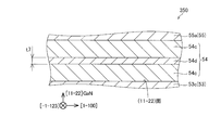
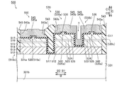
- the blue semiconductor laser element 350 includes an n-type GaN layer 52 and a Si-doped n-type Al layer having a thickness of about 2 ⁇ m in a region on the [ ⁇ 1100] direction (B1 direction) side on the upper surface of the n-type GaN substrate 331.
- an n-type light guide layer 53c made of Si-doped n-type In 0.02 Ga 0.98 N is formed.
- the active layer 54 in the blue semiconductor laser element 350 has the same main surface as the (11-22) plane as the n-type GaN substrate 331.
- the active layer 54 is a four-layer barrier made of undoped In 0.02 Ga 0.98 N having a thickness of about 20 nm on the upper surface of the n-type light guide layer 53c.
- the layers 54a and three well layers 54b made of undoped In 0.20 Ga 0.80 N having a thickness t5 of about 3 nm are alternately stacked.
- the in-plane lattice constant of the well layer 54b is larger than the in-plane lattice constant of the n-type GaN substrate 331, compressive strain is applied in the in-plane direction.
- the well layer 54b is an example of the “first well layer” in the present invention. That is, the well layer 54b of the active layer 54 of the blue semiconductor laser element 350 has an In composition of about 20%.
- the (11-22) plane is used as the main surface of the active layer 54 as compared with the case where the polar c-plane ((0001) plane) and other semipolar surfaces are applied to the main surface of the active layer 54. As a result, the piezoelectric field in the active layer 54 can be reduced.
- the polarization direction that maximizes the oscillator strength within the main surface of the blue semiconductor laser element 350 is a direction perpendicular to the m-plane ((1-100) plane) that is a nonpolar plane [1-100. ] Direction.
- the blue semiconductor laser element 350 includes a p-type light guide layer made of Mg-doped p-type In 0.02 Ga 0.98 N having a thickness of about 100 nm on the upper surface of the active layer 54.
- 55a a p-type carrier block layer 55b made of Mg-doped p-type Al 0.16 Ga 0.84 N having a thickness of about 20 nm, and an Mg-doped p-type Al 0.07 Ga 0.93 having a thickness of about 700 nm.
- a stripe-shaped ridge 360 is formed at a substantially central portion in the B direction (B1 direction and B2 direction) of the blue semiconductor laser element 350 by the p-type cladding layer 55c and the p-type contact layer 55d.
- the ridge 360 is formed so as to extend along the direction ([ ⁇ 1-123] direction) in which the optical waveguide extends, which is the direction in which the [0001] direction is projected onto the (11-22) plane.
- a current blocking layer 376 made of an insulating film is formed so as to cover the side surface of 55c and expose the upper surface of the ridge 360.
- the current blocking layer 376 is made of SiO 2 and has a thickness of about 250 nm.
- the current blocking layer 376 includes a predetermined region on the upper surface of the n-type GaN substrate 331 (a region exposed from the blue semiconductor laser element 350 and the green semiconductor laser element unit 330) and a p-type described later of the green semiconductor laser element unit 330.
- the upper surface of the ridge 340 covers the upper surface of the flat portion of the clad layer 35c, the side surfaces of the ridge 340, which will be described later, and the side surfaces of the n-type semiconductor layer (33), the active layer 34, and the p-type semiconductor layer (35). Is formed to be exposed.
- the current blocking layer 376 is formed so as to cover the side surface and the bottom surface of the recess 7.
- the p-side ohmic electrode 56 is formed.
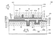
- the green semiconductor laser element portion 330 is formed on the upper surface of the n-type GaN substrate 331 with the concave portion 8 on the side opposite to the blue semiconductor laser element 350 (B2 side). Further, as shown in FIG. 10, the green semiconductor laser elements 330a and 330b arranged side by side in the direction (B direction) in which the laser elements are arranged across the recess 7 in the green semiconductor laser element section 330 are blue semiconductor laser elements.
- the n-type GaN layer 32 having a thickness of about 1 ⁇ m and a thickness of about 2 ⁇ m
- An n-type cladding layer 33a made of Si-doped n-type Al 0.10 Ga 0.90 N
- an n-type carrier block layer 33b made of Si-doped n-type Al 0.20 Ga 0.80 N having a thickness of about 5 nm
- an n-type light guide layer 33c made of Si-doped n-type In 0.05 Ga 0.95 N having a thickness of about 100 nm.
- the active layer 34 in the green semiconductor laser element section 330 has the same main surface as the (11-22) plane as the n-type GaN substrate 331.
- the active layer 34 is a two-layer barrier made of undoped In 0.02 Ga 0.98 N having a thickness of about 20 nm on the upper surface of the n-type light guide layer 33c. It has an SQW structure in which layers 34a and one well layer 34b made of undoped In 0.33 Ga 0.67 N having a thickness t6 of about 3.5 nm are alternately stacked.
- the thickness t6 of the well layer 34b is preferably less than about 6 nm.
- the active layer 34b of the active layer 34 has an SQW structure as compared to the case where the active layer 34 has an MQW structure, so that the well layer 34b has a layer structure. It is possible to maintain.
- the well layer 34b is an example of the “second well layer” in the present invention. That is, the well layer 34b of the active layer 34 of the green semiconductor laser element section 330 has an In composition of about 33%, which is larger than the In composition (about 20%) of the well layer 54b of the active layer 54 of the blue semiconductor laser element 350. is doing.
- the extending direction of the optical waveguide (ridge 340) in which the gain of the green semiconductor laser elements 330a and 330b is maximized and the extending direction of the optical waveguide (ridge 360) in which the gain of the blue semiconductor laser element 350 is maximized. are in the same direction ([ ⁇ 1-123] direction).
- the extending direction of the optical waveguide (ridge 340) in which the gain of the green semiconductor laser elements 330a and 330b is maximized and the extending direction of the optical waveguide (ridge 360) in which the gain of the blue semiconductor laser element 350 is maximized. are in the same direction ([ ⁇ 1-123] direction) when the In composition is about 30% or more, the thickness of the well layer made of InGaN having the (11-22) principal surface is about 3 nm. If less than this, it is based on the finding that the main polarization direction in the (11-22) plane is rotated by 90 ° (from [1-100] direction) to [ ⁇ 1-123] direction). .
- the thickness t6 of the well layer 34b is more preferably about 3 nm or more.
- the well layer 34b made of InGaN having an In composition of about 33% and having a main surface of (11-22) plane has a thickness t6 of about 3.5 nm (about 3 nm or more).
- the in-plane lattice constant of the well layer 34b is larger than the in-plane lattice constant of the n-type GaN substrate 331 (see FIG. 10), compressive strain is applied in the in-plane direction. Further, the compressive strain of the well layer 34 b of the green semiconductor laser element portion 330 is larger than the compressive strain of the well layer 54 b of the blue semiconductor laser element 350. Also, the (11-22) plane is the main surface of the active layer 34 as compared with the case where the c-plane ((0001) plane), which is a polar surface, and other semipolar surfaces are the main surfaces of the active layer 34. Thus, the piezoelectric field in the active layer 34 can be reduced.
- the thickness t6 (about 3.5 nm) of the well layer 34b of the active layer 34 of the green semiconductor laser elements 330a and 330b shown in FIG. 12 is the same as that of the well layer 54b of the active layer 54 of the blue semiconductor laser element 350 shown in FIG.
- Each layer is configured to be larger than the thickness t5 (about 3 nm) (t6> t5).
- the green semiconductor laser elements 330a and 330b are p-type light composed of Mg-doped p-type In 0.05 Ga 0.95 N having a thickness of about 100 nm on the upper surface of the active layer 34.
- a p-type cladding layer 35c made of .90 N and a p-type contact layer 35d made of Mg-doped p-type In 0.02 Ga 0.98 N having a thickness of about 10 nm are formed.
- the p-type cladding layer 35c and the p-type contact layer 35d form a striped ridge 340 at substantially the center in the B direction (B1 direction and B2 direction) of each of the green semiconductor laser elements 330a and 330b.
- the ridge 340 is formed to extend along the direction ([ ⁇ 1-123] direction) in which the optical waveguide extends, which is the direction in which the [0001] direction is projected onto the (11-22) plane.
- the Al composition (about 10%) of the n-type cladding layer 33a and the p-type cladding layer 35c of the green semiconductor laser devices 330a and 330b is the Al composition of the n-type cladding layer 53a and the p-type cladding layer 55c of the blue semiconductor laser device 350. It is configured to be larger than the composition (about 7%). Further, the Al composition (about 20%) of the n-type carrier block layer 33b and the p-type carrier block layer 35b of the green semiconductor laser elements 330a and 330b is the same as that of the n-type carrier block layer 53b and the p-type carrier block of the blue semiconductor laser element 350. The layer 55b is configured to be larger than the Al composition (about 16%).
- the In composition (about 5%) of the n-type light guide layer 33c and the p-type light guide layer 35a of the green semiconductor laser elements 330a and 330b is the same as the n-type light guide layer 53c and the p-type light guide of the blue semiconductor laser element 350.
- the layer 55a is configured to be larger than the In composition (about 2%).
- the Al compositions of the n-type cladding layer 33a, the n-type carrier block layer 33b, the p-type carrier block layer 35b, and the p-type cladding layer 35c of the green semiconductor laser elements 330a and 330b are respectively n of the blue semiconductor laser element 350. It is preferable that it is larger than the Al composition of the type cladding layer 53a, n-type carrier block layer 53b, p-type carrier block layer 55b and p-type cladding layer 55c.
- the light confinement function is lowered, but the lattice constants of the crystal lattices of the AlGaN and the n-type GaN substrate 331 are different. It is possible to reduce the occurrence of cracks and warpage due to the above.
- the In composition of the n-type light guide layer 33c and the p-type light guide layer 35a of the green semiconductor laser elements 330a and 330b is the same as that of the n-type light guide layer 53c and the p-type light guide layer 55a of the blue semiconductor laser element 350. The larger one is preferable.
- a p-side ohmic electrode 36 made of the same material as the p-side ohmic electrode 56 of the blue semiconductor laser element 350 is formed on the upper surface of the p-type contact layer 35d.
- the two-wavelength semiconductor laser element portion 370 is a recess that reaches the n-type GaN layer 32 from the upper surface (the C2 side surface) of the two-wavelength semiconductor laser element portion 370 on the n-type GaN substrate 331.
- Two green semiconductor laser elements 330a and 330b are formed with a distance 7 therebetween, and adjacent to the green semiconductor laser element 330a side with a recess 8 reaching the n-type GaN substrate 331 from the upper surface of the two-wavelength semiconductor laser element section 370.
- one blue semiconductor laser element 350 is formed.
- a layer 376 is formed.
- the current blocking layer 376 is formed so as to cover the inner surface and the bottom surface of the recess 8, the both side surfaces of the ridge 360 of the blue semiconductor laser element 350, and the flat portion of the p-type cladding layer 55c.
- a p-side pad electrode 337 in which a Ti layer having a thickness of 100 nm, a Pd layer having a thickness of about 100 nm, and an Au layer having a thickness of about 3 ⁇ m are stacked is formed, and the current of the blue semiconductor laser element 350 is
- a p-side pad electrode 357 having the same structure as the p-side pad electrode 337 and electrically connected to the p-side ohmic electrode 56 is formed on the block layer 376.
- the blue semiconductor laser element 350 and the green semiconductor laser elements 330a and 330b have resonator planes perpendicular to the extending direction of the optical waveguide ([-123] direction), respectively. Is formed. That is, the blue semiconductor laser element 350 and the green semiconductor laser elements 330a and 330b are configured to have resonator surfaces having the same plane orientation.
- the other configurations of the green semiconductor laser elements 330a and 330b and the blue semiconductor laser element 350 constituting the two-wavelength semiconductor laser element unit 370 are respectively the green semiconductor of the green semiconductor laser element unit 230 in the second embodiment. This is the same as the laser elements 230a and 230b.
- a red semiconductor laser element portion 210 is disposed on the B1 direction side on the base 391, and a two-wavelength semiconductor laser element portion 370 is disposed on the B2 direction side.
- the red semiconductor laser element part 210 is connected to the lead terminal 202 through a metal wire 371 wire-bonded to the p-side pad electrode 217.
- the green semiconductor laser element portion 330 of the two-wavelength semiconductor laser element portion 370 is connected to the lead terminal 203 via a metal wire 372 that is wire-bonded to the p-side pad electrode 337.
- the blue semiconductor laser element 350 is connected to the lead terminal 201 through a metal wire 373 wire-bonded to the p-side pad electrode 357.
- the remaining structure of the semiconductor laser device 300 according to the third embodiment is similar to that of the aforementioned second embodiment.
- the blue color is formed on the upper surface of the n-type GaN substrate 331 having the main surface consisting of (11-22) plane by MOCVD.
- a p-type cladding layer 55c is sequentially formed.
- n-type GaN layer 32, the n-type cladding layer 33a, the n-type carrier block layer 33b, the n-type light guide layer 33c, the active layer 34, and the p-type light guide layers 35a, p which leave the region and become the green semiconductor laser element portion 330
- a type carrier block layer 35b and a p-type cladding layer 35c are sequentially formed.
- a recess 7 whose bottom surface reaches the n-type GaN layer 32 is formed.
- p-type contact layers 35d and 55d and p Side ohmic electrodes 36 and 56 are formed.
- a current blocking layer 376 is formed so as to cover the surface of the p-type cladding layer 35c (55c) and the side surfaces and the bottom surface of each of the recess 7 and the recess 8.
- p-side pad electrodes 337 and 357 are formed for the respective laser elements so as to cover a predetermined region of current blocking layer 376 and p-side ohmic electrodes 36 and 56.
- the p-side pad electrode 337 is formed on the side surface and the bottom surface of the recess 7 and used in common for the green semiconductor laser elements 330a and 330b.
- the green semiconductor laser element portion 330 is formed on the surface of the same n-type GaN substrate 331 as the n-type GaN substrate 331 on which the blue semiconductor laser element 350 is formed. Therefore, it is possible to prevent the active layer 34 of the green semiconductor laser element portion 330, which is easily deteriorated by heat due to a large In composition, from being affected by heat when the blue semiconductor laser element 350 is formed. In this manner, the blue semiconductor laser element 350 and the green semiconductor laser element part 330 are manufactured, which are separated at a predetermined interval in the B direction by the recesses 8 whose bottoms reach the n-type GaN substrate 331.
- the lower surface of the n-type GaN substrate 331 is polished to a thickness of about 100 ⁇ m, and then an n-side electrode 378 is formed on the lower surface of the n-type GaN substrate 331 to produce a wafer of the two-wavelength semiconductor laser element portion 370. .
- a resonator plane perpendicular to the extending direction of the optical waveguide ([ ⁇ 1-123] direction) is formed at a predetermined position by etching.
- the resonator surface may be formed by cleaving a predetermined position on the wafer.
- a plurality of two-wavelength semiconductor laser element portions 370 are formed by dividing the element along the resonator direction ([-1-123] direction).
- the red semiconductor laser element part 210 and the two-wavelength semiconductor laser element part 370 are fixed to each other through a conductive adhesive layer such as AuSn solder while being pressed against the base 391.
- a conductive adhesive layer such as AuSn solder
- An RGB three-wavelength semiconductor laser element portion 390 is formed.
- the other manufacturing processes of the third embodiment are the same as those of the second embodiment.
- the green semiconductor laser element unit 330 and the blue semiconductor laser element 350 are formed on the common n-type GaN substrate 331 by forming the green semiconductor laser element unit 330 and the blue semiconductor laser element 350 on the common n-type GaN substrate 331. Are formed on different substrates and then the green semiconductor laser element portion 330 and the blue semiconductor laser element 350 are common n-type as compared with the case where they are arranged in the package (on the base 391) at a predetermined interval. Since the two-wavelength semiconductor laser element portion 370 integrated on the GaN substrate 331 is formed, the width in the B direction of the two-wavelength semiconductor laser element portion 370 can be reduced by the integration. Thereby, the two-wavelength semiconductor laser element portion 370 can be easily arranged in the package (on the base 391).
- the well layer 34b of the active layer 34 having the main surface composed of the (11-22) plane of the green semiconductor laser elements 330a and 330b constituting the green semiconductor laser element section 330 is formed by about 3.
- the optical waveguide extending direction ([ ⁇ 1-123] direction) in which the optical gain of the blue semiconductor laser element 350 is maximized and the optical gain of the green semiconductor laser element section 330 are obtained. It is possible to match the extending direction of the optical waveguide ([-123] direction) in which is maximized.
- the optical gain of the blue semiconductor laser element 350 is maximized by setting the In composition of the well layer 34b to at least about 30% and setting the thickness of the well layer 34b to at least about 3 nm.
- the extending direction of the optical waveguide ([ ⁇ 1-123] direction) and the extending direction of the optical waveguide ([ ⁇ 1-123] direction) in which the optical gain of the green semiconductor laser element unit 330 is maximized can be matched. .
- the well layer 34b of the active layer 34 of the green semiconductor laser element section 330 is made of InGaN having an In composition larger than that of the well layer 54b of the active layer 54 of the blue semiconductor laser element 350.
- the thickness t6 (about 3.5 nm: see FIG. 12) of the well layer 34b is made larger (t6> t5) than the thickness t5 (about 3 nm: see FIG. 11) of the well layer 54b.
- the lattice between the crystal lattice of the well layer 54b having a large In composition and the crystal lattice of the underlying layer (barrier layer 54a) having a small In composition on which the well layer 54b is grown The occurrence of misfit dislocations caused by different constants can be suppressed.
- the (11-22) plane that is inclined by about 58 ° is used as the semipolar plane, so that the green semiconductor laser element section 330 and the blue semiconductor laser element 350 can be more reliably optically coupled.
- the extending direction of the optical waveguide in which the gain is maximized can be substantially matched.
- the blue semiconductor laser element 350 and the green semiconductor laser element unit 330 extend in the direction ([ ⁇ 1-123] direction) in which the [0001] direction is projected onto the (11-22) plane, respectively.
- the optical gain of each of the blue semiconductor laser element 350 and the green semiconductor laser element part 330 can be maximized, and the blue light of the blue semiconductor laser element 350 and the green light of the green semiconductor laser element part 330 can be maximized.
- Light can be emitted from a common resonator surface.
- the active layer 54 of the blue semiconductor laser element 350 is made of InGaN having a (11-22) principal surface that is the same principal surface as the n-type GaN substrate 331, and the green semiconductor laser element
- the active layer 34 of the part 330 is made of InGaN having a (11-22) principal surface that is the same principal surface as the n-type GaN substrate 331, so that the active layer 34 and the blue semiconductor laser of the green semiconductor laser element part 330 are formed.
- the main surface of (11-22) plane is the same as the active layer 54 of the element 350, and a semiconductor layer is grown on the surface of the n-type GaN substrate 331 made of GaN.
- the blue semiconductor laser element 350 and the green semiconductor laser element unit 330 extend in the direction ([ ⁇ 1-123] direction) in which the [0001] direction is projected onto the (11-22) plane, respectively.
- the optical gain of each of the blue semiconductor laser element 350 and the green semiconductor laser element part 330 can be maximized, and the blue light of the blue semiconductor laser element 350 and the green light of the green semiconductor laser element part 330 can be maximized.
- Light can be emitted from a common resonator surface.
- the In composition (about 5%) of the n-type light guide layer 33 c and the p-type light guide layer 35 a of the green semiconductor laser element section 330 is the same as the n-type light guide layer 53 c of the blue semiconductor laser element 350.
- the n-type light guide layer 33c and the p-type light guide layer 35a are configured to be larger than the In composition (about 2%) of the p-type light guide layer 55a. Since the light can be confined in the active layer (the active layers 34 and 54) more than the light guide layer 55a, the green light of the green semiconductor laser element part 330 can be confined in the active layer 34 more. As a result, in the green semiconductor laser element portion 330, whose light emission efficiency is inferior to that of the blue semiconductor laser element 350, light confinement similar to that of the blue semiconductor laser element 350 can be ensured.
- the Al composition (about 20%) of the n-type carrier block layer 33b and the p-type carrier block layer 35b of the green semiconductor laser element unit 330 is the same as the n-type carrier block layer 53b of the blue semiconductor laser element 350.
- the n-type carrier block layer 33b and the p-type carrier block layer 35b are configured to be larger than the Al composition (about 16%) of the p-type carrier block layer 55b. Since the light can be confined more in the active layer (active layers 34 and 54) than the carrier block layer 55b, the green light of the green semiconductor laser element portion 330 can be confined in the active layer 34 more. As a result, in the green semiconductor laser element portion 330, whose light emission efficiency is inferior to that of the blue semiconductor laser element 350, light confinement similar to that of the blue semiconductor laser element 350 can be ensured.
- the Al composition (about 10%) of the n-type cladding layer 33a and the p-type cladding layer 35c of the green semiconductor laser element unit 330 is the same as the n-type cladding layer 55a and the p-type of the blue semiconductor laser element 350.
- the clad layer 55c By configuring the clad layer 55c to be larger than the Al composition (about 7%), the n-type clad layer 33a and the p-type clad layer 35c emit light more than the n-type clad layer 55a and the p-type clad layer 55c. Since it can be further confined in the active layer (active layers 34 and 54), the green light of the green semiconductor laser element section 330 can be confined in the active layer 34 more.
- Modification of the third embodiment A modification of the third embodiment will be described with reference to FIG. 10, FIG. 12, and FIG.
- the modification of the third embodiment unlike the third embodiment, the case where the thickness of the active layer 54 of the blue semiconductor laser element 350 is larger than the thickness of the active layer 34 of the green semiconductor laser elements 330a and 330b will be described. To do.
- the active layer 54 of the blue semiconductor laser device 350 has an SQW structure made of InGaN having a (11-22) principal surface as shown in FIG. That is, the active layer 54 is formed on the upper surface of the n-type light guide layer 53c, and includes two barrier layers 54c made of undoped In 0.02 Ga 0.98 N each having a thickness of about 20 nm, and two layers
- the well layer 54d is made of undoped In 0.20 Ga 0.80 N and is disposed between the barrier layers 54c and has a thickness t7 of about 8 nm.
- the in-plane lattice constant of the well layer 54d is larger than the in-plane lattice constant of the n-type GaN substrate 331 (see FIG. 10), compressive strain is applied in the in-plane direction.
- the thickness t7 of the well layer 54d is preferably 6 nm or more and less than 15 nm.
- the active layer 54 has a nonpolar principal surface such as an m-plane ((1-100) plane) and a-plane ((11-20) plane)
- the main surface of the (11-22) plane can suppress the crystal growth of the well layer 54d from becoming difficult, an increase in crystal defects due to an increase in the In composition in the active layer 54. Can be suppressed.
- InGaN is an example of the “nitride-based semiconductor” in the present invention
- the well layer 54d is an example of the “third well layer” in the present invention.
- the thickness t7 (about 8 nm) of the well layer 54d having an In composition of 20% of the active layer 54 of the blue semiconductor laser element 350 shown in FIG. 13 is the same as that of the active layer 34 of the green semiconductor laser element part 330 shown in FIG.
- the well layer 34b having an In composition of 33% is configured to be larger than the thickness t6 (about 2.5 nm) (t7> t6).
- the thickness of the well layer in the active layer is preferably about 10 nm or less from the viewpoint of suppressing the generation of crystal defects.
- the thickness of the well layer is preferably about 3 nm or less from the viewpoint of suppressing the generation of crystal defects.
- the active layer 54 has an MQW structure, it is preferable that a value obtained by adding the thicknesses of the well layers of the active layer is within the above numerical value.
- the well layer 34b is an example of the “fourth well layer” in the present invention.
- the In composition of the n-type light guide layer 33c and the p-type light guide layer 35a of the green semiconductor laser elements 330a and 330b constituting the green semiconductor laser element section 330 is the same as that of the n-type light guide layer 53c of the blue semiconductor laser element 350 and A larger value than the In composition of the p-type light guide layer 55a is preferable.
- the same as the n-type GaN substrate 331 on which the blue semiconductor laser element 350 including the active layer 54 made of InGaN having the (11-22) principal surface is formed.
- a green semiconductor laser element portion 330 including an active layer 34 made of InGaN having a (11-22) principal surface is formed, whereby a c-plane ((0001) plane) is formed. Since the piezo electric field generated in the active layers 34 and 54 can be reduced as compared with the case where the main surface is used, the inclination of the energy band in the well layer 34b of the active layer 34 and the well layer 54b of the active layer 54 due to the piezo electric field. Can be reduced.
- the amount of change (variation width) in the oscillation wavelength of the blue semiconductor laser element 350 and the green semiconductor laser element section 330 can be further reduced, so that the blue semiconductor formed on the surface of the same n-type GaN substrate 331 A decrease in yield of the semiconductor laser device 300 including the laser element 350 and the green semiconductor laser element unit 330 can be suppressed.
- the piezoelectric field is small, the change amount (variation width) of the oscillation wavelength of the blue semiconductor laser element 350 and the green semiconductor laser element portion 330 with respect to the change amount of the carrier density of the active layers 34 and 54 is further reduced. Can do. Thereby, it is possible to suppress the difficulty in controlling the hue of the blue semiconductor laser element 350 and the green semiconductor laser element unit 330. Further, since the piezoelectric field is small, the light emission efficiency of the blue semiconductor laser element 350 and the green semiconductor laser element unit 330 can be improved.
- the (11-22) plane has a smaller piezo electric field than the other semipolar planes. Therefore, the oscillation wavelengths of the blue semiconductor laser element 350 and the green semiconductor laser element section 330 are reduced. Can be reduced.
- a nonpolar surface such as an m-plane ((1-100) plane) and a-plane ((11-20) plane) that is perpendicular to the c-plane ((0001) plane) is used as the principal plane
- the semiconductor layers (active layers 34 and 54) having the main surface of the (11-22) plane can be easily formed.
- the thickness t7 (about 8 nm: see FIG. 13) of the well layer 54d having compressive strain of the active layer 54 of the blue semiconductor laser element 350 is set to the active layer of the green semiconductor laser element section 330.
- the well layer 34b in which crystal defects are likely to occur because the In composition is large by making the thickness (t7> t6) larger than the thickness t6 (about 2.5 nm: see FIG. 12) of the well layer 34b having a compressive strain of 34. The occurrence of crystal defects can be suppressed.
- the well layer 54d of the active layer 54 of the blue semiconductor laser element 350 is made of InGaN having an In composition of about 20% or less, and the thickness t7 of the well layer 54d. (About 8 nm) is set to about 6 nm or more and about 15 nm or less, the well layer 34b of the active layer 34 of the green semiconductor laser element section 330 is configured to be made of InGaN having an In composition larger than about 20%, and the well By making the thickness t6 (about 2.5 nm) of the layer 34b less than about 6 nm, crystal defects are surely generated in the well layer 54d of the blue semiconductor laser element 350 and the well layer 34b of the green semiconductor laser element section 330. Can be suppressed.
- the n-type GaN substrate 331 is configured to have a (11-22) principal surface, whereby the active layer 54 of the blue semiconductor laser element 350 and the green semiconductor laser element are arranged.
- the blue color including the active layer 54 having the nonpolar main surface can be obtained simply by forming a semiconductor layer on the n-type GaN substrate 331 having the same (11-22) main surface as the active layer 34 of the portion 330.
- the green semiconductor laser element portion 330 including the semiconductor laser element 350 and the active layer 34 having a nonpolar main surface can be easily formed.
- the active layer 34 of the green semiconductor laser element unit 330 has the SQW structure, so that the well layer 34b of the active layer 34 is compared with the case where the active layer 34 has the MQW structure. It can be suppressed that the active layer 34 does not have a layer structure due to the excessively small thickness t6 (see FIG. 12).
- the active layers 34 and 54 have the (11-22) plane as the main surface, respectively, so that the m-plane ((1-100) plane) and a Unlike the case where the main surface is a nonpolar surface such as the surface ((11-20) surface), the crystal growth in the active layers 34 and 54 becomes difficult by using the (11-22) surface as the main surface. Therefore, it is possible to suppress an increase in crystal defects due to an increase in the In composition in the active layers 34 and 54.
- the (11-22) plane which is a semipolar plane, is a plane inclined by about 58 ° from the c plane ((0001) plane) toward the [11-20] direction.
- the optical gain of the blue semiconductor laser element 350 including the active layer 54 having the (11-22) principal surface of the semipolar surface and the (11-22) principal surface of the semipolar surface are
- the optical gain of the green semiconductor laser element portion 330 including the active layer 34 can be increased.
- the remaining effects of the modification of the third embodiment are similar to those of the aforementioned third embodiment.
- FIG. 15 shows a cross section taken along the line 4000-4000 in FIG.
- FIG. 16 shows a cross section taken along the line 4100-4100 in FIG.
- the RGB three-wavelength semiconductor laser element portion 490 is fixed on the upper surface of the pedestal 206 as shown in FIG.
- the RGB three-wavelength semiconductor laser element portion 490 includes an insulating film 480 made of SiO 2 formed on the surface of the two-wavelength semiconductor laser element portion 370 and an AuSn solder.
- a red semiconductor laser element portion 410 is bonded via a conductive adhesive layer 3 made of, for example.
- the RGB three-wavelength semiconductor laser element portion 490 is slightly shifted from the substantially central portion in the direction (B direction) in which the semiconductor laser elements of the respective colors on the base 491 are arranged to one side (B2 side). It is arranged at the position.
- the insulating film 480 includes a partial region (wire bond region 357a) of the p-side pad electrode 357 on the laser beam emission direction (A1 direction) side of the blue semiconductor laser element 350 and the green semiconductor.
- a part of the p-side pad electrode 337 of the laser element 330a is formed so as to be exposed to the outside.
- an electrode layer 481 made of Au is formed so as to cover the insulating film 480 in a predetermined region near the end of the blue semiconductor laser element 350 on the side opposite to the laser light emission direction (A2 direction).
- the red semiconductor laser element portion 410 is electrically connected to the electrode layer 481 through the conductive adhesive layer 3 in a region facing the electrode layer 481 in the vertical direction (C direction). It is connected to the.
- the electrode layer 481 has an end region (wire bond region 481a) on the side (B1 side) on which the blue semiconductor laser element 350 is formed as viewed from the front (see FIG. 16) on the red semiconductor laser element portion 410 side. (B1 side) is exposed to the outside.
- the red semiconductor laser element portion 410 is connected to the lead terminal 201 via a metal wire 471 wire-bonded to the wire bond region 481a of the electrode layer 481.
- the green semiconductor laser element portion 330 of the two-wavelength semiconductor laser element portion 370 is connected to the lead terminal 203 via a metal wire 472 wire bonded to the wire bond region 337a of the p-side pad electrode 337.
- the blue semiconductor laser element 350 is connected to the lead terminal 202 through a metal wire 473 wire-bonded to the wire bond region 357a of the p-side pad electrode 57.
- the remaining structure of the semiconductor laser apparatus 400 according to the fourth embodiment is similar to that of the aforementioned second embodiment.
- the red semiconductor laser element portion 410 chipped by the same manufacturing process as in the second and third embodiments and the two-wavelength semiconductor laser element portion 370 in a wafer state are used. And make.
- the current blocking layer 376 leaves the wire bond region 357a (B1 side) of the p-side pad electrode 357 and the wire bond region 337a (B2 side) of the p-side pad electrode 337.
- An insulating film 480 is formed so as to cover the upper surface of A) in the A direction.
- an electrode layer 481 having a wire bond region 481a is formed on the upper surface of the insulating film 480 excluding the p-side pad electrode 357 on the side where the blue semiconductor laser element 350 is formed.
- the wafer in which the two-wavelength semiconductor laser element portion 370 is formed and the red semiconductor laser element portion 410 are bonded using the conductive adhesive layer 3 while facing each other.
- An RGB three-wavelength semiconductor laser element portion 490 is formed.
- the wafer on which the RGB three-wavelength semiconductor laser element portion 490 is formed so as to have a predetermined resonator length is cleaved in a bar shape and is divided into chips in the direction of the resonator, thereby forming the RGB three-wavelength semiconductor laser element portion.
- a plurality of 490 are formed.
- the RGB three-wavelength semiconductor laser element portion 490 is fixed via a conductive adhesive layer (not shown) while pressing the RGB three-wavelength semiconductor laser element portion 490 against the base 491.
- the electrode layer (wire bond region) and the lead terminal are connected to each other by a metal wire. In this way, the semiconductor laser device 400 according to the fourth embodiment is formed.
- the red semiconductor laser element 410 is bonded to the surface of the two-wavelength semiconductor laser element 370 so that the required output is the largest, so that the number of laser light emitting parts ( Compared to the case where the red semiconductor laser element portion 410 and the two-wavelength semiconductor laser element portion 370 formed by increasing the number of the three side by side are arranged linearly (for example, arranged in a horizontal row on the base 491). Since the laser light emitting part of the red semiconductor laser element part 410 and the laser light emitting part of the two-wavelength semiconductor laser element part 370 can be arranged in parallel at a predetermined interval in the bonding direction (C direction), they can be brought close to each other.
- C direction bonding direction
- the red semiconductor laser element portion 410 can be arranged so that a plurality of laser light emitting portions are gathered in the central region of the package (base 491). Thereby, since a plurality of laser beams emitted from the RGB three-wavelength semiconductor laser element unit 490 can be brought close to the optical axis of the optical system, the semiconductor laser device 400 and the optical system can be easily adjusted.
- the remaining effects of the fourth embodiment are similar to those of the aforementioned first embodiment.
- FIGS. 20 shows the detailed structure of the monolithic two-wavelength semiconductor laser element portion 570 shown in FIG. 19 with the vertical direction (C1 direction and C2 direction) reversed from FIG.
- the RGB three-wavelength semiconductor laser element portion 590 including the two-wavelength semiconductor laser element portion 570 and the red semiconductor laser element portion 210 is replaced with AuSn solder or the like. It is joined to the upper surface of a base 591 made of AlN or the like through a conductive adhesive layer 4 (4a and 4b) made of a junction down method.
- the conductive adhesive layers 4a and 4b are examples of the “first fusion layer” and the “second fusion layer” of the present invention, respectively, and the base 591 is the “support base” of the present invention. It is an example.
- the blue semiconductor laser element 550 has an n-type GaN layer 512 made of Ge-doped GaN having a thickness of about 1 ⁇ m and a thickness of about 2 ⁇ m on the upper surface 331a of the n-type GaN substrate 331.
- An n-type cladding layer 513 made of n-type AlGaN, an active layer 514 in which quantum well layers and barrier layers made of InGaN are alternately stacked, and a p-type cladding layer made of p-type AlGaN having a thickness of about 0.3 ⁇ m 515 are formed.
- the active layer 514 and the p-type cladding layer 515 are examples of the “fifth active layer” and the “first semiconductor layer” in the present invention, respectively.
- the p-type cladding layer 515 has a convex portion 515a and flat portions extending on both sides (B direction) of the convex portion 515a.
- a ridge 520 for forming an optical waveguide is formed by the convex portion 515a of the p-type cladding layer 515.
- a p-side ohmic electrode 516 made of a Cr layer and an Au layer is formed on the ridge 520 in the order closer to the p-type cladding layer 515.
- a current blocking layer 517 made of SiO 2 is formed so as to cover the flat portion of the p-type cladding layer 515 and the side surface of the ridge 520.
- a p-side pad electrode 518 made of Au or the like is formed on the top surfaces of the ridge 520 and the current blocking layer 517.
- the p-side pad electrode 518 is an example of the “first pad electrode” in the present invention.
- the green semiconductor laser element portion 530 is formed on the upper surface of the n-type GaN substrate 331 with the recess 8 on the side opposite to the blue semiconductor laser element 550 (B1 side).
- the green semiconductor laser elements 530a and 530b arranged side by side in the direction (B direction) in which the laser elements are arranged across the recess 7 are respectively on the upper surface of the n-type GaN substrate 331 (
- An n-type GaN layer 512 having a thickness of about 1 ⁇ m, an n-type cladding layer 533 made of n-type AlGaN having a thickness of about 3 ⁇ m, and a quantum well layer and a barrier layer made of InGaN are alternately stacked on the upper surface 331a).
- An active layer 534 thus formed and a p-type cladding layer 535 made of p-type AlGaN having a thickness of about 0.45 ⁇ m are formed.
- the active layer 534 and the p-type cladding layer 535 are examples of the “sixth active layer” and the “second semiconductor layer” in the present invention, respectively.
- the p-type cladding layer 535 has a convex portion 535a and flat portions extending on both sides (B direction) of the convex portion 535a.
- a ridge 540 for forming an optical waveguide is formed by the convex portion 535a of the p-type cladding layer 535.
- a p-side ohmic electrode 536 composed of a Cr layer and an Au layer is formed on the ridge 540 in the order closer to the p-type cladding layer 535.
- a current blocking layer 517 extending from the blue semiconductor laser element 550 is formed so as to cover the flat portion of the p-type cladding layer 535 and the side surface of the ridge 540.
- a p-side pad electrode 538 made of Au or the like is formed on the top surfaces of the ridge 540 and the current blocking layer 517.
- the p-side pad electrode 538 is an example of the “second pad electrode” in the present invention.
- the p-side ohmic electrode 516 (first ohmic electrode layer) and the p-side pad electrode 518 (first pad electrode) are examples of the “first electrode” in the present invention
- the electrode layer) and the p-side pad electrode 538 (second pad electrode) are examples of the “second electrode” in the present invention.
- a blue semiconductor laser is provided by providing a first ohmic electrode layer between the first semiconductor layer and the first pad electrode and a second ohmic electrode layer between the second semiconductor layer and the second pad electrode.
- the p-side contact resistance of the element 550 and the green semiconductor laser element portion 530 can be reduced.
- an n-side electrode 539 is formed on the lower surface 331b of the n-type GaN substrate 331, in which a Ti layer, a Pt layer, and an Au layer are stacked in this order from the n-type GaN substrate 331 side.
- the length of the base 591 in the resonator direction (direction A) is formed larger than the resonator length of the two-wavelength semiconductor laser element portion 570.
- wiring electrodes 594 and 593 made of Au described later are formed at positions corresponding to the p-side pad electrodes 518 and 538, respectively.
- the wiring electrodes 593 and 594 extend in a strip shape in the A direction (see FIG. 19) and are longer than the resonator length of the two-wavelength semiconductor laser element portion 570.
- the blue semiconductor laser element 550 and the green semiconductor laser element part 530 of the two-wavelength semiconductor laser element part 570 are joined to the two-wavelength semiconductor laser element part 570 of the wiring electrodes 593 and 594 as shown in FIG. It is configured to be connected to the outside through a metal wire that is wire-bonded to a non-existing region.
- the blue semiconductor laser element 550 and the green semiconductor laser element unit 530 are compared with each other, p is applied from the lower surface 331 b of the n-type GaN substrate 331 in the blue semiconductor laser element 550.
- the distance from the lower surface 331b of the n-type GaN substrate 331 to the upper surface of the convex portion 535a of the p-type cladding layer 535 in the green semiconductor laser element portion 530 is larger than the thickness t1 of the semiconductor element layer up to the upper surface of the convex portion 515a of the type cladding layer 515.
- the thickness (t2 + t4) from 331b to the lower surface of the conductive adhesive layer 4 (4b) is substantially the same.
- the “thickness” in the fifth embodiment indicates the thickness of each electrode and the fusion layer between the upper surface of the convex portion (ridge) and the lower surface of the base 591.
- the thickness t13 of the p-side pad electrode 518 is formed larger than the thickness t14 of the p-side pad electrode 538 (t13> t14). Further, the thickness of the p-type cladding layer 535 of the green semiconductor laser element portion 530 is larger than the thickness of the p-type cladding layer 515 of the blue semiconductor laser element 550, and the thickness of the n-type cladding layer 533 of the green semiconductor laser element portion 530. Is formed to be larger than the thickness of the n-type cladding layer 513 of the blue semiconductor laser element 550.
- the upper surface (surface on the C2 side) of the p-side pad electrode 518 and the upper surface (surface on the C2 side) of the p-side pad electrode 538 are substantially flush with each other (shown by a broken line).
- the two-wavelength semiconductor laser element portion 570 is fixed to the base 591 via the conductive adhesive layers 4a and 4b having substantially the same thickness in the C direction.
- the lower surface 331b is an example of the “other surface” of the present invention, and the upper surface of the convex portion 515a and the upper surface of the convex portion 535a are respectively “the surface of the first semiconductor layer” and “second surface” of the present invention. It is an example of “the surface of the semiconductor layer”.
- a wiring electrode 592 made of Au is formed in a region of the upper surface of the base 591 where the red semiconductor laser element part 210 is bonded.
- the p-side pad electrode 217 (see FIG. 19) and the wiring electrode 592 are bonded via the conductive adhesive layer 1, and the red semiconductor laser element unit 210 is connected to the base 591. It is joined on the upper surface by a junction down method.
- the wiring electrode 592 is connected to the lead terminal 202 via a wire-bonded metal wire 595.
- the n-side electrode 218 is electrically connected to the base 206 via a wire-bonded metal wire 596.
- the wiring electrode 593 electrically connected to the p-side pad electrode 538 see FIG.
- the green semiconductor laser element portion 530 is connected to the lead terminal 201 via a wire-bonded metal line 597, and The wiring electrode 594 electrically connected to the p-side pad electrode 518 (see FIG. 19) of the blue semiconductor laser element 550 is connected to the lead terminal 203 via a wire-bonded metal wire 598. Further, the n-side electrode 539 of the two-wavelength semiconductor laser element portion 570 is electrically connected to the pedestal 206 through a wire-bonded metal wire 599.
- the p-side pad electrodes (217, 518, and 538) of the respective semiconductor laser elements are connected to the lead terminals that are insulated from each other, and the n-side electrodes (218 and 539) are shared. It is configured to be connected to the negative terminal (cathode common). As shown in FIG. 18, each color laser beam is emitted from the resonator end face on the A1 side of the RGB three-wavelength semiconductor laser element portion 590.
- a selective growth mask 541 made of SiO 2 is formed on the upper surface 331a of the n-type GaN substrate 331 using photolithography. Is patterned. The mask 541 is patterned so as to extend in the A direction (perpendicular to the paper surface) with a predetermined interval in the B direction. After that, as shown in FIG. 22, an n-type GaN layer 512, an n-type cladding layer 513, and an active layer 514 are formed on the upper surface 331 a of the n-type GaN substrate 331 exposed from the opening 541 a of the mask 541 using the MOCVD method. Then, the p-type cladding layer 515 is selectively grown to form the semiconductor element layer 510c.
- a mask 542 covering the predetermined region of the upper surface 331a of the n-type GaN substrate 331 and the entire surface of the semiconductor element layer 510c to be the blue semiconductor laser element 550 is patterned using photolithography.
- the n-type GaN layer 512, the n-type clad layer 533, the active layer 534, and the p-type clad layer are formed on the upper surface 331a of the n-type GaN substrate 331 exposed from the opening 542a of the mask 542 using the MOCVD method.
- the semiconductor element layer 530c is formed by selectively growing 535.
- the semiconductor element layer 530c is formed to have a thickness approximately 1.2 ⁇ m larger than the semiconductor element layer 510c to be the blue semiconductor laser element 550. Thereafter, the mask 542 is removed. Thereby, the semiconductor element layers 510c and 530c are formed with the recess 8 therebetween.
- a p-type cladding layer 515 is formed.
- p-side ohmic electrodes 516 and 536 are formed on the surfaces of 535 and 535, respectively.
- a resist (not shown) extending in a stripe shape in the A direction (the direction perpendicular to the paper surface) is patterned on the p-side ohmic electrodes 516 and 536, and dry etching is performed using the resist as a mask.
- one ridge 520 and two ridges 540 are formed in the p-type cladding layers 515 and 535, respectively.
- the element structure of the blue semiconductor laser element 550 and the element structure of the green semiconductor laser element unit 530 are separated from each other in the element width direction (B direction) on the n-type GaN substrate 331 (upper surface 331a). Formed.
- a current blocking layer 517 is formed so as to cover (including side and bottom surfaces).
- the resist 543 is patterned so as to cover a predetermined region on the surface of the current blocking layer 517 using photolithography.
- the resist 543 is patterned so that only a predetermined region of the current blocking layer 517 continuing above the ridge 520 (540) and on both sides of the ridge 520 (540) is exposed.
- the resist 543 is formed corresponding to the thickness in the height direction (C direction) of the semiconductor element layers 510c and 530c, the element structure region of the blue semiconductor laser element 550 and the element structure of the green semiconductor laser element portion 530 are formed.
- the region is formed so that the height from the upper surface 331a of the n-type GaN substrate 331 to the upper surface of the resist 543 is different.
- an Au metal layer 545 (545a and 545b) is deposited on the opening 543a of the resist 543 (a portion where the p-side ohmic electrodes 516 and 536 are exposed) using a vacuum evaporation method. Thereby, the opening 543a is almost completely filled with the Au metal layer 545.
- the upper surface (surface on the C1 side) of the Au metal layer 545 becomes substantially flush with chemical mechanical polishing (CMP).
- CMP chemical mechanical polishing
- the thickness of the Au metal layer 545 is adjusted.
- polishing is started in the C2 direction first from the upper surface of the Au metal layer 545b on the side where the green semiconductor laser element portion 530 is formed.
- the height H1 from the upper surface 331a of the n-type GaN substrate 331 to the upper surface of the Au metal layer 545b is substantially equal to the height H2 from the upper surface 331a of the n-type GaN substrate 331 to the upper surface of the Au metal layer 545a.
- the CMP process ends.
- the Au metal layer 545a becomes the p-side pad electrode 518 (thickness t13), and the Au metal layer 545b becomes the p-side pad electrode 538 (thickness t14).
- a two-wavelength semiconductor laser element portion 570 having substantially the same height from the lower surface 331b of the n-type GaN substrate 331 to the upper surface of the p-side pad electrode 518 (538) is obtained.
- an n-side electrode 539 is formed on the lower surface 331b of the n-type GaN substrate 331. Thereby, a two-wavelength semiconductor laser element portion 570 in a wafer state is formed.
- the wafer is cleaved in a bar shape in the B direction so as to have a resonator length of about 600 ⁇ m in the A direction, and the element is divided in the A direction (direction perpendicular to the paper surface) at the position of the broken line 800 (see FIG. 26).
- a plurality of chips of the two-wavelength semiconductor laser element portion 570 are formed.
- a base 591 having strip-shaped wiring electrodes 592, 593, and 594 formed on the surface and having a predetermined shape is prepared.
- the conductive adhesive layer 1 having a thickness of about 1 ⁇ m is formed in advance on the surface of the wiring electrode 592
- the conductive adhesive layer 4 having a thickness of about 1 ⁇ m is formed on the surfaces of the wiring electrodes 593 and 594. It is formed in advance.
- the two-wavelength semiconductor laser element portion 570 and the base 591 are joined by thermocompression bonding while facing each other.
- the p-side pad electrode 518 corresponds to the wiring electrode 594 and the p-side pad electrode 538 corresponds to the wiring electrode 593.
- the end of the base 591 on the A1 side and the resonator end face on the A1 side (light emitting side) of the two-wavelength semiconductor laser element portion 570 are arranged on substantially the same plane. The two-wavelength semiconductor laser element portion 570 and the base 591 are joined.
- the red semiconductor laser element part 210 and the base 591 are joined by thermocompression while facing each other.
- the p-side pad electrode 217 is bonded so as to face the wiring electrode 592.
- the red color so that the A1 side end of the base 591 and the A1 side (light emitting side) resonator end surface of the red semiconductor laser element part 210 are arranged on substantially the same plane.
- the semiconductor laser element part 210 and the base 591 are joined.
- the lower surface 591a (see FIG. 19) of the base 591 is joined to the upper surface of the base 206 (see FIG. 18), and the metal wires 596 are connected to the n-side electrodes 218 and 539 and the wiring electrodes 592 to 594, respectively. 599, 595, 597, and 598 are electrically connected by wire bonding. In this manner, the semiconductor laser device 500 (see FIG. 18) according to the fifth embodiment is formed.
- the thickness t4 from the upper surface to the p-side pad electrode 538 has a relationship of t3> t4, so that the convex portion 515a of the p-type cladding layer 515 is formed from the lower surface 331b of the n-type GaN substrate 331 of the blue semiconductor laser element 550.
- the difference (difference between the thickness t1 and the thickness t2) is determined by the thickness of the p-side electrode layer. It is possible to appropriately adjust using the difference (difference between the thickness t3 and the thickness t4). As a result, the thicknesses of the blue semiconductor laser element 550 and the green semiconductor laser element part 530 including the common n-type GaN substrate 331 can be made substantially uniform, so that the semiconductor laser device 500 (two-wavelength semiconductor laser element part 570) is connected to the junction.
- the conductive adhesive layer 4 When bonding to the base 591 via the conductive adhesive layer 4 in the down mode, the conductive adhesive layer 4 does not need to absorb the difference in thickness of the semiconductor laser element, so the conductive adhesive layer 4 (4a and 4b) Can be minimized. As a result, an inconvenience that an electrical short circuit between the laser elements occurs due to the excess conductive adhesive layer 4 protruding after bonding is suppressed, so that the yield in forming the semiconductor laser device 500 is improved. be able to.
- the thickness t13 of the p-side pad electrode 518 and the thickness t14 of the p-side pad electrode 538 have a relationship of t13> t14, the blue semiconductor laser element 550 and the green semiconductor laser element portion The difference in thickness from 530 can be reduced. Thereby, when this semiconductor laser device 500 is joined to the base 591 by the junction down method, the conductive adhesive layer 4 can be suppressed to the minimum necessary amount.
- the conductive adhesive layer 4 to be used is the blue semiconductor laser element 550 and the green semiconductor laser. In the joint portion between the element portion 530 and the base 591, both can be suppressed to a necessary minimum amount.
- the p-side pad electrodes 518 and 538 are configured so as to be in contact with the p-side ohmic electrode 516 and the p-side ohmic electrode 536, respectively.
- the thicknesses of the blue semiconductor laser element 550 and the green semiconductor laser element portion 530 formed on the surface of the common n-type GaN substrate 331 (on the upper surface 331a) can be easily aligned. Can do.
- the thickness of the p-type cladding layer 535 of the green semiconductor laser element portion 530 is larger than the thickness of the p-type cladding layer 515 of the blue semiconductor laser element 550.
- the light confinement effect of the p-type cladding layer of the green semiconductor laser device which tends to be weaker than the light confinement effect of the p-type cladding layer in the device, can be improved.
- the remaining effects of the fifth embodiment are similar to those of the aforementioned first embodiment.
- the number of red semiconductor laser elements 10, green semiconductor laser elements 30, and blue semiconductor laser elements 50 constituting the RGB three-wavelength semiconductor laser element unit 90 is set to 3 respectively.
- n1> n2> n3 may be satisfied, and the number of red semiconductor laser elements 10, green semiconductor laser elements 30, and blue semiconductor laser elements 50 is configured to be, for example, four, two, and one. May be.
- the red semiconductor laser element 10, the green semiconductor laser element 30, and the blue semiconductor laser element 50 may be configured to be three, three, and one. Further, a plurality of blue semiconductor laser elements 50 may be provided.
- the red semiconductor laser element having an oscillation wavelength of about 655 nm, the green semiconductor laser element having an oscillation wavelength of about 530 nm, and the blue semiconductor laser element having a wavelength of about 480 nm are used.
- the RGB three-wavelength semiconductor laser element portion is configured, the present invention is not limited to this.
- an RGB three-wavelength semiconductor laser element portion is constituted by a red semiconductor laser element having an oscillation wavelength of about 650 nm, a green semiconductor laser element having an oscillation wavelength of about 550 nm, and a blue semiconductor laser element having a wavelength of about 460 nm. Also good.
- a single RGB three-wavelength semiconductor laser element unit may be provided. Further, four red semiconductor laser elements having an output of approximately 600 mW, two green semiconductor laser elements having an output of approximately 400 mW, and three blue semiconductor laser elements having an output of approximately 600 mW.
- a single RGB three-wavelength semiconductor laser element unit may be provided. Three red semiconductor laser elements having an output of about 700 mW, four green semiconductor laser elements having an output of about 200 mW, and two blue semiconductor laser elements having an output of about 800 mW are provided.
- a single RGB three-wavelength semiconductor laser element unit may be provided.
- a red semiconductor laser element having an oscillation wavelength of about 655 nm examples using a red semiconductor laser element having an oscillation wavelength of about 655 nm are shown, but the present invention is not limited to this.
- a red semiconductor laser element having an oscillation wavelength of about 650 nm may be used.
- three red semiconductor laser elements having an output of about 700 mW, two green semiconductor laser elements having an output of about 400 mW, and one blue semiconductor laser element having an output of about 700 mW are provided.
- An RGB three-wavelength semiconductor laser element portion may be configured.
- one red semiconductor laser element having an output of approximately 2 W, four green semiconductor laser elements having an output of approximately 200 mW, and two blue semiconductor laser elements having an output of approximately 400 mW are provided.
- An RGB three-wavelength semiconductor laser element portion may be configured.
- red semiconductor laser element 410 is joined to the monolithic two-wavelength semiconductor laser element 370 in which the green semiconductor laser element 330 and the blue semiconductor laser element 350 are integrated is shown.
- the present invention is not limited to this.
- a red semiconductor laser element may be bonded to the surface of the green semiconductor laser element of the second embodiment, or a red semiconductor laser element may be bonded to the surface of the blue semiconductor laser element of the second embodiment. Good.
- the bases (91, 291, 391, 491, and 591) to which the RGB three-wavelength semiconductor laser element portion is bonded are configured by a substrate made of AlN.
- the present invention is not limited to this.
- the base may be configured using a conductive material having good thermal conductivity, such as Fe or Cu.
- an RGB cladding layer is formed by a ridge waveguide semiconductor laser in which an upper cladding layer having a ridge is formed on a flat active layer, and a dielectric block layer is formed on the side surface of the ridge.
- the semiconductor laser element portion is formed, the present invention is not limited to this.
- the RGB three-wavelength semiconductor laser element portion may be formed by a type of semiconductor laser.
- the well layer of the active layer of the green semiconductor laser element is configured to have a thickness of about 3.5 nm, but the present invention is not limited to this.
- the well layer of the active layer of the green semiconductor laser element may be configured to have a thickness of 3 nm or more.
- the present invention is not limited to this. That is, the thickness of the well layer of the active layer of the blue semiconductor laser element is not particularly limited.
- the thickness of the well layer of the active layer of the blue semiconductor laser element is preferably smaller than the thickness of the well layer of the active layer of the green semiconductor laser element.
- the active layer of the blue semiconductor laser element is configured to have the MQW structure and the active layer of the green semiconductor laser element is configured to have the SQW structure.
- the invention is not limited to this. That is, the active layer of the blue semiconductor laser element may be configured to have an SQW structure, or the active layer of the green semiconductor laser element may be configured to have an MQW structure.
- the well layer of the active layer of the green semiconductor laser element is made of InGaN having an In composition of 33%, but the present invention is not limited to this. That is, the composition of the well layer of the active layer of the green semiconductor laser element is not particularly limited.
- the well layer of the active layer of the green semiconductor laser element is preferably configured to be made of InGaN having an In composition of 30% or more.
- the plane orientation of the main surface of the active layer of the blue semiconductor laser element and the active layer of the green semiconductor laser element is a (11-22) plane that is a semipolar plane as an example of a nonpolar plane.
- You may use as a surface orientation of the main surface of an active layer and the active layer of a green semiconductor laser element.
- the semipolar plane is preferably a plane inclined by 10 degrees or more and 70 degrees or less with respect to the (0001) plane or the (000-1) plane.
- the example in which the active layer made of InGaN having the (11-22) principal surface is formed on the upper surface of the n-type GaN substrate has been described. It is not limited to this.
- an active layer made of InGaN having a (11-22) principal surface may be formed on the upper surface of a substrate made of Al 2 O 3 , SiC, LiAlO 2, LiGaO 2 or the like.
- the well layer of the blue semiconductor laser element and the well layer of the green semiconductor laser element are made of InGaN.
- the present invention is not limited to this.
- the well layer of the blue semiconductor laser element and the well layer of the green semiconductor laser element may be composed of AlGaN, AlInGaN, InAlN, or the like. At this time, the thickness and composition of the active layer of the blue semiconductor laser element are appropriately changed.
- the blue semiconductor laser element and the barrier layer of the green semiconductor laser element are made of InGaN.
- the present invention is not limited to this.
- the barrier layers of the blue semiconductor laser element and the green semiconductor laser element may be composed of GaN.
- an active layer made of InGaN having a (11-22) principal surface is formed on an n-type GaN substrate having a (11-22) principal surface.
- the present invention is not limited to this. That is, an r-plane ((1-102) plane) in which a nitride-based semiconductor (for example, InGaN) having a (11-22) plane, a (1-103) plane, or a (1-126) plane is pre-grown.
- a sapphire substrate having the main surface may be used.
- an active layer (well layer) made of InGaN is formed on an n-type GaN substrate
- an active layer (well layer) made of InGaN may be formed on an Al x Ga 1-x N substrate.
- an active layer (well layer) made of InGaN may be formed on the In y Ga 1-y N substrate.
- the In composition of the In y Ga 1-y N substrate it is possible to reduce strain in the active layer (well layer).
- the active layer (well layer thickness and In composition) of the blue semiconductor laser element and the active layer (well layer) thickness and In composition of the green semiconductor laser element are appropriately changed.
- the plane orientation of the main surface of the active layer of the blue semiconductor laser element and the active layer of the green semiconductor laser element is a semipolar plane as an example of a nonpolar plane (11 ⁇ 22)
- a semipolar plane 11 ⁇ 22
- other nonpolar planes nonpolar planes and semipolar planes
- the plane orientations of the main surfaces of the active layer of the blue semiconductor laser element and the active layer of the green semiconductor laser element may be used as the plane orientations of the main surfaces of the active layer of the blue semiconductor laser element and the active layer of the green semiconductor laser element.
- the surface orientations of the main surfaces of the active layer of the blue semiconductor laser element and the active layer of the green semiconductor laser element are nonpolar, such as a-plane ((11-20) plane) and m-plane ((1-100) plane)
- the upper surface position of the p-side pad electrode 518 of the blue semiconductor laser element 550 and the upper surface position of the p-side pad electrode 538 of the green semiconductor laser element portion 530 are substantially the same position.
- the base 591 is joined to the lower surface
- the present invention is not limited to this.
- the two-wavelength semiconductor laser element 570 may be configured to be bonded to the lower surface of the base 591 in a state where a slight shift has occurred in the upper surface position of the p-side pad electrode.
- the thickness of the blue semiconductor laser element 550 including the n-type GaN substrate 331 is smaller than the thickness of the green semiconductor laser element 530 including the n-type GaN substrate 331 is shown.
- the present invention is not limited to this. That is, the thickness of the blue semiconductor laser element 550 including the n-type GaN substrate 331 is formed to be larger than the thickness of the green semiconductor laser element 530 including the n-type GaN substrate 331, thereby forming a two-wavelength semiconductor laser element. Also good. In this case, the thickness of the p-side pad electrode 518 of the blue semiconductor laser element 550 is formed smaller than the thickness of the p-side pad electrode 538 of the green semiconductor laser element portion 530.
- the upper surfaces (C2 side) of the p-side pad electrodes 518 and 538 are aligned in substantially the same plane, so that the two-wavelength semiconductor laser element is attached to the base 591 via the conductive adhesive layer having substantially the same thickness in the C direction. It is possible to fix.
- the blue semiconductor laser element and the green semiconductor laser element are formed on the surface of the n-type GaN substrate.
- the present invention is not limited to this.
- the blue semiconductor laser element and the green semiconductor laser element may be formed after forming a peeling layer, a common n-type contact layer, or the like on the surface of the growth substrate. Then, after bonding the two-wavelength semiconductor laser element to the support base or the red semiconductor laser element, only the growth substrate is peeled off, so that the “substrate” of the present invention comprises only an n-type contact layer or the like.
- a device may be formed.
- an n-side electrode is formed on the lower surface of the n-type contact layer after the growth substrate is peeled off.
- the common n-type contact layer may also serve as the n-type cladding layer of one laser element.
- the thickness of the p-type cladding layer of the green semiconductor laser element is larger than the thickness of the p-type cladding layer of the blue semiconductor laser element, but the present invention is not limited to this. Absent.
- the thickness of the blue semiconductor laser element (the thickness from the lower surface of the n-type GaN substrate to the upper surface of the p-type cladding layer) is the thickness of the green semiconductor laser device (the thickness from the lower surface of the n-type GaN substrate to the upper surface of the p-type cladding layer).
- the thickness of the p-type cladding layer (first semiconductor layer) of the blue semiconductor laser element is larger than the thickness of the p-type cladding layer (second semiconductor layer) of the green semiconductor laser element. Also good.
Landscapes
- Physics & Mathematics (AREA)
- Optics & Photonics (AREA)
- Engineering & Computer Science (AREA)
- Nanotechnology (AREA)
- Electromagnetism (AREA)
- General Physics & Mathematics (AREA)
- Condensed Matter Physics & Semiconductors (AREA)
- Chemical & Material Sciences (AREA)
- Multimedia (AREA)
- Crystallography & Structural Chemistry (AREA)
- Biophysics (AREA)
- Life Sciences & Earth Sciences (AREA)
- Signal Processing (AREA)
- Semiconductor Lasers (AREA)
- Projection Apparatus (AREA)
Abstract
Description
まず、図1および図2を参照して、本発明の第1実施形態による半導体レーザ装置100の構造について説明する。
図6~図8を参照して、第2実施形態について説明する。この第2実施形態では、上記第1実施形態と異なり、4つの赤色半導体レーザ素子210a~210dが集積化されたモノリシック型の赤色半導体レーザ素子部210と、2つの緑色半導体レーザ素子230aおよび230bが集積化されたモノリシック型の緑色半導体レーザ素子部230と、1つの青色半導体レーザ素子50とを基台291上に配置してRGB3波長半導体レーザ素子部290を構成する場合について説明する。
図6および図8~図12を参照して、第3実施形態について説明する。この第3実施形態では、上記第2実施形態と異なり、2つの緑色半導体レーザ素子330aおよび330bからなる緑色半導体レーザ素子部330と1つの青色半導体レーザ素子350とが集積化されたモノリシック型の2波長半導体レーザ素子部370と、赤色半導体レーザ素子部210とを基台391上に配置してRGB3波長半導体レーザ素子部390を構成する場合について説明する。
図10、図12および図13を参照して、第3実施形態の変形例について説明する。この第3実施形態の変形例では、上記第3実施形態と異なり、青色半導体レーザ素子350の活性層54の厚みが、緑色半導体レーザ素子330aおよび330bの活性層34の厚みよりも大きい場合について説明する。
図14~図17を参照して、第4実施形態について説明する。この第4実施形態では、上記第3実施形態で用いた2波長半導体レーザ素子部370の表面上に、3つの赤色半導体レーザ素子410a~410cが集積化されたモノリシック型の赤色半導体レーザ素子部410を接合することによりRGB3波長半導体レーザ素子部490を構成する場合について説明する。なお、図15は、図14の4000-4000線に沿った断面を示している。また、図16は、図14の4100-4100線に沿った断面を示している。
図18~図20を参照して、本発明の第5実施形態について説明する。なお、図20には、図19に示したモノリシック型の2波長半導体レーザ素子部570の詳細な構造に関して図19とは上下方向(C1方向およびC2方向)を逆さにして示している。
Claims (20)
- 1つまたは複数のレーザ発光部を有する赤色半導体レーザ素子と、
1つまたは複数のレーザ発光部を有する緑色半導体レーザ素子と、
1つまたは複数のレーザ発光部を有する青色半導体レーザ素子とを備え、
前記赤色半導体レーザ素子、前記緑色半導体レーザ素子および前記青色半導体レーザ素子のうちの少なくとも2つの半導体レーザ素子は、相対的に長い波長を出射する前記半導体レーザ素子の前記レーザ発光部の個数が、相対的に短い波長を出射する前記半導体レーザ素子の前記レーザ発光部の個数よりも多い関係を有する、半導体レーザ装置。 - 前記赤色半導体レーザ素子、前記緑色半導体レーザ素子および前記青色半導体レーザ素子の各々の前記レーザ発光部の個数を、それぞれ、n1、n2およびn3とした場合、n1>n2>n3の関係を有する、請求項1に記載の半導体レーザ装置。
- 前記緑色半導体レーザ素子および前記青色半導体レーザ素子は、前記緑色半導体レーザ素子と前記青色半導体レーザ素子とに共通の基板上に形成されている、請求項1に記載の半導体レーザ装置。
- 前記赤色半導体レーザ素子は、複数の前記レーザ発光部が形成されたモノリシック型であるとともに、前記緑色半導体レーザ素子は、複数の前記レーザ発光部が形成されたモノリシック型である、請求項1に記載の半導体レーザ装置。
- 前記赤色半導体レーザ素子は、前記緑色半導体レーザ素子または前記青色半導体レーザ素子の少なくともいずれかに接合されている、請求項1に記載の半導体レーザ装置。
- 前記赤色半導体レーザ素子、前記緑色半導体レーザ素子および前記青色半導体レーザ素子が接合される基台と、
外部と電気的に接続されるとともに互いに絶縁された複数の端子とをさらに備え、
前記赤色半導体レーザ素子は、前記基台とは反対側の表面上に形成された電極を含み、
前記赤色半導体レーザ素子の前記レーザ発光部の個数をn1とした場合、前記n1個のうちの少なくとも2つの前記赤色半導体レーザ素子の前記電極は、各々が異なる前記端子に接続されている、請求項1に記載の半導体レーザ装置。 - 前記緑色半導体レーザ素子は、前記基板の表面上に形成されるとともに半極性面の主面を有する第1活性層を含み、
前記青色半導体レーザ素子は、前記基板の表面上に形成されるとともに前記半極性面と略同一の面方位の主面を有する第2活性層を含み、
前記第1活性層は、圧縮歪を有するとともに3nm以上の厚みを有する第1井戸層を含み、前記第2活性層は、圧縮歪を有する第2井戸層を含む、請求項3に記載の半導体レーザ装置。 - 前記第1井戸層は、InGaNからなる、請求項7に記載の半導体レーザ装置。
- 前記第2井戸層は、InGaNからなる、請求項7に記載の半導体レーザ装置。
- 前記第1井戸層の厚みは、前記第2井戸層の厚みよりも大きい、請求項7に記載の半導体レーザ装置。
- 前記半極性面は、(0001)面または(000-1)面に対して約10度以上約70度以下傾いた面である、請求項7に記載の半導体レーザ装置。
- 前記青色半導体レーザ素子および前記緑色半導体レーザ素子は、それぞれ、前記半極性面の主面に[0001]方向を投影した方向に延びる光導波路をさらに含む、請求項7に記載の半導体レーザ装置。
- 前記青色半導体レーザ素子は、前記基板の表面上に形成されるとともに非極性面の主面を有する窒化物系半導体からなる第3活性層を含み、
前記緑色半導体レーザ素子は、前記基板の表面上に形成されるとともに前記非極性面と略同一の面方位の主面を有する窒化物系半導体からなる第4活性層を含む、請求項3に記載の半導体レーザ装置。 - 前記第3活性層は、InGaNからなる第3井戸層を有する量子井戸構造を有し、前記第4活性層は、InGaNからなる第4井戸層を有する量子井戸構造を有し、
前記第3井戸層の厚みは、前記第4井戸層の厚みよりも大きい、請求項13に記載の半導体レーザ装置。 - 前記非極性面は、略(11-22)面である、請求項13に記載の半導体レーザ装置。
- 前記基板の主面は、前記非極性面と略同一の面方位を有する、請求項13に記載の半導体レーザ装置。
- 前記青色半導体レーザ素子は、前記基板の一方側の表面上に形成されるとともに、前記基板側から第5活性層、第1半導体層および第1電極の順に積層されて構成され、
前記緑色半導体レーザ素子は、前記青色半導体レーザ素子に対して隣接して並ぶように形成されるとともに、前記基板側から第6活性層、第2半導体層および第2電極の順に積層されて構成され、
前記第1電極上に第1融着層を介して形成され、かつ、前記第2電極上に第2融着層を介して形成された支持基台をさらに備え、
前記基板は、前記一方側と反対側に他方側の表面を有し、
前記他方側の表面から前記一方側の前記第1半導体層の表面までの前記青色半導体レーザ素子の厚みをt1、前記他方側の表面から前記一方側の前記第2半導体層の表面までの前記緑色半導体レーザ素子の厚みをt2、前記第1電極の厚みをt3および前記第2電極の厚みをt4とした場合、t1<t2のときt3>t4の関係を有し、t1>t2のときt3<t4の関係を有する、請求項3に記載の半導体レーザ装置。 - 前記第1電極は、第1パッド電極からなり、前記第2電極は、第2パッド電極からなる、請求項17に記載の半導体レーザ装置。
- t3>t4の場合、前記第1パッド電極の厚みは、前記第2パッド電極の厚みよりも大きく、t3<t4の場合、前記第2パッド電極の厚みは、前記第1パッド電極の厚みよりも大きい、請求項18に記載の半導体レーザ装置。
- 1つまたは複数のレーザ発光部を有する赤色半導体レーザ素子と、1つまたは複数のレーザ発光部を有する緑色半導体レーザ素子と、1つまたは複数のレーザ発光部を有する青色半導体レーザ素子とを含み、前記赤色半導体レーザ素子、前記緑色半導体レーザ素子および前記青色半導体レーザ素子のうちの少なくとも2つの半導体レーザ素子は、相対的に長い波長を出射する前記半導体レーザ素子の前記レーザ発光部の個数が、相対的に短い波長を出射する前記半導体レーザ素子の前記レーザ発光部の個数よりも多い関係を有する半導体レーザ装置と、
前記半導体レーザ装置からの光の変調を行う変調手段とを備える、表示装置。
Priority Applications (2)
| Application Number | Priority Date | Filing Date | Title |
|---|---|---|---|
| US12/812,644 US20100290498A1 (en) | 2008-09-26 | 2009-09-11 | Semiconductor laser device and display |
| CN200980147565XA CN102227853A (zh) | 2008-09-26 | 2009-09-11 | 半导体激光装置和显示装置 |
Applications Claiming Priority (10)
| Application Number | Priority Date | Filing Date | Title |
|---|---|---|---|
| JP2008248768 | 2008-09-26 | ||
| JP2008-248768 | 2008-09-26 | ||
| JP2008254553 | 2008-09-30 | ||
| JP2008-251967 | 2008-09-30 | ||
| JP2008-254553 | 2008-09-30 | ||
| JP2008251967 | 2008-09-30 | ||
| JP2008-317855 | 2008-12-15 | ||
| JP2008317855 | 2008-12-15 | ||
| JP2009-208814 | 2009-09-10 | ||
| JP2009208814A JP2010166022A (ja) | 2008-09-26 | 2009-09-10 | 半導体レーザ装置および表示装置 |
Publications (1)
| Publication Number | Publication Date |
|---|---|
| WO2010035644A1 true WO2010035644A1 (ja) | 2010-04-01 |
Family
ID=42059645
Family Applications (1)
| Application Number | Title | Priority Date | Filing Date |
|---|---|---|---|
| PCT/JP2009/065893 Ceased WO2010035644A1 (ja) | 2008-09-26 | 2009-09-11 | 半導体レーザ装置および表示装置 |
Country Status (4)
| Country | Link |
|---|---|
| US (1) | US20100290498A1 (ja) |
| JP (1) | JP2010166022A (ja) |
| CN (1) | CN102227853A (ja) |
| WO (1) | WO2010035644A1 (ja) |
Cited By (2)
| Publication number | Priority date | Publication date | Assignee | Title |
|---|---|---|---|---|
| EP2600053A4 (en) * | 2010-07-30 | 2016-06-01 | Sony Corp | LIGHTING DEVICE AND DISPLAY DEVICE |
| WO2024251899A1 (de) * | 2023-06-06 | 2024-12-12 | Ams-Osram International Gmbh | Laserpackage und verfahren zum herstellen eines solchen |
Families Citing this family (23)
| Publication number | Priority date | Publication date | Assignee | Title |
|---|---|---|---|---|
| US8767787B1 (en) | 2008-07-14 | 2014-07-01 | Soraa Laser Diode, Inc. | Integrated laser diodes with quality facets on GaN substrates |
| US8805134B1 (en) | 2012-02-17 | 2014-08-12 | Soraa Laser Diode, Inc. | Methods and apparatus for photonic integration in non-polar and semi-polar oriented wave-guided optical devices |
| US9250044B1 (en) | 2009-05-29 | 2016-02-02 | Soraa Laser Diode, Inc. | Gallium and nitrogen containing laser diode dazzling devices and methods of use |
| FR2953328B1 (fr) * | 2009-12-01 | 2012-03-30 | S O I Tec Silicon On Insulator Tech | Heterostructure pour composants electroniques de puissance, composants optoelectroniques ou photovoltaiques |
| US20110286484A1 (en) * | 2010-05-24 | 2011-11-24 | Sorra, Inc. | System and Method of Multi-Wavelength Laser Apparatus |
| JP2012033733A (ja) | 2010-07-30 | 2012-02-16 | Sanyo Electric Co Ltd | 半導体レーザ装置および光装置 |
| JP2012113223A (ja) * | 2010-11-26 | 2012-06-14 | Sony Corp | 照明装置、投影型表示装置および直視型表示装置 |
| US9025635B2 (en) | 2011-01-24 | 2015-05-05 | Soraa Laser Diode, Inc. | Laser package having multiple emitters configured on a support member |
| US9287684B2 (en) * | 2011-04-04 | 2016-03-15 | Soraa Laser Diode, Inc. | Laser package having multiple emitters with color wheel |
| US8971370B1 (en) | 2011-10-13 | 2015-03-03 | Soraa Laser Diode, Inc. | Laser devices using a semipolar plane |
| DE102011054891B4 (de) | 2011-10-28 | 2017-10-19 | Osram Opto Semiconductors Gmbh | Verfahren zum Durchtrennen eines Halbleiterbauelementverbunds |
| WO2015011857A1 (ja) | 2013-07-25 | 2015-01-29 | パナソニックIpマネジメント株式会社 | 照明装置 |
| US9660421B2 (en) | 2013-10-07 | 2017-05-23 | Neophotonics Corporation | Dynamically-distributable multiple-output pump for fiber optic amplifier |
| US11437774B2 (en) | 2015-08-19 | 2022-09-06 | Kyocera Sld Laser, Inc. | High-luminous flux laser-based white light source |
| US11239637B2 (en) | 2018-12-21 | 2022-02-01 | Kyocera Sld Laser, Inc. | Fiber delivered laser induced white light system |
| US11421843B2 (en) | 2018-12-21 | 2022-08-23 | Kyocera Sld Laser, Inc. | Fiber-delivered laser-induced dynamic light system |
| JP6887482B2 (ja) * | 2019-01-14 | 2021-06-16 | シャープ株式会社 | 発光素子 |
| US12000552B2 (en) | 2019-01-18 | 2024-06-04 | Kyocera Sld Laser, Inc. | Laser-based fiber-coupled white light system for a vehicle |
| US12152742B2 (en) | 2019-01-18 | 2024-11-26 | Kyocera Sld Laser, Inc. | Laser-based light guide-coupled wide-spectrum light system |
| US11884202B2 (en) | 2019-01-18 | 2024-01-30 | Kyocera Sld Laser, Inc. | Laser-based fiber-coupled white light system |
| US11215916B2 (en) * | 2020-05-28 | 2022-01-04 | DigiEngin Inc. | Compact size multi-channel light engine projection apparatus |
| CN113363360B (zh) * | 2021-05-21 | 2022-09-09 | 厦门士兰明镓化合物半导体有限公司 | 垂直结构led芯片及其制造方法 |
| JP2025170122A (ja) * | 2021-09-21 | 2025-11-14 | 日亜化学工業株式会社 | 発光モジュール |
Citations (9)
| Publication number | Priority date | Publication date | Assignee | Title |
|---|---|---|---|---|
| JPH06244506A (ja) * | 1993-02-19 | 1994-09-02 | Sony Corp | 半導体表示装置及びその製造方法 |
| JP2001051651A (ja) * | 1999-08-05 | 2001-02-23 | Saipaaku:Kk | 光源装置およびその制御方法 |
| JP2001230502A (ja) * | 2000-02-15 | 2001-08-24 | Sony Corp | 発光装置およびそれを用いた光装置 |
| JP2002118137A (ja) * | 2000-07-31 | 2002-04-19 | Nichia Chem Ind Ltd | 半導体発光素子チップとそのバンプ形成方法及びその半導体発光素子チップを用いたディスプレイとセグメント表示部 |
| JP2004079933A (ja) * | 2002-08-22 | 2004-03-11 | Ishikawajima Harima Heavy Ind Co Ltd | Ledディスプレイとその製造方法 |
| JP2004163527A (ja) * | 2002-11-11 | 2004-06-10 | Seiko Epson Corp | 光量制御装置、照明装置、その制御方法およびプロジェクタ |
| JP2008226865A (ja) * | 2007-01-30 | 2008-09-25 | Rohm Co Ltd | 半導体レーザダイオード |
| JP2008224760A (ja) * | 2007-03-08 | 2008-09-25 | Seiko Epson Corp | プロジェクタ |
| JP2008225168A (ja) * | 2007-03-14 | 2008-09-25 | Seiko Epson Corp | 光学装置、およびプロジェクタ |
Family Cites Families (6)
| Publication number | Priority date | Publication date | Assignee | Title |
|---|---|---|---|---|
| US5459337A (en) * | 1993-02-19 | 1995-10-17 | Sony Corporation | Semiconductor display device with red, green and blue emission |
| JP4628549B2 (ja) * | 1999-04-13 | 2011-02-09 | コーニンクレッカ フィリップス エレクトロニクス エヌ ヴィ | 発光素子を有する表示システム |
| KR100541110B1 (ko) * | 2004-06-25 | 2006-01-11 | 삼성전기주식회사 | 다파장 반도체 레이저 제조방법 |
| JP2006278576A (ja) * | 2005-03-28 | 2006-10-12 | Sanyo Electric Co Ltd | 半導体レーザ装置、半導体レーザ装置の製造方法および光ピックアップ装置 |
| US7745839B2 (en) * | 2006-02-23 | 2010-06-29 | Rohm Co., Ltd. | Double wavelength semiconductor light emitting device and method of manufacturing the same |
| US8085825B2 (en) * | 2007-03-06 | 2011-12-27 | Sanyo Electric Co., Ltd. | Method of fabricating semiconductor laser diode apparatus and semiconductor laser diode apparatus |
-
2009
- 2009-09-10 JP JP2009208814A patent/JP2010166022A/ja active Pending
- 2009-09-11 US US12/812,644 patent/US20100290498A1/en not_active Abandoned
- 2009-09-11 CN CN200980147565XA patent/CN102227853A/zh active Pending
- 2009-09-11 WO PCT/JP2009/065893 patent/WO2010035644A1/ja not_active Ceased
Patent Citations (9)
| Publication number | Priority date | Publication date | Assignee | Title |
|---|---|---|---|---|
| JPH06244506A (ja) * | 1993-02-19 | 1994-09-02 | Sony Corp | 半導体表示装置及びその製造方法 |
| JP2001051651A (ja) * | 1999-08-05 | 2001-02-23 | Saipaaku:Kk | 光源装置およびその制御方法 |
| JP2001230502A (ja) * | 2000-02-15 | 2001-08-24 | Sony Corp | 発光装置およびそれを用いた光装置 |
| JP2002118137A (ja) * | 2000-07-31 | 2002-04-19 | Nichia Chem Ind Ltd | 半導体発光素子チップとそのバンプ形成方法及びその半導体発光素子チップを用いたディスプレイとセグメント表示部 |
| JP2004079933A (ja) * | 2002-08-22 | 2004-03-11 | Ishikawajima Harima Heavy Ind Co Ltd | Ledディスプレイとその製造方法 |
| JP2004163527A (ja) * | 2002-11-11 | 2004-06-10 | Seiko Epson Corp | 光量制御装置、照明装置、その制御方法およびプロジェクタ |
| JP2008226865A (ja) * | 2007-01-30 | 2008-09-25 | Rohm Co Ltd | 半導体レーザダイオード |
| JP2008224760A (ja) * | 2007-03-08 | 2008-09-25 | Seiko Epson Corp | プロジェクタ |
| JP2008225168A (ja) * | 2007-03-14 | 2008-09-25 | Seiko Epson Corp | 光学装置、およびプロジェクタ |
Cited By (2)
| Publication number | Priority date | Publication date | Assignee | Title |
|---|---|---|---|---|
| EP2600053A4 (en) * | 2010-07-30 | 2016-06-01 | Sony Corp | LIGHTING DEVICE AND DISPLAY DEVICE |
| WO2024251899A1 (de) * | 2023-06-06 | 2024-12-12 | Ams-Osram International Gmbh | Laserpackage und verfahren zum herstellen eines solchen |
Also Published As
| Publication number | Publication date |
|---|---|
| CN102227853A (zh) | 2011-10-26 |
| JP2010166022A (ja) | 2010-07-29 |
| US20100290498A1 (en) | 2010-11-18 |
Similar Documents
| Publication | Publication Date | Title |
|---|---|---|
| JP2010166022A (ja) | 半導体レーザ装置および表示装置 | |
| JP2010166023A (ja) | 半導体レーザ装置および表示装置 | |
| US12566296B2 (en) | Optical module having multiple laser diode devices and a support member | |
| US11742634B1 (en) | Laser bar device having multiple emitters | |
| US20100080000A1 (en) | Laser diode device and display apparatus | |
| US20100079359A1 (en) | Semiconductor laser device and display | |
| US20100080001A1 (en) | Semiconductor laser device and display | |
| JP2010278098A (ja) | 発光装置および表示装置 | |
| CN102790357A (zh) | 具有在基板构件上构造的多个发射器的激光器封装件 | |
| JP2010109147A (ja) | 発光素子およびその製造方法 | |
| US20100067559A1 (en) | Laser diode device, optical apparatus and display apparatus | |
| CN101938087A (zh) | 集成型半导体激光元件及其制造方法和光装置 | |
| US8491134B2 (en) | Light emitting apparatus, illuminator, and projector | |
| JP2010166036A (ja) | 半導体レーザ装置および表示装置 | |
| JP2014165328A (ja) | 半導体発光素子及び表示装置 | |
| US20100193833A1 (en) | Nitride-Based Semiconductor Device, Light Apparatus, and Method of Manufacturing Nitride-Based Semiconductor Device | |
| US11545812B2 (en) | Semiconductor laser element | |
| JP3790677B2 (ja) | 半導体発光装置及びその製造方法 |
Legal Events
| Date | Code | Title | Description |
|---|---|---|---|
| WWE | Wipo information: entry into national phase |
Ref document number: 200980147565.X Country of ref document: CN |
|
| 121 | Ep: the epo has been informed by wipo that ep was designated in this application |
Ref document number: 09816059 Country of ref document: EP Kind code of ref document: A1 |
|
| WWE | Wipo information: entry into national phase |
Ref document number: 12812644 Country of ref document: US |
|
| NENP | Non-entry into the national phase |
Ref country code: DE |
|
| 122 | Ep: pct application non-entry in european phase |
Ref document number: 09816059 Country of ref document: EP Kind code of ref document: A1 |