WO2010035543A1 - 回路基板及び表示装置 - Google Patents
回路基板及び表示装置 Download PDFInfo
- Publication number
- WO2010035543A1 WO2010035543A1 PCT/JP2009/058853 JP2009058853W WO2010035543A1 WO 2010035543 A1 WO2010035543 A1 WO 2010035543A1 JP 2009058853 W JP2009058853 W JP 2009058853W WO 2010035543 A1 WO2010035543 A1 WO 2010035543A1
- Authority
- WO
- WIPO (PCT)
- Prior art keywords
- external connection
- circuit
- connection terminal
- circuit board
- wiring
- Prior art date
- Legal status (The legal status is an assumption and is not a legal conclusion. Google has not performed a legal analysis and makes no representation as to the accuracy of the status listed.)
- Ceased
Links
Images






Classifications
-
- G—PHYSICS
- G02—OPTICS
- G02F—OPTICAL DEVICES OR ARRANGEMENTS FOR THE CONTROL OF LIGHT BY MODIFICATION OF THE OPTICAL PROPERTIES OF THE MEDIA OF THE ELEMENTS INVOLVED THEREIN; NON-LINEAR OPTICS; FREQUENCY-CHANGING OF LIGHT; OPTICAL LOGIC ELEMENTS; OPTICAL ANALOGUE/DIGITAL CONVERTERS
- G02F1/00—Devices or arrangements for the control of the intensity, colour, phase, polarisation or direction of light arriving from an independent light source, e.g. switching, gating or modulating; Non-linear optics
- G02F1/01—Devices or arrangements for the control of the intensity, colour, phase, polarisation or direction of light arriving from an independent light source, e.g. switching, gating or modulating; Non-linear optics for the control of the intensity, phase, polarisation or colour
- G02F1/13—Devices or arrangements for the control of the intensity, colour, phase, polarisation or direction of light arriving from an independent light source, e.g. switching, gating or modulating; Non-linear optics for the control of the intensity, phase, polarisation or colour based on liquid crystals, e.g. single liquid crystal display cells
- G02F1/133—Constructional arrangements; Operation of liquid crystal cells; Circuit arrangements
- G02F1/136—Liquid crystal cells structurally associated with a semi-conducting layer or substrate, e.g. cells forming part of an integrated circuit
- G02F1/1362—Active matrix addressed cells
- G02F1/1368—Active matrix addressed cells in which the switching element is a three-electrode device
-
- G—PHYSICS
- G02—OPTICS
- G02F—OPTICAL DEVICES OR ARRANGEMENTS FOR THE CONTROL OF LIGHT BY MODIFICATION OF THE OPTICAL PROPERTIES OF THE MEDIA OF THE ELEMENTS INVOLVED THEREIN; NON-LINEAR OPTICS; FREQUENCY-CHANGING OF LIGHT; OPTICAL LOGIC ELEMENTS; OPTICAL ANALOGUE/DIGITAL CONVERTERS
- G02F1/00—Devices or arrangements for the control of the intensity, colour, phase, polarisation or direction of light arriving from an independent light source, e.g. switching, gating or modulating; Non-linear optics
- G02F1/01—Devices or arrangements for the control of the intensity, colour, phase, polarisation or direction of light arriving from an independent light source, e.g. switching, gating or modulating; Non-linear optics for the control of the intensity, phase, polarisation or colour
- G02F1/13—Devices or arrangements for the control of the intensity, colour, phase, polarisation or direction of light arriving from an independent light source, e.g. switching, gating or modulating; Non-linear optics for the control of the intensity, phase, polarisation or colour based on liquid crystals, e.g. single liquid crystal display cells
- G02F1/133—Constructional arrangements; Operation of liquid crystal cells; Circuit arrangements
- G02F1/1333—Constructional arrangements; Manufacturing methods
- G02F1/1345—Conductors connecting electrodes to cell terminals
- G02F1/13452—Conductors connecting driver circuitry and terminals of panels
-
- H—ELECTRICITY
- H10—SEMICONDUCTOR DEVICES; ELECTRIC SOLID-STATE DEVICES NOT OTHERWISE PROVIDED FOR
- H10D—INORGANIC ELECTRIC SEMICONDUCTOR DEVICES
- H10D86/00—Integrated devices formed in or on insulating or conducting substrates, e.g. formed in silicon-on-insulator [SOI] substrates or on stainless steel or glass substrates
- H10D86/40—Integrated devices formed in or on insulating or conducting substrates, e.g. formed in silicon-on-insulator [SOI] substrates or on stainless steel or glass substrates characterised by multiple TFTs
- H10D86/441—Interconnections, e.g. scanning lines
-
- H—ELECTRICITY
- H10—SEMICONDUCTOR DEVICES; ELECTRIC SOLID-STATE DEVICES NOT OTHERWISE PROVIDED FOR
- H10D—INORGANIC ELECTRIC SEMICONDUCTOR DEVICES
- H10D86/00—Integrated devices formed in or on insulating or conducting substrates, e.g. formed in silicon-on-insulator [SOI] substrates or on stainless steel or glass substrates
- H10D86/40—Integrated devices formed in or on insulating or conducting substrates, e.g. formed in silicon-on-insulator [SOI] substrates or on stainless steel or glass substrates characterised by multiple TFTs
- H10D86/60—Integrated devices formed in or on insulating or conducting substrates, e.g. formed in silicon-on-insulator [SOI] substrates or on stainless steel or glass substrates characterised by multiple TFTs wherein the TFTs are in active matrices
-
- H—ELECTRICITY
- H10—SEMICONDUCTOR DEVICES; ELECTRIC SOLID-STATE DEVICES NOT OTHERWISE PROVIDED FOR
- H10W—GENERIC PACKAGES, INTERCONNECTIONS, CONNECTORS OR OTHER CONSTRUCTIONAL DETAILS OF DEVICES COVERED BY CLASS H10
- H10W72/00—Interconnections or connectors in packages
- H10W72/071—Connecting or disconnecting
- H10W72/073—Connecting or disconnecting of die-attach connectors
-
- H—ELECTRICITY
- H10—SEMICONDUCTOR DEVICES; ELECTRIC SOLID-STATE DEVICES NOT OTHERWISE PROVIDED FOR
- H10W—GENERIC PACKAGES, INTERCONNECTIONS, CONNECTORS OR OTHER CONSTRUCTIONAL DETAILS OF DEVICES COVERED BY CLASS H10
- H10W72/00—Interconnections or connectors in packages
- H10W72/30—Die-attach connectors
- H10W72/321—Structures or relative sizes of die-attach connectors
- H10W72/325—Die-attach connectors having a filler embedded in a matrix
-
- H—ELECTRICITY
- H10—SEMICONDUCTOR DEVICES; ELECTRIC SOLID-STATE DEVICES NOT OTHERWISE PROVIDED FOR
- H10W—GENERIC PACKAGES, INTERCONNECTIONS, CONNECTORS OR OTHER CONSTRUCTIONAL DETAILS OF DEVICES COVERED BY CLASS H10
- H10W72/00—Interconnections or connectors in packages
- H10W72/30—Die-attach connectors
- H10W72/351—Materials of die-attach connectors
- H10W72/352—Materials of die-attach connectors comprising metals or metalloids, e.g. solders
-
- H—ELECTRICITY
- H10—SEMICONDUCTOR DEVICES; ELECTRIC SOLID-STATE DEVICES NOT OTHERWISE PROVIDED FOR
- H10W—GENERIC PACKAGES, INTERCONNECTIONS, CONNECTORS OR OTHER CONSTRUCTIONAL DETAILS OF DEVICES COVERED BY CLASS H10
- H10W72/00—Interconnections or connectors in packages
- H10W72/30—Die-attach connectors
- H10W72/351—Materials of die-attach connectors
- H10W72/353—Materials of die-attach connectors not comprising solid metals or solid metalloids, e.g. ceramics
- H10W72/354—Materials of die-attach connectors not comprising solid metals or solid metalloids, e.g. ceramics comprising polymers
-
- H—ELECTRICITY
- H10—SEMICONDUCTOR DEVICES; ELECTRIC SOLID-STATE DEVICES NOT OTHERWISE PROVIDED FOR
- H10W—GENERIC PACKAGES, INTERCONNECTIONS, CONNECTORS OR OTHER CONSTRUCTIONAL DETAILS OF DEVICES COVERED BY CLASS H10
- H10W72/00—Interconnections or connectors in packages
- H10W72/50—Bond wires
- H10W72/59—Bond pads specially adapted therefor
-
- H—ELECTRICITY
- H10—SEMICONDUCTOR DEVICES; ELECTRIC SOLID-STATE DEVICES NOT OTHERWISE PROVIDED FOR
- H10W—GENERIC PACKAGES, INTERCONNECTIONS, CONNECTORS OR OTHER CONSTRUCTIONAL DETAILS OF DEVICES COVERED BY CLASS H10
- H10W72/00—Interconnections or connectors in packages
- H10W72/90—Bond pads, in general
- H10W72/921—Structures or relative sizes of bond pads
- H10W72/922—Bond pads being integral with underlying chip-level interconnections
-
- H—ELECTRICITY
- H10—SEMICONDUCTOR DEVICES; ELECTRIC SOLID-STATE DEVICES NOT OTHERWISE PROVIDED FOR
- H10W—GENERIC PACKAGES, INTERCONNECTIONS, CONNECTORS OR OTHER CONSTRUCTIONAL DETAILS OF DEVICES COVERED BY CLASS H10
- H10W72/00—Interconnections or connectors in packages
- H10W72/90—Bond pads, in general
- H10W72/941—Dispositions of bond pads
- H10W72/944—Dispositions of multiple bond pads
-
- H—ELECTRICITY
- H10—SEMICONDUCTOR DEVICES; ELECTRIC SOLID-STATE DEVICES NOT OTHERWISE PROVIDED FOR
- H10W—GENERIC PACKAGES, INTERCONNECTIONS, CONNECTORS OR OTHER CONSTRUCTIONAL DETAILS OF DEVICES COVERED BY CLASS H10
- H10W90/00—Package configurations
- H10W90/701—Package configurations characterised by the relative positions of pads or connectors relative to package parts
- H10W90/731—Package configurations characterised by the relative positions of pads or connectors relative to package parts of die-attach connectors
- H10W90/732—Package configurations characterised by the relative positions of pads or connectors relative to package parts of die-attach connectors between stacked chips
Definitions
- the present invention relates to a circuit board and a display device. More specifically, the present invention relates to a circuit board suitable for a mobile device such as a mobile phone, and a display device including the circuit board.
- the number of display devices including a full monolithic circuit board that forms peripheral circuits necessary for driving a driver circuit or the like on the board tends to increase.
- a circuit for driving a pixel is formed on the circuit board, so that an area (frame area) other than the display area on the circuit board increases. For this reason, developments are being made to reduce the frame.
- an aluminum film is used for wiring inside the panel, the aluminum film is extended to the outside of the panel, and used as an external connection terminal.
- a form is also disclosed in which corrosion of the external connection terminal is prevented by covering the exposed portion of the substrate with a chromium (Cr) film and an indium tin oxide (ITO) film.
- the extension portion is formed by connecting the wiring inside the panel with another metal film formed in a layer lower than the wiring and extending the metal film.
- an external connection terminal it is necessary to separately provide a region to be an external connection terminal and a region in which wiring inside the panel is arranged, and there is room for improvement in that the frame area increases.
- the inventor of the present invention has studied various circuit boards suitable for framed display devices, and has focused on the arrangement of external connection terminals.
- the wiring used in the panel is connected to a metal film arranged in a layer lower than the wiring, and the metal film is stretched to use the stretched portion as an external connection terminal.
- the area used as the external connection terminal and the wiring area will be provided separately, and it will be found that the frame area has increased, and the circuit board has a configuration having wiring in the lower layer of the external connection terminal Thus, it was found that the external connection terminal and the wiring can be overlapped with each other, and the frame area can be reduced.
- the external connection terminal and the external member are integrated when a constant pressure is applied, for example, crimping or the like. A large load is applied to the wiring located below the connection terminal, which causes a short circuit between the wirings or a deterioration in the characteristics of the wiring. there were.
- the present invention has been made in view of the above situation, and provides a circuit board capable of integrating circuit elements without causing deterioration of wiring characteristics, and a display device including the circuit board. It is intended to provide.
- the present inventor has made various studies on a method for integrating circuit elements without causing deterioration of the characteristics of the wiring.
- a narrow circuit wiring is disposed under the external connection terminal, and the circuit wiring Is at least narrower than the width of the conductive member for connecting the external connection terminal and the external member, the deterioration of the wiring can be caused by the pressure generated when connecting the external connection terminal and the external member.
- it has been found that such a fine circuit wiring is less likely to deteriorate in characteristics if it is arranged so as not to overlap with the external connection terminals, that is, arranged side by side in the horizontal direction.
- the present inventors have found that even when a transistor is arranged under the external connection terminal, the transistor may be deteriorated in characteristics. At the same time, it has been found that the transistor characteristics are hardly deteriorated by the method of arranging the transistors so as not to overlap with the external connection terminals, that is, in the horizontal direction.
- the present inventors aim to integrate circuit elements by superimposing the external connection terminal and the external member, and by arranging the external connection terminal sideways and a narrow wiring and transistor, The inventors have found that the deterioration of the characteristics of the wiring and the transistor can be suppressed, and have conceived that the above problems can be solved brilliantly, and have reached the present invention.
- the present invention is a circuit board including a transistor substrate on which a transistor and an external connection terminal are mounted on a support substrate, and an external member attached on the transistor substrate,
- the attaching member is electrically and physically connected to the external connection terminal via the conductive member
- the transistor is a circuit board (hereinafter referred to as the first circuit of the present invention) arranged side by side with the external connection terminal. It is also called a substrate.)
- a circuit board including a circuit wiring board on which circuit wiring and external connection terminals are placed on a support board, and an external member attached on the circuit wiring board.
- the external member is electrically and physically connected to an external connection terminal via a conductive member, and the circuit wiring includes a fine circuit wiring having a width narrower than a width of the conductive member.
- the wiring is also a circuit board (hereinafter also referred to as a second circuit board of the present invention) arranged side by side with the external connection terminals.
- the first circuit board of the present invention includes a transistor board on which a transistor and an external connection terminal are placed on a support board, and an external member attached on the transistor board.
- the second circuit board of the present invention includes a circuit wiring board on which circuit wiring and external connection terminals are placed on a support board, and an external member attached on the circuit wiring board. The In both the first and second circuit boards, the external member is electrically and physically connected to the external connection terminal via a conductive member.
- the support substrate is a substrate on which circuit elements such as transistors, circuit wirings, and the like are placed, and is preferably made of an insulating material so that a plurality of conductive elements can be placed. Alternatively, an insulating film may be formed on the surface of a conductive substrate.
- a transistor refers to a semiconductor element having an amplifying action and / or a switching action, and the type thereof is not particularly limited, such as a bipolar transistor or a field effect transistor (FET).
- the circuit wiring is not particularly limited as long as an electrically connected route is secured.
- the external connection terminal refers to a conductive member that enables electrical connection between the circuit wiring board or the transistor substrate and the external member.
- the external member refers to a member that is electrically connected to a circuit wiring board or a transistor substrate via an external connection terminal.
- an electronic component such as a resistor, a capacitor, a coil, a connector, a diode, a transistor, or a flexible printed circuit board (FPC), an integrated circuit (IC: Integrated) including the circuit element and circuit wiring described above.
- Examples include a chip (COG: Chip On Glass or COF: Chip On film) on which Circuit is mounted.
- Other examples include a printed wiring board (PWB: Printed Wiring Board), a printed circuit board (PCB: Printed Circuit Board), and a tape carrier package (TCP: Tape Carrier Package).
- the conductive member itself has adhesiveness, or the conductive member itself does not have adhesiveness, but is mixed with a material having adhesiveness.
- the conductive member itself having adhesiveness include solder.
- the conductive member itself does not have adhesiveness examples of the material mixed with the adhesive material include an anisotropic conductive film (ACF: Anisotropic Conductive Film) containing conductive fine particles therein, The conductive fine particles correspond to the conductive member. That is, the conductive member is preferably conductive fine particles in an anisotropic conductive film.
- the anisotropic conductive film is in terms of adhesion to the pixel electrode material. Is preferred.
- the conductive fine particles of the anisotropic conductive film constitute a conductive member
- the single conductive fine particles in the anisotropic conductive film constitute one conductive member.
- the transistor is arranged side by side with the external connection terminal.
- “arranged side by side with the external connection terminals” means that they are arranged without substantially overlapping any external connection terminal region when viewed from a direction perpendicular to the main surface of the substrate. It means being done.
- the “substrate” refers to a transistor substrate, a circuit wiring substrate, or a transistor circuit substrate unless otherwise specified.
- the circuit wiring includes a fine circuit wiring having a width smaller than that of the conductive member, and the fine circuit wiring is arranged side by side with the external connection terminal.
- a fine circuit wiring having a narrow width in a part of the circuit wiring circuit elements can be integrated. For example, when a second circuit board is applied to a display device, a frame area outside the display area Can be reduced.
- a certain amount of pressure is applied, such as crimping, between the circuit wiring board and the external connection terminal, the fine circuit wiring exists in the area where the pressure is applied. Doing so may cause deterioration of the characteristics of the fine circuit wiring.
- the fine circuit wiring is arranged side by side with the external connection terminal so that it is not easily affected by such pressure. It is possible to provide fine circuit wiring having a normal function with less deterioration.
- a fine circuit wiring having a width smaller than that of the conductive member means that when the conductive member is arranged so as to overlap the fine circuit wiring when viewed from a direction perpendicular to the main surface of the substrate, The member covers the entire lateral width of the circuit wiring, that is, the circuit wiring has such a width that the conductive member can cross the circuit wiring.
- the second circuit board of the present invention has a fine circuit wiring and an external connection terminal. Is a circuit board in which there is substantially no overlapping region.
- the width of the conductive member is defined by the width of the conductive member excluding the part having the adhesive property when the conductive member itself does not have the adhesive property. In the case where the conductive fine particles constitute the conductive member, it is defined by the particle size of the conductive fine particles alone. On the other hand, when the conductive member itself has adhesiveness, it is defined by an arbitrary width of a portion where the conductive member is continuously formed, and the width of the conductive member is defined at a portion overlapping the fine circuit wiring. When the width of the conductive member is larger than the width of the fine circuit wiring, the fine circuit wiring is likely to be disconnected because the fine circuit wiring is pressed by the conductive member overlapping with the external connection terminal when performing normal thermocompression bonding. Therefore, it is necessary to prevent at least the fine circuit wiring defined as described above from overlapping with the external connection terminal.
- the configurations of the first and second circuit boards of the present invention may or may not include other components as long as such components are formed as essential.
- the transistor substrate or the circuit substrate is applied to a display device, both a display region having a circuit necessary for display control and a peripheral circuit region having a circuit necessary for controlling the display region are provided.
- a so-called full monolithic substrate formed on one substrate can be used.
- the type of transistor circuit formed in the peripheral circuit area is not particularly limited.
- driver circuits including inverters such as transmission gates, latch circuits, timing generators, power supply circuits, etc., buffer circuits, digital-analog conversion circuits ( DAC circuits), shift registers, sampling memories, and the like.
- Examples of the driver circuit include a source driver circuit and a gate driver circuit.
- the external member preferably includes a conductive protrusion in a region overlapping with the external connection terminal.
- a conductive protrusion is also referred to as “external connection wiring” or “bump”.
- the conductive member and the conductive protrusion are preferably main pillars that support the transistor substrate and the external member. Moreover, it is preferable that the said conductive member and a conductive protrusion become a main pillar which supports a circuit wiring board and an external member.
- the main pillar that supports the transistor substrate or circuit wiring board and the external member refers to a portion that is most subjected to pressure when the transistor substrate or circuit wiring board and the external member are directly overlapped.
- the conductive member is a conductive fine particle in the anisotropic conductive film (ACF)
- the conductive fine particle is also suitable as a function as a column due to its elasticity.
- the transistor is preferably located in a region overlapping with the external member.
- the fine circuit wiring is preferably located in a region overlapping with the external member. According to the configuration of the present invention, even if an external member is arranged in a region overlapping with the transistor and the fine circuit wiring for the purpose of integration, the transistor and the fine circuit wiring are arranged side by side with the external connection terminal. In addition, it is less susceptible to the pressure applied when connecting the external connection terminal and the external member. Therefore, for example, the area occupied by the circuit element can be reduced as compared with the case where the transistor is shifted from the external member in order to avoid the influence of pressure on the transistor and the fine circuit wiring.
- the distance between the transistor substrate and the external member is preferably shorter in a region overlapping the external connection terminal than in a region overlapping the transistor.
- the distance between the circuit wiring board and the external member is preferably shorter in the region overlapping the external connection terminal than in the region overlapping the fine circuit wiring.
- the “overlapping region” refers to a part or the whole of a region overlapping with the object when viewed from a direction perpendicular to the main surface of the substrate. Therefore, for example, the “region overlapping with the external connection terminal” means a part or the whole of the region overlapping with the external connection terminal when viewed from the direction perpendicular to the main surface of the substrate. It is a concept that includes its depth.
- the space between the substrate and the external member is formed to have a smaller thickness in the region overlapping the external connection terminal than the region overlapping the transistor or the region overlapping the fine circuit wiring. is there. According to this, when the substrate and the external member are pressure-bonded, a larger pressure is applied to the external connection terminal than the transistor and the fine circuit wiring. The influence on the fine circuit wiring can be reduced.
- “than” does not include the same value as a comparison.
- the distance between the transistor substrate and the external member is preferably the shortest in a region overlapping with the external connection terminal.
- the distance between the circuit wiring board and the external member is preferably the shortest in the region overlapping with the external connection terminal.
- the space between the board and the external member has the shortest distance on the external connection terminal, so that the pressure is concentrated most on the external connection terminal, and a column supporting the board and the external member is provided in an area overlapping the external connection terminal. Since it can be provided, it is possible to reduce the influence on the external connection terminal and the transistor and the fine circuit wiring arranged side by side.
- the external connection terminal is preferably a stacked body in which a plurality of conductive films are stacked.
- the external connection terminal has a larger film thickness than other members, it can be easily positioned as a support column that supports the substrate and the external member.
- the stacked body preferably includes a conductive film including a material forming the transistor. Moreover, it is preferable that the said laminated body has the electrically conductive film containing the material which comprises circuit wiring.
- the external connection terminal as a stacked body in which a plurality of conductive films are stacked, it is easy to ensure the film thickness of the external connection terminal.
- the transistor included in the transistor substrate of the present invention or By including the material constituting the circuit wiring included in the circuit wiring board in the laminated body of the external connection terminals, for example, the transistor and a part of the laminated body of the external connection terminals can be formed at the same time in the same process. Since this is possible, the configuration is efficient.
- the laminate includes a conductive film including a material constituting the transistor, and a circuit wiring. It is preferable that both of the conductive films containing the material to be included are included. Similar to the above-described case where the material constituting the transistor and the material constituting the circuit wiring are used as part of the stack, the conductive film containing the material constituting the transistor and the conductive material containing the material constituting the circuit wiring are used. By including both of the films, a more efficient configuration can be achieved.
- the conductive member is a conductive fine particle in an anisotropic conductive film, and the distance between the transistor substrate and the external member in a region overlapping with the transistor is preferably larger than the particle size of the conductive fine particle.
- the conductive member is conductive fine particles in the anisotropic conductive film, and the distance between the circuit wiring board and the external member in the region overlapping the fine circuit wiring is larger than the particle size of the conductive fine particles. Larger is preferred.
- the conductive member used in the present invention is preferably the conductive fine particles in the anisotropic conductive film, but the anisotropic conductive film is disposed from the viewpoint of adhesion between the substrate and the external member.
- the area to be applied is preferably wider.
- the anisotropic conductive film is disposed in a region overlapping with the transistor and / or a region overlapping with the fine circuit wiring.
- the circuit board on the transistor and / or the fine circuit wiring is externally attached. If the distance between the members is equal to or smaller than the particle size of the conductive fine particles, a large pressure may be applied to the transistor and the fine circuit wiring due to the elasticity of the conductive fine particles when the circuit board and the external member are connected. .
- the “particle diameter” refers to the diameter of the largest portion per conductive fine particle. Such a particle size can be measured using, for example, an optical microscope.
- the conductive member is a conductive fine particle in an anisotropic conductive film, and a distance between the transistor substrate and the external member in a region overlapping with the external connection terminal is equal to or smaller than a particle size of the conductive fine particle.
- the conductive member is a conductive fine particle in the anisotropic conductive film, and a distance between the circuit wiring board and the external member in a region overlapping with the external connection terminal is equal to or smaller than the particle size of the conductive fine particle.
- a certain amount of pressure may be applied to the transistor and / or fine circuit wiring due to the influence of the conductive fine particle.
- the conductive fine particle is in a region overlapping the transistor and / or fine circuit wiring.
- the distance between the substrate and the external member in the region overlapping with the external connection terminal that is, the anisotropic conductivity disposed in the region overlapping with the external connection terminal.
- a means for setting the thickness of the film to be equal to or smaller than the particle diameter of the conductive fine particles is mentioned. As a result, a sufficient distance is ensured in the space between the other region of the circuit board and the external member, and deterioration of the characteristics of the transistor and the fine circuit wiring can be avoided.
- the circuit wiring includes a lead wiring including at least one bent portion.
- the circuit wiring needs to be gathered where necessary. For this reason, the circuit wiring can be guided to an appropriate place by forming a bent portion in a part as well as a straight line.
- the routing wiring can be easily detoured around the external connection terminal, and the external connection terminal and the routing wiring can be prevented from being overlapped.
- the number of bent portions of the lead wiring is not particularly limited.
- the lead wiring for example, it can be used as a wiring for transmitting a signal from an external connection terminal to a display region via a transistor circuit or the like, and a wiring for supplying power from the external connection terminal.
- the routing wiring By forming the routing wiring, for example, when the second circuit board is applied to the display device, the circuit wiring can be led to an appropriate part of the display area, and the size of the frame area can be reduced. Is easily possible. From the viewpoint of integration, the routing wiring preferably includes fine circuit wiring. Further, according to the present invention, even if such a fine circuit wiring is formed, it is possible to suppress the deterioration of the characteristics of the fine circuit wiring.
- terminal lead-out wiring refers to a wiring directly drawn out from an external connection terminal. Since the terminal lead-out wiring is directly connected to the external connection terminal, it is necessary to secure a certain width, and the degree of freedom of design is reduced. It is preferable from the viewpoint of improvement of image quality and reduction of the frame area. Therefore, by forming the wiring in stages such that the routing wiring is further extended from the terminal lead wiring once drawn from the external connection terminal, the degree of freedom in design is improved and integration is facilitated.
- the circuit board preferably has an inorganic insulating film directly below the surface of the external connection terminal opposite to the surface to which the external member is connected.
- an organic insulating film such as a photosensitive acrylic resin
- the organic insulating film is peeled off when rework is required in the process of connecting the external connection terminal and the external member. Or, the organic insulating film may be damaged. Further, contact with the external member may be caused by dust or the like of the peeled organic insulating film. Therefore, it is preferable to use an inorganic insulating film that is more rigid than the organic insulating film as the insulating film disposed immediately below the external connection terminal.
- the circuit board includes a sub pillar that assists physical connection between the transistor substrate and the external member. Moreover, it is preferable that the said circuit board is equipped with the subpillar which assists the physical connection of a circuit wiring board and an external member.
- the transistor substrate or the circuit wiring board and the external member may be insufficient. Further, it may be difficult to connect the external member flatly to the transistor substrate or the circuit wiring substrate. In such a case, by arranging the sub-pillars where necessary, the transistor substrate or circuit wiring board and the external member can be connected in a balanced manner, and the reliability as the substrate is improved. To do.
- auxiliary pillar examples include a protrusion provided on an external member such as a bump, but the presence or absence of conductivity is not particularly limited. In addition, it is more preferable to arrange the sub-pillar so as not to overlap the conductive member from the viewpoint of reducing the influence on the transistor and the fine circuit wiring.
- a plurality of the external connection terminals are arranged side by side to form a series of linear or staggered (zigzag) rows.
- the circuit board includes a plurality of external connection terminals, it is preferable that these external connection terminals are arranged in a line from the viewpoint of improving the degree of integration.
- the series of rows is preferably arranged along one side of the external member. As a result, the external connection terminals are more concentrated, so that further improvement in the degree of integration can be realized.
- the circuit board includes an external connection terminal for input and an external connection terminal for output, and the external connection terminal for input and the external connection terminal for output are alternately arranged to form a series of rows. It is preferable. That is, this embodiment is a preferable embodiment when a plurality of external connection terminals are divided into inputs and outputs. When a plurality of external connection terminals are formed on one substrate, it is preferable to configure one row from the viewpoint of improving the degree of integration, but further, an external connection terminal for input and an external connection terminal for output By alternately arranging these, when these are used in one circuit, it becomes easy to direct the circuit in one direction. Therefore, the device configuration is further improved, and the degree of integration is improved.
- the circuit board is a display device circuit board including a display region and a peripheral circuit region, and the external member is preferably disposed in the peripheral circuit region.
- the circuit board of the present invention is used as a circuit board for a display device, the area of the peripheral circuit region is greatly reduced without causing deterioration of the characteristics of circuit elements such as transistors. When applied, a display device having excellent performance and a small frame area can be obtained.
- the routing wiring is preferably extended in a direction away from the display area from the external connection terminal, and extended toward the display area via a bent portion.
- the routing wiring is once extended from the external connection terminal in the direction opposite to the display area. Even in such a case, the circuit board of the present invention According to the configuration, the routing wiring can be formed efficiently.
- the present invention further comprises a transistor circuit including circuit wiring and a transistor on a support substrate, a transistor circuit substrate on which an external connection terminal is mounted, and an external member attached on the transistor circuit substrate.
- the circuit board wherein the external member is electrically and physically connected to the external connection terminal via a conductive member, and the transistor circuit is arranged side by side with the external connection terminal.
- the third circuit board of the present invention is a form including the characteristics of the transistors included in the first circuit board of the present invention. Therefore, the third circuit board of the present invention is the above-described embodiment of the present invention. Any of the preferred forms of the first circuit board can be applied.
- the circuit wiring with which the 3rd circuit board of this invention is equipped contains fine circuit wiring like the 2nd circuit board of this invention, it is preferable in the 2nd circuit board of this invention until the above. Any of the forms can be applied.
- the circuit wiring with which the 3rd circuit board of this invention is provided contains the said fine circuit wiring.
- a plurality of the transistor circuits are arranged side by side to form one column. Further, it is preferable that the external connection terminals are arranged side by side to constitute one row.
- the circuit board includes a plurality of transistor circuits or external connection terminals, it is preferable from the viewpoint of improving the degree of integration that these transistor circuits or external connection terminals are all arranged in a line.
- the transistor circuits and the external connection terminals are preferably arranged alternately to form a series of columns.
- the circuit board includes a plurality of transistor circuits and a plurality of external connection terminals, it is possible to efficiently form the transistor circuit and the external connection terminals by forming a composite row in which the circuit boards are alternately arranged side by side. It is preferable in terms of connecting and reducing the occupied area.
- the present invention is also a display device including the circuit board, wherein the circuit board includes a display region and a peripheral circuit region, and the external member is a display device disposed in the peripheral circuit region.
- the first, second, or third circuit board of the present invention to a display device, it is possible to obtain a display device in which deterioration of characteristics of transistors and circuit wirings is suppressed and a narrow frame is realized. .
- the transistor and / or the fine circuit wiring are arranged side by side with the external connection terminal, so that it is loaded when the external member is crimped to the external connection terminal. It is possible to effectively reduce the influence of the pressure exerted on the transistor and / or the fine circuit wiring, and as a result, it is possible to make it difficult to cause deterioration of the characteristics of the transistor and the fine circuit wiring. Further, for example, when the circuit board of the present invention is applied to a display device, the frame area can be reduced without causing deterioration of the characteristics of these transistors and fine circuit wiring.
- FIG. 1 is a schematic plan view of a circuit board according to Embodiment 1.
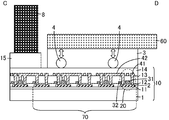
- FIG. FIG. 2 is a schematic cross-sectional view of the circuit board according to the first embodiment, showing a cut surface taken along line AB of FIG.
- FIG. 2 is a schematic plan view of the circuit board according to the first embodiment, showing a cut surface taken along line CD in FIG. 1.
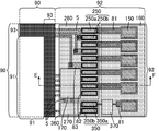
- 6 is a schematic plan view of a circuit board according to Embodiment 2.
- FIG. FIG. 5 is a schematic cross-sectional view of a circuit board according to Embodiment 2, showing a cut surface taken along the line EF of FIG. 6 is a schematic plan view of a circuit board according to Embodiment 3.
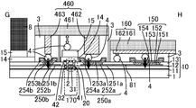
- FIG. 10 is a schematic cross-sectional view of a circuit board according to Embodiment 3, showing a cut surface taken along the line GH of FIG. 7 is a schematic plan view of a circuit board of Reference Example 1.
- FIG. 9 is a schematic cross-sectional view of the circuit board of Reference Example 1 and shows a cut surface taken along line IJ in FIG. 8.
- FIG. 1 is a schematic plan view of a circuit board according to the first embodiment.
- the circuit board of Embodiment 1 is a first circuit board of the present invention in that it includes a transistor substrate having a transistor and an external connection terminal.
- the circuit wiring board having a circuit wiring including a fine circuit wiring and an external connection terminal is provided.
- the circuit board according to the first embodiment includes a display area 90 and a peripheral circuit area 92.
- the display area 90 includes a pixel area 91 and a seal area 93 that surrounds the pixel area 91. Since the circuit board of Embodiment 1 has circuits formed in both the display area 90 and the peripheral circuit area 92, a circuit that controls the display element and a peripheral circuit that controls the circuit that controls the display element Are full monolithic circuit boards provided on one support substrate.
- the peripheral circuit region 92 includes the external member 60, the transistor circuit board 10 on which a plurality of circuits are mounted on one support substrate, and the external member connected to the transistor circuit board 10 are provided. 60 is also a circuit board composed of 60. Since the display region 90 that can control the display element and the peripheral circuit region 92 that controls the display region 90 are configured on one transistor circuit substrate 10 as described above, The circuit board is suitably used as a substrate for a display device.
- a plurality of external connection terminals 50 connected to the external member 60 are arranged side by side in the peripheral circuit region 92, and are arranged along a boundary line between the display region 90 and the peripheral circuit region 92. .
- a circuit including a circuit wiring and a transistor (hereinafter also referred to as a transistor circuit) 70 is connected to each external connection terminal 50 via a terminal lead-out wiring 80, and the external connection terminal 50 is connected via the transistor circuit 70.
- a transistor circuit 70 are connected to the pixel region 91 constituting the display region 90.
- the transistor circuits 70 are also provided side by side, and form a column along the boundary line between the display region 90 and the peripheral circuit region 92.
- the plurality of transistor circuits 70 are integrated in the vicinity of the boundary line between the display area 90 and the peripheral circuit area 92.
- the type of the transistor circuit 70 formed in the peripheral circuit region 92 is not particularly limited.
- a driver circuit including a circuit such as a transmission gate, a latch circuit, a timing generator, and a power supply circuit, a buffer circuit, a digital-analog conversion
- Examples of the circuit include a circuit (DAC circuit), a shift register, and a sampling memory.
- Examples of the driver circuit include a source driver circuit and a gate driver circuit. Since the external connection terminal 50 and the transistor circuit 70 are arranged side by side in this way, they are not substantially overlapped with each other.
- both the external connection terminal 50 and the transistor circuit 70 form a column along the boundary line between the display region 90 and the peripheral circuit region 92, but these are alternately arranged side by side.
- One composite row composed of the circuit 70 and the external connection terminal 50 is formed.
- the column including the external connection terminal 50 and the transistor circuit 70 is configured in a region closer to the display region 90 in the peripheral circuit region 92 in order to reduce the area of the peripheral circuit region 92.
- the transistor circuit 70 needs to have a larger area than the external connection terminal 50 and is formed so as to extend to the frame side away from the display region 90 side.
- the external connection terminals 50 and the transistor circuits 70 are alternately formed side by side in consideration of the restriction that the external connection terminals 50 and the transistor circuits 70 are arranged side by side so that they do not overlap each other. Then, it can be said that it is an efficient arrangement form in that the area (frame area) of the peripheral circuit region 92 is reduced.
- the external connection elements 50 are each configured using a conductive member, and can be electrically connected to each other by overlapping with the conductive member included in the external member 60.
- the external member 60 is a flexible printed circuit board (FPC) 60 having conductive protrusions (bumps or external connection wiring).
- FPC flexible printed circuit board
- an electronic component composed of circuit elements such as a resistor, a capacitor, a coil, a connector, a diode, and a transistor, or an integrated circuit including these circuit elements. Examples include a chip (COG or COF) on which a circuit (IC) is mounted.
- COG or COF on which a circuit (IC) is mounted.
- Other examples include a printed wiring board (PWB), a printed circuit board (PCB), and a tape carrier package (TCP).
- any of the external connection terminals 50 and the transistor circuit 70 are flexible connected to the external connection terminals 50 when viewed from a direction perpendicular to the main surface of the transistor circuit substrate 10.
- a printed circuit board (FPC) 60 is arranged to overlap. Thereby, the area (frame area) of the peripheral circuit region 92 can be effectively reduced.
- the external connection terminal 50 and the transistor circuit 70 are arranged side by side, that is, do not substantially overlap each other when viewed from a direction perpendicular to the main surface of the transistor circuit board 10. Are arranged as follows.
- the seal area 93 is an area where a sealing member for bonding a plurality of members constituting the display element to each other is used, and is an area that does not actually contribute to display.
- the pixel area 91 of the display area 90 is an area where pixels, which are a plurality of small units constituting the display area 90, are formed, and is an area that actually contributes to display.
- a plurality of pixels are formed in the display region 90, and each pixel is driven and controlled by a transistor circuit formed in the pixel region 91, whereby a good display with high precision can be obtained.
- the transistor circuit 70 formed in the peripheral circuit region 92 can be a driver block circuit that further controls the drive control of the pixel region 91.
- FIG. 2 is a schematic cross-sectional view of the circuit board according to the first embodiment, and shows a cut surface taken along the line AB of FIG.
- the cut surface along the line AB includes external connection terminals.
- the transistor circuit substrate 10 has a base coat film (first insulating film) 11 formed on one surface on a support substrate 1, on which various wirings, transistors, and external connection terminals are formed. Etc. are appropriately arranged through an insulating film.
- a material having an insulating film is preferably used, and examples thereof include glass and resin.
- the support substrate 1 may be one in which an insulating film is formed on the surface of a conductive base material.
- the transistor As the transistor, a thin film transistor (TFT) 20 that is a three-terminal field effect transistor (FET) is used.
- the transistor circuit substrate 10 includes a plurality of TFTs 20, and each of the plurality of TFTs 20 includes a semiconductor layer 2 and three electrodes of a gate electrode 31, a source electrode, and a drain electrode.
- a gate insulating film (second insulating film) 12 is formed between the semiconductor layer 2 and the gate electrode 31, and the semiconductor layer 2, the second insulating film 12, and the gate electrode 31 are formed from the support substrate 1 side. These are laminated in order.
- a circuit wiring 32 made of the same material as the gate electrode 31 is formed at a position beside the TFT 20 in the same layer as the layer where the gate electrode 31 is disposed.
- An inorganic interlayer insulating film (third insulating film) 13 is further formed on the gate electrode 31 in one or more layers.
- the source electrode and the drain electrode 41 are disposed on the third insulating film 13 through a contact hole provided in a multilayer insulating film composed of the second insulating film 12 and the third insulating film 13.
- the semiconductor layer 2 is electrically connected.
- the source and drain electrodes 41 are partially extended to form circuit wirings 42 and connect adjacent TFTs.
- the TFT 20 is connected to the external connection terminal 50 through a terminal lead wiring 80 extended from the source electrode or drain electrode 41.
- the insulating film on the source and drain electrodes 41 is the organic interlayer insulating film (fourth insulating film) 14, and the organic interlayer insulating film (fifth insulating film) 15 is formed on the fourth insulating film 14.
- a seal member 8 is disposed on the fifth insulating film 15.
- the external connection terminal 50 is configured by a stacked body in which a plurality of conductive films are stacked.
- the stacked body of the external connection terminals 50 included in the transistor circuit substrate 10 is stacked in the order of aluminum (Al) and molybdenum (Mo) or indium zinc oxide (IZO) from the support substrate 1 side.
- the first conductive film 51 and the second conductive film 52 made of indium tin oxide (ITO) are laminated, and other circuit elements in the peripheral circuit region, or The same materials as those used for the circuit elements in the pixel region (Al, Mo, IZO) and the pixel electrode (ITO) are used.
- the circuit wiring and a part of the stacked body of the external connection terminals can be formed at the same time in the same process, which can be said to be an efficient configuration.
- the external connection terminals are designed to have a width of 300 to 3000 ⁇ m in the vertical direction and 20 to 300 ⁇ m in the horizontal direction when viewed from the direction perpendicular to the main surface of the substrate.
- the line width of the terminal lead-out wiring 80 is 5 to 350 ⁇ m when viewed from the direction perpendicular to the main surface of the substrate.
- the external connection terminal 50 is connected to the FPC 60 that is an external member.
- the FPC 60 includes a support substrate 61 and bumps (conductive protrusions) 62 formed on the support substrate 61.
- the FPC 60 has a bump 62 in a region overlapping with the external connection terminal 50, and a difference for physically and electrically connecting the bump 62 and the external connection terminal 50 between the bump 62 and the external connection terminal 50.
- An anisotropic conductive film (ACF) 3 and conductive fine particles 4 are arranged.
- the ACF 3 is arranged so that the external connection terminals 50 are not electrically connected to each other.
- the bumps 62 included in the FPC 60 according to the first embodiment are wirings included in the FPC 60, and include, for example, copper (Cu), gold (Au), or the like.
- the line width of the wiring (bump) 62 is 20 to 300 ⁇ m when viewed from a direction perpendicular to the main surface of the substrate.
- the thickness of the wiring (bump) is 1 to 50 ⁇ m.
- ACF3 for example, a resin composition containing a resin such as epoxy and acrylic and a thermosetting reaction agent, a conductive ball obtained by plating a resin ball having a diameter of about 2 to 10 ⁇ m with nickel (Ni), gold (Au), or the like. That contain the conductive fine particles 4 at a certain ratio can be used.
- ACF3 functions as an adhesive. Therefore, by applying the ACF 3 between the external connection terminal 50 provided in the transistor circuit board 10 and the bump 62 provided in the FPC 60 and applying a constant pressure while applying a constant heat, so-called thermocompression bonding is performed.
- the transistor circuit board 10 and the FPC 60 are electrically and physically connected.
- the external connection terminal 50 and the FPC 60 can be integrated by, for example, crimping.
- the external connection terminal 50, the ACF 3, and the bump 62 have three overlapping portions.
- the column supports the transistor circuit board 10 and the FPC (external member) 60, and the greatest pressure is applied in this region.
- the portion to be the support is the portion having the shortest distance among the distances between the transistor circuit board 10 and the FPC 60.
- the conductive fine particles 4 in the ACF 3 located in the region overlapping with the external connection terminals are As shown in FIG.
- the shape becomes elliptical due to the pressure, and a certain amount of pressure is applied to the external connection terminal 50 in the direction of the black arrow in FIG. 2.
- the external connection terminal 50 are arranged side by side, and are arranged so as not to substantially overlap each other, so that a short circuit of the circuit wiring that may be caused by the pressure bonding between the transistor substrate 10 and the FPC 60, and the transistor Deterioration of the 20 characteristics can be suppressed.
- FIG. 3 is a schematic cross-sectional view of the circuit board according to the first embodiment, showing a cut surface taken along line CD in FIG.
- the cut surface by the CD line includes a circuit wiring and a transistor.
- the transistor circuit substrate 10 includes a transistor circuit 70 including a plurality of transistors 20, and the FPC 60 is disposed at a position overlapping the transistor circuit 70.
- the ACF 3 is formed between the transistor circuit board 10 and the FPC 60, but the distance between the transistor circuit board 10 and the FPC 60 in the region overlapping the transistor 20 is the transistor circuit in the region overlapping the external connection terminal 50. The distance is shorter than the distance between the substrate 10 and the FPC 60. Therefore, as indicated by the white arrow in FIG.
- FIG. 4 is a schematic plan view of the circuit board according to the second embodiment.
- the circuit board of the second embodiment is a first circuit board of the present invention in that it includes a transistor substrate having a transistor and an external connection terminal.
- the circuit wiring board having a circuit wiring including a fine circuit wiring and an external connection terminal is provided.
- the circuit board according to the second embodiment includes a display area 90 and a peripheral circuit area 92.
- the display area 90 includes a pixel area 91 and a seal area 93 that surrounds the pixel area 91. Since the circuit board of the second embodiment has circuits formed in both the display area 90 and the peripheral circuit area 92, a circuit that controls the display element and a peripheral circuit that controls the circuit that controls the display element Are fully monolithic circuit boards provided on one support substrate.
- a flexible printed circuit board (FPC) 160 In the peripheral circuit region 92, three external members, a flexible printed circuit board (FPC) 160, a COG 260 on which an IC is mounted, and a single electronic component such as a resistor, a capacitor, a coil, a connector, a diode, and a transistor 360 includes the transistor circuit board 10 in which a plurality of circuits are mounted on one support substrate, and an external member connected to the transistor circuit board 10. Since the display region 90 that can control the display element and the peripheral circuit region 92 that controls the display region 90 are configured on one transistor circuit substrate 10 as described above, the second embodiment This circuit board is suitably used as a substrate for a display device.
- FPC flexible printed circuit board
- the external connection terminals included in the circuit board of Embodiment 2 are the first external connection terminal 150 connected to the FPC 160, the second external connection terminal 250 connected to the COG 260, and the third external terminal connected to the electronic component 360. And the external connection terminal 350.
- the plurality of external connection terminals 150, 250, 350 are arranged side by side, and form a plurality of columns along the boundary line between the display region 90 and the peripheral circuit region 92. Arranging the external connection terminals 150, 250, and 350 in a row in this manner is preferable from the viewpoint of improving the degree of integration and reducing the frame area.
- two rows composed of external connection terminals are arranged.
- both of these two rows are arranged along one side of each of the external members 160, 260, and 360.
- the row of external connection terminals located closer to the frame side of the transistor circuit board 10 is composed of the first external connection terminals 150, and the external connection terminals located closer to the display area 90 of the transistor circuit board 10.
- the row includes a second external connection terminal 250 and a third external connection terminal 350.
- each external member is disposed so as to overlap with each external connection terminal, a narrow frame is realized.
- these external connection terminal rows are all arranged in a straight line, but may be arranged in a zigzag shape (zigzag shape), for example, as long as they form a series of rows.
- a first terminal lead-out wiring 81 is provided between the first external connection terminal 150 and the second external connection terminal 250 or the third external connection terminal 350.
- the first terminal lead-out wiring 81 is a wiring extended from the first external connection terminal 150 in the direction of the pixel region 91.
- two circuits including transistors along with circuit wiring are formed side by side along a boundary line between the display region 90 and the peripheral circuit region 92.
- One of them is a transistor circuit (hereinafter, also referred to as a first transistor circuit) 170 disposed so as to overlap with the COG 260, and the other is a transistor circuit (hereinafter referred to as a second transistor circuit) disposed so as to overlap with the electronic component 360. 270).
- a routing wiring 5 is formed between the first transistor circuit 170 and the second transistor circuit 270, and can be connected to each other to form one large circuit.
- a transistor circuit (hereinafter also referred to as a third transistor circuit) 370 is formed between the first external connection terminal 150 and the third external connection terminal 350.
- the third transistor circuit 370 the first terminal lead-out wiring 81 is divided into two.
- the type of transistor circuit formed in the peripheral circuit region 92 is not particularly limited.
- a driver circuit including an inverter and other circuits such as a transmission gate, a latch circuit, a timing generator, and a power supply circuit, a buffer circuit and a digital-analog conversion circuit (DAC circuit), a shift register, a sampling memory, and the like can be given.
- Examples of the driver circuit include a source driver circuit and a gate driver circuit.
- the second external connection terminal 250 is connected to another adjacent second external connection terminal 250 via the COG 260.
- the second external connection terminal directly connected to the first terminal lead-out wiring 81 is the input external connection terminal 250a, and the other adjacent second external connection terminal is the output external connection terminal 250b.
- the second external connection terminal (output external connection terminal) 250b includes a second terminal lead-out wiring 82 extending from the second external connection terminal (output external connection terminal) 250b toward the pixel region 91. And is connected to the first transistor circuit 170.
- the first transistor circuit 170 is connected to the pixel region 91 by the lead wiring 5 extended from the first transistor circuit 170.
- a plurality of lead wirings 5 are extended from the first transistor circuit 170 toward the pixel region 91 in a straight line (with the shortest distance).
- the third external connection terminal 350 is connected to another adjacent third external connection terminal 350 via the electronic component 360.
- the third external connection terminal directly connected to the first terminal lead-out wiring 81 is the input external connection terminal 350a, and the other adjacent third external connection terminal is the output external connection terminal 350b.
- the third external connection terminal (output external connection terminal) 350b includes a second terminal lead-out wiring 82 extending from the third external connection terminal (output external connection terminal) 350b toward the pixel region 91. And is connected to the second transistor circuit 270.
- the second transistor circuit 270 is connected to the pixel region 91 by the lead wiring 5 extended from the second transistor circuit 270. From the second transistor circuit 270, the lead wiring 5 is extended in a straight line (with the shortest distance) toward the pixel region.
- the first external connection terminal 150 is designed to have a width of 300 to 3000 ⁇ m in the vertical direction and 20 to 300 ⁇ m in the horizontal direction when viewed from the direction perpendicular to the main surface of the substrate.
- the second external connection terminal 250 and the third external connection terminal 350 are both 50 to 500 ⁇ m in the vertical direction and 20 to 100 ⁇ m in the horizontal direction when viewed from the direction perpendicular to the main surface of the substrate. Designed with width.
- the second external connection terminal 250 and the third external connection terminal 350 are compared, their areas are comparable, and the first external connection terminal 150, the second external connection terminal 250, and the third external connection terminal are the same.
- the area of the first external connection terminal 150 is larger.
- the second external connection terminal 250 and the third external connection terminal 350 have input external connection terminals 250a and 350a and output external connection terminals 250b and 350b arranged side by side and alternately.
- they are collected and arranged on the frame side of the COG (on the opposite side to the pixel region 91), it is easy to design the circuit so as to be directed in one direction, which improves the degree of integration and reduces the frame region. It can be further planned.
- the lead-out wiring 5 is a fine circuit wiring, and is arranged side by side with the external connection terminal so that it does not substantially overlap with the external connection terminal.
- conductive fine particles in an anisotropic conductive film (ACF) are used as the conductive member, and this single conductive fine particle constitutes one conductive member.
- the conductive member has such a width that it can cross the routing wiring (fine circuit wiring) 5 when it is overlapped with the routing wiring (fine circuit wiring) 5.
- the width of the conductive member is about 2 to 10 ⁇ m.
- the frame area can be reduced.
- the line width of the narrow portion of the routing wiring 5 in the second embodiment is 2 to 3 nm.
- the lead-out wiring 5 is designed so as to be bent at a right angle after being extended by a certain length and to be collected at an appropriate portion of the pixel region 91.
- the third terminal lead-out wiring 83 extended from the second external connection terminal (output external connection terminal) 250b has a second extension extending from the other adjacent second external connection terminal (output external connection terminal) 250b. The extension length differs from that of the third terminal lead-out wiring 83. By changing the length in this way, the routing wiring 5 can be efficiently formed, and the degree of integration is improved and the frame area is reduced.
- the pixel area is connected from the FPC 160 through the following three types of paths.
- the first path is from the FPC 160 to the first external connection terminal 150, the first terminal lead-out wiring 81, the second external connection terminal (input external connection terminal) 250a, the COG 260, and the second external connection terminal (output).
- the second path is from the FPC 160 to the first external connection terminal 150, the first terminal lead-out wiring 81, the second external connection terminal (input external connection terminal) 250a, the COG 260, and the second external connection terminal (output).
- the third path is from the FPC 160 to the first external connection terminal 150, the first terminal lead wiring 81, the third transistor circuit 370, the first terminal lead wiring 81, and the third external connection terminal (external input).
- the transistor circuit and the external connection terminal are arranged side by side, and are arranged so as not to overlap each other when viewed from a direction perpendicular to the main surface of the transistor circuit substrate.
- a plurality of pixels are formed in the pixel region 91, and a wiring extending from the peripheral circuit region is connected to each pixel. Therefore, a plurality of wirings are arranged in the pixel region.
- a transistor may be provided in each wiring as appropriate in the pixel region.
- the transistor functions as a switching element for driving the pixel.
- the first transistor circuit 170 and the second transistor circuit 270 formed in the peripheral circuit region can be driver block circuits that further control the drive control of the pixel region 91.
- FIG. 5 is a schematic cross-sectional view of the circuit board according to the second embodiment, and shows a cut surface taken along the line EF of FIG.
- the transistor circuit substrate 10 has a base coat film (first insulating film) 11 formed on one surface on a support substrate 1, on which various wirings, transistors, and external connection terminals are formed. Etc. are appropriately arranged through an insulating film.
- a material having an insulating film is preferably used, and examples thereof include glass and resin.
- the support substrate 1 may be one in which an insulating film is formed on the surface of a conductive base material.
- a thin film transistor (TFT) 20 that is a three-terminal field effect transistor (FET) is used.
- the transistor circuit substrate 10 includes a plurality of TFTs 20, and each of the plurality of TFTs 20 includes a semiconductor layer 2 and three electrodes, that is, a gate electrode 31, a source electrode, and a drain electrode.
- a gate insulating film (second insulating film) 12 is formed between the semiconductor layer 2 and the gate electrode 31, and the semiconductor layer 2, the second insulating film 12, and the gate electrode 31 are formed from the support substrate 1 side. These are laminated in order.
- a circuit wiring 32 made of the same material as the gate electrode 31 is formed at a position beside the TFT 20 in the same layer as the layer where the gate electrode 31 is disposed.
- An inorganic interlayer insulating film (third insulating film) 13 is further formed on the gate electrode 31 in one or more layers.
- the source electrode and the drain electrode 41 are disposed on the third insulating film 13 through a contact hole provided in a multilayer insulating film composed of the second insulating film 12 and the third insulating film 13.
- the semiconductor layer 2 is electrically connected.
- a circuit wiring 42 made of the same material as that of the source and drain electrodes 41 is formed at a position beside the TFT in the same layer as the layer where the source and drain electrodes 41 are disposed.
- a part of the circuit wiring 42 is extended to form the routing wiring 5 and is connected to the pixel region 91.
- the insulating film on the source and drain electrodes 41 is the organic interlayer insulating film (fourth insulating film) 14, and the organic interlayer insulating film (fifth insulating film) 15 is formed on the fourth insulating film 14.
- a seal member 8 is disposed on the fifth insulating film 15.
- TFT upper circuit wiring 45 is disposed, and adjacent TFTs 20 are connected through contact holes provided in the fourth insulating film 14.
- the external connection terminals provided in the transistor circuit board of Embodiment 2 are the three types of the first external connection terminal 150, the second external connection terminal 250, and the third external connection terminal 350, and are based on the EF line.
- the cut surface includes a first external connection terminal 150 and a second external connection terminal 250.
- Each of the first external connection terminal 150 and the second external connection terminal 250 is configured by a stacked body in which a plurality of conductive films are stacked.
- the stacked body includes the material constituting the TFT 20 and the circuit wirings 32 and 42 described above, and the conductive film 251 including the material constituting the gate electrode 31, the source electrode and the drain electrode 41 from the support substrate 1 side.
- the conductive film 252 including the material constituting the conductive film 252, the conductive film 253 including the material constituting the TFT upper wiring 45, and the transparent conductive film 254 used for the pixel region 91 are stacked in this order.
- the external connection terminals 150, 250, and 350 included in the transistor circuit substrate 10 of Embodiment 2 may include a conductive film formed of a material other than these.
- the conductive film 251 containing a material constituting the gate electrode has a structure in which a tantalum (Ta) layer and a tungsten (W) layer are stacked in this order from the support substrate 1 side.
- the film thickness of the tantalum (Ta) layer is 50 nm
- the film thickness of the tungsten (W) layer is 350 nm.
- the conductive film 252 including a material constituting the source and drain electrodes 41 has a structure in which a titanium (Ti) layer, an aluminum (Al) layer, and a titanium (Ti) layer are stacked in this order from the support substrate 1 side.
- the (Ti) layer has a thickness of 100 nm
- the aluminum (Al) layer has a thickness of 500 nm.
- the conductive film 253 containing the material constituting the TFT upper wiring 45 has a structure in which an aluminum (Al) layer and a molybdenum (Mo) layer are stacked in this order from the support substrate 1 side, and the film thickness of the aluminum (Al) layer is The film thickness of the 400 nm, molybdenum (Mo) layer is 100 nm.
- the transparent conductive film 254 used in the pixel region 91 is composed of an ITO layer, and the thickness of the ITO layer is 100 nm.
- the external connection terminals 150 and 250 formed by stacking the conductive films can secure a certain amount of film thickness for shortening the distance between the external members 160 and 260 and the transistor circuit substrate 10. .
- the region overlapping with the external connection terminals 150 and 250 can be a portion having the shortest distance among the distances between the transistor circuit board 10 and the FPC 160 or the COG 260.
- the external connection terminals 150 and 250 formed by stacking the conductive films in Embodiment 2 are made of materials used for other components such as a transistor circuit and a pixel electrode, and therefore their manufacturing processes are There is no need to perform a separate manufacturing process, which is efficient.
- the FPC 160 includes a support substrate 161 and external connection wiring (conductive protrusions) 162 formed on the support substrate 161.
- the COG 260 includes a support substrate 261 and bumps (conductive protrusions) 262 formed on the support substrate 261.
- the first external connection terminal 150 is connected to the FPC 160, and the second external connection terminal 250 is connected to the COG 260.
- the external connection terminal 150 and the FPC 160 are arranged between the external connection wiring 162 and the external connection terminal 150, and are anisotropic for physically and electrically connecting the external connection wiring 162 and the external connection terminal 150. They are connected to each other through a conductive film (ACF) 3 and conductive fine particles 4.
- ACF conductive film
- the external connection terminal 250 and the COG 260 are disposed between the bump 262 and the external connection terminal 250, and are an anisotropic conductive film for physically and electrically connecting the bump 262 and the external connection terminal 250. They are connected via (ACF) 3 and conductive fine particles 4.
- the ACF 3 is arranged so that the external connection terminals 150, 250, 350 are not electrically connected to each other.
- solder can be used instead of the conductive fine particles 4 in the ACF 3.
- the external connection wiring 162 included in the FPC 160 is a wiring formed on the support substrate 161, and is made of, for example, copper (Cu), gold (Au), or the like.
- the bumps 262 included in the COG 260 are electrodes formed on the support substrate 261, and are made of, for example, copper (Cu), gold (Au), or the like.
- the width of the external connection wiring 162 connected to the first external connection terminal 150 is 50 to 300 ⁇ m when viewed in the vertical direction from the main surface of the substrate, and the thickness of the external connection wiring 162 is 1 to 100 ⁇ m. is there.
- the width of the bump 262 connected to the second external connection terminal 250 is 1 to 100 ⁇ m when viewed from the direction perpendicular to the main surface of the substrate, and the thickness of the bump 262 is 2 to 10 ⁇ m. It is.
- a dedicated electrode or wiring newly provided on the external member may be newly used, or an electrode or wiring originally provided in the external member may be used as it is.
- ACF3 for example, a resin composition of a resin such as epoxy or acrylic and a thermosetting reaction agent, a resin ball having a diameter of about 2 to 10 ⁇ m and plated with nickel (Ni), gold (Au) or the like is used. What contains the microparticles
- ACF3 functions as an adhesive. Therefore, the ACF 3 is attached between the external connection terminals 150 and 250 included in the transistor circuit board 10 and the external connection wiring 162 included in the FPC 160 and the bump 262 included in the COG 260, and these are pressed against each other while applying a certain amount of heat.
- thermocompression bonding the transistor circuit board 10 and the FPC 160 and COG 260 are electrically and physically connected.
- the external connection terminals 150 and 250, the FPC 160, and the COG 260 can be integrated by, for example, crimping.
- the external connection terminal 150, the ACF 3, and the external connection wiring 162 The overlapping portions and the portions where the external connection terminals 250, ACF 3 and bumps 262 overlap are the pillars for connecting the FPC 160 and COG 260 and the transistor circuit board 10, respectively.
- the greatest pressure is applied in the direction of the black arrow.
- characteristic degradation may occur in the fine circuit wiring and the transistor in the transistor circuit 170 due to the pressure at the time of crimping.
- the transistor circuit 170 and the external connection terminals 150 and 250 are arranged side by side and are arranged so as not to substantially overlap each other, the crimping between the external connection terminals 150 and 250 and the FPC 160 or the COG 260 is a factor. Short circuit of the fine circuit wiring that can occur and deterioration of the characteristics of the transistor can be suppressed.
- the COG 260 is disposed in a region overlapping with the transistor circuit 170. Further, the FPC 160 is arranged in a region overlapping with the first terminal lead-out line 81 extended from the first external connection terminal 150. An ACF 3 is also formed between the transistor circuit substrate 10 and the FPC 160 and COG 260 in the region overlapping with these transistor circuits and the region overlapping with the terminal lead-out wiring. There is enough space with a height greater than the particle size. Therefore, even if the FPC 160 and the COG 260 are pressure-bonded to the external connection terminals 150 and 250, the pressure applied to the transistor circuit substrate 10, that is, the transistor circuit 170 and the terminal lead-out wiring (circuit wiring) 81 formed thereunder. There is little load.
- the external connection terminals 150 and 250 and the FPC 160 are disposed in the region where the transistor circuit 170 is disposed. Or it is not necessary to apply the pressure equivalent to the magnitude
- dummy bumps 263 having a size smaller than the support bumps 262 are provided on the fifth insulating film 15 in a region overlapping with the COG 260.
- the width of the dummy bump 263 is 2 to 20 ⁇ m when viewed from the direction perpendicular to the main surface of the substrate, and the thickness of the dummy bump 263 is 5 to 20 ⁇ m.
- the dummy bumps 263 are provided as sub-pillars for the COG 260 to be disposed in parallel with the transistor circuit board 10 in a well-balanced manner with respect to the transistor circuit substrate 10 with respect to the bumps 262 located in the region overlapping with the external connection terminals 250 serving as main pillars. It is. Note that the dummy bumps 263 are not arranged via the ACF 3. Therefore, there is little influence that the conductive fine particles 4 in the ACF are pressed by the dummy bumps at the time of pressure bonding by the dummy bumps.
- FIG. 6 is a schematic plan view of the circuit board according to the third embodiment.
- the circuit board of the third embodiment is a first circuit board of the present invention in that it includes a transistor substrate having a transistor and an external connection terminal.
- the circuit wiring board having a circuit wiring including a fine circuit wiring and an external connection terminal is provided.
- the circuit board according to the third embodiment includes a display area 90 and a peripheral circuit area 92.
- the display area 90 includes a pixel area 91 and a seal area 93 that surrounds the pixel area 91. Since the circuit board of the third embodiment has circuits formed in both the display area 90 and the peripheral circuit area 92, a circuit that controls the display element and a peripheral circuit that controls the circuit that controls the display element Are fully monolithic circuit boards provided on one support substrate.
- the peripheral circuit region 92 In the peripheral circuit region 92, three external members, a flexible printed circuit board (FPC) 160, a COG 460 on which an IC is mounted, and a single electronic component such as a resistor, a capacitor, a coil, a connector, a diode, and a transistor 560 is provided, it is also a circuit board constituted by the transistor circuit board 10 in which a plurality of circuits are mounted on one supporting board and an external member connected to the transistor circuit board 10. Since the display region 90 that can control the display element and the peripheral circuit region 92 that controls the display region 90 are configured on one transistor circuit substrate 10 as described above, the third embodiment This circuit board is suitably used as a substrate for a display device.
- FPC flexible printed circuit board
- the external connection terminals included in the circuit board of Embodiment 3 are the first external connection terminal 150 connected to the FPC 160, the second external connection terminal 250 connected to the COG 460, and the third external terminal connected to the electronic component 560. And the external connection terminal 350.
- the plurality of external connection terminals 150, 250, and 350 are arranged side by side, and form a plurality of columns along the boundary line between the display region 90 and the peripheral circuit region 92. .
- three rows composed of external connection terminals are arranged. Further, all of these three rows are arranged along one side of each of the external members 160, 460, 560.
- the column located on the most frame side of the transistor circuit board 10 is configured by the first external connection terminals 150, and the two columns positioned on the display area 90 side are the second external connection terminals 250 and the first external connection terminals 150. It consists of three external connection terminals 350.
- each external member is arranged so as to overlap with the external connection terminal in this way, narrowing of the frame is realized.
- these external connection terminal rows are all arranged in a straight line, but may be arranged in a zigzag shape (zigzag shape), for example, as long as they form a series of rows.
- a first terminal lead-out wiring 81 is provided between the first external connection terminal 150 and the second external connection terminal 250 or the third external connection terminal 350.
- the first terminal lead-out wiring 81 is a wiring extended from the first external connection terminal 150 in the direction of the pixel region.
- two circuits including transistors along with circuit wiring are formed side by side along a boundary line between the display region 90 and the peripheral circuit region 92.
- One of them is a first transistor circuit 170 disposed so as to overlap with the COG 460, and the other is a second transistor circuit 270 disposed so as to overlap with the electronic component 560.
- a routing wiring 5 is formed between the first transistor circuit 170 and the second transistor circuit 270, and can be connected to each other to form one large circuit.
- a third transistor circuit 370 is formed between the first external connection terminal 150 and the third external connection terminal 350, whereby the first terminal lead-out wiring 81 is divided into two. Has been.
- the type of transistor circuit formed in the peripheral circuit region 92 is not particularly limited.
- a driver circuit including an inverter and other circuits such as a transmission gate, a latch circuit, a timing generator, and a power supply circuit, a buffer circuit and a digital-analog conversion circuit (DAC circuit), a shift register, a sampling memory, and the like can be given.
- Examples of the driver circuit include a source driver circuit and a gate driver circuit.
- the second external connection terminal 250 is connected to another second external connection terminal facing each other with the first transistor circuit 170 interposed therebetween via the COG 460.
- the second external connection terminal directly connected to the first terminal lead-out line 81 is the input external connection terminal 250a, and the other second external connection terminal facing the output external connection terminal 250b.
- the second external connection terminal (output external connection terminal) 250b extends from the second external connection terminal (output external connection terminal) 250b in the frame direction (the direction opposite to the pixel region).
- the first transistor circuit 170 is connected via the terminal lead-out wiring 82.
- the first transistor circuit 170 is connected to the pixel region 91 by the lead wiring 5 connected to the first transistor circuit 170.
- a plurality of lead wirings 5 are extended from the first transistor circuit 170 toward the pixel region 91 in a straight line (with the shortest distance).
- the third external connection terminal 350 is connected to another third external connection terminal facing each other with the second transistor circuit 270 interposed therebetween via the electronic component 560.
- the third external connection terminal directly connected to the first terminal lead-out wiring 81 is the input external connection terminal 250a
- the other third external connection terminal facing the external connection terminal 250b is the output external connection terminal 250b.
- the third external connection terminal (output external connection terminal) 350b is a second external terminal extended from the third external connection terminal (output external connection terminal) 350a in the frame direction (the direction opposite to the pixel region). It is connected to the second transistor circuit 270 through the terminal lead-out wiring 82.
- the second transistor circuit 270 is connected to the pixel region 91 by the lead wiring 5 connected to the second transistor circuit 270.
- a plurality of lead wirings 5 are extended from the second transistor circuit 270 toward the pixel region 91 in a straight line (with the shortest distance).
- the first external connection terminal 150 is designed to have a width of 300 to 3000 ⁇ m in the vertical direction and 20 to 300 ⁇ m in the horizontal direction when viewed from the direction perpendicular to the main surface of the substrate.
- the second external connection terminal 250 and the third external connection terminal 350 are both in the vertical direction when viewed from the direction perpendicular to the substrate main surface with respect to the input external connection terminals 250a and 350a.
- the width is designed to be 400 to 800 ⁇ m and 100 to 300 ⁇ m in the lateral direction.
- the output external connection terminals 250b and 350b are designed to have a width of 100 to 200 ⁇ m in the vertical direction and 20 to 40 ⁇ m in the horizontal direction when viewed from the direction perpendicular to the main surface of the substrate.
- the input external connection terminals 250a and 350a have the same area, and the output external connection terminals 250b and 350b also have the same area. These areas are comparable.
- the input external connection terminals 250a and 350a are compared with the output external connection terminals 250b and 350b, the area of the input external connection terminals 250a and 350a is larger.
- the first external connection terminal 150 is compared with the second external connection terminal 250 and the third external connection terminal 350, the area of the first external connection terminal 150 is larger.
- the second external connection terminal (output external connection terminals) 250b are connected to the pixel region 91 without passing through the transistor circuit.
- the second external connection terminal (output external connection terminal) 250b connected to the pixel region 91 without going through the transistor circuit is connected to the third terminal lead wiring 83 and the third terminal lead wiring 83. It is connected to the pixel region 91 through the wiring 5.
- the third terminal lead-out wiring 83 extended from the second external connection terminal (output external connection terminal) 250b extends in the frame direction (the direction opposite to the pixel region), and therefore the third terminal
- the lead-out wiring 5 connected to the lead-out wiring 83 is bent at a right angle of 2 degrees and bypasses the second external connection terminal (output external connection terminal) 250b, thereby being collected at an appropriate portion of the pixel region 91.
- the design is made.
- the routing wiring 5 is once extended from the external connection terminal in a direction away from the pixel region 91 (display region 90), passes through two bent portions, and goes to the pixel region 91 (display region 90). Stretched.
- the lead-out wiring 5 is a fine circuit wiring, and is arranged side by side with the external connection terminal so that it does not substantially overlap with the external connection terminal.
- conductive fine particles in an anisotropic conductive film (ACF) are used as the conductive member, and this single conductive fine particle constitutes one conductive member.
- the conductive member has such a width that it can cross the routing wiring (fine circuit wiring) 5 when it is overlapped with the routing wiring (fine circuit wiring) 5.
- the width of the conductive member is about 2 to 10 ⁇ m.
- the pixel area is connected from the FPC 160 through the following three types of paths.
- the first path is from the FPC 160 to the first external connection terminal 150, the first terminal lead-out wiring 81, the second external connection terminal (input external connection terminal) 250a, the COG 460, and the second external connection terminal (output).
- the second path is from the FPC 160 to the first external connection terminal 150, the first terminal lead-out wiring 81, the second external connection terminal (input external connection terminal) 250a, the COG 460, and the second external connection terminal (output).
- the external connection terminal) 250b, the third terminal lead-out wiring 83, and the lead-out wiring 5 are connected to the pixel region.
- the third path is from the FPC 160 to the first external connection terminal 150, the first terminal lead wiring 81, the third transistor circuit 370, the first terminal lead wiring 81, and the third external connection terminal (external input).
- Connection terminal) 250a, electronic component 560, third external connection terminal (output external connection terminal) 250b, third terminal lead wiring 83, second transistor circuit 270, and lead wiring 5 are connected to the pixel region. This is a route.
- the transistor circuit and the external connection terminal are arranged side by side so that they do not substantially overlap each other when viewed from the direction perpendicular to the main surface of the transistor circuit board.
- the external connection terminals are arranged side by side along one side of the external member.
- the external connection terminals connected to each other via the external member are opposed to each other across the transistor circuit.
- the external member is arranged so as to overlap with the circuit element such as a transistor, etc., which causes the external connection terminal and the external member to be crimped. It is possible to reduce the area of the peripheral circuit region while preventing short circuit of possible fine circuit wiring and deterioration of transistor characteristics.
- a plurality of pixels are formed in the pixel region 91, and wirings extending from the peripheral circuit region 92 are connected to the respective pixels. Therefore, a plurality of wirings are arranged in the pixel region 91.
- a transistor may be provided as appropriate for each wiring, and for example, it functions as a switching element for driving the pixel.
- the first transistor circuit 170 and the second transistor circuit 270 formed in the peripheral circuit region 92 can be driver block circuits that further control the drive control of the pixel region.
- FIG. 7 is a schematic cross-sectional view of the circuit board according to the third embodiment, showing a cut surface taken along the line GH of FIG.
- the transistor circuit substrate 10 has a base coat film (first insulating film) 11 formed on one surface on a support substrate 1, on which various wirings, transistors, and external connection terminals are formed. Etc. are appropriately arranged through an insulating film.
- a material having an insulating film is preferably used, and examples thereof include glass and resin.
- the support substrate 1 may be one in which an insulating film is formed on the surface of a conductive base material.
- the transistor As the transistor, a thin film transistor (TFT) 20 that is a three-terminal field effect transistor (FET) is used.
- the transistor circuit substrate 10 includes a plurality of TFTs 20, and each of the plurality of TFTs 20 includes a semiconductor layer 2 and three electrodes of a gate electrode 31, a source electrode, and a drain electrode.
- a gate insulating film (second insulating film) 12 is formed between the semiconductor layer 2 and the gate electrode 31, and the semiconductor layer 2, the second insulating film 12, and the gate electrode 31 are formed from the support substrate 1 side. These are laminated in order.
- Circuit wiring 32 made of the same material as the gate electrode is formed at a position beside the TFT in the same layer as the layer where the gate electrode 31 is disposed.
- An inorganic interlayer insulating film (third insulating film) 13 is further formed on the gate electrode 31 in one or more layers.
- the source electrode and the drain electrode 41 are disposed on the third insulating film 13 via a contact hole provided in a multilayer insulating film composed of the second insulating film 12 and the third insulating film 13.
- the semiconductor layer 2 is electrically connected.
- a circuit wiring 42 made of the same material as that of the source and drain electrodes 41 is formed at a position beside the TFT in the same layer as the layer where the source and drain electrodes 41 are disposed.
- the circuit wiring 42 is partially extended to form a TFT upper wiring, and adjacent TFTs are connected to each other.
- the insulating film 14 on the source and drain electrodes 41 is an organic interlayer insulating film (fourth insulating film), and the organic interlayer insulating film (fifth insulating film) 15 is formed on the fourth insulating film 14.
- a seal member 8 is disposed on the fifth insulating film 15.
- the external connection terminals provided in the transistor circuit board of Embodiment 3 are the three types of the first external connection terminal 150, the second external connection terminal 250, and the third external connection terminal 350.
- the cut surface includes a first external connection terminal 150 and a second external connection terminal 250.
- the second external connection terminal 250 is further divided into an external connection terminal 250a for input and an external connection terminal 250b for output.
- Each of the first external connection terminal 150 and the second external connection terminal 250 is configured by a stacked body in which a plurality of conductive films are stacked.
- the stacked body includes the material constituting the TFT 20 and the circuit wirings 32 and 42 described above, and the conductive films 151, 251a and 251b including the material constituting the gate electrode 31 and the source electrode from the support substrate 1 side.
- conductive films 152, 252a, and 252b containing a material constituting the drain electrode 41, conductive films 153, 253a, and 253b containing a material constituting the TFT wiring, and a transparent conductive film 154 used in the pixel region 91. , 254a, 254b are stacked in this order.
- the external connection terminals 150 and 250 may include a conductive film formed of a material other than these.
- the first external connection terminal 150 and the second external connection terminal 250 are connected to each other via the first terminal lead wiring 81.
- the material constituting the first terminal lead-out wiring 81 is composed of a conductive film containing the material constituting the gate electrode 31.
- the conductive films 151, 251a, and 251b including the material constituting the gate electrode 31 have a structure in which a tantalum (Ta) layer and a tungsten (W) layer are stacked in this order from the support substrate 1 side.
- the film thickness is 50 nm, and the film thickness of the tungsten (W) layer is 350 nm.
- the conductive films 152, 252a, and 252b including the material constituting the source and drain electrodes 41 have a structure in which a titanium (Ti) layer, an aluminum (Al) layer, and a titanium (Ti) layer are stacked in this order from the support substrate 1 side.
- the thickness of the titanium (Ti) layer is 100 nm, and the thickness of the aluminum (Al) layer is 500 nm.
- the conductive films 153, 253a and 253b containing the material constituting the wiring on the TFT have a structure in which an aluminum (Al) layer and a molybdenum (Mo) layer are laminated in this order from the glass substrate side.
- the thickness is 400 nm, and the thickness of the molybdenum (Mo) layer is 100 nm.
- the transparent conductive films 154, 254a, and 254b used in the pixel region 91 are composed of an ITO layer, and the thickness of the ITO layer is 100 nm.
- the FPC 160 includes a support substrate 161 and external connection wiring (conductive protrusions) 162 formed on the support substrate 161.
- the COG 460 includes a support substrate 461 and bumps (conductive protrusions) 462 and 463 formed on the support substrate 461.
- the first external connection terminal 150 is connected to the FPC 160, and the second external connection terminals 250a and 250b are connected to the COG 460, respectively.
- the FPC 160 has an external connection wiring 162 in a region overlapping with the first external connection terminal 150, and the external connection terminal 150 and the FPC 160 are disposed between the external connection wiring 162 and the external connection terminal 150 and are externally connected.
- the wiring 162 and the external connection terminal 150 are connected to each other via an anisotropic conductive film (ACF) 3 and conductive fine particles 4 for physically and electrically connecting them.
- the COG 460 has bumps 462 and 463 in a region overlapping with the external connection terminals.
- the external connection terminals 250 and COG 460 are disposed between the bumps 462 and 463 and the external connection terminals 250a and 250b, and the bumps 462 are provided.
- external connection terminals 250a and 250b are connected via an anisotropic conductive film (ACF) 3 and conductive fine particles 4 for physical and electrical connection.
- the ACF 3 is arranged so that the external connection terminals 150, 250, 350 are not electrically connected to each other.
- the external connection wiring 162 included in the FPC 160 is a wiring formed on the support substrate 161, and is made of, for example, copper (Cu), gold (Au), or the like.
- the bumps 462 and 463 included in the COG 460 are electrodes formed on the support substrate 461, and are made of, for example, copper (Cu) or gold (Au).
- the width of the external connection wiring 162 connected to the first external connection terminal 150 is 50 to 300 ⁇ m when viewed in the vertical direction from the main surface of the substrate, and the thickness of the external connection wiring 162 is 1 to 100 ⁇ m. is there.
- the width of the bump 462 connected to the second external connection terminal 250 is 20 to 100 ⁇ m when viewed from the direction perpendicular to the main surface of the substrate, and the thickness of the bump 462 is 1 to 100 ⁇ m. It is.
- the width of the bump 463 connected to the second external connection terminal 250 is 20 to 100 ⁇ m when viewed from the direction perpendicular to the main surface of the substrate, and the thickness of the bump 463 is 1 to 100 ⁇ m. It is.
- the external connection wiring 162 and the bumps 462 and 463 may be those in which a dedicated electrode or wiring is newly provided on the external member, or an electrode or wiring originally provided in the external member is used as it is. Good.
- ACF3 for example, a resin composition of a resin such as epoxy or acrylic and a thermosetting reaction agent, a resin ball having a diameter of about 2 to 10 ⁇ m and plated with nickel (Ni), gold (Au) or the like is used. What contains the microparticles
- the ACF 3 is attached between the external connection terminals 150, 250a, 250b included in the transistor circuit board 10 and the external connection wiring 162 or the bumps 462, 463 included in the FPC 160 and the COG 460, and these are pressed against each other while applying a certain amount of heat.
- thermocompression bonding that applies a certain pressure, the transistor circuit board 10 and the FPC 160 and COG 460 are electrically and physically connected.
- the external connection terminals 150, 250a, 250b, the FPC 160, and the COG 260 can be integrated with each other by, for example, pressure bonding. A certain amount of pressure is applied in the direction of the arrow.
- the external connection terminals 150, 250a, 250b formed by laminating the conductive films ensure a certain amount of film thickness for shortening the distance between the transistor circuit substrate 10 and the external members 160, 460. Can do.
- the region overlapping with the external connection terminals 150, 250 a, 250 b can be a portion having the shortest distance among the distances between the transistor circuit substrate 10 and the external members 160, 460.
- the region where the external connection terminals 150, 250a, 250b are arranged serves as a support for connecting the transistor circuit board 10 and the external members 160, 460, and is the portion to which the pressure is most applied during crimping.
- the external connection terminals 150, 250a and 250b, the ACF3, and the external connection wiring 162 or the bumps 462 and 463 are three.
- the part where the two overlap is a part that becomes a support column that supports the transistor circuit board 10 and the external members 160 and 460.
- the external connection terminals 150 and 250 formed by stacking the conductive films in Embodiment 3 are made of materials used for other components such as a transistor circuit and a pixel electrode, and therefore their manufacturing processes are This eliminates the need for a separate manufacturing process and is efficient.
- the transistor circuit 170 and the external connection terminals 150, 250a, and 250b overlap with each other, characteristic degradation may occur in the fine circuit wiring and the transistor in the transistor circuit 170 due to pressure during crimping. Since the circuit 170 and the external connection terminals 150, 250a, 250b are arranged side by side and are arranged so as not to substantially overlap each other, the external connection terminals 150, 250a, 250b and the external members 160, 460 are arranged. It is possible to suppress a short circuit of the circuit wiring that may be caused by the crimping and deterioration of the characteristics of the transistor.
- the COG 460 is disposed in a region overlapping with the transistor circuit 170. Further, the FPC 160 is disposed in a region overlapping with the terminal lead wiring 81 extended from the first external connection terminal 150. An ACF 3 is also formed between the transistor circuit substrate 10 and the FPC 160 and COG 460 in the region overlapping with these transistor circuits and in the region overlapping with the terminal lead-out wiring. There is enough space with a height greater than the diameter. Therefore, even if the FPC 160 and the COG 460 are pressure-bonded to the external connection terminals 150, 250 a, 250 b, the transistor circuit substrate 10, that is, the transistor circuit 170 and terminal lead-out wiring (circuit wiring) 81 formed thereunder are connected. Less pressure load.
- the circuit board of Reference Example 1 has a configuration in which the external connection terminals and the transistor circuits are arranged so as to overlap each other when viewed from a direction perpendicular to the main surface of the board.
- the circuit board of Reference Example 1 includes a display area 90 and a peripheral circuit area 92.
- the display area 90 includes a pixel area 91 and a seal area 93 that surrounds the pixel area 91. Since the circuit board of Reference Example 1 has circuits formed in both the display area 90 and the peripheral circuit area 92, a circuit that controls the display element and a peripheral circuit that controls the circuit that controls the display element Are full monolithic circuit boards provided on one support substrate. Further, since the peripheral circuit region 92 includes the external member 60, the transistor circuit substrate 10 on which a plurality of circuits are mounted on one support substrate, and the external member connected to the transistor circuit substrate 10 are provided. 60 is also a circuit board composed of 60.
- a flexible printed circuit board (FPC) 60 is used as the external member.
- FPC flexible printed circuit board
- a plurality of circuits (transistor circuits) 70 including transistors along with wirings are provided in the peripheral circuit region 92.
- An external connection terminal 50 is disposed on the transistor circuit 70 via the interlayer insulating film 14, and the transistor circuit 70 and the external connection terminal 50 overlap each other.
- An FPC 60 is further disposed on the external connection terminal 50, and these are electrically and physically connected to each other via conductive protrusions (external connection wiring) 62 provided in the FPC 60 and the ACF 3. .
- a plurality of external connection terminals 50 connected to the FPC 60 are arranged side by side in the peripheral circuit region 92, and are arranged along a boundary line between the display region 90 and the peripheral circuit region 92.
- each of the external connection terminals 50 extends in a direction orthogonal to the boundary line between the display area 90 and the peripheral circuit area 92, that is, from the pixel area 91 toward the frame side (opposite the display area).
- a transistor circuit 70 is connected to each external connection terminal 50, and the external connection terminal 50 is connected to a pixel region 91 constituting the display region 90 via the transistor circuit 70.
- the transistor circuit 70 is formed in the entire peripheral circuit region, and the external connection terminal 50 and the transistor circuit 70 are arranged to overlap each other.
- the FPC 60 connected to the external connection terminal 50 overlaps both of the external connection terminal 50 and the transistor circuit 70 when viewed from a direction perpendicular to the main surface of the transistor circuit substrate 10.
- the area (frame area) of the peripheral circuit region 92 can be effectively reduced.
- the external connection terminal 50 and the transistor circuit 70 are arranged so as to overlap each other when viewed from a direction perpendicular to the main surface of the transistor circuit board 10. Therefore, when the FPC 60 is pressure-bonded to the transistor circuit board 10, a strong load is applied to the inside of the transistor circuit 70, which may cause a short circuit of fine circuit wiring in the transistor circuit 70 and deterioration of transistor characteristics.
- the seal area 93 is an area where a sealing member for bonding a plurality of members constituting the display element to each other is used, and is an area that does not actually contribute to display. (However, a peripheral circuit may be stacked under the sealing member.)
- the pixel area 91 is an area where a plurality of small pixels constituting the display area 90 are formed. Yes, it is an area that actually contributes to display.
- a plurality of pixels are formed in the display region 90, and each pixel is driven and controlled by a transistor circuit formed inside the display element.
- the transistor circuit 70 formed in the peripheral circuit region 92 can be a driver block circuit that further controls the drive control of the pixel region 91.
- FIG. 9 is a schematic cross-sectional view of the circuit board of Reference Example 1, and shows a cut surface taken along line IJ in FIG.
- the transistor circuit substrate 10 has a base coat film (first insulating film) 11 formed over the support substrate 1 in a region overlapping with the external connection terminals 50, Various wirings, transistors, external connection terminals, and the like are appropriately disposed via an insulating film.
- the support substrate 1 include a glass substrate and a resin substrate.
- the external connection terminal 50 is connected to the FPC 60 that is an external member.
- the FPC 60 includes a support substrate 61 and bumps 62 formed on the support substrate 61.
- An external connection wiring 62 is provided in a region overlapping with the external connection terminal 50.
- the external connection terminal 50 and the FPC 60 are arranged between the external connection wiring and the external connection terminal, and the external connection wiring 62 and the external connection terminal 50 are connected to each other. They are connected via an anisotropic conductive film (ACF) 3 and conductive fine particles 4 for physical and electrical connection.
- ACF 3 anisotropic conductive film
- the external connection wiring 62 included in the FPC according to the first embodiment is a wiring included in the FPC 60, and is made of, for example, copper (Cu), gold (Au), or the like.
- the width of the bump 62 is 20 to 300 ⁇ m when viewed from the direction perpendicular to the main surface of the substrate, and the thickness of the bump 62 is 1 to 100 ⁇ m.
- ACF3 for example, a resin composition containing a resin such as epoxy and acrylic and a thermosetting reaction agent, a conductive ball obtained by plating a resin ball having a diameter of about 2 to 10 ⁇ m with nickel (Ni), gold (Au), or the like. That contain the conductive fine particles 4 at a certain ratio can be used.
- ACF3 functions as an adhesive. Therefore, by applying the ACF 3 between the external connection terminal 50 provided in the transistor circuit board 10 and the bump 62 provided in the FPC 60 and applying a constant pressure while applying a constant heat, so-called thermocompression bonding is performed.
- the transistor circuit board 10 and the FPC 60 are electrically and physically connected.
- the transistor As the transistor, a thin film transistor (TFT) 20 that is a three-terminal field effect transistor (FET) is used.
- the transistor circuit substrate 10 includes a plurality of TFTs 20, and each of the plurality of TFTs 20 includes a semiconductor layer 2 and three electrodes of a gate electrode 31, a source electrode, and a drain electrode.
- a gate insulating film (second insulating film) 12 is formed between the semiconductor layer 2 and the gate electrode 31, and the semiconductor layer 2, the second insulating film 12, and the gate electrode 31 are formed from the support substrate 1 side. These are laminated in order.
- a circuit wiring 32 made of the same material as the gate electrode 31 is formed at a position beside the TFT 20 in the same layer as the layer where the gate electrode 31 is disposed.
- An inorganic interlayer insulating film (third insulating film) 13 is further formed on the gate electrode 31.
- the source electrode and the drain electrode 41 are disposed on the third insulating film 13 via a contact hole provided in a multilayer insulating film composed of the second insulating film 12 and the third insulating film 13.
- the semiconductor layer 2 is electrically connected.
- the source and drain electrodes 41 are partially extended to form circuit wirings 42 and are connected to adjacent TFTs.
- the insulating film on the source and drain electrodes 41 is the organic interlayer insulating film (fourth insulating film) 14, and the organic interlayer insulating film (fifth insulating film) 15 is formed on the fourth insulating film 14.
- a seal member 8 is disposed on the fifth insulating film 15.
- the external connection terminal 50 is configured by a stacked body in which a plurality of conductive films are stacked.
- the material of the stacked body of the external connection terminals 50 included in the transistor circuit substrate 10 is the first conductive film 51 of aluminum (Al) and molybdenum (Mo), and indium tin oxide (ITO) from the support substrate 1 side. These are made of the same material as the material used for the circuit elements in the pixel region 91 (Al, Mo) and the pixel electrode (ITO). .
- the external connection terminal 50 is connected to the transistor circuit 70 through a contact hole provided in the interlayer insulating film 14.
- the external connection terminal 50 and the FPC 60 can be integrated with each other by, for example, crimping.
- the external connection terminal 50 is fixed in the direction of the black arrow in FIG. An amount of pressure will be loaded.
- the part where the external connection terminal 50, the ACF 3 and the bump 62 are overlapped is a part which becomes a column supporting the transistor circuit board 10 and the FPC 60, and the largest pressure is applied in this region. Is done.
- the portion to be the support is the portion having the shortest distance among the distances between the transistor circuit board 10 and the FPC 60.
- Embodiment 4 The display device on which the circuit boards of Embodiments 1 to 3 are mounted will be described in detail below.
- the display device used in Embodiment 4 include a liquid crystal display device, an electroluminescence (EL) display device, a plasma display device, and a cathode ray tube (CRT) display device.
- EL electroluminescence
- CRT cathode ray tube
- a pixel is a display unit that constitutes a pixel region, and its definition differs depending on the type of display device. For example, in the case of a liquid crystal display device, a pixel electrode and a color filter arranged corresponding to the pixel electrode constitute one pixel.
- the sealing member included in the circuit boards of Embodiments 1 to 3 is, for example, arranged to seal the display element, and is composed of a thermosetting or photocurable epoxy resin, an acrylic resin, or the like.
- the display element include a liquid crystal layer, an organic EL layer, an inorganic EL layer, and a phosphor. Further, in the case where the display device of Embodiment 4 does not have a self-luminous display element, it is necessary to arrange a light source for use in separate display.
- the support substrate 1 cleaning and pre-annealing are performed on the support substrate 1 as pretreatment.
- the kind of support substrate is not specifically limited, From a viewpoint of making it low cost, a glass substrate and a resin substrate are suitable. Next, the following steps (1) to (15) are performed.
- a SiON film having a film thickness of 50 nm and a film thickness of 100 nm are formed on the supporting substrate 1 by a plasma enhanced chemical vapor deposition (PECVD) method.
- a SiOx film is formed in this order to form a base coat film.
- the source gas for forming the SiON film include a mixed gas of monosilane (SiH 4 ), nitrous oxide gas (N 2 O), and ammonia (NH 3 ).
- the SiOx film is preferably formed using a tetraethyl orthosilicate (TEOS) gas as a source gas.
- the base coat film may include a silicon nitride (SiNx) film formed using a mixed gas of monosilane (SiH 4 ) and ammonia (NH 3 ) as a source gas.
- amorphous silicon (a-Si) film having a thickness of 50 nm is formed by PECVD.
- the source gas for forming the a-Si film include SiH 4 and disilane (Si 2 H 6 ). Since the a-Si film formed by the PECVD method contains hydrogen, a process (dehydrogenation process) for reducing the hydrogen concentration in the a-Si film is performed at about 500 ° C. Subsequently, laser annealing is performed to melt, cool and crystallize the a-Si film, thereby forming a polysilicon (p-Si) film. For laser annealing, for example, an excimer laser is used.
- a metal catalyst such as nickel without dehydrogenation to form continuous grain boundary crystalline silicon (CG-silicon). May be performed. Further, as the crystallization of the a-Si film, only solid phase growth by heat treatment may be performed. Next, dry etching using a mixed gas of carbon tetrafluoride (CF 4 ) and oxygen (O 2 ) is performed to pattern the p-Si film, thereby forming a semiconductor layer.
- a gate insulating film made of silicon oxide having a thickness of 45 nm is formed using TEOS gas as a source gas.
- the material of the gate insulating film is not particularly limited, and a SiNx film, a SiON film, or the like may be used.
- Examples of the source gas for forming the SiNx film and the SiON film include the same source gases as those described in the base coat film forming step.
- the gate insulating film may be a stacked body made of the plurality of materials.
- the semiconductor layer is doped with an impurity such as boron by an ion doping method, an ion implantation method or the like. More specifically, after doping an impurity such as boron into a semiconductor layer to be an N-channel TFT and a P-channel TFT (first doping step), the semiconductor layer to be a P-channel TFT is masked with a resist. In this state, the N-channel semiconductor layer is further doped with an impurity such as boron (second doping step). Note that when the threshold control of the P-channel TFT is not necessary, the first doping step may not be performed.
- a sputtering method is used to form a tantalum nitride (TaN) film having a thickness of 50 nm and a tungsten (W) film having a thickness of 350 nm in this order.
- the material for the gate electrode include a refractory metal having a flat surface and stable characteristics such as tantalum (Ta), molybdenum (Mo), and molybdenum tungsten (MoW), and a low resistance metal such as aluminum (Al).
- the gate electrode or the like may be a stacked body made of the plurality of materials. When patterning, a circuit wiring made of the above material may be provided beside the TFT.
- an impurity such as phosphorus is added to the semiconductor layer with respect to the semiconductor layer using the gate electrode as a mask.
- impurities such as boron are doped at a high concentration by an ion doping method, an ion implantation method, or the like.
- an LDD (Lightly Doped Drain) region may be formed.
- a thermal activation treatment is performed at about 700 ° C. for 6 hours. Thereby, the electrical conductivity of the source region and the drain region can be improved.
- an activation method an excimer laser irradiation method or the like can be used.
- Step of forming inorganic interlayer insulating film (third insulating film) 13 a 700 nm thick SiNx film and a 250 nm thick TEOS film are formed on the entire surface of the insulating substrate by PECVD. Then, an inorganic interlayer insulating film is formed.
- the inorganic interlayer insulating film a SiON film or the like may be used.
- a thin cap film for example, a TEOS film, etc.
- a thin cap film for example, a TEOS film, etc.
- a sputtering method or the like is used to form a titanium (Ti) film with a thickness of 100 nm and aluminum (Al with a thickness of 500 nm).
- Al with a thickness of 500 nm
- a resist mask is formed by patterning a resist film into a desired shape by photolithography, and then a Ti / Al / Ti metal laminated film is patterned by dry etching to form a source electrode, a drain electrode, and the like.
- an Al—Si alloy or the like may be used instead of Al as the metal constituting the source electrode and the drain electrode.
- Al is used for reducing the resistance of the wiring.
- the gate electrode material (Ta, Mo, MoW, W, TaN, etc.) described above may be used as the metal constituting the source electrode and the drain electrode.
- a photosensitive resin such as a photosensitive acrylic resin film having a film thickness of 2.5 ⁇ m is formed (applied) by spin coating or the like.
- an organic interlayer insulating film is formed.
- a non-photosensitive resin such as a non-photosensitive acrylic resin, a photosensitive or non-photosensitive polyalkylsiloxane-based, polysilazane-based, or polyimide-based parylene-based resin may be used.
- the material for the organic interlayer insulating film also include a methyl-containing polysiloxane (MSQ) material and a porous MSQ material.
- MSQ methyl-containing polysiloxane
- etching is performed by development processing.
- the TFT upper wiring 45 (Embodiment 2), the conductive films 153, 153a, 153b, 253, 253a, 253b (Embodiments 2 and 3) constituting the external connection terminals 150 and 250, and the external connection terminal 50
- Step of forming first conductive film 51 (Embodiment 1) (hereinafter also referred to as a wiring on TFT) to be formed
- an aluminum (Al) film having a thickness of 400 nm and a film having a thickness of 100 nm are formed by sputtering or the like.
- a molybdenum (Mo) film is formed in this order.
- IZO may be used instead of molybdenum.
- a resist mask is formed by patterning a resist film into a desired shape by photolithography
- patterning is performed by dry etching to form a wiring on the TFT and the like.
- a metal constituting the wiring on the TFT or the like an Al—Si alloy or the like may be used instead of Al.
- Al is used for reducing the resistance of the wiring.
- the gate electrode material (Ta, Mo, MoW, W, TaN, etc.) described above may be used as the metal constituting the TFT upper wiring.
- a transparent metal oxide film such as indium tin oxide having a thickness of 100 nm is formed by sputtering or the like.
- the ITO film is patterned by dry etching to form pixel electrodes and the like.
- IZO or the like may be used as a metal oxide constituting the pixel electrode or the like.
- Step of forming organic interlayer insulating film (fifth insulating film) 15 Next, by forming a photosensitive acrylic resin film having a thickness of 2.5 ⁇ m by spin coating or the like, the organic interlayer insulating film is formed.
- a non-photosensitive resin film such as a non-photosensitive acrylic resin film, a photosensitive or non-photosensitive polyalkylsiloxane-based, polysilazane-based, polyimide-based parylene-based resin, or the like may be used.
- the material for the organic insulating film include a methyl-containing polysiloxane (MSQ) material and a porous MSQ material.
- liquid crystal display panel manufacturing method Next, a bonding process of the transistor circuit substrate 10 (array substrate) and the color filter substrate through the seal member 8, a liquid crystal material injection process, a dividing (paneling) process, and a polarizing plate bonding process are performed. By doing so, a liquid crystal display panel is manufactured.
- a liquid crystal mode of a liquid crystal display panel For example, TN (Twisted Nematic) mode, IPS (In Plane Switching) mode, VA (Vertical Alignment) mode etc. are mentioned.
- the liquid crystal display panel may be one obtained by orientation division.
- the liquid crystal display panel may be a transmission type, a reflection type, or a semi-transmission type (reflection / transmission type).
- the driving method of the liquid crystal display panel may be an active matrix type or a passive matrix type.
- a liquid crystal display device can be completed by combining a liquid crystal display panel, a mounting substrate, and a backlight unit.
- liquid crystal display device of the present embodiment it is possible to improve the reliability and reduce the frame area.
- Support substrate 2 Semiconductor layer 3: Anisotropic conductive film (ACF) 4: Conductive fine particles (conductive member) 5: Lead-out wiring 8: Seal member 10: Transistor circuit board 11: Base coat film (first insulating film) 12: Gate insulating film (second insulating film) 13: Inorganic interlayer insulating film (third insulating film) 14: Organic interlayer insulating film (fourth insulating film) 15: Organic interlayer insulating film (fifth insulating film) 20: TFT 31: gate electrode 32: circuit wiring 41: source electrode and drain electrode 42: circuit wiring 45: TFT wiring 50: external connection terminal 51: first conductive film 52: second conductive film 60, 160: flexible printed circuit board (FPC) (External member) 61, 161, 261, 461: Support substrate 62, 262, 462, 463: Bump (conductive protrusion) 70: transistor circuit 80: terminal lead wire 81: first terminal lead wire 82: second terminal lead wire 83: third terminal lead wire 90:
Landscapes
- Physics & Mathematics (AREA)
- Nonlinear Science (AREA)
- Optics & Photonics (AREA)
- Crystallography & Structural Chemistry (AREA)
- Chemical & Material Sciences (AREA)
- General Physics & Mathematics (AREA)
- Mathematical Physics (AREA)
- Engineering & Computer Science (AREA)
- Microelectronics & Electronic Packaging (AREA)
- Devices For Indicating Variable Information By Combining Individual Elements (AREA)
- Electroluminescent Light Sources (AREA)
- Liquid Crystal (AREA)
- Internal Circuitry In Semiconductor Integrated Circuit Devices (AREA)
- Wire Bonding (AREA)
- Thin Film Transistor (AREA)
Abstract
本発明は、配線の特性の劣化を生じさせることなく、回路素子の集積化を行うことが可能な回路基板、及び、該回路基板を備える表示装置を提供することを目的とする。本発明の回路基板は、支持基板(1)上にトランジスタ(20)及び外部接続端子(50)が載置されたトランジスタ基板(10)と、該トランジスタ基板(10)上に取り付けられた外付け部材(60)とを含んで構成される回路基板であって、上記外付け部材(60)は、導電部材(3)を介して外部接続端子(50)と電気的かつ物理的に接続されており、上記トランジスタ(20)は、外部接続端子(50)と横並びに配置されている 回路基板である。
Description
本発明は、回路基板及び表示装置に関する。より詳しくは、携帯電話等のモバイル機器に好適な回路基板、及び、上記回路基板を備える表示装置に関するものである。
近年、液晶表示装置、有機エレクトロルミネッセンス表示装置等が実装される携帯電話、PDA等の携帯型の電子機器において、より一層の小型化及び軽量化が要求されている。それに伴い、表示領域周辺の小型化、すなわち、狭額縁化を図っていく傾向があり、盛んに開発が行われている。
また、薄型化やコスト削減等が図れることから、基板上にドライバ回路等の駆動に必要な周辺回路を形成するフルモノリシック型の回路基板を備える表示装置が増加の傾向にある。フルモノリシック型の回路基板を備える表示装置では、回路基板上に画素を駆動するための回路を形成するため、回路基板上の表示領域以外の領域(額縁領域)が増加する。そのため、狭額縁化を進めるための開発が行われている。
従来の表示装置では、パネル内部の配線に低抵抗のアルミニウムを用い、該配線をパネル外部まで延伸させてその延伸部を外部接続端子として使用すると、露出したアルミニウム膜が腐食を生じるおそれがあった。そこで、パネル内部の配線に用いるアルミニウム膜を、アルミニウム膜より下の階層に配置された別の金属膜にパネル内部で接続し、該金属膜を用いてパネル内部の配線をパネル外部と接続させるといった工夫が行われていた(例えば、特許文献1参照。)。
また、特許文献1では、外部接続端子の腐食を防止する形態として、パネル内部の配線にアルミニウム膜を用い、アルミニウム膜をパネル外部まで延伸させて外部接続端子として使用し、アルミニウム膜のパネル外部への露出部分をクロム(Cr)膜及び酸化インジウム錫(ITO)膜で覆うことによって、外部接続端子の腐食を防止する形態も開示されている。
しかしながら、特許文献1で開示されている形態のように、パネル内部の配線を該配線よりも下の階層に形成された別の金属膜と接続し、該金属膜を延伸させることによりその延伸部を外部接続端子として用いる場合には、外部接続端子となる領域とパネル内部の配線が配置される領域とを個別に設ける必要があり、額縁面積が増大する点で改善の余地があった。
本発明者は、表示装置の挟額縁化に適した回路基板について種々検討したところ、外部接続端子の配置に着目した。そして、従来の表示装置では、パネル内部に用いられる配線を該配線よりも下の階層に配置された金属膜に接続し、該金属膜を延伸させてその延伸部を外部接続端子としていることから、外部接続端子として用いられる領域と配線領域とが個別に設けられることになり、額縁面積が増大していたことを見いだすとともに、回路基板が、外部接続端子の下層に配線を有する構成を有することで、外部接続端子と配線とを互いに重畳させることができ、額縁面積を削減することができることを見いだした。
しかしながら一方で、外部接続端子の下層に配線が配置された場合、外部接続端子と外付け部材とが、例えば、圧着等、一定の圧力が加えられて一体化されるような場合には、外部接続端子の下層に位置する配線に大きな負荷がかかることになり、配線間の短絡、又は、配線の特性の劣化を生じさせる要因となるため、表示装置の挟額縁化については未だ改善の余地があった。
本発明は、上記現状に鑑みてなされたものであり、配線の特性の劣化を生じさせることなく、回路素子の集積化を行うことが可能な回路基板、及び、該回路基板を備える表示装置を提供することを目的とするものである。
本発明者は、配線の特性の劣化を生じさせることなく回路素子の集積化を行う方法について種々検討を行ったところ、外部接続端子の下層に、幅の狭い回路配線が配置され、当該回路配線が少なくとも外部接続端子と外付け部材とを接続させるための導電部材の幅よりも狭い場合に、外部接続端子と外付け部材とを接続させる際に発生する圧力によって配線の劣化が起こりうることを見いだすとともに、このような微細回路配線については、外部接続端子と重ならないように、すなわち、横方向に並んで配列させる方法によれば、特性の劣化が起こりにくいことを見いだした。
また、本発明者は、このような微細回路配線のほか、外部接続端子の下層にトランジスタが配置された場合であっても同様に、トランジスタに対し特性の劣化を生じさせることがあることを見いだすとともに、トランジスタについても同様に、外部接続端子とは重ならないように、すなわち、横方向に並んで配列させる方法によれば、トランジスタの特性劣化が起こりにくいことを見いだした。
こうして、本発明者らは、外部接続端子と外付け部材とを重ね合わせることで回路素子の集積化を図るとともに、該外部接続端子と横並びに、幅の狭い配線及びトランジスタを配置させることで、配線及びトランジスタの特性の劣化を抑制することができることを見いだし、上記課題をみごとに解決することができることに想到し、本発明に到達したものである。
すなわち、本発明は、支持基板上にトランジスタ及び外部接続端子が載置されたトランジスタ基板と、該トランジスタ基板上に取り付けられた外付け部材とを含んで構成される回路基板であって、上記外付け部材は、導電部材を介して外部接続端子と電気的かつ物理的に接続されており、上記トランジスタは、外部接続端子と横並びに配置されている回路基板(以下、本発明の第一の回路基板ともいう。)である。
また、本発明は、支持基板上に回路配線及び外部接続端子が載置された回路配線基板と、該回路配線基板上に取り付けられた外付け部材とを含んで構成される回路基板であって、上記外付け部材は、導電部材を介して外部接続端子と電気的かつ物理的に接続されており、上記回路配線は、導電部材の幅よりも狭い幅の微細回路配線を含み、上記微細回路配線は、外部接続端子と横並びに配置されている回路基板(以下、本発明の第二の回路基板ともいう。)でもある。
以下に本発明の第一及び第二の回路基板について詳述する。
本発明の第一の回路基板は、支持基板上にトランジスタ及び外部接続端子が載置されたトランジスタ基板と、上記トランジスタ基板上に取り付けられた外付け部材とを含んで構成される。また、本発明の第二の回路基板は、支持基板上に回路配線及び外部接続端子が載置された回路配線基板と、上記回路配線基板上に取り付けられた外付け部材とを含んで構成される。第一及び第二の回路基板のいずれにおいても、上記外付け部材は、導電部材を介して外部接続端子と電気的かつ物理的に接続されている。
支持基板は、トランジスタ等の回路素子、回路配線等を載置するための基板であり、導電性を有する素子を複数載置できるように、絶縁性を有する材料で構成されていることが好ましい。また、導電性を有する基板の表面に絶縁膜が形成されたものであってもよい。トランジスタは、増幅作用及び/又はスイッチング作用を有する半導体素子をいい、バイポーラトランジスタ、電界効果トランジスタ(FET:Field Effect Transistor)等、種類は特に限定されない。回路配線は、電気的に接続されている経路が確保されている配線であれば特に限定されない。外部接続端子は、回路配線基板又はトランジスタ基板と外付け部材とを電気的に接続可能とするための導電性を有する部材をいう。外付け部材は、外部接続端子を介して回路配線基板又はトランジスタ基板と電気的に接続される部材をいう。外付け部材としては、例えば、抵抗器、コンデンサ、コイル、コネクタ、ダイオード、トランジスタ等の電子部品あるいはフレキシブルプリント基板(FPC:Flexible Printed Circuits)、上記回路素子及び回路配線を含む集積回路(IC:Integrated Circuit)が搭載されたチップ(COG:Chip On Glass又はCOF:Chip On film)が挙げられる。また、その他には、プリント配線板(PWB:Printed Wiring Board)、プリント回路板(PCB:Printed Circuit Board)、テープキャリアパッケージ(TCP:Tape Carrier Package)が挙げられる。
このような外付け部材と外部接続端子とは、互いに電気的に接続されるものであるため、外付け部材と外部接続端子との間に導電部材が介される必要があるが、更に物理的にも接続されるためには、上記導電部材自体が接着性を有している、又は、上記導電部材自体は接着性を有しないが、接着性を有する材料と混合されていることが好ましい。導電部材自体が接着性を有しているものとしては、例えば、半田が挙げられる。導電部材自体は接着性を有しないが、接着性を有する材料と混合されているものとしては、例えば、導電性微粒子を内部に含む異方性導電膜(ACF:Anisotropic Conductive Film)が挙げられ、導電性微粒子が上記導電部材に相当する。すなわち、上記導電部材は、異方性導電膜内の導電性微粒子であることが好ましい。例えば、表示装置等に用いられる画素電極(ITO:Indium Tin Oxide)を外部接続端子のバリアメタル(保護金属膜)として利用する場合、異方性導電膜は画素電極材料との密着性の点で好適である。異方性導電膜の導電性微粒子が導電部材を構成する場合には、異方性導電膜内の導電性微粒子単体が1つの導電部材を構成する。
本発明の第一の回路基板において、上記トランジスタは、外部接続端子と横並びに配置されている。本明細書において「外部接続端子と横並びに配置されている」とは、基板主面に対し垂直な方向から見たときに、実質的にどの外部接続端子領域に対しても重ならずに配置されていることをいう。なお、本明細書において「基板」とは、特に断りがなければ、トランジスタ基板、回路配線基板又はトランジスタ回路基板を指すものとする。トランジスタ基板と外部接続端子とを接続する際には、例えば圧着を行う等、通常、一定の大きさの圧力がトランジスタ基板及び外部接続端子に加えられるが、このとき、その圧力が負荷される領域にトランジスタが存在していると、トランジスタの特性劣化を生じさせることがある。そのため、本発明の第一の回路基板においては、トランジスタは、外部接続端子と横並びに配置することで、そのような圧力の影響を受けにくくしており、これによれば、正常な動作を行うトランジスタを設けることができる。
本発明の第二の回路基板において、上記回路配線は、導電部材の幅よりも狭い幅の微細回路配線を含み、上記微細回路配線は、外部接続端子と横並びに配置されている。回路配線の一部に幅の狭い微細回路配線を形成することで、回路素子の集積化を行うことができ、例えば、第二の回路基板を表示装置に適用したときに表示領域外の額縁領域を削減することが可能となる。しかしながら、上述と同様に、回路配線基板と外部接続端子とが圧着等、一定の大きさの圧力が加えられて接続が行われる際には、その圧力が負荷される領域に微細回路配線が存在していると、微細回路配線の特性劣化を生じさせることがある。そのため、本発明の第二の回路基板においては、微細回路配線は、外部接続端子と横並びに配置することで、そのような圧力の影響を受けにくくしており、これによれば、短絡及び特性の劣化の少ない正常な機能を持つ微細回路配線を設けることができる。なお、「導電部材の幅よりも狭い幅の微細回路配線」とは、基板主面に対して垂直の方向から見たときに導電部材が微細回路配線と重なるように配置させたときに、導電部材が回路配線の横幅全てを覆う、すなわち、導電部材が回路配線を横切ることが可能な程度の幅を有する回路配線をいい、本発明の第二の回路基板は、微細回路配線と外部接続端子とが重なった領域が実質的にどの領域にも存在しない回路基板である。本明細書において「導電部材の幅」とは、導電部材自体が接着性を有していない場合には、接着性を有する部位を除く導電部材の幅で定義され、例えば、異方性導電膜内の導電性微粒子が上記導電部材を構成する場合には、導電性微粒子単体の粒径で定義されることとなる。一方、導電部材自体が接着性を有する場合には、当該導電部材が連続して形成された部位の任意の幅で定義され、微細回路配線と重なった部分において導電部材の幅は定義される。上記微細回路配線は、導電部材の幅が微細回路配線の幅より大きい場合に、通常の熱圧着を行ったときに、外部接続端子と重畳する導電部材によって微細回路配線が圧迫されて断線されやすいため、少なくとも上述のように定義される微細回路配線と外部接続端子とを重ねないようにする必要がある。
本発明の第一及び第二の回路基板の構成としては、このような構成要素を必須として形成されるものである限り、その他の構成要素を含んでいても含んでいなくてもよい。例えば、上記トランジスタ基板又は上記回路基板を表示装置に適用する場合に、表示の制御に必要な回路を有する表示領域、該表示領域の制御に必要な回路を有する周辺回路領域との両方の領域を一つの基板上に形成する、いわゆるフルモノリシック型の基板とすることができる。周辺回路領域に形成されるトランジスタ回路の種類は特に限定されず、トランスミッションゲート、ラッチ回路、タイミングジェネレータ、電源回路等によるインバータ等の回路を含むドライバ回路のほか、バッファ回路、デジタル-アナログ変換回路(DAC回路)、シフトレジスタ、サンプリングメモリ等の回路が挙げられる。ドライバ回路としては、ソースドライバ回路、ゲートドライバ回路等が挙げられる。
本発明の第一及び第二の回路基板における好ましい形態について、以下に詳しく説明する。
上記外付け部材は、外部接続端子と重なる領域に導電性突起物を備えることが好ましい。以下、このような導電性突起物を「外部接続配線」又は「バンプ」ともいう。外付け部材が外部接続端子と接続する専用の部材を備えることで回路基板の構成全体が簡略化されるが、このとき、上記専用の部材が導電性を有する突起物であることで、例えば、外部接続端子と外付け部材とを接続させる際の圧力を外部接続端子及び導電性突起物に集めやすくすることができ、外部接続端子と横並びに配置されたトランジスタ及び微細回路配線への影響を少なくすることができる。
上記導電部材及び導電性突起物は、トランジスタ基板と外付け部材とを支える主柱となることが好ましい。また、上記導電部材及び導電性突起物は、回路配線基板と外付け部材とを支える主柱となることが好ましい。外部接続端子と重なる領域に位置する導電部材及び導電性突起物を、トランジスタ基板又は回路配線基板と外付け部材とを支える主柱の役割を果たすように配置することで、外部接続端子と横並びに配置されたトランジスタ及び微細配線への影響を少なくすることができる。トランジスタ基板又は回路配線基板と外付け部材とを支える主柱とは、トランジスタ基板又は回路配線基板と外付け部材とを直接重ね合わせたときに、最も圧力の負荷される部位をいう。なお、導電部材が上記異方性導電膜(ACF)内の導電性微粒子である場合には、導電性微粒子もまた、その弾性により、支柱としての役割を果たすものとして好適である。
上記トランジスタは、外付け部材と重なる領域に位置することが好ましい。また、上記微細回路配線は、外付け部材と重なる領域に位置することが好ましい。本発明の構成によれば、たとえ集積化を目的としてトランジスタ及び微細回路配線と重なる領域に外付け部材が配置されたとしても、トランジスタ及び微細回路配線が外部接続端子と横並びに配置されているので、外部接続端子と外付け部材とを接続する際に負荷される圧力の影響を受けにくい。したがって、例えば、トランジスタ及び微細回路配線に対する圧力の影響を避ける目的でトランジスタを外付け部材とずらした場合と比べ、回路素子が占める面積を少なくすることができる。
上記トランジスタ基板と外付け部材との間の距離は、トランジスタと重なる領域よりも外部接続端子と重なる領域で短いことが好ましい。また、上記回路配線基板と外付け部材との間の距離は、微細回路配線と重なる領域よりも外部接続端子と重なる領域で短いことが好ましい。本明細書において「重なる領域」とは、基板の主面に対して垂直の方向から見たときに、その対象物と重なる領域の一部又は全体をいう。したがって、例えば、「外部接続端子と重なる領域」とは、基板の主面に対して垂直の方向から見たときに、外部接続端子と重なる領域の一部又は全体をいい、平面だけでなく、その奥行きも含む概念である。すなわち、本形態は、基板と外付け部材との間のスペースが、トランジスタと重なる領域、又は、微細回路配線と重なる領域よりも、外部接続端子と重なる領域で厚みが小さく形成されている形態である。これによれば、基板と外付け部材とを圧着させる際に、トランジスタ及び微細回路配線よりも外部接続端子に大きな圧力が負荷されることとなるので、外部接続端子と横並びに配置されたトランジスタ及び微細回路配線への影響を少なくすることができる。なお、本明細書において「よりも」とは、比較となる値が同じものを含まない。
上記トランジスタ基板と外付け部材との間の距離は、外部接続端子と重なる領域で最も短いことが好ましい。また、上記回路配線基板と外付け部材との間の距離は、外部接続端子と重なる領域で最も短いことが好ましい。基板と外付け部材との間のスペースが外部接続端子上で最短距離を有することで、外部接続端子に最も圧力を集中させ、外部接続端子と重なる領域に基板と外付け部材とを支える支柱を設けることができるので、外部接続端子と横並びに配置されたトランジスタ及び微細回路配線への影響を少なくすることができる。
上記外部接続端子は、複数の導電膜が積層された積層体であることが好ましい。外部接続端子が他の部材よりも大きな膜厚を有することにより、基板と外付け部材とを支える支柱として位置づけることが容易となる。外部接続端子を複数の導電膜が積層された積層体とすることで、外部接続端子の膜厚を確保しやすくなるので、これにより、外部接続端子と横並びに配置されたトランジスタ及び微細回路配線への影響を減少させやすくすることができる。
上記積層体は、トランジスタを構成する材料を含む導電膜を備えることが好ましい。また、上記積層体は、回路配線を構成する材料を含む導電膜を有することが好ましい。上述のように、外部接続端子を複数の導電膜が積層された積層体とすることで、外部接続端子の膜厚を確保しやすくなるが、このとき、本発明のトランジスタ基板が備えるトランジスタ、又は、回路配線基板が備える回路配線を構成する材料を外部接続端子の積層体に含ませることで、例えば、同一の工程でトランジスタと外部接続端子の積層体の一部とを一度に形成することが可能となるので、効率的な構成となる。
本発明のトランジスタ基板が更に回路配線を含む、又は、本発明の回路配線基板が更にトランジスタを含む場合には、上記積層体は、トランジスタを構成する材料を含む導電膜、及び、回路配線を構成する材料を含む導電膜の両方を含むことが好ましい。上述の、トランジスタを構成する材料、及び、回路配線を構成する材料を積層体の一部として用いる場合と同様、トランジスタを構成する材料を含む導電膜、及び、回路配線を構成する材料を含む導電膜の両方を含ませることで、更に効率的な構成とすることが可能となる。
上記導電部材は、異方性導電膜内の導電性微粒子であり、上記トランジスタと重なる領域におけるトランジスタ基板と外付け部材との間の距離は、導電性微粒子の粒径よりも大きいことが好ましい。また、上記導電部材は、異方性導電膜内の導電性微粒子であり、上記微細回路配線と重なる領域における回路配線基板と外付け部材との間の距離は、導電性微粒子の粒径よりも大きいことが好ましい。上述のように、本発明で用いる導電部材は、異方性導電膜内の導電性微粒子であることが好ましいが、基板と外付け部材との接着の観点からは、異方性導電膜が配置される面積はより広いことが好ましい。そのため、異方性導電膜がトランジスタと重なる領域、及び/又は、微細回路配線と重なる領域に配置されることが好ましいが、このとき、トランジスタ上及び/又は微細回路配線上の回路基板と外付け部材との間の距離が導電性微粒子の粒径以下であると、回路基板と外付け部材との接続時に導電性微粒子の弾性により、大きな圧力がトランジスタ及び微細回路配線に負荷されることがある。本形態によれば、そのように導電性微粒子によって受ける圧力の影響を減らすことができるので、充分な接着力を保持しつつ、トランジスタ及び微細回路配線の特性劣化を回避することができる。なお、本明細書において「粒径」とは、導電性微粒子1つあたりの最も大きい部分の径をいう。このような粒径は、例えば、光学顕微鏡を用いて計測することができる。
上記導電部材は、異方性導電膜内の導電性微粒子であり、上記外部接続端子と重なる領域におけるトランジスタ基板と外付け部材との間の距離は、導電性微粒子の粒径以下であることが好ましい。また、上記導電部材は、異方性導電膜内の導電性微粒子であり、上記外部接続端子と重なる領域における回路配線基板と外付け部材との間の距離は、導電性微粒子の粒径以下であることが好ましい。導電性微粒子の影響によりトランジスタ及び/又は微細回路配線に一定の大きさの圧力が負荷されることがあることは上述のとおりであるが、トランジスタ及び/又は微細回路配線と重なる領域において導電性微粒子の粒径よりも大きい幅を確保する好適な手段としては、外部接続端子と重なる領域における基板と外付け部材との間の距離、すなわち、外部接続端子と重なる領域に配置された異方性導電膜の厚さを導電性微粒子の粒径以下とする手段が挙げられる。これにより、回路基板の他の領域と外付け部材との間のスペースには充分な距離が確保され、トランジスタ及び微細回路配線の特性劣化を回避することができる。
上記回路配線は、少なくとも1つの屈曲部を含む引き回し配線を含むことが好ましい。回路配線は、適宜必要な場所に集約される必要がある。そのため、一直線状のものとするだけでなく、一部に屈曲部を形成することで、適切な場所に回路配線を導くことができる。また、屈曲部を設けることで、容易に引き回し配線を外部接続端子の周りに迂回させることができ、外部接続端子と引き回し配線とが重なって形成されることを回避することができる。引き回し配線が有する屈曲部の数は特に限定されない。引き回し配線としては、例えば、外部接続端子からトランジスタ回路等を介して表示領域へ信号を伝達する配線、外部接続端子から電源を供給する配線として用いることができる。引き回し配線を形成することにより、例えば、第二の回路基板を表示装置に適用したときに、表示領域の適切な部位に回路配線を導くことができ、かつ、額縁領域の大きさを小さくまとめることが容易に可能となる。なお、集積化の観点からは、上記引き回し配線は、微細回路配線を含むことが好ましい。また、本発明によれば、このような微細回路配線を形成したとしても、該微細回路配線の特性の劣化を抑制することが可能である。
上記引き回し配線は、外部接続端子から延伸された端子引き出し配線から更に延伸されていることが好ましい。本明細書において「端子引き出し配線」とは、外部接続端子から直接引き出された配線をいう。端子引き出し配線については外部接続端子と直接接続されているため、一定幅を確保する必要がある等、設計の自由度が落ちてしまうが、引き回し配線についてはむしろ、幅を小さくすることが集積度の向上及び額縁領域の縮小の観点から好ましい。したがって、引き回し配線を、一旦外部接続端子から引き出された端子引き出し配線から更に延伸させるといったように、段階的に配線を形成することで、設計の自由度が向上し、集積化が容易となる。
上記回路基板は、外部接続端子の、外付け部材が接続される側の面と逆側の面の直下に無機絶縁膜を有することが好ましい。外部接続端子の直下に感光性アクリル樹脂等の有機絶縁膜を配置した場合には、外部接続端子と外付け部材とを接続する工程においてリワークの必要が生じたときに、上記有機絶縁膜が剥がれる、又は、上記有機絶縁膜に傷がつくことが起こりうる。また、剥がれた有機絶縁膜の塵等により、外付け部材との接触不良を起こすこともある。そのため、外部接続端子の直下に配置される絶縁膜としては、有機絶縁膜よりも硬直性を有する無機絶縁膜が用いられることが好ましい。
上記回路基板は、トランジスタ基板と外付け部材との物理的な接続を補助する副柱を備えることが好ましい。また、上記回路基板は、回路配線基板と外付け部材との物理的な接続を補助する副柱を備えることが好ましい。トランジスタ基板又は回路配線基板と外付け部材とを接続させる際に、例えば、上記外部接続端子と重なる領域にのみ集中して圧力が負荷される場合、トランジスタ基板又は回路配線基板と外付け部材との接続が不充分となる場合がある。また、トランジスタ基板又は回路配線基板に対して外付け部材を平坦に接続させることが困難となる場合もある。そのような場合には、適宜必要な場所に副柱を配置することで、トランジスタ基板又は回路配線基板と外付け部材とをバランスよく接続させることができるようになり、基板としての信頼性が向上する。上記副柱としては、例えば、バンプ等の外付け部材が備える突起物が挙げられるが、導電性の有無は特に限定されない。なお、上記副柱は、上記導電部材と重ならないように配置することが、トランジスタ及び微細回路配線への影響を少なくする観点からはより好ましい。
上記外部接続端子は、横並びに複数配置されて直線状又は千鳥状(ジグザグ状)の一連の列を構成することが好ましい。回路基板が複数の外部接続端子を含む場合には、これらの外部接続端子は、一列に並んで配置されることが、集積度の向上の観点から好ましい。また、上記一連の列は、外付け部材の片側の辺に沿って配置されていることが好ましい。これにより、外部接続端子がより集約されることになるので、更なる集積度の向上を実現することができる。
上記回路基板は、入力用の外部接続端子と出力用の外部接続端子とを備え、上記入力用の外部接続端子と出力用の外部接続端子とは、交互に配置されて一連の列を構成することが好ましい。すなわち、本形態は、複数の外部接続端子が入力用と出力用とに分けられたときの好ましい形態である。複数の外部接続端子が一つの基板に形成される場合、一つの列を構成することが、集積度の向上の観点からは好ましいが、更に入力用の外部接続端子と出力用の外部接続端子とを交互に配置することで、これらが一つの回路で用いられる場合に、回路を一方向に向かわせることが容易となるため、装置構成が更に効率化され、集積度が向上する。
上記回路基板は、表示領域と周辺回路領域とを含んで構成される表示装置用回路基板であり、上記外付け部材は、周辺回路領域に配置されていることが好ましい。本発明の回路基板を表示装置用回路基板として用いた場合には、トランジスタ等の回路素子の特性の劣化を起こすことなく周辺回路領域の面積が大幅に削減されることになるので、表示装置に適用した場合に、性能に優れ、かつ額縁面積の小さな表示装置を得ることができる。
上記引き回し配線は、外部接続端子から表示領域と遠ざかる方向に延伸され、屈曲部を経て表示領域に向かって延伸されていることが好ましい。回路基板の設計によっては、引き回し配線は、外部接続端子から一旦、表示領域と逆方向に向かって延伸することが好ましい場合があるが、そのような場合であっても、本発明の回路基板の構成によれば、効率よく引き回し配線を形成することができる。
本発明は更に、支持基板上に、回路配線及びトランジスタを含むトランジスタ回路、並びに、外部接続端子が載置されたトランジスタ回路基板と、該トランジスタ回路基板上に取り付けられた外付け部材とで構成される回路基板であって、上記外付け部材は、導電部材を介して外部接続端子と電気的かつ物理的に接続されており、上記トランジスタ回路は、外部接続端子と横並びに配置されている回路基板(以下、本発明の第三の回路基板ともいう。)でもある。すなわち、本発明の第三の回路基板は、本発明の第一の回路基板が備えるトランジスタの特徴を含んだ形態であり、したがって、本発明の第三の回路基板は、上述までの本発明の第一の回路基板における好ましい形態のいずれも適用することができる。また、本発明の第三の回路基板が備える回路配線が、本発明の第二の回路基板のように、微細回路配線を含む場合には、上述までの本発明の第二の回路基板における好ましい形態のいずれも適用することができる。なお、本発明の第三の回路基板が備える回路配線は、上記微細回路配線を含むことが好ましい。これにより、回路配線の機能を保持しつつ、回路配線が占める面積を削減することができる。
上記トランジスタ回路は、横並びに複数配置されて構成されて一つの列を構成することが好ましい。また、上記外部接続端子は、横並びに複数配置されて構成されて一つの列を構成することが好ましい。回路基板が複数のトランジスタ回路又は外部接続端子を含む場合には、これらのトランジスタ回路又は外部接続端子は、いずれも一列に並んで配置されることが、集積度の向上の観点から好ましい。
上記トランジスタ回路と外部接続端子とは、交互に配置されて一連の列を構成することが好ましい。回路基板が、複数のトランジスタ回路、及び、複数の外部接続端子を含む場合には、これらは、交互に横並びに配置された複合列となることが、トランジスタ回路と外部接続端子とを効率的に接続し、かつ、これらの占有面積を少なくする点で好ましい。
本発明はまた、上記回路基板を備える表示装置であって、上記回路基板は、表示領域と周辺回路領域とで構成され、上記外付け部材は、周辺回路領域に配置されている表示装置でもある。本発明の第一、第二又は第三の回路基板を表示装置に適用することで、トランジスタ及び回路配線の特性の劣化が抑制され、かつ狭額縁化が実現された表示装置を得ることができる。
本発明の回路基板の構成によれば、トランジスタ及び/又は微細回路配線が、外部接続端子と横並びに配置されることになるため、外部接続端子に対して外付け部材を圧着させる際に負荷される圧力の影響がトランジスタ及び/又は微細回路配線に及ぶことを効果的に減少させることができ、結果として、トランジスタ及び微細回路配線の特性の劣化を生じさせにくくすることができる。また、例えば、本発明の回路基板を表示装置に適用させた場合には、これらトランジスタ及び微細回路配線の特性の劣化を引き起こすことなく、額縁領域の減少を実現することができる。
以下に実施形態を掲げ、本発明について図面を参照して更に詳細に説明するが、本発明はこれらの実施形態のみに限定されるものではない。
(実施形態1)
図1は、実施形態1の回路基板の平面模式図である。実施形態1の回路基板は、トランジスタ及び外部接続端子を有するトランジスタ基板を含むという点では本発明の第一の回路基板であり、微細回路配線を含む回路配線及び外部接続端子を有する回路配線基板を含むという点では本発明の第二の回路基板であり、回路配線、トランジスタ及び外部接続端子を有するトランジスタ回路基板を含むという点では本発明の第三の回路基板である。
図1は、実施形態1の回路基板の平面模式図である。実施形態1の回路基板は、トランジスタ及び外部接続端子を有するトランジスタ基板を含むという点では本発明の第一の回路基板であり、微細回路配線を含む回路配線及び外部接続端子を有する回路配線基板を含むという点では本発明の第二の回路基板であり、回路配線、トランジスタ及び外部接続端子を有するトランジスタ回路基板を含むという点では本発明の第三の回路基板である。
図1に示すように、実施形態1の回路基板は、表示領域90と周辺回路領域92とで構成されている。表示領域90は、画素領域91と、その周囲を取り囲むシール領域93とで構成されている。実施形態1の回路基板は、表示領域90と周辺回路領域92とのいずれにも回路が形成されているため、表示素子の制御を行う回路と該表示素子の制御を行う回路を制御する周辺回路とが一つの支持基板上に設けられたフルモノリシック型の回路基板である。また、周辺回路領域92において、外付け部材60を備えているので、一つの支持基板上に複数の回路が載置されたトランジスタ回路基板10と、該トランジスタ回路基板10と接続される外付け部材60とで構成された回路基板でもある。なお、このように一つのトランジスタ回路基板10に表示素子の制御を行うことができる表示領域90と、該表示領域90を制御する周辺回路領域92とが構成されていることから、実施形態1の回路基板は表示装置用の基板として好適に用いられる。
周辺回路領域92には、外付け部材60と接続された外部接続端子50が複数、互いに横並びに配列されており、表示領域90と周辺回路領域92との境界線に沿って列をなしている。各外部接続端子50には、回路配線及びトランジスタを含む回路(以下、トランジスタ回路ともいう。)70が端子引き出し配線80を介して接続されており、外部接続端子50は、該トランジスタ回路70を介して表示領域90を構成する画素領域91に接続されている。トランジスタ回路70もまた、互いに横並びに設けられており、表示領域90と周辺回路領域92との境界線に沿って列をなしている。これら複数のトランジスタ回路70は、表示領域90と周辺回路領域92との境界線付近で一体化されている。このように複数のトランジスタ回路70が互いに接続されることで、一つの大きな回路を構成することができる。周辺回路領域92に形成されるトランジスタ回路70の種類は特に限定されず、トランスミッションゲート、ラッチ回路、タイミングジェネレータ、電源回路等によるインバータ等の回路を含むドライバ回路のほか、バッファ回路、デジタル-アナログ変換回路(DAC回路)、シフトレジスタ、サンプリングメモリ等の回路が挙げられる。ドライバ回路としては、ソースドライバ回路、ゲートドライバ回路等が挙げられる。なお、外部接続端子50とトランジスタ回路70とはこのように横並びに配置されているため、実質的に互いに重なって配置されていない。
このように、外部接続端子50及びトランジスタ回路70のいずれもが表示領域90と周辺回路領域92との境界線に沿って列をなしているが、これらは横並びに交互に配置されており、トランジスタ回路70と外部接続端子50とで構成される一つの複合列をなしている。これら外部接続端子50及びトランジスタ回路70で構成される列は、周辺回路領域92の面積を少なくするために、周辺回路領域92の中でも比較的表示領域90に近い側の領域に構成されている。ただし、トランジスタ回路70については外部接続端子50よりも広い面積を確保する必要があり、表示領域90側と離れた額縁側にまで広がって形成されている。このように外部接続端子50とトランジスタ回路70とが交互に横並びに形成される形態は、外部接続端子50とトランジスタ回路70とを横並びに配置し、互いが重ならないように配置するという制限を考慮すると、周辺回路領域92の面積(額縁面積)を減らす点で効率的な配置形態といえる。
複数の外部接続端子50のそれぞれは外付け部材60と接続されている。外部接続素子50は、いずれも導電性を有する部材を用いて構成されており、外付け部材60が備える導電性を有する部材と重ね合わせることで、互いに電気的に接続することが可能となる。実施形態1において外付け部材60は、導電性の突起物(バンプ又は外部接続配線)を備えるフレキシブルプリント基板(FPC)60が用いられている。実施形態1において用いられる外付け部材60の例としては、FPCの他に、抵抗器、コンデンサ、コイル、コネクタ、ダイオード、トランジスタ等の回路素子からなる電子部品、あるいは、これらの回路素子を含む集積回路(IC)が搭載されたチップ(COG又はCOF)が挙げられる。また、その他にプリント配線板(PWB)、プリント回路板(PCB)、テープキャリアパッケージ(TCP)が挙げられる。
周辺回路領域92においては、これら外部接続端子50及びトランジスタ回路70のいずれに対しても、トランジスタ回路基板10の主面に対し垂直の方向から見たときに、外部接続端子50と接続されるフレキシブルプリント基板(FPC)60が重なって配置されている。これにより、周辺回路領域92の面積(額縁面積)を効果的に減らすことができる。一方、実施形態1の回路基板では、外部接続端子50とトランジスタ回路70とは、トランジスタ回路基板10の主面に対し垂直の方向から見たときに、横並びに、すなわち、実質的に互いに重ならないように配置されている。そのため、トランジスタ回路70に対しFPC60が重なるように配置されたとしても、トランジスタ回路基板10に対しFPC60が圧着される際のトランジスタ回路70内への圧力の負荷によるトランジスタ回路内の微細回路配線の短絡及びトランジスタの特性の劣化を抑制することができる。
表示領域90のうちシール領域93は、表示素子を構成する部材を複数互いに張り合わせるための封止部材が用いられる領域であり、実際には表示に寄与しない領域である。一方、表示領域90のうち画素領域91は、表示領域90を構成する複数の小さな単位である画素が形成された領域であり、実際に表示に寄与する領域である。表示領域90内に複数の画素が形成され、かつ、画素領域91内に形成されたトランジスタ回路によって各画素が駆動制御されることで、精密度の高い良好な表示を得ることができる。そして、周辺回路領域92に形成されたトランジスタ回路70は、このような画素領域91の駆動制御を更に制御するドライバブロック回路となりうるものである。
図2は、実施形態1の回路基板の断面模式図であり、図1のA-B線の切断面を示す。A-B線による切断面は、外部接続端子を含む。図2に示すように、実施形態1においてトランジスタ回路基板10は、支持基板1上にベースコート膜(第一の絶縁膜)11が一面に形成され、その上に、各種配線、トランジスタ、外部接続端子等が適宜絶縁膜を介して配置されている。支持基板1としては、絶縁膜を有する材料が用いられていることが好ましく、例えば、ガラス、樹脂等が挙げられる。また、支持基板1は、導電性を有する基材の表面に絶縁膜が形成されたものであってもよい。
トランジスタとしては、三端子型の電界効果トランジスタ(FET)である薄膜トランジスタ(TFT)20が用いられている。実施形態1においてトランジスタ回路基板10は複数のTFT20を備え、これら複数のTFT20は、それぞれ、半導体層2、並びに、ゲート電極31、ソース電極及びドレイン電極の3つの電極を備える。半導体層2とゲート電極31との間にはゲート絶縁膜(第二の絶縁膜)12が形成されており、支持基板1側から、半導体層2、第二の絶縁膜12及びゲート電極31の順にこれらが積層されている。ゲート電極31が配置されている層と同じ層のTFT20横の位置には、ゲート電極31と同じ材料で構成される回路配線32が形成されている。ゲート電極31上には更に無機層間絶縁膜(第三の絶縁膜)13が一層以上で形成されている。ソース電極及びドレイン電極41は、第三の絶縁膜13上に配置されており、第二の絶縁膜12及び第三の絶縁膜13から構成される多層絶縁膜内に設けられたコンタクトホールを介して半導体層2と電気的に接続されている。また、ソース電極及びドレイン電極41は、一部が延伸されて回路配線42となり、隣接するTFT間を接続させている。TFT20は、ソース電極又はドレイン電極41より延伸された端子引き出し配線80を介して外部接続端子50と接続されている。
ソース電極及びドレイン電極41上にある絶縁膜が有機層間絶縁膜(第四の絶縁膜)14であり、第四の絶縁膜14上には有機層間絶縁膜(第五の絶縁膜)15が形成されている。そして、第五の絶縁膜15上に、シール部材8が配置されている。
外部接続端子50は、複数の導電膜が積層された積層体で構成されている。実施形態1においてトランジスタ回路基板10が備える外部接続端子50の積層体は、支持基板1側から、アルミニウム(Al)、及び、モリブデン(Mo)又はインジウム酸化亜鉛(IZO:Indium Zinc Oxide)の順に積層された第一導電膜51、並びに、インジウム酸化スズ(ITO:Indium Tin Oxide)で構成される第二導電膜52が積層されて構成されたものであり、周辺回路領域の他の回路素子、又は、画素領域における回路素子に用いられる材料(Al、Mo、IZO)及び画素電極(ITO)に用いられる材料と同じ材料が用いられている。そのため、例えば、同一の工程で回路配線と外部接続端子の積層体の一部とを一度に形成することが可能となるので、効率的な構成といえる。なお、外部接続端子は、基板主面に対して垂直の方向から見たときに、縦方向に300~3000μm、横方向に20~300μmの幅で設計されている。また、端子引き出し配線80の線幅は、基板主面に対して垂直の方向から見たときに、5~350μmである。
外部接続端子50は、外付け部材であるFPC60と接続されている。FPC60は、支持基板61と該支持基板61上に形成されたバンプ(導電性突起物)62とを含んで構成されている。FPC60は、外部接続端子50と重なる領域にバンプ62を有し、バンプ62と外部接続端子50との間には、バンプ62と外部接続端子50とを物理的かつ電気的に接続させるための異方性導電膜(ACF)3及び導電性微粒子4が配置されている。ACF3は、外部接続端子50同士が互いに電気的に接続されないように配置されている。実施形態1のFPC60が備えるバンプ62は、FPC60が備える配線であり、例えば、銅(Cu)、金(Au)等で構成されている。実施形態1において配線(バンプ)62の線幅は、基板主面に対して垂直の方向から見たときに、20~300μmである。また、配線(バンプ)の厚さは、1~50μmである。ACF3としては、例えば、エポキシ、アクリル等の樹脂と熱硬化反応剤とを含む樹脂組成物に、直径2~10μm程度の樹脂ボールにニッケル(Ni)、金(Au)等のメッキを施した導電性微粒子4を一定の割合で含有させたものを用いることができる。このような樹脂組成物に一定の熱を加えることで、ACF3は接着剤として機能する。したがって、トランジスタ回路基板10が備える外部接続端子50とFPC60が備えるバンプ62との間にACF3を貼り付け、一定の熱を与えながらこれらを押し当てて一定圧力を加える、いわゆる熱圧着を行うことで、トランジスタ回路基板10とFPC60とは電気的かつ物理的に接続されることになる。
このように、外部接続端子50とFPC60とは、例えば、圧着により一体化させることが可能であるが、圧着時においては、外部接続端子50、ACF3及びバンプ62の3つが重なっている部位が、トランジスタ回路基板10とFPC(外付け部材)60とを支える支柱となり、この領域において最も大きな圧力が負荷される。また、この支柱となる部位は、トランジスタ回路基板10とFPC60との間の距離の中で最も短い距離を有する部位である。また、圧着時には、外部接続端子50とバンプ62との間の距離は、導電性微粒子4の粒径以下の大きさとなるので、外部接続端子と重なる領域に位置するACF3内の導電性微粒子4はその圧力により、図2に示すように、形状が楕円形となり、外部接続端子50には図2中の黒矢印の方向に一定量の圧力が負荷されることになる。このとき、トランジスタ回路70と外部接続端子50とが互いに重なっていれば、圧着時の圧力によってトランジスタ回路70内の微細回路配線及びトランジスタ20に特性劣化が生じうるが、実施形態1においてトランジスタ回路70と外部接続端子50とは、横並びに配置され、実質的に互いに重ならないように配置されているため、トランジスタ基板10とFPC60との圧着が要因となって生じうる回路配線の短絡、及び、トランジスタ20の特性の劣化を抑制することができる。
図3は、実施形態1の回路基板の断面模式図であり、図1のC-D線の切断面を示す。C-D線による切断面は、回路配線及びトランジスタを含む。図3に示すように、実施形態1においてトランジスタ回路基板10は、複数のトランジスタ20を含んで構成されるトランジスタ回路70を含んで構成されており、該トランジスタ回路70と重なる位置にFPC60が配置されている。また、トランジスタ回路基板10とFPC60との間にはACF3が形成されているが、トランジスタ20と重なる領域におけるトランジスタ回路基板10とFPC60との間の距離は、外部接続端子50と重なる領域におけるトランジスタ回路基板10とFPC60との間の距離よりも短くなっている。したがって、図3中の白抜き矢印が示すように、トランジスタ回路70と重なる領域においてACF3には充分なスペースが形成されており、下層に位置するトランジスタ回路70に対して導電性微粒子4によって圧迫される影響は少ない。そのため、外部接続端子50に対しFPC60の圧着を行ったとしても、この領域においてはトランジスタ回路70に負荷される圧力が少ない。また、上記図2(A-B線の断面図)で示されたバンプ62と外部接続端子50との間で充分に電気的かつ物理的な圧着が行われるため、トランジスタ回路70と重なる領域において外部接続端子とFPCとの間に負荷される大きさと同等の圧力が負荷される必要もない。
(実施形態2)
図4は、実施形態2の回路基板の平面模式図である。実施形態2の回路基板は、トランジスタ及び外部接続端子を有するトランジスタ基板を含むという点では本発明の第一の回路基板であり、微細回路配線を含む回路配線及び外部接続端子を有する回路配線基板を含むという点では本発明の第二の回路基板であり、回路配線、トランジスタ及び外部接続端子を有するトランジスタ回路基板を含むという点では本発明の第三の回路基板である。
図4は、実施形態2の回路基板の平面模式図である。実施形態2の回路基板は、トランジスタ及び外部接続端子を有するトランジスタ基板を含むという点では本発明の第一の回路基板であり、微細回路配線を含む回路配線及び外部接続端子を有する回路配線基板を含むという点では本発明の第二の回路基板であり、回路配線、トランジスタ及び外部接続端子を有するトランジスタ回路基板を含むという点では本発明の第三の回路基板である。
図4に示すように、実施形態2の回路基板は、表示領域90と周辺回路領域92とで構成されている。表示領域90は、画素領域91と、その周囲を取り囲むシール領域93とで構成されている。実施形態2の回路基板は、表示領域90と周辺回路領域92とのいずれにも回路が形成されているため、表示素子の制御を行う回路と該表示素子の制御を行う回路を制御する周辺回路とが一つの支持基板上に設けられたフルモノリシック型の回路基板である。また、周辺回路領域92において、3つの外付け部材、フレキシブルプリント基板(FPC)160、ICが搭載されたCOG260、及び、抵抗器、コンデンサ、コイル、コネクタ、ダイオード、トランジスタ等の単一の電子部品360を備えているので、一つの支持基板上に複数の回路が載置されたトランジスタ回路基板10と、該トランジスタ回路基板10と接続される外付け部材とで構成された回路基板でもある。なお、このように一つのトランジスタ回路基板10に、表示素子の制御を行うことができる表示領域90と、該表示領域90を制御する周辺回路領域92とが構成されていることから、実施形態2の回路基板は表示装置用の基板として好適に用いられる。
実施形態2の回路基板が備える外部接続端子は、FPC160と接続される第一の外部接続端子150と、COG260と接続される第二の外部接続端子250と、電子部品360と接続される第三の外部接続端子350との3種に分けられる。周辺回路領域92には、これら複数の外部接続端子150,250,350が互いに横並びに配置されており、表示領域90と周辺回路領域92との境界線に沿って複数の列をなしている。このように外部接続端子150,250,350をそれぞれ一列に並べることは、集積度の向上及び額縁領域の減少の観点から好ましい。実施形態2の回路基板においては、外部接続端子で構成される列が2列配列されている。また、この2列のいずれもが、各外付け部材160,260,360の片側の辺に沿って配置されている。このうち、よりトランジスタ回路基板10の額縁側に位置する外部接続端子の列は第一の外部接続端子150で構成されており、よりトランジスタ回路基板10の表示領域90側に位置する外部接続端子の列は第二の外部接続端子250及び第三の外部接続端子350で構成されている。また、各外付け部材は、各外部接続端子と重なって配置されているため、狭額縁化が実現されている。なお、図4においてこれら外部接続端子の列はいずれも直線状に配置されているが、一連の列をなす限り、例えば、千鳥状(ジグザグ状)に配置されていてもよい。
第一の外部接続端子150と、第二の外部接続端子250又は第三の外部接続端子350との間には、第一の端子引き出し配線81が設けられている。第一の端子引き出し配線81は、第一の外部接続端子150から画素領域91の方向に延伸された配線である。
周辺回路領域92には、回路配線とともにトランジスタを含む2つの回路(トランジスタ回路)が、互いに横並びに、表示領域90と周辺回路領域92との境界線に沿って列をなして形成されている。このうち一方は、COG260と重なって配置されたトランジスタ回路(以下、第一のトランジスタ回路ともいう。)170であり、もう一方は、電子部品360と重なって配置されたトランジスタ回路(以下、第二のトランジスタ回路ともいう。)270である。これら第一のトランジスタ回路170と第二のトランジスタ回路270との間には引き回し配線5が形成されており、互いに接続されることで、一つの大きな回路を構成することができる。なお、第一の外部接続端子150と第三の外部接続端子350との間にもトランジスタ回路(以下、第三のトランジスタ回路ともいう。)370が形成されている。第三のトランジスタ回路370によって、第一の端子引き出し配線81は二つに分割されている。周辺回路領域92に形成されるトランジスタ回路の種類は特に限定されず、トランスミッションゲート、ラッチ回路、タイミングジェネレータ、電源回路等によるインバータ等の回路を含むドライバ回路のほか、バッファ回路、デジタル-アナログ変換回路(DAC回路)、シフトレジスタ、サンプリングメモリ等の回路が挙げられる。ドライバ回路としては、ソースドライバ回路、ゲートドライバ回路等が挙げられる。
第二の外部接続端子250は、COG260を介して、隣接する他の第二の外部接続端子250と接続されている。第一の端子引き出し配線81と直接接続されている第二の外部接続端子が入力用外部接続端子250aであり、該隣接する他の第二の外部接続端子が出力用外部接続端子250bである。また、第二の外部接続端子(出力用外部接続端子)250bは、第二の外部接続端子(出力用外部接続端子)250bから画素領域91に向かって延伸された第二の端子引き出し配線82を介して第一のトランジスタ回路170と接続されている。そして、第一のトランジスタ回路170から延伸された引き回し配線5によって、第一のトランジスタ回路170は、画素領域91と接続される。第一のトランジスタ回路170からは、直線で(最短距離で)画素領域91に向かって複数の引き回し配線5が延伸されている。
第三の外部接続端子350は、電子部品360を介して、隣接する他の第三の外部接続端子350と接続されている。第一の端子引き出し配線81と直接接続されている第三の外部接続端子が入力用外部接続端子350aであり、該隣接する他の第三の外部接続端子が出力用外部接続端子350bである。また、第三の外部接続端子(出力用外部接続端子)350bは、第三の外部接続端子(出力用外部接続端子)350bから画素領域91に向かって延伸された第二の端子引き出し配線82を介して第二のトランジスタ回路270と接続されている。そして、第二のトランジスタ回路270から延伸された引き回し配線5によって、第二のトランジスタ回路270は、画素領域91と接続される。第二のトランジスタ回路270からは、直線で(最短距離で)画素領域に向かって引き回し配線5が延伸されている。
実施形態2において第一の外部接続端子150は、基板主面に対して垂直の方向から見たときに、縦方向に300~3000μm、横方向に20~300μmの幅で設計されている。また、第二の外部接続端子250及び第三の外部接続端子350はいずれも、基板主面に対して垂直の方向から見たときに、縦方向に50~500μm、横方向に20~100μmの幅で設計されている。第二の外部接続端子250と第三の外部接続端子350とを比較すると、これらの面積は同程度であり、第一の外部接続端子150と第二の外部接続端子250及び第三の外部接続端子350とを比較すると、面積は第一の外部接続端子150の方が大きい。
実施形態2において第二の外部接続端子250及び第三の外部接続端子350は、入力用の外部接続端子250a,350aと出力用の外部接続端子250b,350bとが横並びに交互に配置されており、かつ、COGの額縁側(画素領域91と逆側)に集められて配置されているので、回路を一方向に向かうように設計しやすくなっており、集積度の向上及び額縁領域の減少を更に図ることができる。
第二の外部接続端子(出力用外部接続端子)250bのいくつかは、トランジスタ回路を介さずに画素領域91と接続されている。トランジスタ回路を介さずに画素領域91と接続される第二の外部接続端子(出力用外部接続端子)250bは、第三の端子引き出し配線83、及び、該第三の端子引き出し配線83と接続された引き回し配線5を介して画素領域と接続されている。引き回し配線5は微細回路配線であり、外部接続端子と横並びに配置されることで、外部接続端子と実質的に重ならないものとなっている。なお、本実施形態においては、導電部材として、後述するように異方性導電膜(ACF)内の導電性微粒子が用いられており、この導電性微粒子単体が1つの導電部材を構成しており、この導電部材は、引き回し配線(微細回路配線)5と重ね合わせたときに、引き回し配線(微細回路配線)5を横切ることが可能な程度の幅を有する。なお、導電部材の幅は、2~10μm程度である。引き回し配線5を細く形成することで、額縁領域の縮小化を行うことができる。なお、実施形態2における引き回し配線5のうち、幅の狭い部分の線幅は、2~3nmである。引き回し配線5は、一定の長さで延伸された後、直角に曲がり、画素領域91の適切な部位に集約されるよう設計がなされている。第二の外部接続端子(出力用外部接続端子)250bから延伸された第三の端子引き出し配線83は、隣接する他の第二の外部接続端子(出力用外部接続端子)250bから延伸された第三の端子引き出し配線83と延伸長さが異なっている。このように長さを変えることにより、引き回し配線5を効率よく形成することができるようになり、集積度の向上及び額縁面積の削減が実現される。
以上のように、実施形態2においては、FPC160から、以下の3種の経路によって画素領域まで接続されている。第一の経路は、FPC160から、第一の外部接続端子150、第一の端子引き出し配線81、第二の外部接続端子(入力用外部接続端子)250a、COG260、第二の外部接続端子(出力用外部接続端子)250b、第二の端子引き出し配線82、第一のトランジスタ回路170、及び、引き回し配線5を介して画素領域91まで接続される経路である。第二の経路は、FPC160から、第一の外部接続端子150、第一の端子引き出し配線81、第二の外部接続端子(入力用外部接続端子)250a、COG260、第二の外部接続端子(出力用外部接続端子)250b、第三の端子引き出し配線82、及び、引き回し配線5を介して画素領域91まで接続される経路である。第三の経路は、FPC160から、第一の外部接続端子150、第一の端子引き出し配線81、第三のトランジスタ回路370、第一の端子引き出し配線81、第三の外部接続端子(入力用外部接続端子)350a、電子部品360、第三の外部接続端子(出力用外部接続端子)350b、第二の端子引き出し配線82、第二のトランジスタ回路270、及び、引き回し配線5を介して画素領域91まで接続される経路である。
このように、(1)トランジスタ回路と外部接続端子とが横並びに配置され、トランジスタ回路基板の主面に対し垂直の方向から見たときに、実質的に互いに重ならずに配置されていること、(2)外部接続端子を外付け部材の片側の辺に沿って一連の列で配列すること、(3)外付け部材を介して互いに接続される入力用及び出力用の2つの外部接続端子については隣接する箇所に(交互に)配置すること、(4)外付け部材を介して互いに接続される入力用及び出力用の2つの外部接続端子のいずれについてもCOGの額縁側(画素領域と反対側)に配置すること、(5)外付け部材をトランジスタ等の回路素子と重なるように配置すること等の工夫を行っており、これらによって、外部接続端子と外付け部材とが圧着される際に生じうる微細回路配線の短絡及びトランジスタの特性の劣化を防ぎつつ、周辺回路領域の面積を削減することを可能としている。
画素領域91には複数の画素が形成されており、各画素に対し、周辺回路領域から延伸されてきた配線が接続されている。したがって、画素領域においては複数の配線が配置されている。また、画素領域において各配線には適宜トランジスタが設けられていてもよく、例えば、画素を駆動するためのスイッチング素子等の役割を果たすものとなる。そして、周辺回路領域に形成された第一のトランジスタ回路170及び第二のトランジスタ回路270は、このような画素領域91の駆動制御を更に制御するドライバブロック回路となりうるものである。
図5は、実施形態2の回路基板の断面模式図であり、図4のE-F線の切断面を示す。図5に示すように、実施形態2においてトランジスタ回路基板10は、支持基板1上にベースコート膜(第一の絶縁膜)11が一面に形成され、その上に、各種配線、トランジスタ、外部接続端子等が適宜絶縁膜を介して配置されて構成されている。支持基板1としては、絶縁膜を有する材料が用いられていることが好ましく、例えば、ガラス、樹脂等が挙げられる。また、支持基板1は、導電性を有する基材の表面に絶縁膜が形成されたものであってもよい。
トランジスタとしては、三端子型の電界効果トランジスタ(FET)である薄膜トランジスタ(TFT)20が用いられている。実施形態2においてトランジスタ回路基板10は複数のTFT20を備え、これら複数のTFT20は、それぞれ、半導体層2、並びに、ゲート電極31、ソース電極及びドレイン電極の3つの電極を備える。半導体層2とゲー電極31との間にはゲート絶縁膜(第二の絶縁膜)12が形成されており、支持基板1側から、半導体層2、第二の絶縁膜12及びゲート電極31の順にこれらが積層されている。ゲート電極31が配置されている層と同じ層のTFT20横の位置には、ゲート電極31と同じ材料で構成される回路配線32が形成されている。ゲート電極31上には更に無機層間絶縁膜(第三の絶縁膜)13が一層以上で形成されている。ソース電極及びドレイン電極41は、第三の絶縁膜13上に配置されており、第二の絶縁膜12及び第三の絶縁膜13から構成される多層絶縁膜内に設けられたコンタクトホールを介して半導体層2と電気的に接続されている。また、ソース電極及びドレイン電極41が配置されている層と同じ層のTFT横の位置には、ソース電極及びドレイン電極41と同じ材料で構成される回路配線42が形成されている。この回路配線42は、一部が延伸されて引き回し配線5となり、画素領域91に接続されている。
ソース電極及びドレイン電極41上にある絶縁膜が有機層間絶縁膜(第四の絶縁膜)14であり、第四の絶縁膜14上には有機層間絶縁膜(第五の絶縁膜)15が形成されている。そして、第五の絶縁膜15上に、シール部材8が配置されている。第四の絶縁膜14上には、TFT上回路配線45が配置されており、第四の絶縁膜14に設けられたコンタクトホールを介して隣接するTFT20同士等を接続させている。
実施形態2のトランジスタ回路基板が備える外部接続端子は、第一の外部接続端子150、第二の外部接続端子250、及び、第三の外部接続端子350の3種類であり、E-F線による切断面は、第一の外部接続端子150と第二の外部接続端子250とを含む。第一の外部接続端子150及び第二の外部接続端子250は、いずれも複数の導電膜が積層された積層体で構成されている。また、該積層体は、上述のTFT20及び回路配線32,42を構成する材料を含んでおり、支持基板1側から、ゲート電極31を構成する材料を含む導電膜251、ソース電極及びドレイン電極41を構成する材料を含む導電膜252、TFT上配線45を構成する材料を含む導電膜253、及び、画素領域91に用いられる透明性を有する導電膜254がこの順に積層されて構成されている。なお、実施形態2のトランジスタ回路基板10が備える外部接続端子150,250,350は、これら以外の材料で形成された導電膜を含んでいてもよい。
ゲート電極を構成する材料を含む導電膜251は、支持基板1側からタンタル(Ta)層、タングステン(W)層の順に積層された構造を有し、タンタル(Ta)層の膜厚は50nm、タングステン(W)層の膜厚は350nmである。ソース電極及びドレイン電極41を構成する材料を含む導電膜252は、支持基板1側からチタン(Ti)層、アルミニウム(Al)層、チタン(Ti)層の順に積層された構造を有し、チタン(Ti)層の膜厚はいずれも100nm、アルミニウム(Al)層の膜厚は500nmである。TFT上配線45を構成する材料を含む導電膜253は、支持基板1側からアルミニウム(Al)層、モリブデン(Mo)層の順に積層された構造を有し、アルミニウム(Al)層の膜厚は400nm、モリブデン(Mo)層の膜厚は100nmである。画素領域91に用いられる透明性を有する導電膜254はITO層で構成されており、ITO層の膜厚は100nmである。
このように導電膜が積層して形成された外部接続端子150,250は、外付け部材160,260とトランジスタ回路基板10との間の距離を短くするための膜厚を一定量確保することできる。これにより、外部接続端子150,250と重なる領域をトランジスタ回路基板10とFPC160又はCOG260との間の距離の中で最も短い距離を有する部位とすることができる。なお、実施形態2において導電膜が積層して形成された外部接続端子150,250は、トランジスタ回路、画素電極等、他の構成要素に用いる材料で構成されているので、それらの製造工程とは別に製造工程を行う必要がなく、効率的である。
実施形態2においてFPC160は、支持基板161と、該支持基板161上に形成された外部接続配線(導電性突起物)162とを含んで構成されている。また、COG260は、支持基板261と、該支持基板261上に形成されたバンプ(導電性突起物)262とを含んで構成されている。第一の外部接続端子150はFPC160と、第二の外部接続端子250はCOG260とそれぞれ接続されている。外部接続端子150とFPC160とは、外部接続配線162と外部接続端子150との間に配置され、かつ外部接続配線162と外部接続端子150とを物理的かつ電気的に接続させるための異方性導電膜(ACF)3及び導電性微粒子4を介して互いに接続されている。また、外部接続端子250とCOG260とは、バンプ262と外部接続端子250との間に配置され、かつバンプ262と外部接続端子250とを物理的かつ電気的に接続させるための異方性導電膜(ACF)3及び導電性微粒子4を介して接続されている。ACF3は、外部接続端子150,250,350同士が互いに電気的に接続されないように配置されている。なお、導電部材としては、ACF3内の導電性微粒子4の代わりに、例えば半田を用いることもできる。実施形態2においてFPC160が備える外部接続配線162は、支持基板161上に形成された配線であり、例えば、銅(Cu)、金(Au)等で構成されている。また、COG260が備えるバンプ262は、支持基板261上に形成された電極であり、例えば、銅(Cu)、金(Au)等で構成されている。
第一の外部接続端子150と接続される外部接続配線162の幅は、基板主面から垂直方向に見たときに、50~300μmであり、外部接続配線162の厚さは、1~100μmである。また、第二の外部接続端子250と接続されるバンプ262の幅は、基板主面に対して垂直の方向から見たときに、1~100μmであり、バンプ262の厚さは、2~10μmである。外部接続配線162,262としては、外付け部材に専用の電極又は配線を新たに設けたものであっても、外付け部材がもともと備える電極又は配線をそのまま利用したものであってもよい。ACF3としては、例えば、エポキシ、アクリル等の樹脂と熱硬化反応剤との樹脂組成物に、直径2~10μm程度の樹脂ボールにニッケル(Ni)、金(Au)等のメッキを施した導電性微粒子4を一定の割合で含有させたものを用いることができる。このような樹脂組成物に一定の熱を加えることで、ACF3は接着剤として機能する。したがって、トランジスタ回路基板10が備える外部接続端子150,250とFPC160が備える外部接続配線162及びCOG260が備えるバンプ262との間にACF3を貼り付け、一定の熱を与えながらこれらを押し当てて一定圧力を加える、いわゆる熱圧着を行うことで、これらトランジスタ回路基板10とFPC160及びCOG260とは電気的かつ物理的に接続されることになる。
このように、外部接続端子150,250とFPC160及びCOG260とは、例えば、圧着により一体化させることが可能であるが、圧着時においては、外部接続端子150、ACF3及び外部接続配線162の3つが重なっている部位、並びに、外部接続端子250、ACF3及びバンプ262の3つが重なっている部位が、それぞれFPC160及びCOG260とトランジスタ回路基板10とを接続するための支柱となり、この領域において図5中の黒矢印の方向に最も大きな圧力が負荷される。このとき、トランジスタ回路170と外部接続端子150,250とが互いに重なっている場合には、圧着時の圧力によってトランジスタ回路170内の微細回路配線及びトランジスタに特性劣化が生じうるが、実施形態2においてトランジスタ回路170と外部接続端子150,250とは、横並びに配置され、実質的に互いに重ならないように配置されているため、外部接続端子150,250とFPC160又はCOG260との圧着が要因となって生じうる微細回路配線の短絡、及び、トランジスタの特性の劣化を抑制することができる。
実施形態2においては、トランジスタ回路170と重なる領域にCOG260が配置されている。また、第一外部接続端子150から延伸された第一端子引き出し配線81と重なる領域において、FPC160が配置されている。これらトランジスタ回路と重なる領域、及び、端子引き出し配線と重なる領域においても、トランジスタ回路基板10とFPC160及びCOG260との間にはACF3が形成されているが、このACF3内には、導電性微粒子4の粒径よりも大きな高さを持つ充分なスペースがある。そのため、外部接続端子150,250に対しFPC160及びCOG260の圧着を行ったとしても、トランジスタ回路基板10、すなわち、その下に形成されているトランジスタ回路170及び端子引き出し配線(回路配線)81への圧力の負荷が少ない。また、外部接続配線162,262と外部接続端子150,250との間で充分に電気的かつ物理的な圧着が行われるため、トランジスタ回路170が配置された領域において外部接続端子150,250とFPC160又はCOG260との間に負荷される大きさと同等の圧力が負荷される必要もない。
実施形態2の回路基板においては、COG260と重なる領域において、第五の絶縁膜15上に支柱用のバンプ262よりも小さなサイズのダミーバンプ263を備えている。このダミーバンプ263の幅は、基板主面に対して垂直の方向から見たときに、2~20μmであり、ダミーバンプ263の厚さは、5~20μmである。このように下の回路の隙間を縫うようにダミーバンプ263を配置することで、圧着時においても、その下に形成されている微細回路配線やトランジスタに与える影響を少なくすることができる。ダミーバンプ263は、主柱となる外部接続端子250と重なる領域に位置するバンプ262に対して、COG260をトランジスタ回路基板10に対し互いに面が平行にバランスよく配置されるための副柱として設けられるものである。なお、ダミーバンプ263は、ACF3を介して配置されていない。そのため、ダミーバンプによってACF内の導電性微粒子4が圧着時にダミーバンプによって圧迫される影響は少ない。
(実施形態3)
図6は、実施形態3の回路基板の平面模式図である。実施形態3の回路基板は、トランジスタ及び外部接続端子を有するトランジスタ基板を含むという点では本発明の第一の回路基板であり、微細回路配線を含む回路配線及び外部接続端子を有する回路配線基板を含むという点では本発明の第二の回路基板であり、回路配線、トランジスタ及び外部接続端子を有するトランジスタ回路基板を含むという点では本発明の第三の回路基板である。
図6は、実施形態3の回路基板の平面模式図である。実施形態3の回路基板は、トランジスタ及び外部接続端子を有するトランジスタ基板を含むという点では本発明の第一の回路基板であり、微細回路配線を含む回路配線及び外部接続端子を有する回路配線基板を含むという点では本発明の第二の回路基板であり、回路配線、トランジスタ及び外部接続端子を有するトランジスタ回路基板を含むという点では本発明の第三の回路基板である。
図6に示すように、実施形態3の回路基板は、表示領域90と周辺回路領域92とで構成されている。表示領域90は、画素領域91と、その周囲を取り囲むシール領域93とで構成されている。実施形態3の回路基板は、表示領域90と周辺回路領域92とのいずれにも回路が形成されているため、表示素子の制御を行う回路と該表示素子の制御を行う回路を制御する周辺回路とが一つの支持基板上に設けられたフルモノリシック型の回路基板である。また、周辺回路領域92において、3つの外付け部材、フレキシブルプリント基板(FPC)160、ICが搭載されたCOG460、及び、抵抗器、コンデンサ、コイル、コネクタ、ダイオード、トランジスタ等の単一の電子部品560を備えているので、一つの支持基板上に複数の回路が載置されたトランジスタ回路基板10と、該トランジスタ回路基板10と接続される外付け部材とで構成された回路基板でもある。なお、このように一つのトランジスタ回路基板10に、表示素子の制御を行うことができる表示領域90と、該表示領域90を制御する周辺回路領域92とが構成されていることから、実施形態3の回路基板は表示装置用の基板として好適に用いられる。
実施形態3の回路基板が備える外部接続端子は、FPC160と接続される第一の外部接続端子150と、COG460と接続される第二の外部接続端子250と、電子部品560と接続される第三の外部接続端子350との3種に分けられる。周辺回路領域92には、これら複数の外部接続端子150,250,350が、互いに横並びに配置されており、表示領域90と周辺回路領域92との境界線に沿って複数の列をなしている。実施形態3の回路基板においては、外部接続端子で構成される列が3列配列されている。また、この3列のいずれもが、各外付け部材160,460,560の片側の辺に沿って配置されている。このうち、トランジスタ回路基板10の最も額縁側に位置する列は第一の外部接続端子150で構成されており、より表示領域90側に位置する2つの列は第二の外部接続端子250及び第三の外部接続端子350で構成されている。また、このように各外付け部材は外部接続端子と重なって配置されているため、狭額縁化が実現されている。なお、図6においてこれら外部接続端子の列はいずれも直線状に配置されているが、一連の列をなす限り、例えば、千鳥状(ジグザグ状)に配置されていてもよい。
第一の外部接続端子150と第二の外部接続端子250又は第三の外部接続端子350との間には、第一の端子引き出し配線81が設けられている。第一の端子引き出し配線81は、第一の外部接続端子150から画素領域の方向に延伸された配線である。
周辺回路領域92には、回路配線とともにトランジスタを含む2つの回路(トランジスタ回路)が、互いに横並びに、表示領域90と周辺回路領域92との境界線に沿って列をなして形成されている。このうち一方は、COG460と重なって配置された第一のトランジスタ回路170であり、もう一方は、電子部品560と重なって配置された第二のトランジスタ回路270である。これら第一のトランジスタ回路170と第二のトランジスタ回路270との間には引き回し配線5が形成されており、互いに接続されることで、一つの大きな回路を構成することができる。なお、第一の外部接続端子150と第三の外部接続端子350との間には、第三のトランジスタ回路370が形成されており、これにより、第一の端子引き出し配線81は二つに分割されている。周辺回路領域92に形成されるトランジスタ回路の種類は特に限定されず、トランスミッションゲート、ラッチ回路、タイミングジェネレータ、電源回路等によるインバータ等の回路を含むドライバ回路のほか、バッファ回路、デジタル-アナログ変換回路(DAC回路)、シフトレジスタ、サンプリングメモリ等の回路が挙げられる。ドライバ回路としては、ソースドライバ回路、ゲートドライバ回路等が挙げられる。
第二の外部接続端子250は、COG460を介して、第一のトランジスタ回路170を挟んで対向する他の第二外部接続端子と接続されている。第一の端子引き出し配線81と直接接続されている第二の外部接続端子が入力用外部接続端子250aであり、該対向する他の第二の外部接続端子が出力用外部接続端子250bである。また、第二の外部接続端子(出力用外部接続端子)250bは、該第二の外部接続端子(出力用外部接続端子)250bから額縁方向(画素領域と逆方向)に延伸された第二の端子引き出し配線82を介して第一のトランジスタ回路170と接続されている。そして、第一のトランジスタ回路170と接続された引き回し配線5によって、第一のトランジスタ回路170は、画素領域91と接続される。第一のトランジスタ回路170からは、直線で(最短距離で)画素領域91に向かって複数の引き回し配線5が延伸されている。
第三の外部接続端子350は、電子部品560を介して、第二のトランジスタ回路270を挟んで対向する他の第三の外部接続端子と接続されている。第一の端子引き出し配線81と直接接続されている第三の外部接続端子が入力用外部接続端子250aであり、該対向する他の第三の外部接続端子が出力用外部接続端子250bである。また、第三の外部接続端子(出力用外部接続端子)350bは、該第三の外部接続端子(出力用外部接続端子)350aから額縁方向(画素領域と逆方向)に延伸された第二の端子引き出し配線82を介して第二のトランジスタ回路270と接続されている。そして、第二のトランジスタ回路270と接続された引き回し配線5によって、第二のトランジスタ回路270は、画素領域91と接続される。第二のトランジスタ回路270からは、直線で(最短距離で)画素領域91に向かって複数の引き回し配線5が延伸されている。
実施形態3において第一の外部接続端子150は、基板主面に対して垂直の方向から見たときに、縦方向に300~3000μm、横方向に20~300μmの幅で設計されている。また、第二の外部接続端子250及び第三の外部接続端子350は、入力用外部接続端子250a,350aについてはいずれも、基板主面に対して垂直の方向から見たときに、縦方向に400~800μm、横方向に100~300μmの幅で設計されている。出力用外部接続端子250b,350bについてはいずれも、基板主面に対して垂直の方向から見たときに、縦方向に100~200μm、横方向に20~40μmの幅で設計されている。第二の外部接続端子250及び第三の外部接続端子350の面積を比較すると、入力用外部接続端子250a,350aについてはこれらの面積は同程度であり、出力用外部接続端子250b,350bについても、これらの面積は同程度である。一方、入力用外部接続端子250a,350aと出力用外部接続端子250b,350bとを比較すると、面積は入力用外部接続端子250a,350aの方が大きい。第一の外部接続端子150と第二の外部接続端子250及び第三の外部接続端子350とを比較すると、面積は第一の外部接続端子150の方が大きい。
第二の外部接続端子(出力用外部接続端子)250bのいくつかは、トランジスタ回路を介さずに画素領域91と接続されている。トランジスタ回路を介さずに画素領域91と接続される第二の外部接続端子(出力用外部接続端子)250bは、第三の端子引き出し配線83及び該第三の端子引き出し配線83と接続された引き回し配線5を介して画素領域91と接続されている。第二の外部接続端子(出力用外部接続端子)250bから延伸された第三の端子引き出し配線83は、額縁方向(画素領域と逆方向)に向かって延伸されているため、該第三の端子引き出し配線83と接続された引き回し配線5は、2度直角に屈曲して第二の外部接続端子(出力用外部接続端子)250bを迂回することで、画素領域91の適切な部位に集約されるよう設計がなされている。このように、実施形態3において引き回し配線5は、外部接続端子から一旦画素領域91(表示領域90)と遠ざかる方向に延伸され、屈曲部を2箇所経て、画素領域91(表示領域90)に向かって延伸されている。引き回し配線5は微細回路配線であり、外部接続端子と横並びに配置されることで、外部接続端子と実質的に重ならないものとなっている。なお、本実施形態においては、導電部材として、後述するように異方性導電膜(ACF)内の導電性微粒子が用いられており、この導電性微粒子単体が1つの導電部材を構成しており、この導電部材は、引き回し配線(微細回路配線)5と重ね合わせたときに、引き回し配線(微細回路配線)5を横切ることが可能な程度の幅を有する。なお、導電部材の幅は、2~10μm程度である。引き回し配線5を細く形成することで、額縁領域の縮小化を行うことができる。なお、実施形態3において引き回し配線5の狭い部分での線幅は、2~3nmである。
以上のように、実施形態3においては、FPC160から、以下の3種の経路によって画素領域まで接続されている。第一の経路は、FPC160から、第一の外部接続端子150、第一の端子引き出し配線81、第二の外部接続端子(入力用外部接続端子)250a、COG460、第二の外部接続端子(出力用外部接続端子)250b、第三の端子引き出し配線83、第一のトランジスタ回路170、及び、引き回し配線5を介して画素領域まで接続される経路である。第二の経路は、FPC160から、第一の外部接続端子150、第一の端子引き出し配線81、第二の外部接続端子(入力用外部接続端子)250a、COG460、第二の外部接続端子(出力用外部接続端子)250b、第三の端子引き出し配線83、及び、引き回し配線5を介して画素領域まで接続される経路である。第三の経路は、FPC160から、第一の外部接続端子150、第一の端子引き出し配線81、第三のトランジスタ回路370、第一の端子引き出し配線81、第三の外部接続端子(入力用外部接続端子)250a、電子部品560、第三の外部接続端子(出力用外部接続端子)250b、第三の端子引き出し配線83、第二のトランジスタ回路270及び引き回し配線5を介して画素領域まで接続される経路である。
このように、(1)トランジスタ回路と外部接続端子とが横並びに配置され、トランジスタ回路基板の主面に対し垂直の方向から見たときに、実質的に互いに重ならないように配置されていること、(2)外部接続端子を外付け部材の片側の辺に沿って横並びに配列すること、(3)外付け部材を介して互いに接続される外部接続端子についてはトランジスタ回路を挟んで対向する箇所に配置すること、(4)外付け部材をトランジスタ等の回路素子と重なるように配置すること等の工夫を行っており、これらによって、外部接続端子と外付け部材とが圧着される際に生じうる微細回路配線の短絡及びトランジスタの特性の劣化を防ぎつつ、周辺回路領域の面積を削減することを可能としている。
画素領域91には複数の画素が形成されており、各画素に対し、周辺回路領域92から延伸されてきた配線がそれぞれ接続されている。したがって、画素領域91においては複数の配線が配置されている。画素領域91において各配線には適宜トランジスタが設けられていてもよく、例えば、画素を駆動するためのスイッチング素子等の役割を果たすものとなる。そして、周辺回路領域92に形成された第一のトランジスタ回路170及び第二のトランジスタ回路270は、このような画素領域の駆動制御を更に制御するドライバブロック回路となりうるものである。
図7は、実施形態3の回路基板の断面模式図であり、図6のG-H線の切断面を示す。図7に示すように、実施形態3においてトランジスタ回路基板10は、支持基板1上にベースコート膜(第一の絶縁膜)11が一面に形成され、その上に、各種配線、トランジスタ、外部接続端子等が適宜絶縁膜を介して配置されている。支持基板1としては、絶縁膜を有する材料が用いられていることが好ましく、例えば、ガラス、樹脂等が挙げられる。また、支持基板1は、導電性を有する基材の表面に絶縁膜が形成されたものであってもよい。
トランジスタとしては、三端子型の電界効果トランジスタ(FET)である薄膜トランジスタ(TFT)20が用いられている。実施形態3においてトランジスタ回路基板10は複数のTFT20を備え、これら複数のTFT20は、それぞれ、半導体層2、並びに、ゲート電極31、ソース電極及びドレイン電極の3つの電極を備える。半導体層2とゲート電極31との間にはゲート絶縁膜(第二の絶縁膜)12が形成されており、支持基板1側から、半導体層2、第二の絶縁膜12及びゲート電極31の順にこれらが積層されている。ゲート電極31が配置されている層と同じ層のTFT横の位置には、ゲート電極と同じ材料で構成される回路配線32が形成されている。ゲート電極31上には更に無機層間絶縁膜(第三の絶縁膜)13が一層以上で形成されている。ソース電極及びドレイン電極41は、第三の絶縁膜13に配置されており、第二の絶縁膜12及び第三の絶縁膜13から構成される多層絶縁膜内に設けられたコンタクトホールを介して半導体層2と電気的に接続されている。また、ソース電極及びドレイン電極41が配置されている層と同じ層のTFT横の位置には、ソース電極及びドレイン電極41と同じ材料で構成される回路配線42が形成されている。この回路配線42は、一部が延伸されてTFT上配線を構成し、隣接するTFTを互いに接続させている。
ソース電極及びドレイン電極41上にある絶縁膜14が有機層間絶縁膜(第四の絶縁膜)であり、第四の絶縁膜14上には有機層間絶縁膜(第五の絶縁膜)15が形成されている。そして、第五の絶縁膜15上に、シール部材8が配置されている。
実施形態3のトランジスタ回路基板が備える外部接続端子は、第一の外部接続端子150、第二の外部接続端子250、及び、第三の外部接続端子350の3種類であり、G-H線の切断面は、第一の外部接続端子150と第二の外部接続端子250とを含む。第二の外部接続端子250は、更に、入力用の外部接続端子250aと出力用の外部接続端子250bとに分けられる。第一の外部接続端子150及び第二の外部接続端子250は、いずれも複数の導電膜が積層された積層体で構成されている。また、該積層体は、上述のTFT20及び回路配線32,42を構成する材料を含んでおり、支持基板1側から、ゲート電極31を構成する材料を含む導電膜151,251a,251b、ソース電極及びドレイン電極41を構成する材料を含む導電膜152,252a,252b、TFT上配線を構成する材料を含む導電膜153,253a,253b、及び、画素領域91において用いられる透明性を有する導電膜154,254a,254bがこの順に積層されて構成されている。なお、外部接続端子150,250は、これら以外の材料で形成された導電膜を含んでいてもよい。
第一の外部接続端子150と第二の外部接続端子250とは、第一の端子引き出し配線81を介して互いに接続されている。第一の端子引き出し配線81を構成する材料は、ゲート電極31を構成する材料を含む導電膜で構成されている。
ゲート電極31を構成する材料を含む導電膜151,251a,251bは、支持基板1側からタンタル(Ta)層、タングステン(W)層の順に積層された構造を有し、タンタル(Ta)層の膜厚は50nm、タングステン(W)層の膜厚は350nmである。ソース電極及びドレイン電極41を構成する材料を含む導電膜152,252a,252bは、支持基板1側からチタン(Ti)層、アルミニウム(Al)層、チタン(Ti)層の順に積層された構造を有し、チタン(Ti)層の膜厚はいずれも100nm、アルミニウム(Al)層の膜厚は500nmである。TFT上配線を構成する材料を含む導電膜153,253a,253bは、ガラス基板側からアルミニウム(Al)層、モリブデン(Mo)層の順に積層された構造を有し、アルミニウム(Al)層の膜厚は400nm、モリブデン(Mo)層の膜厚は100nmである。画素領域91において用いられる透明性を有する導電膜154,254a,254bはITO層で構成されており、ITO層の膜厚は100nmである。
実施形態3においてFPC160は、支持基板161と、該支持基板161上に形成された外部接続配線(導電性突起物)162とを含んで構成されている。また、COG460は、支持基板461と、該支持基板461上に形成されたバンプ(導電性突起物)462,463とを含んで構成されている。第一の外部接続端子150はFPC160と、第二の外部接続端子250a,250bはCOG460とそれぞれ接続されている。FPC160は、第一の外部接続端子150と重なる領域に外部接続配線162を有し、外部接続端子150とFPC160とは、外部接続配線162と外部接続端子150との間に配置され、かつ外部接続配線162と外部接続端子150とを物理的かつ電気的に接続させるための異方性導電膜(ACF)3及び導電性微粒子4を介して互いに接続されている。また、COG460は、外部接続端子と重なる領域にバンプ462,463を有し、外部接続端子250とCOG460とは、バンプ462,463と外部接続端子250a,250bとの間に配置され、かつバンプ462と外部接続端子250a,250bとを物理的かつ電気的に接続させるための異方性導電膜(ACF)3及び導電性微粒子4を介して接続されている。ACF3は、外部接続端子150,250,350同士が互いに電気的に接続されないように配置されている。なお、導電部材としては、ACF3内の導電性微粒子4の代わりに、例えば半田を用いることもできる。実施形態3においてFPC160が備える外部接続配線162は、支持基板161上に形成された配線であり、例えば、銅(Cu)、金(Au)等で構成されている。また、COG460が備えるバンプ462,463は、支持基板461上に形成された電極であり、例えば、銅(Cu)、金(Au)等で構成されている。
第一の外部接続端子150と接続される外部接続配線162の幅は、基板主面から垂直方向に見たときに、50~300μmであり、外部接続配線162の厚さは、1~100μmである。また、第二の外部接続端子250と接続されるバンプ462の幅は、基板主面に対して垂直の方向から見たときに、20~100μmであり、バンプ462の厚さは、1~100μmである。更に、第二の外部接続端子250と接続されるバンプ463の幅は、基板主面に対して垂直の方向から見たときに、20~100μmであり、バンプ463の厚さは、1~100μmである。外部接続配線162及びバンプ462,463としては、外付け部材に専用の電極又は配線を新たに設けたものであっても、外付け部材がもともと備える電極又は配線をそのまま利用したものであってもよい。ACF3としては、例えば、エポキシ、アクリル等の樹脂と熱硬化反応剤との樹脂組成物に、直径2~10μm程度の樹脂ボールにニッケル(Ni)、金(Au)等のメッキを施した導電性微粒子4を一定の割合で含有させたものを用いることができる。このような樹脂組成物に一定の熱を加えることで、ACF3は接着剤として機能する。したがって、トランジスタ回路基板10が備える外部接続端子150,250a,250bとFPC160及びCOG460が備える外部接続配線162又はバンプ462,463との間にACF3を貼り付け、一定の熱を与えながらこれらを押し当てて一定圧力を加える、いわゆる熱圧着を行うことで、これらトランジスタ回路基板10とFPC160及びCOG460とは電気的、かつ物理的に接続されることになる。
このように、外部接続端子150,250a,250bとFPC160及びCOG260とは、例えば、圧着により互いを一体化させることが可能であるが、圧着時においては、外部接続端子には図7中の黒矢印の方向に一定量の圧力が負荷されることになる。
実施形態3において導電膜が積層して形成された外部接続端子150,250a,250bは、トランジスタ回路基板10と外付け部材160,460との間の距離を短くするための膜厚を一定量確保することできる。これにより、外部接続端子150,250a,250bと重なる領域をトランジスタ回路基板10と外付け部材160,460との間の距離の中で最も短い距離を有する部位とすることができる。そして、外部接続端子150,250a,250bが配置された領域がトランジスタ回路基板10と外付け部材160,460とを接続するための支柱となり、圧着時に最も圧力が負荷される部分となる。実施形態3の回路基板を構成するトランジスタ回路基板10の外付け部材160,460と重なる部分においては、外部接続端子150,250a,250b、ACF3、及び、外部接続配線162又はバンプ462,463の3つが重なっている部位が、トランジスタ回路基板10と外付け部材160,460とを支える支柱となる部位である。なお、実施形態3において導電膜が積層して形成された外部接続端子150,250は、トランジスタ回路、画素電極等、他の構成要素に用いる材料で構成されているので、それらの製造工程とは別に製造工程を行う必要をなくすことができ、効率的である。
トランジスタ回路170と外部接続端子150,250a,250bとが互いに重なっている場合には、圧着時の圧力によってトランジスタ回路170内の微細回路配線及びトランジスタに特性劣化が生じうるが、実施形態3においてトランジスタ回路170と外部接続端子150,250a,250bとは、横並びに配置され、実質的に互いに重ならないように配置されているため、外部接続端子150,250a,250bと外付け部材160,460との圧着が要因となって生じうる回路配線の短絡、及び、トランジスタの特性の劣化を抑制することができる。
実施形態3においては、トランジスタ回路170と重なる領域にCOG460が配置されている。また、第一外部接続端子150から延伸された端子引き出し配線81と重なる領域において、FPC160が配置されている。これらトランジスタ回路と重なる領域、及び、端子引き出し配線と重なる領域においても、トランジスタ回路基板10とFPC160及びCOG460との間にACF3が形成されているが、このACF3内には、導電性微粒子4の粒径よりも大きな高さを持つ充分なスペースがある。そのため、外部接続端子150,250a,250bに対しFPC160及びCOG460の圧着を行ったとしても、トランジスタ回路基板10、すなわち、その下に形成されているトランジスタ回路170及び端子引き出し配線(回路配線)81への圧力の負荷が少ない。また、外部接続配線162又はバンプ462,463と外部接続端子150,250との間で充分に電気的かつ物理的な圧着が行われるため、トランジスタ回路170が配置された領域において外部接続端子150,250とFPC160又はCOG460との間に負荷される大きさと同等の圧力が負荷される必要もない。
(参考例1)
参考例1の回路基板は、実施形態1~3の回路基板と異なり、基板主面に対して垂直の方向から見たときに外部接続端子とトランジスタ回路とが重なって配置された形態である。図8に示すように、参考例1の回路基板は、表示領域90と周辺回路領域92とで構成されている。表示領域90は、画素領域91と、その周囲を取り囲むシール領域93とで構成されている。参考例1の回路基板は、表示領域90と周辺回路領域92とのいずれにも回路が形成されているため、表示素子の制御を行う回路と該表示素子の制御を行う回路を制御する周辺回路とが一つの支持基板上に設けられたフルモノリシック型の回路基板である。また、周辺回路領域92において、外付け部材60を備えているので、一つの支持基板上に複数の回路が載置されたトランジスタ回路基板10と、該トランジスタ回路基板10と接続される外付け部材60とで構成された回路基板でもある。
参考例1の回路基板は、実施形態1~3の回路基板と異なり、基板主面に対して垂直の方向から見たときに外部接続端子とトランジスタ回路とが重なって配置された形態である。図8に示すように、参考例1の回路基板は、表示領域90と周辺回路領域92とで構成されている。表示領域90は、画素領域91と、その周囲を取り囲むシール領域93とで構成されている。参考例1の回路基板は、表示領域90と周辺回路領域92とのいずれにも回路が形成されているため、表示素子の制御を行う回路と該表示素子の制御を行う回路を制御する周辺回路とが一つの支持基板上に設けられたフルモノリシック型の回路基板である。また、周辺回路領域92において、外付け部材60を備えているので、一つの支持基板上に複数の回路が載置されたトランジスタ回路基板10と、該トランジスタ回路基板10と接続される外付け部材60とで構成された回路基板でもある。
参考例1において外付け部材は、フレキシブルプリント基板(FPC)60が用いられている。周辺回路領域92には、配線とともにトランジスタを含む回路(トランジスタ回路)70が複数設けられている。トランジスタ回路70上には、層間絶縁膜14を介して外部接続端子50が配置されており、トランジスタ回路70と外部接続端子50とが重なっている。外部接続端子50上には、更にFPC60が配置されており、これらは、FPC60が備える導電性を有する突起物(外部接続配線)62及びACF3を介して互いに電気的かつ物理的に接続されている。
周辺回路領域92には、FPC60と接続された外部接続端子50が複数、互いに横並びに配列されており、表示領域90と周辺回路領域92との境界線に沿って列をなしている。参考例1において外部接続端子50の一つ一つは、表示領域90と周辺回路領域92との境界線と直交する方向に、すなわち、画素領域91から額縁側(表示領域と反対側)に向かって広がって配置されている。各外部接続端子50には、トランジスタ回路70が接続されており、外部接続端子50は、該トランジスタ回路70を介して表示領域90を構成する画素領域91に接続されている。トランジスタ回路70は、周辺回路領域全体に形成されており、外部接続端子50とトランジスタ回路70とは互いに重なって配置されている。
周辺回路領域92においてこれら外部接続端子50及びトランジスタ回路70のいずれに対しても、トランジスタ回路基板10の主面に対し垂直の方向から見たときに、外部接続端子50と接続されるFPC60が重なって配置されている。これにより、周辺回路領域92の面積(額縁面積)を効果的に減らすことができる。しかしながら、参考例1の回路基板では、外部接続端子50とトランジスタ回路70とは、トランジスタ回路基板10の主面に対し垂直の方向から見たときに互いに重なるように配置されている。そのため、トランジスタ回路基板10に対しFPC60が圧着される際に、トランジスタ回路70内に対し強力な負荷がかかり、トランジスタ回路70内の微細回路配線の短絡及びトランジスタの特性の劣化を引き起こすおそれがある。
表示領域90のうちシール領域93は、表示素子を構成する部材を複数互いに張り合わせるための封止部材が用いられる領域であり、実際には表示に寄与しない領域である。(但し、封止部材の下に周辺回路を積載してもよい。)一方、表示領域90のうち画素領域91は、表示領域90を構成する複数の小さな単位である画素が形成された領域であり、実際に表示に寄与する領域である。表示領域90内に複数の画素が形成され、かつ、表示素子の内部に形成されたトランジスタ回路によって各画素が駆動制御される。そして、周辺回路領域92に形成されたトランジスタ回路70は、このような画素領域91の駆動制御を更に制御するドライバブロック回路となりうるものである。
図9は、参考例1の回路基板の断面模式図であり、図8のI-J線の切断面を示す。図9に示すように、参考例1においてトランジスタ回路基板10は、外部接続端子50と重なる領域において、支持基板1上にベースコート膜(第一の絶縁膜)11が一面に形成され、その上に、各種配線、トランジスタ、外部接続端子等が適宜絶縁膜を介して配置されている。支持基板1としては、例えば、ガラス基板、樹脂基板等が挙げられる。
外部接続端子50は、外付け部材であるFPC60と接続されている。FPC60は、支持基板61と、該支持基板61上に形成されたバンプ62とで構成されている。外部接続端子50と重なる領域に外部接続配線62を有し、外部接続端子50とFPC60とは、外部接続配線と外部接続端子との間に配置され、外部接続配線62と外部接続端子50とを物理的かつ電気的に接続させるための異方性導電膜(ACF)3及び導電性微粒子4を介して接続されている。ACF3は、外部接続端子50同士が互いに電気的に接続されないように配置されている。実施形態1のFPCが備える外部接続配線62は、FPC60が備える配線であり、例えば、銅(Cu)、金(Au)等で構成されている。なお、参考例1においてバンプ62の幅は、基板主面に対して垂直の方向から見たときに、20~300μmであり、バンプ62の厚さは、1~100μmである。ACF3としては、例えば、エポキシ、アクリル等の樹脂と熱硬化反応剤とを含む樹脂組成物に、直径2~10μm程度の樹脂ボールにニッケル(Ni)、金(Au)等のメッキを施した導電性微粒子4を一定の割合で含有させたものを用いることができる。このような樹脂組成物に一定の熱を加えることで、ACF3は接着剤として機能する。したがって、トランジスタ回路基板10が備える外部接続端子50とFPC60が備えるバンプ62との間にACF3を貼り付け、一定の熱を与えながらこれらを押し当てて一定圧力を加える、いわゆる熱圧着を行うことで、これらトランジスタ回路基板10とFPC60とは電気的かつ物理的に接続されることになる。
トランジスタとしては、三端子型の電界効果トランジスタ(FET)である薄膜トランジスタ(TFT)20が用いられている。参考例1においてトランジスタ回路基板10は複数のTFT20を備え、これら複数のTFT20は、それぞれ、半導体層2、並びに、ゲート電極31、ソース電極及びドレイン電極の3つの電極を備える。半導体層2とゲート電極31との間にはゲート絶縁膜(第二の絶縁膜)12が形成されており、支持基板1側から、半導体層2、第二の絶縁膜12及びゲート電極31の順にこれらが積層されている。ゲート電極31が配置されている層と同じ層のTFT20横の位置には、ゲート電極31と同じ材料で構成される回路配線32が形成されている。ゲート電極31上には更に無機層間絶縁膜(第三の絶縁膜)13が一層形成されている。ソース電極及びドレイン電極41は、第三の絶縁膜13に配置されており、第二の絶縁膜12及び第三の絶縁膜13から構成される多層絶縁膜内に設けられたコンタクトホールを介して半導体層2と電気的に接続されている。また、ソース電極及びドレイン電極41は、一部が延伸されて回路配線42を構成し、隣接するTFTと接続されている。ソース電極及びドレイン電極41上にある絶縁膜が有機層間絶縁膜(第四の絶縁膜)14であり、第四の絶縁膜14上には有機層間絶縁膜(第五の絶縁膜)15が形成されている。そして、第五の絶縁膜15上に、シール部材8が配置されている。
外部接続端子50は、複数の導電膜が積層された積層体で構成されている。実施形態1においてトランジスタ回路基板10が備える外部接続端子50の積層体の材料は、支持基板1側から、アルミニウム(Al)及びモリブデン(Mo)の第一導電膜51、並びに、インジウム酸化スズ(ITO)で構成される第二導電膜52であり、これらには、画素領域91における回路素子に用いられる材料(Al,Mo)、画素電極(ITO)に用いられる材料と同じ材料が用いられている。外部接続端子50は、層間絶縁膜14に設けられたコンタクトホールを介してトランジスタ回路70と接続されている。
このように、外部接続端子50とFPC60とは、例えば、圧着により互いを一体化させることが可能であるが、圧着時においては、外部接続端子50には図9中の黒矢印の方向に一定量の圧力が負荷されることになる。参考例1の回路基板において、外部接続端子50、ACF3及びバンプ62の3つが重なっている部位が、トランジスタ回路基板10とFPC60とを支える支柱となる部位であり、この領域において最も大きな圧力が負荷される。また、この支柱となる部位は、トランジスタ回路基板10とFPC60との間の距離の中で最も短い距離を有する部位である。したがって、圧着時には、導電性微粒子4から図9に示す黒矢印の方向に大きな圧力が加えられることになる。参考例1においては、トランジスタ回路10と外部接続端子50とは互いに重なって形成されている。そのため、圧着時の圧力によってトランジスタ回路70内の微細回路配線の短絡、及び、トランジスタの特性の劣化を引き起こすおそれがある。
(実施形態4)
実施形態1~3の回路基板を実装した表示装置について、以下に詳述する。実施形態1~3の回路基板は、画素領域が複数の画素で構成されているため、これらの回路基板を表示装置に適用させた場合には、精密度の高い良好な表示を有する表示装置を得ることができる。実施形態4で用いられる表示装置としては、液晶表示装置、エレクトロルミネッセンス(EL)表示装置、プラズマ表示装置、ブラウン管(CRT)表示装置等が挙げられる。画素は画素領域を構成する表示単位であり、表示装置の種類によって定義が異なる。例えば、液晶表示装置であれば、画素電極及び該画素電極と対応して配置されたカラーフィルタが一つの画素を構成する。
実施形態1~3の回路基板を実装した表示装置について、以下に詳述する。実施形態1~3の回路基板は、画素領域が複数の画素で構成されているため、これらの回路基板を表示装置に適用させた場合には、精密度の高い良好な表示を有する表示装置を得ることができる。実施形態4で用いられる表示装置としては、液晶表示装置、エレクトロルミネッセンス(EL)表示装置、プラズマ表示装置、ブラウン管(CRT)表示装置等が挙げられる。画素は画素領域を構成する表示単位であり、表示装置の種類によって定義が異なる。例えば、液晶表示装置であれば、画素電極及び該画素電極と対応して配置されたカラーフィルタが一つの画素を構成する。
実施形態1~3の回路基板を表示装置として適用するためには、画素領域と重なる位置に表示素子を配置する必要がある。実施形態1~3の回路基板が備えるシール部材は、例えば、表示素子を封止するために配置されるものであり、熱硬化性又は光硬化性のエポキシ樹脂、アクリル樹脂等で構成されている。表示素子としては、液晶層、有機EL層、無機EL層、蛍光体等が挙げられる。また、実施形態4の表示装置は、自発光型の表示素子を有しない場合には、別個表示に用いるための光源を配置する必要がある。
(実施形態5)
以下に、実施形態1~3の回路基板の製造方法について説明する。また、これらの回路基板を適用した実施形態4の液晶表示装置の製造方法について説明する。以下は、特に断りがなければ各製造方法の共通点について説明するものであるが、各製造方法の特有な点については、適宜説明を加える。
以下に、実施形態1~3の回路基板の製造方法について説明する。また、これらの回路基板を適用した実施形態4の液晶表示装置の製造方法について説明する。以下は、特に断りがなければ各製造方法の共通点について説明するものであるが、各製造方法の特有な点については、適宜説明を加える。
まず、支持基板1に対して、前処理として、洗浄とプレアニールとを行う。支持基板の種類は特に限定されないが、低コストとする観点からは、ガラス基板及び樹脂基板が好適である。次に、以下(1)~(15)の工程を行う。
(1)ベースコート膜(第一の絶縁膜)11の形成工程
支持基板1上に、プラズマ化学気相成長(Plasma Enhanced Chemical Vapor Deposition:PECVD)法により膜厚50nmのSiON膜と、膜厚100nmのSiOx膜とをこの順に成膜し、ベースコート膜を形成する。SiON膜形成のための原料ガスとしては、モノシラン(SiH4)、亜酸化窒素ガス(N2O)及びアンモニア(NH3)の混合ガス等が挙げられる。なお、SiOx膜は、原料ガスとして正珪酸四エチル(Tetra Ethyl Ortho Silicate:TEOS)ガスを用いて形成されることが好ましい。また、ベースコート膜は、原料ガスとしてモノシラン(SiH4)及びアンモニア(NH3)の混合ガス等を用いて形成された窒化シリコン(SiNx)膜を含んでもよい。
支持基板1上に、プラズマ化学気相成長(Plasma Enhanced Chemical Vapor Deposition:PECVD)法により膜厚50nmのSiON膜と、膜厚100nmのSiOx膜とをこの順に成膜し、ベースコート膜を形成する。SiON膜形成のための原料ガスとしては、モノシラン(SiH4)、亜酸化窒素ガス(N2O)及びアンモニア(NH3)の混合ガス等が挙げられる。なお、SiOx膜は、原料ガスとして正珪酸四エチル(Tetra Ethyl Ortho Silicate:TEOS)ガスを用いて形成されることが好ましい。また、ベースコート膜は、原料ガスとしてモノシラン(SiH4)及びアンモニア(NH3)の混合ガス等を用いて形成された窒化シリコン(SiNx)膜を含んでもよい。
(2)半導体層2の形成工程
PECVD法により、膜厚50nmのアモルファスシリコン(a-Si)膜を形成する。a-Si膜形成のための原料ガスとしては、例えば、SiH4、ジシラン(Si2H6)等が挙げられる。PECVD法により形成したa-Si膜には水素が含まれているため、約500℃でa-Si膜中の水素濃度を低減する処理(脱水素処理)を行う。続いて、レーザアニールを行い、a-Si膜を溶融、冷却及び結晶化させることにより、ポリシリコン(p-Si)膜を形成する。レーザアニールには、例えば、エキシマレーザを用いる。p-Si膜の形成には、レーザアニールの前処理として、連続粒界結晶シリコン(CG-シリコン)化するため、脱水素処理せずニッケル等の金属触媒を塗布して、熱処理による固相成長を行ってもよい。また、a-Si膜の結晶化としては、熱処理による固相成長のみを行ってもよい。次に、四フッ化炭素(CF4)及び酸素(O2)の混合ガスによるドライエッチングを行い、p-Si膜をパターニングし、半導体層を形成する。
PECVD法により、膜厚50nmのアモルファスシリコン(a-Si)膜を形成する。a-Si膜形成のための原料ガスとしては、例えば、SiH4、ジシラン(Si2H6)等が挙げられる。PECVD法により形成したa-Si膜には水素が含まれているため、約500℃でa-Si膜中の水素濃度を低減する処理(脱水素処理)を行う。続いて、レーザアニールを行い、a-Si膜を溶融、冷却及び結晶化させることにより、ポリシリコン(p-Si)膜を形成する。レーザアニールには、例えば、エキシマレーザを用いる。p-Si膜の形成には、レーザアニールの前処理として、連続粒界結晶シリコン(CG-シリコン)化するため、脱水素処理せずニッケル等の金属触媒を塗布して、熱処理による固相成長を行ってもよい。また、a-Si膜の結晶化としては、熱処理による固相成長のみを行ってもよい。次に、四フッ化炭素(CF4)及び酸素(O2)の混合ガスによるドライエッチングを行い、p-Si膜をパターニングし、半導体層を形成する。
(3)ゲート絶縁膜(第二の絶縁膜)12の形成工程
次に、原料ガスとしてTEOSガスを用いて、膜厚45nmの酸化シリコンからなるゲート絶縁膜を形成する。ゲート絶縁膜の材質としては特に限定されず、SiNx膜、SiON膜等を用いてもよい。SiNx膜及びSiON膜形成のための原料ガスとしては、ベースコート膜の形成工程で述べたものと同様の原料ガスが挙げられる。また、ゲート絶縁膜は、上記複数の材料からなる積層体でもよい。
次に、原料ガスとしてTEOSガスを用いて、膜厚45nmの酸化シリコンからなるゲート絶縁膜を形成する。ゲート絶縁膜の材質としては特に限定されず、SiNx膜、SiON膜等を用いてもよい。SiNx膜及びSiON膜形成のための原料ガスとしては、ベースコート膜の形成工程で述べたものと同様の原料ガスが挙げられる。また、ゲート絶縁膜は、上記複数の材料からなる積層体でもよい。
(4)イオンドーピング工程
TFTの閾値を制御するために、イオンドーピング法、イオン注入法等により、半導体層に対してボロン等の不純物をドーピングする。より具体的には、Nチャネル型TFT及びPチャネル型TFTとなる半導体層に対してボロン等の不純物をドーピングした後(第一のドーピング工程)、Pチャネル型TFTとなる半導体層をレジストによりマスクした状態で、Nチャネル型となる半導体層に対して更にボロン等の不純物をドーピングする(第二のドーピング工程)。なお、Pチャネル型TFTの閾値制御が必要でない場合は、第一のドーピング工程は行わなくてもよい。
TFTの閾値を制御するために、イオンドーピング法、イオン注入法等により、半導体層に対してボロン等の不純物をドーピングする。より具体的には、Nチャネル型TFT及びPチャネル型TFTとなる半導体層に対してボロン等の不純物をドーピングした後(第一のドーピング工程)、Pチャネル型TFTとなる半導体層をレジストによりマスクした状態で、Nチャネル型となる半導体層に対して更にボロン等の不純物をドーピングする(第二のドーピング工程)。なお、Pチャネル型TFTの閾値制御が必要でない場合は、第一のドーピング工程は行わなくてもよい。
(5)ゲート電極31、回路配線32、外部接続端子50,150,250を構成する導電膜151,151a,151b,251,251a,251b、及び、端子引き出し配線81,82,83(以下、ゲート電極等ともいう。)の形成工程
次に、スパッタリング法を用いて、膜厚50nmの窒化タンタル(TaN)膜と膜厚350nmのタングステン(W)膜とをこの順に成膜し、続いて、フォトリソグラフィ法によりレジスト膜を所望の形状にパターニングすることによってレジストマスクを形成した後、アルゴン(Ar)、六フッ化硫黄(SF6)、四フッ化炭素(CF4)、酸素(O2)、塩素(Cl2)等の混合ガス分量を調整したエッチングガスを用いてドライエッチングを行い、ゲート電極等を形成する。ゲート電極等の材料としては、タンタル(Ta)、モリブデン(Mo)、モリブデンタングステン(MoW)等の表面が平坦で特性の安定した高融点金属や、アルミニウム(Al)等の低抵抗金属が挙げられる。また、上記ゲート電極等は、上記複数の材料からなる積層体であってもよい。なお、パターニングの際には、TFT横に上記材料で構成された回路配線を設けてもよい。
次に、スパッタリング法を用いて、膜厚50nmの窒化タンタル(TaN)膜と膜厚350nmのタングステン(W)膜とをこの順に成膜し、続いて、フォトリソグラフィ法によりレジスト膜を所望の形状にパターニングすることによってレジストマスクを形成した後、アルゴン(Ar)、六フッ化硫黄(SF6)、四フッ化炭素(CF4)、酸素(O2)、塩素(Cl2)等の混合ガス分量を調整したエッチングガスを用いてドライエッチングを行い、ゲート電極等を形成する。ゲート電極等の材料としては、タンタル(Ta)、モリブデン(Mo)、モリブデンタングステン(MoW)等の表面が平坦で特性の安定した高融点金属や、アルミニウム(Al)等の低抵抗金属が挙げられる。また、上記ゲート電極等は、上記複数の材料からなる積層体であってもよい。なお、パターニングの際には、TFT横に上記材料で構成された回路配線を設けてもよい。
(6)ソース領域及びドレイン領域の形成工程
次に、TFTのソース領域及びドレイン領域を形成するため、ゲート電極をマスクとして、半導体層に対して、Nチャネル型TFTではリン等の不純物を、Pチャネル型TFTではボロン等の不純物をイオンドーピング法、イオン注入法等により高濃度にドーピングする。このとき、必要に応じて、LDD(Lightly Doped Drain)領域を形成してもよい。続いて、半導体層中に存在している不純物イオンを活性化させるために、約700℃、6時間の熱活性化処理を行う。これにより、ソース領域及びドレイン領域の電気伝導性を向上させることができる。なお、活性化の方法としては、エキシマレーザを照射する方法等も挙げられる。
次に、TFTのソース領域及びドレイン領域を形成するため、ゲート電極をマスクとして、半導体層に対して、Nチャネル型TFTではリン等の不純物を、Pチャネル型TFTではボロン等の不純物をイオンドーピング法、イオン注入法等により高濃度にドーピングする。このとき、必要に応じて、LDD(Lightly Doped Drain)領域を形成してもよい。続いて、半導体層中に存在している不純物イオンを活性化させるために、約700℃、6時間の熱活性化処理を行う。これにより、ソース領域及びドレイン領域の電気伝導性を向上させることができる。なお、活性化の方法としては、エキシマレーザを照射する方法等も挙げられる。
(7)無機層間絶縁膜(第三の絶縁膜)13の形成工程
次に、絶縁基板全面にPECVD法により、膜厚700nmのSiNx膜と、膜厚250nmのTEOS膜とを成膜することによって、無機層間絶縁膜を形成する。無機層間絶縁膜としては、SiON膜等を用いてもよい。また、トランジェント劣化等によりTFT特性が低下するのを抑制するとともに、TFTの電気特性を安定化するため、無機層間絶縁膜の下層には50nm程度の薄いキャップ膜(例えば、TEOS膜等)を形成してもよい。
次に、絶縁基板全面にPECVD法により、膜厚700nmのSiNx膜と、膜厚250nmのTEOS膜とを成膜することによって、無機層間絶縁膜を形成する。無機層間絶縁膜としては、SiON膜等を用いてもよい。また、トランジェント劣化等によりTFT特性が低下するのを抑制するとともに、TFTの電気特性を安定化するため、無機層間絶縁膜の下層には50nm程度の薄いキャップ膜(例えば、TEOS膜等)を形成してもよい。
(8)コンタクトホールの形成工程
次に、フォトリソグラフィ法によりレジスト膜を所望の形状にパターニングすることによってレジストマスクを形成した後、フッ酸系のエッチング溶液を用いてゲート絶縁膜及び無機層間絶縁膜のウェットエッチングを行い、コンタクトホールを形成し、その後、約400℃で1時間熱処理を行う。なお、エッチングには、ドライエッチングを用いてもよい。
次に、フォトリソグラフィ法によりレジスト膜を所望の形状にパターニングすることによってレジストマスクを形成した後、フッ酸系のエッチング溶液を用いてゲート絶縁膜及び無機層間絶縁膜のウェットエッチングを行い、コンタクトホールを形成し、その後、約400℃で1時間熱処理を行う。なお、エッチングには、ドライエッチングを用いてもよい。
(9)ソース電極及びドレイン電極41、回路配線42、引き回し配線5、端子引き出し配線80(実施形態1)並びに、外部接続端子150,250を構成する導電膜152,152a,152b,252,252a,252b(実施形態2,3)(以下、ソース電極及びドレイン電極等ともいう。)の形成工程
次に、スパッタ法等で、膜厚100nmのチタン(Ti)膜と、膜厚500nmのアルミニウム(Al)膜と、膜厚100nmのTi膜とをこの順で成膜する。次に、フォトリソグラフィ法によりレジスト膜を所望の形状にパターニングすることによってレジストマスクを形成した後、ドライエッチングによりTi/Al/Tiの金属積層膜をパターニングし、ソース電極及びドレイン電極等を形成する。なお、ソース電極及びドレイン電極等を構成する金属としては、Alに代えてAl-Si合金等を用いてもよい。なお、ここでは、配線の低抵抗化のためにAlを用いたが、高耐熱性が必要であり、かつ抵抗値のある程度の増加が許される場合(例えば、短い配線構造にする場合)は、ソース電極及びドレイン電極等を構成する金属として、上述したゲート電極材料(Ta、Mo、MoW、W、TaN等)を用いてもよい。
次に、スパッタ法等で、膜厚100nmのチタン(Ti)膜と、膜厚500nmのアルミニウム(Al)膜と、膜厚100nmのTi膜とをこの順で成膜する。次に、フォトリソグラフィ法によりレジスト膜を所望の形状にパターニングすることによってレジストマスクを形成した後、ドライエッチングによりTi/Al/Tiの金属積層膜をパターニングし、ソース電極及びドレイン電極等を形成する。なお、ソース電極及びドレイン電極等を構成する金属としては、Alに代えてAl-Si合金等を用いてもよい。なお、ここでは、配線の低抵抗化のためにAlを用いたが、高耐熱性が必要であり、かつ抵抗値のある程度の増加が許される場合(例えば、短い配線構造にする場合)は、ソース電極及びドレイン電極等を構成する金属として、上述したゲート電極材料(Ta、Mo、MoW、W、TaN等)を用いてもよい。
(10)有機層間絶縁膜(第四の絶縁膜)14の形成工程
次に、スピンコート法等により、膜厚2.5μmの感光性アクリル樹脂膜等の感光性樹脂を成膜(塗布)することによって、有機層間絶縁膜を形成する。有機層間絶縁膜の材料としては、非感光性アクリル樹脂等の非感光性樹脂や感光性又は非感光性のポリアルキルシロキサン系やポリシラザン系、ポリイミド系パレリン系の樹脂等を用いてもよい。また、有機層間絶縁膜の材料としては、メチル含有ポリシロキサン(MSQ)系材料や多孔質MSQ系材料も挙げられる。エッチングは、感光性材料の場合は、現像処理により行う。
次に、スピンコート法等により、膜厚2.5μmの感光性アクリル樹脂膜等の感光性樹脂を成膜(塗布)することによって、有機層間絶縁膜を形成する。有機層間絶縁膜の材料としては、非感光性アクリル樹脂等の非感光性樹脂や感光性又は非感光性のポリアルキルシロキサン系やポリシラザン系、ポリイミド系パレリン系の樹脂等を用いてもよい。また、有機層間絶縁膜の材料としては、メチル含有ポリシロキサン(MSQ)系材料や多孔質MSQ系材料も挙げられる。エッチングは、感光性材料の場合は、現像処理により行う。
(11)TFT上配線45(実施形態2)、外部接続端子150,250を構成する導電膜153,153a,153b,253,253a,253b(実施形態2,3)、及び、外部接続端子50を構成する第一の導電膜51(実施形態1)(以下、TFT上配線等ともいう。)の形成工程
次に、スパッタ法等により、膜厚400nmのアルミニウム(Al)膜と、膜厚100nmのモリブデン(Mo)膜とをこの順で成膜する。なお、モリブデンの代わりにIZOを用いてもよい。次に、フォトリソグラフィ法によりレジスト膜を所望の形状にパターニングすることによってレジストマスクを形成した後、ドライエッチングによりパターニングし、TFT上配線等を形成する。なお、TFT上配線等を構成する金属としては、Alに代えてAl-Si合金等を用いてもよい。なお、ここでは、配線の低抵抗化のためにAlを用いたが、高耐熱性が必要であり、かつ抵抗値のある程度の増加が許される場合(例えば、短い配線構造にする場合)は、TFT上配線等を構成する金属として、上述したゲート電極材料(Ta、Mo、MoW、W、TaN等)を用いてもよい。
次に、スパッタ法等により、膜厚400nmのアルミニウム(Al)膜と、膜厚100nmのモリブデン(Mo)膜とをこの順で成膜する。なお、モリブデンの代わりにIZOを用いてもよい。次に、フォトリソグラフィ法によりレジスト膜を所望の形状にパターニングすることによってレジストマスクを形成した後、ドライエッチングによりパターニングし、TFT上配線等を形成する。なお、TFT上配線等を構成する金属としては、Alに代えてAl-Si合金等を用いてもよい。なお、ここでは、配線の低抵抗化のためにAlを用いたが、高耐熱性が必要であり、かつ抵抗値のある程度の増加が許される場合(例えば、短い配線構造にする場合)は、TFT上配線等を構成する金属として、上述したゲート電極材料(Ta、Mo、MoW、W、TaN等)を用いてもよい。
(12)画素電極、外部接続端子150,250を構成する導電膜154,154a,154b,254,254a,254b(実施形態2,3)、及び、外部接続端子50を構成する第二の導電膜52(実施形態1)
次に、スパッタ法等により、膜厚100nmのインジウム酸化スズ等の透明性を有する金属酸化膜(ITO膜)を成膜する。次に、フォトリソグラフィ法によりレジスト膜を所望の形状にパターニングすることによってレジストマスクを形成した後、ドライエッチングによりITO膜をパターニングし、画素電極等を形成する。なお、画素電極等を構成する金属酸化物として、IZO等を用いてもよい。
次に、スパッタ法等により、膜厚100nmのインジウム酸化スズ等の透明性を有する金属酸化膜(ITO膜)を成膜する。次に、フォトリソグラフィ法によりレジスト膜を所望の形状にパターニングすることによってレジストマスクを形成した後、ドライエッチングによりITO膜をパターニングし、画素電極等を形成する。なお、画素電極等を構成する金属酸化物として、IZO等を用いてもよい。
(13)有機層間絶縁膜(第五の絶縁膜)15の形成工程
次に、スピンコート法等により、膜厚2.5μmの感光性アクリル樹脂膜を成膜することによって、有機層間絶縁膜を形成する。有機層間絶縁膜としては、非感光性アクリル樹脂膜等の非感光性樹脂膜や感光性又は非感光性のポリアルキルシロキサン系やポリシラザン系、ポリイミド系パレリン系の樹脂等を用いてもよい。また、有機絶縁膜の材料としては、メチル含有ポリシロキサン(MSQ)系材料や多孔質MSQ系材料も挙げられる。
次に、スピンコート法等により、膜厚2.5μmの感光性アクリル樹脂膜を成膜することによって、有機層間絶縁膜を形成する。有機層間絶縁膜としては、非感光性アクリル樹脂膜等の非感光性樹脂膜や感光性又は非感光性のポリアルキルシロキサン系やポリシラザン系、ポリイミド系パレリン系の樹脂等を用いてもよい。また、有機絶縁膜の材料としては、メチル含有ポリシロキサン(MSQ)系材料や多孔質MSQ系材料も挙げられる。
(14)パネル組み立て工程(液晶表示パネルの製造方法)
次に、シール部材8を介したトランジスタ回路基板10(アレイ基板)及びカラーフィルタ基板の貼り合わせ工程と、液晶材料の注入工程と、分断(パネル化)工程と、偏光板の貼り付け工程とを行うことによって液晶表示パネルを作製する。なお、液晶表示パネルの液晶モードとして特に限定されず、例えば、TN(Twisted Nematic)モード、IPS(In Plane Switching)モード、VA(Vertical Alignment)モード等が挙げられる。また、液晶表示パネルは、配向分割されたものであってもよい。更に、液晶表示パネルは、透過型であっても、反射型であっても、半透過型(反射透過両用型)であってもよい。液晶表示パネルの駆動方式は、アクティブマトリクス型であっても、パッシブマトリクス型であってもよい。
次に、シール部材8を介したトランジスタ回路基板10(アレイ基板)及びカラーフィルタ基板の貼り合わせ工程と、液晶材料の注入工程と、分断(パネル化)工程と、偏光板の貼り付け工程とを行うことによって液晶表示パネルを作製する。なお、液晶表示パネルの液晶モードとして特に限定されず、例えば、TN(Twisted Nematic)モード、IPS(In Plane Switching)モード、VA(Vertical Alignment)モード等が挙げられる。また、液晶表示パネルは、配向分割されたものであってもよい。更に、液晶表示パネルは、透過型であっても、反射型であっても、半透過型(反射透過両用型)であってもよい。液晶表示パネルの駆動方式は、アクティブマトリクス型であっても、パッシブマトリクス型であってもよい。
(15)外付け部材(FPC、COG及び電子部品)60,160,260,360,460の貼り付け工程
次に、樹脂接着剤(例えば、熱硬化性エポキシ系樹脂等の熱硬化性樹脂)中に導電性微粒子4が分散されたACF(異方性導電膜)3を介して、パネルと外付け部材とを熱圧着する。これにより、TFT基板と外付け部材とが接続及び固定される。
次に、樹脂接着剤(例えば、熱硬化性エポキシ系樹脂等の熱硬化性樹脂)中に導電性微粒子4が分散されたACF(異方性導電膜)3を介して、パネルと外付け部材とを熱圧着する。これにより、TFT基板と外付け部材とが接続及び固定される。
更に、液晶表示パネルと実装基板及びバックライトユニットとを組み合わせることによって、液晶表示装置を完成することができる。
以上、本実施形態の液晶表示装置によれば、信頼性の向上と、額縁領域の削減化とが可能になる。
なお、本願は、2008年9月26日に出願された日本国特許出願2008-248424号を基礎として、パリ条約ないし移行する国における法規に基づく優先権を主張するものである。該出願の内容は、その全体が本願中に参照として組み込まれている。
1:支持基板
2:半導体層
3:異方性導電膜(ACF)
4:導電性微粒子(導電部材)
5:引き回し配線
8:シール部材
10:トランジスタ回路基板
11:ベースコート膜(第一の絶縁膜)
12:ゲート絶縁膜(第二の絶縁膜)
13:無機層間絶縁膜(第三の絶縁膜)
14:有機層間絶縁膜(第四の絶縁膜)
15:有機層間絶縁膜(第五の絶縁膜)
20:TFT
31:ゲート電極
32:回路配線
41:ソース電極及びドレイン電極
42:回路配線
45:TFT上配線
50:外部接続端子
51:第一の導電膜
52:第二の導電膜
60,160:フレキシブルプリント基板(FPC)(外付け部材)
61,161,261,461:支持基板
62,262,462,463:バンプ(導電性突起物)
70:トランジスタ回路
80:端子引き出し配線
81:第一の端子引き出し配線
82:第二の端子引き出し配線
83:第三の端子引き出し配線
90:表示領域
91:画素領域
92:周辺回路領域
93:シール領域
150:第一の外部接続端子
151,151a,151b,251,251a,251b:ゲート電極を構成する材料を含む導電膜
152,152a,152b,252,252a,252b:ソース電極及びドレイン電極を構成する材料を含む導電膜
153,153a,153b,253,253a,253b:TFT上配線を構成する材料を含む導電膜
154,154a,154b,254,254a,254b:画素電極を構成する材料を含む導電膜
162:外部接続配線(導電性突起物)
170:第一のトランジスタ回路
250:第二の外部接続端子
250a:第二の外部接続端子(入力側)
250b:第二の外部接続端子(出力側)
260,460:COG(外付け部材)
263:ダミーバンプ
270:第二のトランジスタ回路
350:第三の外部接続端子
350a:第三の外部接続端子(入力側)
350b:第三の外部接続端子(出力側)
360,560:電子部品(外付け部材)
370:第三のトランジスタ回路
2:半導体層
3:異方性導電膜(ACF)
4:導電性微粒子(導電部材)
5:引き回し配線
8:シール部材
10:トランジスタ回路基板
11:ベースコート膜(第一の絶縁膜)
12:ゲート絶縁膜(第二の絶縁膜)
13:無機層間絶縁膜(第三の絶縁膜)
14:有機層間絶縁膜(第四の絶縁膜)
15:有機層間絶縁膜(第五の絶縁膜)
20:TFT
31:ゲート電極
32:回路配線
41:ソース電極及びドレイン電極
42:回路配線
45:TFT上配線
50:外部接続端子
51:第一の導電膜
52:第二の導電膜
60,160:フレキシブルプリント基板(FPC)(外付け部材)
61,161,261,461:支持基板
62,262,462,463:バンプ(導電性突起物)
70:トランジスタ回路
80:端子引き出し配線
81:第一の端子引き出し配線
82:第二の端子引き出し配線
83:第三の端子引き出し配線
90:表示領域
91:画素領域
92:周辺回路領域
93:シール領域
150:第一の外部接続端子
151,151a,151b,251,251a,251b:ゲート電極を構成する材料を含む導電膜
152,152a,152b,252,252a,252b:ソース電極及びドレイン電極を構成する材料を含む導電膜
153,153a,153b,253,253a,253b:TFT上配線を構成する材料を含む導電膜
154,154a,154b,254,254a,254b:画素電極を構成する材料を含む導電膜
162:外部接続配線(導電性突起物)
170:第一のトランジスタ回路
250:第二の外部接続端子
250a:第二の外部接続端子(入力側)
250b:第二の外部接続端子(出力側)
260,460:COG(外付け部材)
263:ダミーバンプ
270:第二のトランジスタ回路
350:第三の外部接続端子
350a:第三の外部接続端子(入力側)
350b:第三の外部接続端子(出力側)
360,560:電子部品(外付け部材)
370:第三のトランジスタ回路
Claims (33)
- 支持基板上にトランジスタ及び外部接続端子が載置されたトランジスタ基板と、該トランジスタ基板上に取り付けられた外付け部材とを含んで構成される回路基板であって、
該外付け部材は、導電部材を介して外部接続端子と電気的かつ物理的に接続されており、該トランジスタは、外部接続端子と横並びに配置されている
ことを特徴とする回路基板。 - 支持基板上に回路配線及び外部接続端子が載置された回路配線基板と、該回路配線基板上に取り付けられた外付け部材とを含んで構成される回路基板であって、
該外付け部材は、導電部材を介して外部接続端子と電気的かつ物理的に接続されており、該回路配線は、導電部材の幅よりも狭い幅の微細回路配線を含み、
該微細回路配線は、外部接続端子と横並びに配置されている
ことを特徴とする回路基板。 - 前記外付け部材は、外部接続端子と重なる領域に導電性突起物を備えることを特徴とする請求項1又は2記載の回路基板。
- 前記導電部材及び導電性突起物は、トランジスタ基板と外付け部材とを支える主柱となることを特徴とする請求項3記載の回路基板。
- 前記導電部材及び導電性突起物は、回路配線基板と外付け部材とを支える主柱となることを特徴とする請求項3記載の回路基板。
- 前記トランジスタは、外付け部材と重なる領域に位置することを特徴とする請求項1記載の回路基板。
- 前記微細回路配線は、外付け部材と重なる領域に位置することを特徴とする請求項2記載の回路基板。
- 前記トランジスタ基板と外付け部材との間の距離は、トランジスタと重なる領域よりも外部接続端子と重なる領域で短いことを特徴とする請求項6記載の回路基板。
- 前記回路配線基板と外付け部材との間の距離は、微細回路配線と重なる領域よりも外部接続端子と重なる領域で短いことを特徴とする請求項7記載の回路基板。
- 前記トランジスタ基板と外付け部材との間の距離は、外部接続端子と重なる領域で最も短いことを特徴とする請求項6記載の回路基板。
- 前記回路配線基板と外付け部材との間の距離は、外部接続端子と重なる領域で最も短いことを特徴とする請求項7記載の回路基板。
- 前記外部接続端子は、複数の導電膜が積層された積層体であることを特徴とする請求項1又は2記載の回路基板。
- 前記積層体は、トランジスタを構成する材料を含む導電膜を有することを特徴とする請求項12記載の回路基板。
- 前記積層体は、回路配線を構成する材料を含む導電膜を有することを特徴とする請求項12記載の回路基板。
- 前記導電部材は、異方性導電膜内の導電性微粒子であり、
前記トランジスタと重なる領域におけるトランジスタ基板と外付け部材との間の距離は、導電性微粒子の粒径よりも大きい
ことを特徴とする請求項6記載の回路基板。 - 前記導電部材は、異方性導電膜内の導電性微粒子であり、
前記微細回路配線と重なる領域における回路配線基板と外付け部材との間の距離は、導電性微粒子の粒径よりも大きい
ことを特徴とする請求項7記載の回路基板。 - 前記導電部材は、異方性導電膜内の導電性微粒子であり、
前記外部接続端子と重なる領域におけるトランジスタ基板と外付け部材との間の距離は、導電性微粒子の粒径以下である
ことを特徴とする請求項6記載の回路基板。 - 前記導電部材は、異方性導電膜内の導電性微粒子であり、
前記外部接続端子と重なる領域における回路配線基板と外付け部材との間の距離は、導電性微粒子の粒径以下である
ことを特徴とする請求項7記載の回路基板。 - 前記回路配線は、少なくとも1つの屈曲部を含む引き回し配線を含むことを特徴とする請求項2記載の回路基板。
- 前記引き回し配線は、微細回路配線を含むことを特徴とする請求項19記載の回路基板。
- 前記引き回し配線は、外部接続端子から延伸された端子引き出し配線から更に延伸されていることを特徴とする請求項19記載の回路基板。
- 前記回路基板は、外部接続端子の、外付け部材が接続される側の面と逆側の面の直下に無機絶縁膜を有することを特徴とする請求項1又は2記載の回路基板。
- 前記回路基板は、トランジスタ基板と外付け部材との物理的な接続を補助する副柱を備えることを特徴とする請求項1記載の回路基板。
- 前記回路基板は、回路配線基板と外付け部材との物理的な接続を補助する副柱を備えることを特徴とする請求項2記載の回路基板。
- 前記外部接続端子は、横並びに複数配置されて直線状又は千鳥状の一連の列を構成することを特徴とする請求項1又は2記載の回路基板。
- 前記一連の列は、外付け部材の片側の辺に沿って配置されていることを特徴とする請求項25記載の回路基板。
- 前記回路基板は、入力用の外部接続端子と出力用の外部接続端子とを備え、
該入力用の外部接続端子と出力用の外部接続端子とは、交互に配置されて一連の列を構成することを特徴とする請求項1又は2記載の回路基板。 - 前記回路基板は、表示領域と周辺回路領域とを含んで構成される表示装置用回路基板であり、
前記外付け部材は、周辺回路領域に配置されている
ことを特徴とする請求項1又は2記載の回路基板。 - 前記回路配線は、少なくとも1つの屈曲部を含む引き回し配線を含み、
該引き回し配線は、外部接続端子から表示領域と遠ざかる方向に延伸され、屈曲部を経て表示領域に向かって延伸されていることを特徴とする請求項28記載の回路基板。 - 支持基板上に、回路配線及びトランジスタを含むトランジスタ回路、並びに、外部接続端子が載置されたトランジスタ回路基板と、該トランジスタ回路基板上に取り付けられた外付け部材とで構成される回路基板であって、
該外付け部材は、導電部材を介して外部接続端子と電気的かつ物理的に接続されており、該トランジスタ回路は、外部接続端子と横並びに配置されている
ことを特徴とする回路基板。 - 前記トランジスタ回路は、横並びに複数配置されて一つの列を構成することを特徴とする請求項30記載の回路基板。
- 前記トランジスタ回路と外部接続端子とは、交互に配置されて一連の列を構成することを特徴とする請求項30記載の回路基板。
- 請求項1、2又は30記載の回路基板を備える表示装置であって、
前記回路基板は、表示領域と周辺回路領域とで構成され、
前記外付け部材は、周辺回路領域に配置されている
ことを特徴とする表示装置。
Priority Applications (1)
| Application Number | Priority Date | Filing Date | Title |
|---|---|---|---|
| US13/119,713 US9164342B2 (en) | 2008-09-26 | 2009-05-12 | Circuit substrate and display device |
Applications Claiming Priority (2)
| Application Number | Priority Date | Filing Date | Title |
|---|---|---|---|
| JP2008-248424 | 2008-09-26 | ||
| JP2008248424A JP2011252935A (ja) | 2008-09-26 | 2008-09-26 | 回路基板及び表示装置 |
Publications (1)
| Publication Number | Publication Date |
|---|---|
| WO2010035543A1 true WO2010035543A1 (ja) | 2010-04-01 |
Family
ID=42059552
Family Applications (1)
| Application Number | Title | Priority Date | Filing Date |
|---|---|---|---|
| PCT/JP2009/058853 Ceased WO2010035543A1 (ja) | 2008-09-26 | 2009-05-12 | 回路基板及び表示装置 |
Country Status (3)
| Country | Link |
|---|---|
| US (1) | US9164342B2 (ja) |
| JP (1) | JP2011252935A (ja) |
| WO (1) | WO2010035543A1 (ja) |
Cited By (2)
| Publication number | Priority date | Publication date | Assignee | Title |
|---|---|---|---|---|
| CN104181714A (zh) * | 2014-08-11 | 2014-12-03 | 京东方科技集团股份有限公司 | Goa布局方法、阵列基板和显示装置 |
| WO2016204054A1 (ja) * | 2015-06-16 | 2016-12-22 | シャープ株式会社 | 表示装置の製造方法及び表示装置 |
Families Citing this family (16)
| Publication number | Priority date | Publication date | Assignee | Title |
|---|---|---|---|---|
| JP5901007B2 (ja) * | 2011-09-12 | 2016-04-06 | 株式会社ジャパンディスプレイ | 表示装置 |
| KR101370119B1 (ko) * | 2011-12-13 | 2014-03-04 | 엠파이어 테크놀로지 디벨롭먼트 엘엘씨 | 엘라스토머 접착 |
| JP5639720B2 (ja) * | 2011-12-16 | 2014-12-10 | パナソニック株式会社 | 有機エレクトロルミネッセンス照明デバイス及びその製造方法 |
| CN104078469B (zh) | 2014-06-17 | 2017-01-25 | 京东方科技集团股份有限公司 | 一种阵列基板及其制备方法,显示面板、显示装置 |
| JP6331776B2 (ja) * | 2014-06-30 | 2018-05-30 | デクセリアルズ株式会社 | 異方導電性フィルム及び接続構造体 |
| US11570921B2 (en) * | 2015-06-11 | 2023-01-31 | Tesla, Inc. | Semiconductor device with stacked terminals |
| KR102439506B1 (ko) * | 2015-10-16 | 2022-09-02 | 삼성디스플레이 주식회사 | 표시 장치 |
| DE102016218187B4 (de) * | 2016-03-31 | 2020-12-24 | Shanghai Tianma AM-OLED Co., Ltd. | Array-Substrat und Herstellungsverfahren, Anzeigepaneel und Anzeigeeinrichtung |
| JP6792723B2 (ja) * | 2017-09-26 | 2020-11-25 | シャープ株式会社 | 表示デバイス、表示デバイスの製造方法、表示デバイスの製造装置 |
| JP2019095694A (ja) * | 2017-11-27 | 2019-06-20 | 株式会社ジャパンディスプレイ | 表示装置 |
| CN107946319B (zh) * | 2017-11-27 | 2021-01-26 | 京东方科技集团股份有限公司 | 一种阵列基板及显示装置 |
| CN112071819B (zh) * | 2019-06-11 | 2023-05-16 | 群创光电股份有限公司 | 电子装置 |
| CN115866879A (zh) | 2019-09-10 | 2023-03-28 | 群创光电股份有限公司 | 电子装置 |
| US12144112B2 (en) | 2021-12-24 | 2024-11-12 | E Ink Holdings Inc. | Display panel and manufacturing method thereof |
| TWI849523B (zh) * | 2021-12-24 | 2024-07-21 | 元太科技工業股份有限公司 | 顯示面板及其製造方法 |
| KR20240068015A (ko) * | 2022-11-08 | 2024-05-17 | 삼성디스플레이 주식회사 | 표시 장치 |
Citations (3)
| Publication number | Priority date | Publication date | Assignee | Title |
|---|---|---|---|---|
| JPH10282522A (ja) * | 1997-04-09 | 1998-10-23 | Toshiba Electron Eng Corp | 表示装置 |
| JP2001154218A (ja) * | 1999-09-08 | 2001-06-08 | Matsushita Electric Ind Co Ltd | 表示装置およびその製造方法 |
| JP2003167265A (ja) * | 2001-12-04 | 2003-06-13 | Advanced Display Inc | 液晶表示装置及びその検査方法 |
Family Cites Families (7)
| Publication number | Priority date | Publication date | Assignee | Title |
|---|---|---|---|---|
| JP2846351B2 (ja) | 1989-07-27 | 1999-01-13 | 株式会社日立製作所 | 液晶表示装置 |
| TW531686B (en) * | 1997-04-11 | 2003-05-11 | Hitachi Ltd | Liquid crystal display device |
| JP2000199915A (ja) * | 1999-01-06 | 2000-07-18 | Matsushita Electric Ind Co Ltd | 液晶表示パネル |
| CN1186683C (zh) | 1999-09-08 | 2005-01-26 | 松下电器产业株式会社 | 显示装置及其制造方法 |
| JP2006178426A (ja) * | 2004-11-24 | 2006-07-06 | Sanyo Electric Co Ltd | 表示装置および表示装置の製造方法 |
| KR101304412B1 (ko) * | 2007-01-24 | 2013-09-05 | 삼성디스플레이 주식회사 | 박막 트랜지스터 표시판 |
| JP5125632B2 (ja) * | 2008-03-10 | 2013-01-23 | セイコーエプソン株式会社 | 実装構造体および電気光学装置 |
-
2008
- 2008-09-26 JP JP2008248424A patent/JP2011252935A/ja active Pending
-
2009
- 2009-05-12 WO PCT/JP2009/058853 patent/WO2010035543A1/ja not_active Ceased
- 2009-05-12 US US13/119,713 patent/US9164342B2/en not_active Expired - Fee Related
Patent Citations (3)
| Publication number | Priority date | Publication date | Assignee | Title |
|---|---|---|---|---|
| JPH10282522A (ja) * | 1997-04-09 | 1998-10-23 | Toshiba Electron Eng Corp | 表示装置 |
| JP2001154218A (ja) * | 1999-09-08 | 2001-06-08 | Matsushita Electric Ind Co Ltd | 表示装置およびその製造方法 |
| JP2003167265A (ja) * | 2001-12-04 | 2003-06-13 | Advanced Display Inc | 液晶表示装置及びその検査方法 |
Cited By (3)
| Publication number | Priority date | Publication date | Assignee | Title |
|---|---|---|---|---|
| CN104181714A (zh) * | 2014-08-11 | 2014-12-03 | 京东方科技集团股份有限公司 | Goa布局方法、阵列基板和显示装置 |
| CN104181714B (zh) * | 2014-08-11 | 2017-01-18 | 京东方科技集团股份有限公司 | Goa布局方法、阵列基板和显示装置 |
| WO2016204054A1 (ja) * | 2015-06-16 | 2016-12-22 | シャープ株式会社 | 表示装置の製造方法及び表示装置 |
Also Published As
| Publication number | Publication date |
|---|---|
| US9164342B2 (en) | 2015-10-20 |
| JP2011252935A (ja) | 2011-12-15 |
| US20110170274A1 (en) | 2011-07-14 |
Similar Documents
| Publication | Publication Date | Title |
|---|---|---|
| WO2010035543A1 (ja) | 回路基板及び表示装置 | |
| JP5192052B2 (ja) | 表示装置 | |
| JP5102878B2 (ja) | 表示装置用基板及び表示装置 | |
| JP5043202B2 (ja) | 回路基板、表示パネル及び表示装置 | |
| US7045438B2 (en) | Light emitting device, semiconductor device, and method of fabricating the devices | |
| EP1667090B1 (en) | Electrode wiring substrate and display device | |
| US8436358B2 (en) | Image display device and manufacturing method thereof | |
| US8436372B2 (en) | Display device | |
| US20080083927A1 (en) | Display device and method of manufacturing the same | |
| JP5292217B2 (ja) | 半導体装置の作製方法及び電子書籍の作製方法 | |
| US20110242476A1 (en) | Liquid crystal display panel and liquid crystal display | |
| JP2019169660A (ja) | 薄膜トランジスタ基板、表示装置、および、薄膜トランジスタ基板の製造方法 | |
| JP4228948B2 (ja) | 表示装置 | |
| WO2014080825A1 (ja) | 半導体装置、及び表示装置 | |
| WO2011114595A1 (ja) | 表示パネル用基板、その製造方法、表示パネル及び表示装置 | |
| CN114447038A (zh) | 显示装置 | |
| KR20060128271A (ko) | 액정표시장치용 기판 및 그 제조방법 | |
| KR102934621B1 (ko) | 플렉서블 표시장치 | |
| KR20250131081A (ko) | 표시 장치 | |
| KR20260046752A (ko) | 표시 장치 | |
| JP2008122504A (ja) | 表示装置とその製造方法 |
Legal Events
| Date | Code | Title | Description |
|---|---|---|---|
| 121 | Ep: the epo has been informed by wipo that ep was designated in this application |
Ref document number: 09815961 Country of ref document: EP Kind code of ref document: A1 |
|
| WWE | Wipo information: entry into national phase |
Ref document number: 13119713 Country of ref document: US |
|
| NENP | Non-entry into the national phase |
Ref country code: DE |
|
| 122 | Ep: pct application non-entry in european phase |
Ref document number: 09815961 Country of ref document: EP Kind code of ref document: A1 |
|
| NENP | Non-entry into the national phase |
Ref country code: JP |