WO2010035457A1 - Piezoelectric device and method for manufacturing same - Google Patents
Piezoelectric device and method for manufacturing same Download PDFInfo
- Publication number
- WO2010035457A1 WO2010035457A1 PCT/JP2009/004789 JP2009004789W WO2010035457A1 WO 2010035457 A1 WO2010035457 A1 WO 2010035457A1 JP 2009004789 W JP2009004789 W JP 2009004789W WO 2010035457 A1 WO2010035457 A1 WO 2010035457A1
- Authority
- WO
- WIPO (PCT)
- Prior art keywords
- electrode
- layer
- hole
- piezoelectric
- piezoelectric device
- Prior art date
Links
Images

Classifications
-
- H—ELECTRICITY
- H03—ELECTRONIC CIRCUITRY
- H03H—IMPEDANCE NETWORKS, e.g. RESONANT CIRCUITS; RESONATORS
- H03H9/00—Networks comprising electromechanical or electro-acoustic devices; Electromechanical resonators
- H03H9/02—Details
- H03H9/05—Holders; Supports
- H03H9/10—Mounting in enclosures
- H03H9/1007—Mounting in enclosures for bulk acoustic wave [BAW] devices
- H03H9/1035—Mounting in enclosures for bulk acoustic wave [BAW] devices the enclosure being defined by two sealing substrates sandwiching the piezoelectric layer of the BAW device
-
- H—ELECTRICITY
- H01—ELECTRIC ELEMENTS
- H01L—SEMICONDUCTOR DEVICES NOT COVERED BY CLASS H10
- H01L23/00—Details of semiconductor or other solid state devices
- H01L23/02—Containers; Seals
- H01L23/10—Containers; Seals characterised by the material or arrangement of seals between parts, e.g. between cap and base of the container or between leads and walls of the container
-
- H—ELECTRICITY
- H03—ELECTRONIC CIRCUITRY
- H03H—IMPEDANCE NETWORKS, e.g. RESONANT CIRCUITS; RESONATORS
- H03H9/00—Networks comprising electromechanical or electro-acoustic devices; Electromechanical resonators
- H03H9/02—Details
- H03H9/05—Holders; Supports
- H03H9/0595—Holders; Supports the holder support and resonator being formed in one body
-
- H—ELECTRICITY
- H01—ELECTRIC ELEMENTS
- H01L—SEMICONDUCTOR DEVICES NOT COVERED BY CLASS H10
- H01L2924/00—Indexing scheme for arrangements or methods for connecting or disconnecting semiconductor or solid-state bodies as covered by H01L24/00
- H01L2924/0001—Technical content checked by a classifier
- H01L2924/0002—Not covered by any one of groups H01L24/00, H01L24/00 and H01L2224/00
-
- H—ELECTRICITY
- H01—ELECTRIC ELEMENTS
- H01L—SEMICONDUCTOR DEVICES NOT COVERED BY CLASS H10
- H01L2924/00—Indexing scheme for arrangements or methods for connecting or disconnecting semiconductor or solid-state bodies as covered by H01L24/00
- H01L2924/01—Chemical elements
- H01L2924/01079—Gold [Au]
-
- H—ELECTRICITY
- H01—ELECTRIC ELEMENTS
- H01L—SEMICONDUCTOR DEVICES NOT COVERED BY CLASS H10
- H01L2924/00—Indexing scheme for arrangements or methods for connecting or disconnecting semiconductor or solid-state bodies as covered by H01L24/00
- H01L2924/095—Indexing scheme for arrangements or methods for connecting or disconnecting semiconductor or solid-state bodies as covered by H01L24/00 with a principal constituent of the material being a combination of two or more materials provided in the groups H01L2924/013 - H01L2924/0715
- H01L2924/097—Glass-ceramics, e.g. devitrified glass
- H01L2924/09701—Low temperature co-fired ceramic [LTCC]
-
- Y—GENERAL TAGGING OF NEW TECHNOLOGICAL DEVELOPMENTS; GENERAL TAGGING OF CROSS-SECTIONAL TECHNOLOGIES SPANNING OVER SEVERAL SECTIONS OF THE IPC; TECHNICAL SUBJECTS COVERED BY FORMER USPC CROSS-REFERENCE ART COLLECTIONS [XRACs] AND DIGESTS
- Y10—TECHNICAL SUBJECTS COVERED BY FORMER USPC
- Y10T—TECHNICAL SUBJECTS COVERED BY FORMER US CLASSIFICATION
- Y10T29/00—Metal working
- Y10T29/42—Piezoelectric device making
Definitions
- the present invention relates to a method for manufacturing a piezoelectric device in which a piezoelectric vibrating piece is arranged in a package.
- Piezoelectric devices such as piezoelectric vibrators and piezoelectric oscillators are widely used in small information devices, mobile phones, mobile communication devices, piezoelectric gyro sensors, and the like. As information devices or mobile communication devices become smaller and lighter and have higher frequencies, piezoelectric devices and the like used for these devices are also required to respond to further miniaturization and higher frequencies.
- a piezoelectric device has a piezoelectric vibrating piece mounted in a package in which a lid made of metal, glass or ceramic and a package member made of glass or ceramic are overlapped and joined, and an external electrode for surface mounting at the bottom of the package Is provided.
- a Cr, Ni, or Ti layer is formed on a base metal layer, and an Au layer or an Ag layer is formed as a surface layer.
- Au which is a metal that can be soldered and bonded to Cr, is formed on the surface of Cr.
- Cr / Au, Cr / Ni, Ni / Au, Ti / Au, W / Au, etc. are used as the bilayer film, and Cr / Ni / Pd, Cr / Ni / Au, etc. are used as the laminated film.
- Patent Document 1 one described in Patent Document 1 is known.
- Piezoelectric devices manufactured using such glass or ceramic packages are manufactured on a wafer basis.
- the force applied when the individual piezoelectric devices are separated from the piezoelectric wafer causes peeling between the external electrode and the bottom of the package.
- the strength when the piezoelectric device is attached to the mounting substrate cannot be obtained.
- Patent Document 2 discloses a technique in which the bottom of the package is roughened and the peeling between the external electrode and the bottom of the package is less likely to occur due to the anchor effect.
- a piezoelectric device that forms a through hole in the base portion of the package.
- a lid wafer and a base wafer are bonded to a piezoelectric frame wafer having a piezoelectric vibrator in the atmosphere, and then a through hole is sealed with a sealing material in a vacuum or an inert gas. Piezoelectric devices are appearing.
- a sealing material occupies a part of an external electrode called a foot pattern.
- an alloy containing gold (Au) is used.
- conduction is worse than that of gold (Au) itself, and sufficient bonding is difficult even when soldered to a mounting board.
- an object of the present invention is to form a package by a siloxane bond between a lid wafer, a wafer of a piezoelectric frame having a piezoelectric vibrating piece, and a base wafer having a through hole. Thereafter, the through hole is sealed with a sealing material in vacuum or in an inert gas. After sealing, an external electrode layer is formed so as to cover the sealing material, thereby providing a piezoelectric device with good soldering and good conduction.
- a piezoelectric device is a piezoelectric device in which a lid, a piezoelectric plate including a piezoelectric vibrating piece on which an excitation electrode is formed, an extraction electrode extracted from the excitation electrode, and a base having a through hole are coupled. is there. And the base was formed on the opposite surface of the piezoelectric plate connected to the lead electrode on the piezoelectric plate side, the through hole electrode formed in the through hole and connected to the connection electrode, and the through hole electrode.
- connection electrode, the through-hole electrode, and the first external electrode layer include a first base layer and a first upper surface layer, and the connection electrode, the through-hole electrode, and the first external electrode layer
- the first underlayer is formed at the same time, and the connection electrode, the through-hole electrode, and the first upper surface layer of the first external electrode layer are also formed at the same time. Since the first underlayer or the first upper surface layer is formed at the same time, the manufacture of the piezoelectric device is easy.
- the opposite surface of the base piezoelectric plate has an arithmetic average roughness Ra of 0.1 ⁇ m or more, and a first external electrode layer is formed on the opposite surface.
- the arithmetic average roughness Ra is 0.1 ⁇ m or more, the first external electrode layer does not peel off. For this reason, even when it is necessary to remove the piezoelectric device after mounting the piezoelectric device on the mounting substrate, the piezoelectric device can be mounted again.
- a tapered surface is formed toward the outer periphery of the base in a region where the first external electrode layer is formed.
- the solder fixing strength of the piezoelectric device can be sufficiently obtained when the piezoelectric device is soldered to the mounting substrate.
- the piezoelectric device is mounted on the mounting substrate, it is easy to confirm the soldering.
- a fifth method of manufacturing a piezoelectric device a lid, a piezoelectric plate including a piezoelectric vibrating piece on which an excitation electrode is formed, and an extraction electrode extracted from the excitation electrode, and a base having a through hole are joined. It is a manufacturing method of a piezoelectric device. In this method, a connection electrode on the piezoelectric plate side of the base, a through-hole electrode formed in the through hole through the connection electrode, and a first external electrode layer formed in the opposite surface of the piezoelectric plate through the through-hole electrode are formed.
- a step of forming a second electrode forming the sealing material in the second electrode forming step is performed. Therefore, the second external electrode layer can ensure firm fixation and conduction.
- the first electrode forming step of the sixth aspect forms the first underlayer and forms the first upper surface layer thereon, and the second electrode forming step forms the second underlayer.
- a second upper surface layer is formed thereon.
- a seventh aspect of the method for manufacturing a piezoelectric device in the fifth aspect, before the first electrode forming step, a rough surface that forms the opposite surface of the base piezoelectric plate with an arithmetic average roughness Ra of 0.1 mm or more. The process is equipped. When the opposite surface of the base piezoelectric plate is roughened, the first external electrode layer does not peel off.
- the piezoelectric device manufacturing method forms a tapered surface toward the outer periphery of the base in the region where the first external electrode layer is formed before the roughening step.
- a sufficient solder fixing strength can be obtained when the piezoelectric device is soldered to the mounting substrate.
- the piezoelectric device of the present invention is a surface-mount type piezoelectric device that can be re-soldered.
- the piezoelectric device can be detached from the mounting substrate a plurality of times, and the piezoelectric device can be used in the development stage of electronic equipment such as portable information equipment. Becomes easier.
- the outer electrode has a multilayer film structure, so that the metal film per layer can be made thin, and the temperature rise during film formation can be suppressed by shortening the film formation time, and abnormal projections called hillocks that occur during high temperature film formation Can be suppressed.
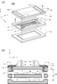
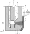
- FIG. 1 is the perspective view which looked at the 1st piezoelectric device 100 of the divided state from the base 40 side.
- B is an AA cross-sectional view of (a).
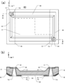
- A) is a top view of the base 40.
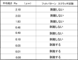
- B) is a BB sectional view of (a). It is the figure which confirmed the peeling state by the scratch test of the electrode film of arithmetic mean roughness Ra of the bottom surface roughened surface.
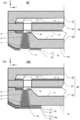
- (A) is an enlarged sectional view of the package 80.
- (B) is an enlarged cross-sectional view of the first piezoelectric device 100.
- 3 is an enlarged cross-sectional view of a second piezoelectric device 110 including a tuning fork type crystal vibrating piece 30.
- FIG. FIG. 6 is a cross-sectional view of the first piezoelectric device 100 mounted on a mounting substrate 85 and soldered.
- FIG. 1 is a schematic diagram of a first piezoelectric device 100 including a tuning fork type crystal vibrating piece 30 according to the present embodiment.
- FIG. 1A is a perspective view of the divided first piezoelectric device 100 as viewed from the base 40 side
- FIG. 1B is a cross-sectional view taken along line AA in FIG.
- the first piezoelectric device 100 includes a base 40, a crystal frame 20, and a lid 10.
- the lid 10 and the base 40 are made of a quartz material.
- the crystal frame 20 has a tuning fork type crystal vibrating piece 30 formed by etching.
- the first piezoelectric device 100 has a package 80 in which a lid 10 is bonded under the crystal frame 20 and a base 40 is bonded over the crystal frame 20 around the crystal frame 20 including the tuning fork type crystal vibrating piece 30. Is formed. That is, the lid 10 is bonded to the crystal frame 20 and the base 40 is bonded to the crystal frame 20 by a siloxane bond (Si—O—Si).
- the lid 10 has a lid-side concave portion 17 on one side of the crystal frame 20 side.
- the crystal frame 20 has a so-called tuning fork type crystal vibrating piece 30 at the center and an outer frame part 21 on the outside, and a gap 22 is formed between the tuning fork type crystal vibrating piece 30 and the outer frame part 21. Is formed.
- the tuning fork type crystal vibrating piece 30 has a base 32 and a pair of vibrating arms 31 extending from the base 32. The base 32 and the vibrating arm 31 are surrounded by the outer frame portion 21.
- the gap 22 that defines the outer shape of the tuning-fork type crystal vibrating piece 30 is formed by wet etching.
- the tuning fork type crystal vibrating piece 30 has the same thickness as the outer frame portion 21.
- the tuning-fork type crystal vibrating piece 30 includes a first excitation electrode 35 and a second excitation electrode formed on a first main surface and a second main surface,
- the first excitation electrode 35 is connected to the first extraction electrode 33 formed on the base portion 32 and the outer frame portion 21, and the second excitation electrode is connected to the second extraction electrode 34 formed on the base portion 32 and the outer frame portion 21. linked.
- a weight portion 37 is formed at the tip of the vibrating arm 31 of the crystal vibrating piece 30.
- the first extraction electrode 33, the second extraction electrode 34, the first excitation electrode 35, the second excitation electrode, and the weight portion 37 are simultaneously formed by a photolithography process. When a voltage is applied to these, the crystal vibrating piece 30 vibrates at a predetermined frequency.
- the weight portion 37 is a weight for facilitating the vibration arm 31 of the crystal vibrating piece 30 to vibrate and is provided for frequency adjustment.
- the base 40 has a base-side recess 47 on one side of the crystal frame 20 side.
- the base 40 includes a tapered surface 45 toward the outer periphery of the opposite surface on the crystal frame 20 side.
- the base 40 is formed with a through hole TH, a first connection electrode 42, a second connection electrode 42, and a first external electrode layer 50 composed of two layers, and a through hole wiring 15 is formed in the through hole TH.
- the base 40 will be described later with reference to FIG.
- the first piezoelectric device 100 is sealed by forming a package 80 by siloxane bonding, placing a sealing material 70 in the upward through-hole TH, and heating to a predetermined temperature in a vacuum reflow furnace for a certain period of time.
- the material 70 is melted and sealed.
- the sealing material 70 is formed of a kind of eutectic metal gold / germanium (Au12Ge) alloy, gold / silicon (Au3.15Si) alloy and gold / tin (Au20Sn) alloy.
- the package 80 in which the through hole TH is sealed has a second external structure composed of two layers so as to cover the first external electrode layer 50 and the sealing material 70.
- An electrode layer 50a is formed.
- the 1st piezoelectric device 100 provided with the external electrode layer which consists of four layers is formed.
- the first piezoelectric device 100 is depicted as one product. However, in actuality, hundreds of piezoelectric devices 100 are formed on a piezoelectric wafer for mass production, and the individual first piezoelectric devices 100 are formed by a dicing process. As individualized. The first external electrode layer 50 and the second external electrode layer 50a of the first piezoelectric device 100 are separated from the piezoelectric wafer by the dicing process to separate the first external electrode layer 50 and the second external electrode layer 50a. The external electrode layer 50a does not peel off from the package bottom 60. That is, the first piezoelectric device 100 with high electrical reliability is formed.
- FIG. 2A is a top view of the base 40
- FIG. 2B is a cross-sectional view taken along the line BB of FIG.
- the first base 40 is formed of a Z-cut crystal.
- the base-side recess 47 is provided on one side of the crystal frame 20 so as not to contact the tuning-fork type crystal vibrating piece 30.
- the base 40 forms a stepped portion 49 around the entire periphery of the base-side recess 47.
- the first connection electrode 42 and the second connection electrode 44 are formed in a part of the step portion 49.
- the heights of the first connection electrode 42 and the second connection electrode 44 are 200 angstroms ( ⁇ ) to 3000 angstroms ( ⁇ ), and if the step portion 49 is not provided, the outer periphery of the first base 40 and the first crystal frame This may become an obstacle when the outer frame portion 20 of the 20 is bonded to a siloxane bond (Si—O—Si).
- the step portion 49 is formed with a depth of 150 ⁇ to 2000 ⁇ .
- a through hole TH penetrating the bottom surface of the base 40 is formed in the stepped portion 49 by wet etching or the like.
- a through hole wiring 15 is provided in the through hole TH.
- a first connection electrode 42 and a second connection electrode 44 connected to the through hole TH are formed in a part of the step portion 49. The first connection electrode 42 and the second connection electrode 44 are electrically connected to the first external electrode layer 50 provided on the base 40 through the through hole wiring 15 of the through hole TH.
- the bottom portion 60 of the base 40 is provided with a tapered surface 45 toward the outer periphery of the base 40.
- the bottom 60 of the base 40 is surface-roughened and has an arithmetic average roughness Ra of 0.1 ⁇ m or more.
- a first external electrode layer 50 is formed on the bottom 60 of the base 40.
- the first connection electrode 42 and the second connection electrode 44, the through-hole wiring 15 and the first external electrode layer 50 are composed of two layers.
- the first metal layer 51 of nickel or chromium and the second metal of the gold layer are formed by sputtering or vacuum deposition. Layer 52 is formed simultaneously.
- the surface roughening of the bottom 60 of the base 40 makes the first external electrode layer 50 difficult to peel off.
- Providing the tapered surface 45 in the peripheral portion of the base 40 facilitates soldering during surface mounting, and makes it difficult to be affected by external impacts by obtaining sufficient solder fixing strength.
- the surface roughening method includes a wet etching method using hydrofluoric acid, a sand blasting method using alumina abrasive grains, a plasma etching method using carbon tetrafluoride, and an ion milling method using ionized argon.
- a sandblasting method using alumina abrasive grains was used.
- FIG. 3 is a table in which the peeled state of the electrode film having the arithmetic average roughness Ra of the surface roughening is confirmed by a scratch test.
- a diamond indenter having a certain radius of curvature is pressed against the first external electrode layer 50, the first external electrode layer 50 is scratched while increasing the load, and the first external electrode layer 50 is broken.
- the adhesion strength is obtained.
- the first external electrode layer was applied by applying the fact that the interfacial delamination occurs when the displacement stress acting on the interface exceeds the adhesion strength when scratching while pressing the diamond indenter against the first external electrode layer 50 with a constant load. The possibility of peeling of 50 was confirmed.
- arithmetic average roughness Ra was 0.1 ⁇ m or more, the first external electrode layer 50 was not peeled off, and when it was 0.05 ⁇ m or less, the first external electrode layer 50 was peeled off.
- arithmetic mean roughness Ra was measured based on JIS1994.
- FIG. 4A is a preparatory process for manufacturing the first piezoelectric device 100, and is a diagram illustrating the first external electrode layer 50 of the package 80 in which the through hole TH is sealed with the sealing material 70.
- FIG. 4A shows a state in which the lid 10, the crystal frame 20, and the base 40 are coupled and the through hole TH is sealed with the sealing material 70. Description overlapping with the base 40 described in FIG. 2 is omitted. Further, the structure around the second connection electrode 44 (not shown) is the same as the structure of the first connection electrode 42, and the description thereof will be omitted.
- the lid 80, the crystal frame 20, and the base 40 are siloxane-bonded in an atmospheric state to form a package 80.
- the package 80 is arranged so that the base 40 faces upward, and a spherical sealing material 70 of gold / germanium (Au12Ge) alloy is arranged in the through hole TH on the bottom surface side of the base 40.
- the package 80 in which the spherical sealing material 70 is arranged is conveyed in a vacuum reflow furnace at around 350 ° C.
- the air in the package 80 is exhausted from the gap between the spherical sealing material 70 and the through hole TH, and the inside of the package 80 is evacuated.
- the sealing material 70 starts to melt gradually.
- some gas is generated from the inside of the sealing material 70, but the gas is also absorbed by the vacuum reflow furnace, so that the gas does not stay in the package 80.
- the sealing material 70 is crushed using a plate jig (not shown).
- the sealing material 70 enters the through hole TH. Since the through-hole wiring 15 is formed in the through-hole TH, the melted sealing material 70 flows out along the through-hole wiring 15. That is, the through-hole wiring 15 improves wettability, and the sealing material 70 seals the through-hole TH.
- the inside of the package 80 is sealed at a predetermined degree of vacuum.
- FIG. 4B is a diagram illustrating the second external electrode layer 50a of the first piezoelectric device 100 in which the through hole TH is sealed with the sealing material 70.
- FIG. The first piezoelectric device 100 shown in FIG. 4B is in a state where the second external electrode layer 50a is formed on the package 80 in the state shown in FIG.
- the second external electrode layer 50a composed of the third metal layer 53 and the fourth metal layer 54 is deposited or sputtered so as to cover the first external electrode layer 50 and the sealing material 70. It is formed by.
- the third metal layer 53 is nickel or a nickel-chromium (Ni ⁇ Cr) alloy
- the fourth metal layer 54 is a gold layer.
- the external electrode of the first piezoelectric device 100 includes a first external electrode layer 50 and a second external electrode layer 50a, and is configured with four layers. Further, the second external electrode layer 50a covers the sealing material 70, and the sealing material 70 does not appear on the surface as an external electrode.
- the gold layer of the fourth metal layer 54 Since the gold layer of the fourth metal layer 54 appears on the surface, the gold layer of the fourth metal layer 54 is also soldered when the first piezoelectric device 100 is soldered to the mounting substrate 85 (see FIG. 6). It diffuses to 75 (FIG. 6) and the first piezoelectric device 100 is firmly fixed.
- the nickel or nickel-chromium alloy of the third metal layer 53 is a metal that easily forms an oxide film, but is oxidized by the gold layer of the fourth metal layer 54.
- the gold layer of the fourth metal layer 54 of the second external electrode layer 50a diffuses into the solder by the first soldering, but the nickel or nickel-chromium alloy of the third metal layer 53 is not present in the second external electrode. The remaining can be repeatedly soldered.
- the gold layer of the fourth metal layer 54 is already lost in the third metal layer 53, but is prevented from being oxidized because it is covered with the solder film. .
- first piezoelectric devices 100 When the plurality of first piezoelectric devices 100 are individually separated from the formed piezoelectric wafer, there is no separation between the first external electrode layer 50 and the second external electrode layer 50a and the package bottom 60. That is, since the package bottom 60 has a roughened surface, peeling is suppressed by the anchor effect. Therefore, even if the first piezoelectric device 100 is repeatedly soldered, the first external electrode layer 50 and the second external electrode layer 50a are maintained.
- FIG. 5 is an enlarged cross-sectional view of the second piezoelectric device 110 including the tuning-fork type crystal vibrating piece 30 according to the present embodiment.
- the difference between the first piezoelectric device 100 and the second piezoelectric device 110 is that four second external electrode layers 50 b are formed so as to cover the first external electrode layer 50 and the sealing material 70.
- the same members as those in the first embodiment are denoted by the same reference numerals, and differences from the first embodiment will be described.
- FIG. 5 shows a state in which the through hole TH is sealed with the sealing material 70 and then the second external electrode layer 50b is formed.
- a first metal layer 53, a fourth metal layer 54, a fifth metal layer 55, and a sixth metal layer 56 are formed so as to cover the first external electrode layer 50 and the sealing material 70.
- Two external electrode layers 50b are formed by vapor deposition or sputtering.
- the third metal layer 53 is nickel or a nickel-chromium alloy
- the fourth metal layer 54 is a gold layer
- the fifth metal layer 55 is nickel or a nickel-chromium alloy
- the sixth metal layer 56 is a gold layer. is there. That is, the external electrode of the second piezoelectric device 110 includes the first external electrode layer 50 and the second external electrode layer 50b, and is configured with six layers.
- the first metal layer 51 to the second metal layer 52 and the third metal layer 53 to the sixth metal layer 56 have the same thickness.
- the thickness of the third metal layer 53 to the sixth metal layer 56 can be reduced. That is, the time required for vapor deposition or sputtering for each layer is shortened.
- the third metal layer 53 to the sixth metal layer 56 are formed, it is possible to suppress the formation of minute protrusions called hillocks on the surface of the metal layer.
- the nickel or nickel-chromium alloy of the fifth metal layer 55 is a metal that easily forms an oxide film, but is oxidized by the gold layer of the sixth metal layer 56 before being soldered.
- the gold layer of the sixth metal layer 56 of the second external electrode layer 50b diffuses into the solder by the first soldering, but the nickel or nickel-chromium alloy of the fifth metal layer 55 is not contained in the second external electrode. The remaining can be repeatedly soldered. Further, since the thickness of the gold layer of the sixth metal layer 56 can be reduced, the amount of gold diffused into the solder is also reduced.
- the second piezoelectric device 110 is repeatedly soldered, even if the gold layer of the sixth metal layer 56 is lost, the nickel or nickel-chromium alloy of the fifth metal layer 55 is oxidized. It is prevented.
- the first external electrode layer 50, the second external electrode layer 50b, and the package bottom 60 are peeled off. Although force is applied, peeling is suppressed by the anchor effect due to surface roughening.
- FIG. 6 is a cross-sectional view of the second piezoelectric device 110 mounted on the mounting substrate 85 and soldered. Since the base 40 of the second piezoelectric device 110 has a tapered surface 45 toward the outer periphery, the contact area between the solder 75 and the mounting substrate 85 is widened, and a sufficient solder fixing strength is obtained, so that an external impact can be obtained. It becomes difficult to be affected. Further, since the tapered surface 45 is provided, it is easy to confirm soldering when the second piezoelectric device 110 is surface-mounted on the mounting substrate 85, and the number of inspection steps in the manufacturing process can be reduced.
- the tuning fork type piezoelectric vibrating piece 30 thinner than the outer frame portion, it is possible to use a flat base and lid without providing recesses in the base and lid.
- an AT vibrating piece or a surface acoustic wave (SAW) piece can be used instead of the tuning fork type piezoelectric vibrating piece 30.
- the first metal layer 51 is made of nickel or chromium, but nickel / chromium alloy, titanium or tantalum can also be used.
- the 3rd metal layer 53 and the 5th metal layer 55 used the material of nickel or nickel-chromium alloy, chromium, titanium, or tantalum can also be used.
Abstract
A piezoelectric device has excellent bonding by using solder and excellent electrical continuity by forming an external electrode layer so as to cover a sealing material after tightly sealing a through hole with a sealing material. In a piezoelectric device (100), a lid (10), a piezoelectric plate (20) which includes a piezoelectric oscillation piece having an oscillation electrode formed thereon and an extraction electrode, and a base (40) having a through hole (TH) are connected. The base is provided with: connecting electrodes (42, 44) which are connected to the extraction electrode on the piezoelectric plate side; a through hole electrode (15) which is electrically connected to the connecting electrode and is formed in the through hole; a first external electrode layer (50) which is electrically connected to the through hole electrode and is formed on the opposite surface to the piezoelectric plate; a sealing material (70) which seals the through hole electrode; and a second external electrode layer (50a) which is formed to cover the first external electrode layer (50) and the sealing material (70).
Description
本発明は、圧電振動片をパッケージ内に配置した圧電デバイスの製造方法に関する。
The present invention relates to a method for manufacturing a piezoelectric device in which a piezoelectric vibrating piece is arranged in a package.
小型の情報機器や、携帯電話、又は移動体通信機器や圧電ジャイロセンサー等において、圧電振動子や圧電発振器等の圧電デバイスが広く使用されている。情報機器又は移動体通信機器等の小型軽量化及び高周波数化に伴って、それらに用いられる圧電デバイスなども、より一層の小型化及び高周波数化への対応が求められている。
Piezoelectric devices such as piezoelectric vibrators and piezoelectric oscillators are widely used in small information devices, mobile phones, mobile communication devices, piezoelectric gyro sensors, and the like. As information devices or mobile communication devices become smaller and lighter and have higher frequencies, piezoelectric devices and the like used for these devices are also required to respond to further miniaturization and higher frequencies.
従来、圧電デバイスは、金属、ガラス又はセラミックからなるリッドとガラス又はセラミックからなるパッケージ部材とを重ね合わせて接合したパッケージ内に圧電振動片を搭載して、パッケージの底部に表面実装用の外部電極を設けている。外部電極層は、下地金属層にCr、Ni、又はTi層を形成し、表面層としてAu層又はAg層が形成されている。
Crはガラスと密着するが、表面実装時のハンダ付けに適さない金属であるため、Crと接合しハンダ付け可能な金属であるAuをCrの表面に形成している。二層膜としてCr/Au、Cr/Ni、Ni/Au、Ti/Au及びW/Auなどが用いられ、積層膜としてCr/Ni/Pd及びCr/Ni/Auなどが用いられている。このような圧電デバイスは、例えば特許文献1に記載されたものが知られている。 Conventionally, a piezoelectric device has a piezoelectric vibrating piece mounted in a package in which a lid made of metal, glass or ceramic and a package member made of glass or ceramic are overlapped and joined, and an external electrode for surface mounting at the bottom of the package Is provided. In the external electrode layer, a Cr, Ni, or Ti layer is formed on a base metal layer, and an Au layer or an Ag layer is formed as a surface layer.
Although Cr is in close contact with glass, it is a metal that is not suitable for soldering during surface mounting. Therefore, Au, which is a metal that can be soldered and bonded to Cr, is formed on the surface of Cr. Cr / Au, Cr / Ni, Ni / Au, Ti / Au, W / Au, etc. are used as the bilayer film, and Cr / Ni / Pd, Cr / Ni / Au, etc. are used as the laminated film. As such a piezoelectric device, for example, one described in Patent Document 1 is known.
このようなガラス又はセラミックパッケージを使って製造される圧電デバイスは、ウエハ単位で製造される。そして圧電ウエハから個々の圧電デバイスを切り離す際に加わる力によって、外部電極とパッケージの底部との間に剥がれが生じ、例えば、圧電デバイスを実装基板へ取り付けた際の強度が得られない。更に、ハンダ実装後の部品修正や再搭載時のハンダ密着性が不十分で、電極部の剥離に至る懸念がある。
このため、特許文献2は、パッケージの底部を粗面化しアンカー効果によって外部電極とパッケージの底部との間に剥がれが生じ難くする技術を開示している。 Piezoelectric devices manufactured using such glass or ceramic packages are manufactured on a wafer basis. The force applied when the individual piezoelectric devices are separated from the piezoelectric wafer causes peeling between the external electrode and the bottom of the package. For example, the strength when the piezoelectric device is attached to the mounting substrate cannot be obtained. Furthermore, there is a concern that the adhesiveness at the time of component correction after solder mounting or re-mounting is insufficient, leading to peeling of the electrode part.
For this reason, Patent Document 2 discloses a technique in which the bottom of the package is roughened and the peeling between the external electrode and the bottom of the package is less likely to occur due to the anchor effect.
しかしながら、いずれもパッケージのベース部分にスルーホールを形成する圧電デバイスではない。圧電デバイスの量産性を高めるため、圧電振動子を有する圧電フレームウエハに対してリッドウエハとベースウエハとを大気中で接合した後、真空又は不活性ガス中でスルーホールを封止材で封止する圧電デバイスが登場してきている。このようなスルーホールを有する圧電デバイスは、フットパターンなどと呼ばれる外部電極の一部を封止材が占めていた。封止材は金(Au)を含む合金が使われるが金(Au)自体よりも導通が悪くまた実装基板にハンダ付けされる際にも十分な接合が困難であった。
However, none is a piezoelectric device that forms a through hole in the base portion of the package. To increase the mass productivity of piezoelectric devices, a lid wafer and a base wafer are bonded to a piezoelectric frame wafer having a piezoelectric vibrator in the atmosphere, and then a through hole is sealed with a sealing material in a vacuum or an inert gas. Piezoelectric devices are appearing. In the piezoelectric device having such a through hole, a sealing material occupies a part of an external electrode called a foot pattern. As the sealing material, an alloy containing gold (Au) is used. However, conduction is worse than that of gold (Au) itself, and sufficient bonding is difficult even when soldered to a mounting board.
そこで本発明の目的は、リッドウエハと圧電振動片を備えた圧電フレームのウエハとスルーホールを有するベースのウエハとをシロキサン結合によりパッケージを形成する。その後、真空中又は不活性ガス中においてスルーホールを封止材で密封する。密封後、封止材を覆うように外部電極層を形成することで、ハンダ付けの接合が良好で導通もよい圧電デバイスを提供することである。
Therefore, an object of the present invention is to form a package by a siloxane bond between a lid wafer, a wafer of a piezoelectric frame having a piezoelectric vibrating piece, and a base wafer having a through hole. Thereafter, the through hole is sealed with a sealing material in vacuum or in an inert gas. After sealing, an external electrode layer is formed so as to cover the sealing material, thereby providing a piezoelectric device with good soldering and good conduction.
第1の観点の圧電デバイスは、リッドと、励振電極が形成された圧電振動片と励振電極から引き出された引出電極とを含む圧電プレートと、スルーホールを有するベースとが結合された圧電デバイスである。そして、ベースは、圧電プレート側で引出電極と接続される接続電極と、接続電極に導通しスルーホールに形成されたスルーホール電極と、スルーホール電極に導通し圧電プレートの反対面に形成された第1外部電極層と、スルーホール電極を封止する封止材と、第1外部電極層と封止材とを覆うように形成された第2外部電極層と、を備える。
封止材が覆れた外部電極層であるために、圧電デバイスが実装基板などにハンダ付けされる際には、第2外部電極層がしっかりとした固定と導通とを確保することができる。 A piezoelectric device according to a first aspect is a piezoelectric device in which a lid, a piezoelectric plate including a piezoelectric vibrating piece on which an excitation electrode is formed, an extraction electrode extracted from the excitation electrode, and a base having a through hole are coupled. is there. And the base was formed on the opposite surface of the piezoelectric plate connected to the lead electrode on the piezoelectric plate side, the through hole electrode formed in the through hole and connected to the connection electrode, and the through hole electrode. A first external electrode layer; a sealing material for sealing the through-hole electrode; and a second external electrode layer formed to cover the first external electrode layer and the sealing material.
Since the external electrode layer is covered with the sealing material, when the piezoelectric device is soldered to a mounting substrate or the like, the second external electrode layer can be firmly fixed and conductive.
第2の観点の圧電デバイスは、接続電極、スルーホール電極、及び第1外部電極層は第1下地層と第1上面層とからなり、接続電極、スルーホール電極、及び第1外部電極層の第1下地層は同時に形成され、接続電極、スルーホール電極、及び第1外部電極層の第1上面層も同時に形成される。
第1下地層又は第1上面層は同時に形成されるため、圧電デバイスの製造が容易である。 In the piezoelectric device of the second aspect, the connection electrode, the through-hole electrode, and the first external electrode layer include a first base layer and a first upper surface layer, and the connection electrode, the through-hole electrode, and the first external electrode layer The first underlayer is formed at the same time, and the connection electrode, the through-hole electrode, and the first upper surface layer of the first external electrode layer are also formed at the same time.
Since the first underlayer or the first upper surface layer is formed at the same time, the manufacture of the piezoelectric device is easy.
第3の観点の圧電デバイスは、ベースの圧電プレートの反対面は算術平均粗さRaが0.1μm以上になっており、その反対面に第1外部電極層が形成されている。
算術平均粗さRaが0.1μm以上では、第1外部電極層の剥離が起こらない。このため、圧電デバイスを実装基板に実装した後に圧電デバイスを取り外す必要がある場合でも、その圧電デバイスを再度実装することができる。 In the piezoelectric device of the third aspect, the opposite surface of the base piezoelectric plate has an arithmetic average roughness Ra of 0.1 μm or more, and a first external electrode layer is formed on the opposite surface.
When the arithmetic average roughness Ra is 0.1 μm or more, the first external electrode layer does not peel off. For this reason, even when it is necessary to remove the piezoelectric device after mounting the piezoelectric device on the mounting substrate, the piezoelectric device can be mounted again.
第4の観点の圧電デバイスは、第1外部電極層が形成される領域に、ベース外周に向かってテーパ面が形成されている。
テーパ面が形成されていると、圧電デバイスが実装基板にハンダ付けされた際に圧電デバイスのハンダ固着強度が十分得られる。また圧電デバイスが実装基板に実装された際にハンダ付けの確認が容易となる。 In the piezoelectric device according to the fourth aspect, a tapered surface is formed toward the outer periphery of the base in a region where the first external electrode layer is formed.
When the taper surface is formed, the solder fixing strength of the piezoelectric device can be sufficiently obtained when the piezoelectric device is soldered to the mounting substrate. In addition, when the piezoelectric device is mounted on the mounting substrate, it is easy to confirm the soldering.
第5の観点の圧電デバイスの製造方法は、リッドと、励振電極が形成された圧電振動片と励振電極から引き出された引出電極とを含む圧電プレートと、スルーホールを有するベースとが接合された圧電デバイスの製造方法である。この方法は、ベースの圧電プレート側の接続電極と接続電極に導通しスルーホールに形成されたスルーホール電極とスルーホール電極に導通し圧電プレートの反対面に形成された第1外部電極層とを形成する第1電極形成工程と、スルーホール電極を封止材で封止する封止工程と、第1外部電極層と封止材とを覆うように第2外部電極層を形成する第2電極形成工程と、を備える。
第1電極形成工程で形成されたスルーホール電極が封止材で封止された後、第2電極形成工程で封止材を覆う第2電極形成を形成する工程が行われる。このため第2外部電極層はしっかりとした固定と導通とを確保することができる。 According to a fifth method of manufacturing a piezoelectric device, a lid, a piezoelectric plate including a piezoelectric vibrating piece on which an excitation electrode is formed, and an extraction electrode extracted from the excitation electrode, and a base having a through hole are joined. It is a manufacturing method of a piezoelectric device. In this method, a connection electrode on the piezoelectric plate side of the base, a through-hole electrode formed in the through hole through the connection electrode, and a first external electrode layer formed in the opposite surface of the piezoelectric plate through the through-hole electrode are formed. A first electrode forming step to be formed, a sealing step for sealing the through-hole electrode with a sealing material, and a second electrode for forming the second external electrode layer so as to cover the first external electrode layer and the sealing material Forming step.
After the through-hole electrode formed in the first electrode forming step is sealed with a sealing material, a step of forming a second electrode forming the sealing material in the second electrode forming step is performed. Therefore, the second external electrode layer can ensure firm fixation and conduction.
第5の観点において、第6の観点の第1電極形成工程が、第1下地層を形成しその上に第1上面層を形成し、第2電極形成工程は、第2下地層を形成しその上に第2上面層を形成する。
第7の観点の圧電デバイスの製造方法は、第5の観点において、第1電極形成工程の前に、算術平均粗さRaが0.1mm以上にベースの圧電プレートの反対面を形成する粗面化工程を備える。
ベースの圧電プレートの反対面が粗面化されると、第1外部電極層の剥離が起こらない。 In the fifth aspect, the first electrode forming step of the sixth aspect forms the first underlayer and forms the first upper surface layer thereon, and the second electrode forming step forms the second underlayer. A second upper surface layer is formed thereon.
According to a seventh aspect of the method for manufacturing a piezoelectric device, in the fifth aspect, before the first electrode forming step, a rough surface that forms the opposite surface of the base piezoelectric plate with an arithmetic average roughness Ra of 0.1 mm or more. The process is equipped.
When the opposite surface of the base piezoelectric plate is roughened, the first external electrode layer does not peel off.
第8の観点の圧電デバイスの製造方法は、第5の観点において、粗面化工程の前に、第1外部電極層が形成される領域にベース外周に向かってテーパ面を形成する。
テーパ面が形成されることで、圧電デバイスが実装基板にハンダ付けされた際にハンダ固着強度が十分得られる。 In the fifth aspect, the piezoelectric device manufacturing method according to the eighth aspect forms a tapered surface toward the outer periphery of the base in the region where the first external electrode layer is formed before the roughening step.
By forming the tapered surface, a sufficient solder fixing strength can be obtained when the piezoelectric device is soldered to the mounting substrate.
本発明の圧電デバイスは、再ハンダ付け可能な表面実装型圧電デバイスであり、圧電デバイスを実装基板から取り外しが複数回可能となり、携帯情報機器などの電子機器の開発段階に於いて圧電デバイスの試用が容易になる。また、外部電極が多層膜構成になることによって一層あたりの金属膜を薄くでき、製膜時間が短くなることで製膜時の温度上昇が抑えられ、高温製膜時に発生するヒロックと呼ばれる異常突起の発生を抑制することができる。そして、ハンダ実装後の部品修正や再搭載時のハンダ密着性が得られ、外部電極とパッケージ底部60との間に剥がれ難い圧電デバイスを提供することができる。
The piezoelectric device of the present invention is a surface-mount type piezoelectric device that can be re-soldered. The piezoelectric device can be detached from the mounting substrate a plurality of times, and the piezoelectric device can be used in the development stage of electronic equipment such as portable information equipment. Becomes easier. In addition, the outer electrode has a multilayer film structure, so that the metal film per layer can be made thin, and the temperature rise during film formation can be suppressed by shortening the film formation time, and abnormal projections called hillocks that occur during high temperature film formation Can be suppressed. In addition, it is possible to provide a piezoelectric device that can obtain component adhesion after solder mounting and solder adhesion at the time of remounting, and that does not easily peel off between the external electrode and the package bottom 60.
<第1実施形態;第1圧電デバイス100の構成>
図1は、本実施例の音叉型水晶振動片30を備えた第1圧電デバイス100の概略図を示している。図1(a)は、分割した状態の第1圧電デバイス100を、ベース40側からみた斜視図であり、図1(b)は、(a)のA-A断面図である。 <First Embodiment; Configuration ofFirst Piezoelectric Device 100>
FIG. 1 is a schematic diagram of a firstpiezoelectric device 100 including a tuning fork type crystal vibrating piece 30 according to the present embodiment. FIG. 1A is a perspective view of the divided first piezoelectric device 100 as viewed from the base 40 side, and FIG. 1B is a cross-sectional view taken along line AA in FIG.
図1は、本実施例の音叉型水晶振動片30を備えた第1圧電デバイス100の概略図を示している。図1(a)は、分割した状態の第1圧電デバイス100を、ベース40側からみた斜視図であり、図1(b)は、(a)のA-A断面図である。 <First Embodiment; Configuration of
FIG. 1 is a schematic diagram of a first
図1(a)に示されるように、第1圧電デバイス100は、ベース40、水晶フレーム20及びリッド10から構成される。リッド10及びベース40は水晶材料から形成される。水晶フレーム20は、エッチングにより形成された音叉型水晶振動片30を有している。
As shown in FIG. 1A, the first piezoelectric device 100 includes a base 40, a crystal frame 20, and a lid 10. The lid 10 and the base 40 are made of a quartz material. The crystal frame 20 has a tuning fork type crystal vibrating piece 30 formed by etching.
第1圧電デバイス100は、音叉型水晶振動片30を備えた水晶フレーム20を中心に、その水晶フレーム20の下にリッド10が接合され、水晶フレーム20の上にベース40が接合されてパッケージ80が形成されている。つまり、リッド10は水晶フレーム20に、ベース40は水晶フレーム20にシロキサン結合(Si-O-Si)で接合する。リッド10は、リッド側凹部17を水晶フレーム20側の片面に有している。
The first piezoelectric device 100 has a package 80 in which a lid 10 is bonded under the crystal frame 20 and a base 40 is bonded over the crystal frame 20 around the crystal frame 20 including the tuning fork type crystal vibrating piece 30. Is formed. That is, the lid 10 is bonded to the crystal frame 20 and the base 40 is bonded to the crystal frame 20 by a siloxane bond (Si—O—Si). The lid 10 has a lid-side concave portion 17 on one side of the crystal frame 20 side.
水晶フレーム20は、その中央部にいわゆる音叉型水晶振動片30と外側に外枠部21とを有しており、音叉型水晶振動片30と外枠部21との間には空隙部22が形成されている。音叉型水晶振動片30は、基部32と基部32から伸びる一対の振動腕31とを有している。基部32及び振動腕31は外枠部21で囲まれている。音叉型水晶振動片30の外形を規定する空隙部22はウェットエッチングにより形成されている。音叉型水晶振動片30は外枠部21と同じ厚さである。
The crystal frame 20 has a so-called tuning fork type crystal vibrating piece 30 at the center and an outer frame part 21 on the outside, and a gap 22 is formed between the tuning fork type crystal vibrating piece 30 and the outer frame part 21. Is formed. The tuning fork type crystal vibrating piece 30 has a base 32 and a pair of vibrating arms 31 extending from the base 32. The base 32 and the vibrating arm 31 are surrounded by the outer frame portion 21. The gap 22 that defines the outer shape of the tuning-fork type crystal vibrating piece 30 is formed by wet etching. The tuning fork type crystal vibrating piece 30 has the same thickness as the outer frame portion 21.
図1(a)、(b)に示されるように、音叉型水晶振動片30は、第1主面及び第2主面に第1励振電極35及び第2励振電極が形成されており、第1励振電極35は、基部32及び外枠部21に形成された第1引出電極33につながっており、第2励振電極は、基部32及び外枠部21に形成された第2引出電極34につながっている。また、水晶振動片30の振動腕31の先端には、錘部37が形成されている。第1引出電極33、第2引出電極34、第1励振電極35、第2励振電極並びに錘部37は、同時にフォトリソグラフィ工程で作成される。これらに電圧が加えられると水晶振動片30は所定の周波数で振動する。錘部37は水晶振動片30の振動腕31が振動し易くなるための錘であり且つ周波数調整のために設けられる。
As shown in FIGS. 1A and 1B, the tuning-fork type crystal vibrating piece 30 includes a first excitation electrode 35 and a second excitation electrode formed on a first main surface and a second main surface, The first excitation electrode 35 is connected to the first extraction electrode 33 formed on the base portion 32 and the outer frame portion 21, and the second excitation electrode is connected to the second extraction electrode 34 formed on the base portion 32 and the outer frame portion 21. linked. A weight portion 37 is formed at the tip of the vibrating arm 31 of the crystal vibrating piece 30. The first extraction electrode 33, the second extraction electrode 34, the first excitation electrode 35, the second excitation electrode, and the weight portion 37 are simultaneously formed by a photolithography process. When a voltage is applied to these, the crystal vibrating piece 30 vibrates at a predetermined frequency. The weight portion 37 is a weight for facilitating the vibration arm 31 of the crystal vibrating piece 30 to vibrate and is provided for frequency adjustment.
ベース40は、ベース側凹部47を水晶フレーム20側の片面に有している。ベース40は、水晶フレーム20側の反対面の外周に向かってテーパ面45を備える。ベース40は、スルーホールTH及び第1接続電極42、第2接続電極42並びに2層から成る第1外部電極層50が形成され、スルーホールTHにはスルーホール配線15が形成される。ベース40については、図2を用いて後述する。
The base 40 has a base-side recess 47 on one side of the crystal frame 20 side. The base 40 includes a tapered surface 45 toward the outer periphery of the opposite surface on the crystal frame 20 side. The base 40 is formed with a through hole TH, a first connection electrode 42, a second connection electrode 42, and a first external electrode layer 50 composed of two layers, and a through hole wiring 15 is formed in the through hole TH. The base 40 will be described later with reference to FIG.
第1圧電デバイス100は、シロキサン結合によりパッケージ80を形成後、上向きになっているスルーホールTHに封止材70を配置し、真空リフロー炉で所定の温度に一定時間加熱されることで封止材70が溶かされ封止が行われる。封止材70は、共晶金属の金・ゲルマニューム(Au12Ge)合金、金・シリコン(Au3.15Si)合金及び金・スズ(Au20Sn)合金の一種から形成される。
The first piezoelectric device 100 is sealed by forming a package 80 by siloxane bonding, placing a sealing material 70 in the upward through-hole TH, and heating to a predetermined temperature in a vacuum reflow furnace for a certain period of time. The material 70 is melted and sealed. The sealing material 70 is formed of a kind of eutectic metal gold / germanium (Au12Ge) alloy, gold / silicon (Au3.15Si) alloy and gold / tin (Au20Sn) alloy.
図1(a)、(b)に示されるように、スルーホールTHが封止されたパッケージ80は、第1外部電極層50と封止材70とを覆うように2層から成る第2外部電極層50aが形成される。そして4層から成る外部電極層を備えた第1圧電デバイス100が形成される。
As shown in FIGS. 1A and 1B, the package 80 in which the through hole TH is sealed has a second external structure composed of two layers so as to cover the first external electrode layer 50 and the sealing material 70. An electrode layer 50a is formed. And the 1st piezoelectric device 100 provided with the external electrode layer which consists of four layers is formed.
図1では第1圧電デバイス100は1つの製品として描かれているが、実際には大量に生産するために圧電ウエハ上に何百と形成されており、ダイシング工程によって個々の第1圧電デバイス100として個片化される。第1圧電デバイス100の第1外部電極層50及び第2外部電極層50aは、圧電ウエハからダイシング工程によって個々の第1圧電デバイス100として切り離す際に加わる力によって第1外部電極層50及び第2外部電極層50aがパッケージ底部60から剥がれが生じることがない。すなわち、電気的信頼性の高い第1圧電デバイス100が形成される。
In FIG. 1, the first piezoelectric device 100 is depicted as one product. However, in actuality, hundreds of piezoelectric devices 100 are formed on a piezoelectric wafer for mass production, and the individual first piezoelectric devices 100 are formed by a dicing process. As individualized. The first external electrode layer 50 and the second external electrode layer 50a of the first piezoelectric device 100 are separated from the piezoelectric wafer by the dicing process to separate the first external electrode layer 50 and the second external electrode layer 50a. The external electrode layer 50a does not peel off from the package bottom 60. That is, the first piezoelectric device 100 with high electrical reliability is formed.
(ベース40の構成)
図2(a)はベース40の上面図であり、(b)は(a)のB-B断面図である。
第1ベース40はZカットの水晶で形成され、図2(a)及び(b)に示されるように、音叉型水晶振動片30に接しないようにベース側凹部47を水晶フレーム20側の片面に有している。ベース40はベース側凹部47の周囲全体に段差部49を形成する。この段差部49の一部に第1接続電極42及び第2接続電極44が形成される。第1接続電極42及び第2接続電極44の高さは、200オングストローム(Å)~3000オングストローム(Å)であり、段差部49を設けないと、第1ベース40の外周部と第1水晶フレーム20の外枠部21とがシロキサン結合(Si-O-Si)する際に障害となることがある。段差部49は150オングストローム~2000オングストロームの深さで形成される。 (Configuration of base 40)
2A is a top view of thebase 40, and FIG. 2B is a cross-sectional view taken along the line BB of FIG.
Thefirst base 40 is formed of a Z-cut crystal. As shown in FIGS. 2A and 2B, the base-side recess 47 is provided on one side of the crystal frame 20 so as not to contact the tuning-fork type crystal vibrating piece 30. Have. The base 40 forms a stepped portion 49 around the entire periphery of the base-side recess 47. The first connection electrode 42 and the second connection electrode 44 are formed in a part of the step portion 49. The heights of the first connection electrode 42 and the second connection electrode 44 are 200 angstroms (Å) to 3000 angstroms (Å), and if the step portion 49 is not provided, the outer periphery of the first base 40 and the first crystal frame This may become an obstacle when the outer frame portion 20 of the 20 is bonded to a siloxane bond (Si—O—Si). The step portion 49 is formed with a depth of 150 Å to 2000 Å.
図2(a)はベース40の上面図であり、(b)は(a)のB-B断面図である。
第1ベース40はZカットの水晶で形成され、図2(a)及び(b)に示されるように、音叉型水晶振動片30に接しないようにベース側凹部47を水晶フレーム20側の片面に有している。ベース40はベース側凹部47の周囲全体に段差部49を形成する。この段差部49の一部に第1接続電極42及び第2接続電極44が形成される。第1接続電極42及び第2接続電極44の高さは、200オングストローム(Å)~3000オングストローム(Å)であり、段差部49を設けないと、第1ベース40の外周部と第1水晶フレーム20の外枠部21とがシロキサン結合(Si-O-Si)する際に障害となることがある。段差部49は150オングストローム~2000オングストロームの深さで形成される。 (Configuration of base 40)
2A is a top view of the
The
ベース40は、ウェットエッチングなどにより段差部49にベース40の底面と貫通するスルーホールTHを形成する。スルーホールTHにはスルーホール配線15が設けられる。段差部49の一部には、スルーホールTHと接続する第1接続電極42及び第2接続電極44が形成される。そして、第1接続電極42及び第2接続電極44は、スルーホールTHのスルーホール配線15を通じてベース40に設けた第1外部電極層50に電気的に接続する。
In the base 40, a through hole TH penetrating the bottom surface of the base 40 is formed in the stepped portion 49 by wet etching or the like. A through hole wiring 15 is provided in the through hole TH. A first connection electrode 42 and a second connection electrode 44 connected to the through hole TH are formed in a part of the step portion 49. The first connection electrode 42 and the second connection electrode 44 are electrically connected to the first external electrode layer 50 provided on the base 40 through the through hole wiring 15 of the through hole TH.
またベース40の底部60には、ベース40の外周に向かってテーパ面45を備える。ベース40の底部60は、表面粗面化が施され算術平均粗さRaが0.1μm以上である。ベース40の底部60には、第1外部電極層50が形成されている。第1接続電極42及び第2接続電極44、スルーホール配線15並びに第1外部電極層50は二層からなり、スパッタリング又は真空蒸着によってニッケル又はクロムの第1金属層51と金層の第2金属層52とが同時に形成される。ベース40の底部60の表面粗面化は第1外部電極層50が剥離されにくくする。ベース40の周辺部にテーパ面45を設けることにより、表面実装時のハンダ付けが容易となり、ハンダ固着強度が十分得られることにより外部からの衝撃の影響を受けにくくなる。
Further, the bottom portion 60 of the base 40 is provided with a tapered surface 45 toward the outer periphery of the base 40. The bottom 60 of the base 40 is surface-roughened and has an arithmetic average roughness Ra of 0.1 μm or more. A first external electrode layer 50 is formed on the bottom 60 of the base 40. The first connection electrode 42 and the second connection electrode 44, the through-hole wiring 15 and the first external electrode layer 50 are composed of two layers. The first metal layer 51 of nickel or chromium and the second metal of the gold layer are formed by sputtering or vacuum deposition. Layer 52 is formed simultaneously. The surface roughening of the bottom 60 of the base 40 makes the first external electrode layer 50 difficult to peel off. Providing the tapered surface 45 in the peripheral portion of the base 40 facilitates soldering during surface mounting, and makes it difficult to be affected by external impacts by obtaining sufficient solder fixing strength.
表面粗面化の方法は、フッ酸を用いるウェットエッチング方法、アルミナ砥粒を用いたサンドブラスト方法、四フッ化炭素を用いるプラズマエッチング方法及びイオン化したアルゴンを用いるイオンミリング方法などがある。本実施例では、アルミナ砥粒を用いたサンドブラスト方法を用いた。ベース40の底部60は表面粗面化を施すことにより膜密着性が向上して膜の剥離のないパッケージが形成できる。
The surface roughening method includes a wet etching method using hydrofluoric acid, a sand blasting method using alumina abrasive grains, a plasma etching method using carbon tetrafluoride, and an ion milling method using ionized argon. In this example, a sandblasting method using alumina abrasive grains was used. By subjecting the bottom 60 of the base 40 to surface roughening, film adhesion is improved and a package without film peeling can be formed.
図3は、表面粗面化の算術平均粗さRaの電極膜をスクラッチ試験により剥離状態を確認した表である。
スクラッチ試験法は、一定の曲率半径を持つダイヤモンド圧子を第1外部電極層50に押し付け荷重を増加させながら第1外部電極層50を引っ掻き、第1外部電極層50の破壊が発生する荷重値から密着強度を求めるものである。今回の試験では、一定荷重でダイヤモンド圧子を第1外部電極層50に押しつけながら引っ掻く時に界面に作用するズレ応力が密着強度を上回った時に界面剥離が生ずることを応用して、第1外部電極層50の剥離の可否を確認した。この結果、算術平均粗さRaが0.1μm以上では、第1外部電極層50の剥離は起こらず、0.05μm以下では、第1外部電極層50の剥離は起こった。なお、算術平均粗さRaはJIS1994に基づいて測定した。 FIG. 3 is a table in which the peeled state of the electrode film having the arithmetic average roughness Ra of the surface roughening is confirmed by a scratch test.
In the scratch test method, a diamond indenter having a certain radius of curvature is pressed against the firstexternal electrode layer 50, the first external electrode layer 50 is scratched while increasing the load, and the first external electrode layer 50 is broken. The adhesion strength is obtained. In this test, the first external electrode layer was applied by applying the fact that the interfacial delamination occurs when the displacement stress acting on the interface exceeds the adhesion strength when scratching while pressing the diamond indenter against the first external electrode layer 50 with a constant load. The possibility of peeling of 50 was confirmed. As a result, when the arithmetic average roughness Ra was 0.1 μm or more, the first external electrode layer 50 was not peeled off, and when it was 0.05 μm or less, the first external electrode layer 50 was peeled off. In addition, arithmetic mean roughness Ra was measured based on JIS1994.
スクラッチ試験法は、一定の曲率半径を持つダイヤモンド圧子を第1外部電極層50に押し付け荷重を増加させながら第1外部電極層50を引っ掻き、第1外部電極層50の破壊が発生する荷重値から密着強度を求めるものである。今回の試験では、一定荷重でダイヤモンド圧子を第1外部電極層50に押しつけながら引っ掻く時に界面に作用するズレ応力が密着強度を上回った時に界面剥離が生ずることを応用して、第1外部電極層50の剥離の可否を確認した。この結果、算術平均粗さRaが0.1μm以上では、第1外部電極層50の剥離は起こらず、0.05μm以下では、第1外部電極層50の剥離は起こった。なお、算術平均粗さRaはJIS1994に基づいて測定した。 FIG. 3 is a table in which the peeled state of the electrode film having the arithmetic average roughness Ra of the surface roughening is confirmed by a scratch test.
In the scratch test method, a diamond indenter having a certain radius of curvature is pressed against the first
(第1圧電デバイス100の形成)
図4(a)は、第1圧電デバイス100を製造する準備工程であり、封止材70でスルーホールTHが封止されたパッケージ80の第1外部電極層50を説明する図である。図4(a)は、リッド10と水晶フレーム20とベース40とを結合し、封止材70でスルーホールTHを封止した状態である。図2で説明したベース40と重複する説明は省略する。また図示しない第2接続電極44の周辺の構造も第1接続電極42と同じ構造であるため説明を割愛する。 (Formation of the first piezoelectric device 100)
FIG. 4A is a preparatory process for manufacturing the firstpiezoelectric device 100, and is a diagram illustrating the first external electrode layer 50 of the package 80 in which the through hole TH is sealed with the sealing material 70. FIG. 4A shows a state in which the lid 10, the crystal frame 20, and the base 40 are coupled and the through hole TH is sealed with the sealing material 70. Description overlapping with the base 40 described in FIG. 2 is omitted. Further, the structure around the second connection electrode 44 (not shown) is the same as the structure of the first connection electrode 42, and the description thereof will be omitted.
図4(a)は、第1圧電デバイス100を製造する準備工程であり、封止材70でスルーホールTHが封止されたパッケージ80の第1外部電極層50を説明する図である。図4(a)は、リッド10と水晶フレーム20とベース40とを結合し、封止材70でスルーホールTHを封止した状態である。図2で説明したベース40と重複する説明は省略する。また図示しない第2接続電極44の周辺の構造も第1接続電極42と同じ構造であるため説明を割愛する。 (Formation of the first piezoelectric device 100)
FIG. 4A is a preparatory process for manufacturing the first
まず、大気状態で、リッド10と水晶フレーム20とベース40とはシロキサン結合されてパッケージ80が形成される。パッケージ80はベース40が上になるように配置して、ベース40の底面側のスルーホールTHに、金・ゲルマニューム(Au12Ge)合金の球状の封止材70が配置される。この球状の封止材70が配置されたパッケージ80は、350度C前後の真空リフロー炉内で搬送される。球状の封止材70とスルーホールTHとの隙間からパッケージ80内の空気が排気され、パッケージ80内が真空にされる。
First, the lid 80, the crystal frame 20, and the base 40 are siloxane-bonded in an atmospheric state to form a package 80. The package 80 is arranged so that the base 40 faces upward, and a spherical sealing material 70 of gold / germanium (Au12Ge) alloy is arranged in the through hole TH on the bottom surface side of the base 40. The package 80 in which the spherical sealing material 70 is arranged is conveyed in a vacuum reflow furnace at around 350 ° C. The air in the package 80 is exhausted from the gap between the spherical sealing material 70 and the through hole TH, and the inside of the package 80 is evacuated.
その後、封止材70が徐々に溶け始める。封止材70が溶け始めると封止材70内から多少のガスが発生するが、そのガスも真空リフロー炉により吸収されるためパッケージ80内にガスが滞留することがない。球状の封止材70は溶融しても表面張力で球状の状態を維持していることが多いため、不図示のプレート冶具を使って封止材70が押しつぶされる。これにより図4(a)に示されるように、封止材70がスルーホールTHに入り込む。スルーホールTHにスルーホール配線15が形成されているので、溶けた封止材70はスルーホール配線15に沿って流れ出す。つまりスルーホール配線15が濡れ性を向上させ、封止材70がスルーホールTHを封止する。以上のようにして、パッケージ80内が所定の真空度で封止される。
After that, the sealing material 70 starts to melt gradually. When the sealing material 70 starts to melt, some gas is generated from the inside of the sealing material 70, but the gas is also absorbed by the vacuum reflow furnace, so that the gas does not stay in the package 80. Since the spherical sealing material 70 often maintains a spherical state due to surface tension even when melted, the sealing material 70 is crushed using a plate jig (not shown). As a result, as shown in FIG. 4A, the sealing material 70 enters the through hole TH. Since the through-hole wiring 15 is formed in the through-hole TH, the melted sealing material 70 flows out along the through-hole wiring 15. That is, the through-hole wiring 15 improves wettability, and the sealing material 70 seals the through-hole TH. As described above, the inside of the package 80 is sealed at a predetermined degree of vacuum.
なお、封止材70が配置されたパッケージ80が真空リフロー炉内で搬送される場合について説明したが、真空リフロー炉を真空にした後、不活性ガスを投入してパッケージ80内が不活性ガスに満たされるようにしてもよい。
In addition, although the case where the package 80 in which the sealing material 70 is arranged is transported in the vacuum reflow furnace has been described, after the vacuum reflow furnace is evacuated, an inert gas is introduced to make the inside of the package 80 an inert gas. May be satisfied.
図4(b)は、封止材70でスルーホールTHが封止された第1圧電デバイス100の第2外部電極層50aを説明する図である。図4(b)に示される第1圧電デバイス100は、図4(a)の状態のパッケージ80に第2外部電極層50aを形成した状態である。
FIG. 4B is a diagram illustrating the second external electrode layer 50a of the first piezoelectric device 100 in which the through hole TH is sealed with the sealing material 70. FIG. The first piezoelectric device 100 shown in FIG. 4B is in a state where the second external electrode layer 50a is formed on the package 80 in the state shown in FIG.
図4(b)に示されるように、第1外部電極層50と封止材70とを覆うように第3金属層53及び第4金属層54からなる第2外部電極層50aが蒸着又はスパッタリングにより形成される。第3金属層53は、ニッケル又はニッケル・クロム(Ni・Cr)合金であり、第4金属層54は金層である。第1圧電デバイス100の外部電極は、第1外部電極層50と第2外部電極層50aとからなり4層で構成される。また、第2外部電極層50aが封止材70を覆い、封止材70が外部電極として表面に現れない。第4金属層54の金層が表面に現れているため、実装基板85(図6を参照)に第1圧電デバイス100がハンダ付けされる際にも、第4金属層54の金層がハンダ75(図6)に拡散し第1圧電デバイス100がしっかりと固定される。
As shown in FIG. 4B, the second external electrode layer 50a composed of the third metal layer 53 and the fourth metal layer 54 is deposited or sputtered so as to cover the first external electrode layer 50 and the sealing material 70. It is formed by. The third metal layer 53 is nickel or a nickel-chromium (Ni · Cr) alloy, and the fourth metal layer 54 is a gold layer. The external electrode of the first piezoelectric device 100 includes a first external electrode layer 50 and a second external electrode layer 50a, and is configured with four layers. Further, the second external electrode layer 50a covers the sealing material 70, and the sealing material 70 does not appear on the surface as an external electrode. Since the gold layer of the fourth metal layer 54 appears on the surface, the gold layer of the fourth metal layer 54 is also soldered when the first piezoelectric device 100 is soldered to the mounting substrate 85 (see FIG. 6). It diffuses to 75 (FIG. 6) and the first piezoelectric device 100 is firmly fixed.
第3金属層53のニッケル又はニッケル・クロム合金は酸化被膜を形成しやすい金属であるが、第4金属層54の金層により酸化防止されている。第2外部電極層50aの第4金属層54の金層は、最初のハンダ付けによりハンダ中に拡散してしまうが、第3金属層53のニッケル又はニッケル・クロム合金は第2外部電極中に残り、繰り返しハンダ付けが可能である。第1圧電デバイス100が繰り返しハンダ付けされる際には、第3金属層53はすでに第4金属層54の金層が失われているが、ハンダ被膜に覆われているため酸化防止されている。
The nickel or nickel-chromium alloy of the third metal layer 53 is a metal that easily forms an oxide film, but is oxidized by the gold layer of the fourth metal layer 54. The gold layer of the fourth metal layer 54 of the second external electrode layer 50a diffuses into the solder by the first soldering, but the nickel or nickel-chromium alloy of the third metal layer 53 is not present in the second external electrode. The remaining can be repeatedly soldered. When the first piezoelectric device 100 is repeatedly soldered, the gold layer of the fourth metal layer 54 is already lost in the third metal layer 53, but is prevented from being oxidized because it is covered with the solder film. .
第1圧電デバイス100が複数形成された圧電ウエハから個々に切り離される際に、第1外部電極層50及び第2外部電極層50aとパッケージ底部60との間で剥離することがない。つまりパッケージ底部60は表面が粗面化されているためアンカー効果により剥離が抑制されている。このため第1圧電デバイス100は繰り返しハンダ付けされても、第1外部電極層50及び第2外部電極層50aが維持される。
When the plurality of first piezoelectric devices 100 are individually separated from the formed piezoelectric wafer, there is no separation between the first external electrode layer 50 and the second external electrode layer 50a and the package bottom 60. That is, since the package bottom 60 has a roughened surface, peeling is suppressed by the anchor effect. Therefore, even if the first piezoelectric device 100 is repeatedly soldered, the first external electrode layer 50 and the second external electrode layer 50a are maintained.
<第2実施形態;第2圧電デバイス110の構成>
図5は、本実施例の音叉型水晶振動片30を備えた第2圧電デバイス110の拡大断面図である。第1圧電デバイス100と第2圧電デバイス110との違いは、第1外部電極層50及び封止材70を覆うように4層の第2外部電極層50bが形成された点である。以下、第1実施形態と同じ部材には同じ符号を付し、第1実施形態と異なる点を説明する。 <Second Embodiment; Configuration ofSecond Piezoelectric Device 110>
FIG. 5 is an enlarged cross-sectional view of the secondpiezoelectric device 110 including the tuning-fork type crystal vibrating piece 30 according to the present embodiment. The difference between the first piezoelectric device 100 and the second piezoelectric device 110 is that four second external electrode layers 50 b are formed so as to cover the first external electrode layer 50 and the sealing material 70. Hereinafter, the same members as those in the first embodiment are denoted by the same reference numerals, and differences from the first embodiment will be described.
図5は、本実施例の音叉型水晶振動片30を備えた第2圧電デバイス110の拡大断面図である。第1圧電デバイス100と第2圧電デバイス110との違いは、第1外部電極層50及び封止材70を覆うように4層の第2外部電極層50bが形成された点である。以下、第1実施形態と同じ部材には同じ符号を付し、第1実施形態と異なる点を説明する。 <Second Embodiment; Configuration of
FIG. 5 is an enlarged cross-sectional view of the second
図5は、封止材70でスルーホールTHが封止され、その後第2外部電極層50bが形成した状態である。
図5に示されるように、第1外部電極層50と封止材70とを覆うように第3金属層53及び第4金属層54並びに第5金属層55及び第6金属層56からなる第2外部電極層50bが蒸着又はスパッタリングにより形成される。第3金属層53はニッケル又はニッケル・クロム合金であり、第4金属層54は金層であり、第5金属層55はニッケル又はニッケル・クロム合金であり、第6金属層56は金層である。すなわち第2圧電デバイス110の外部電極は、第1外部電極層50と第2外部電極層50bとからなり6層で構成される。 FIG. 5 shows a state in which the through hole TH is sealed with the sealingmaterial 70 and then the second external electrode layer 50b is formed.
As shown in FIG. 5, afirst metal layer 53, a fourth metal layer 54, a fifth metal layer 55, and a sixth metal layer 56 are formed so as to cover the first external electrode layer 50 and the sealing material 70. Two external electrode layers 50b are formed by vapor deposition or sputtering. The third metal layer 53 is nickel or a nickel-chromium alloy, the fourth metal layer 54 is a gold layer, the fifth metal layer 55 is nickel or a nickel-chromium alloy, and the sixth metal layer 56 is a gold layer. is there. That is, the external electrode of the second piezoelectric device 110 includes the first external electrode layer 50 and the second external electrode layer 50b, and is configured with six layers.
図5に示されるように、第1外部電極層50と封止材70とを覆うように第3金属層53及び第4金属層54並びに第5金属層55及び第6金属層56からなる第2外部電極層50bが蒸着又はスパッタリングにより形成される。第3金属層53はニッケル又はニッケル・クロム合金であり、第4金属層54は金層であり、第5金属層55はニッケル又はニッケル・クロム合金であり、第6金属層56は金層である。すなわち第2圧電デバイス110の外部電極は、第1外部電極層50と第2外部電極層50bとからなり6層で構成される。 FIG. 5 shows a state in which the through hole TH is sealed with the sealing
As shown in FIG. 5, a
なお、図4(b)と図5では、第1金属層51から第2金属層52と、第3金属層53から第6金属層56との厚さが同じような厚さで描かれているが、第3金属層53から第6金属層56の厚さを薄くすることができる。すなわち、各層に対する蒸着又はスパッタリングにかかる時間は短縮される。さらに第3金属層53から第6金属層56の成膜時に、金属層の表面にヒロックと呼ばれる微細な突起が形成されることも抑制できる。
In FIG. 4B and FIG. 5, the first metal layer 51 to the second metal layer 52 and the third metal layer 53 to the sixth metal layer 56 have the same thickness. However, the thickness of the third metal layer 53 to the sixth metal layer 56 can be reduced. That is, the time required for vapor deposition or sputtering for each layer is shortened. Furthermore, when the third metal layer 53 to the sixth metal layer 56 are formed, it is possible to suppress the formation of minute protrusions called hillocks on the surface of the metal layer.
第5金属層55のニッケル又はニッケル・クロム合金は酸化被膜を形成しやすい金属であるが、ハンダ付けされる前は第6金属層56の金層により酸化防止されている。第2外部電極層50bの第6金属層56の金層は、最初のハンダ付けによりハンダ中に拡散してしまうが、第5金属層55のニッケル又はニッケル・クロム合金は第2外部電極中に残り、繰り返しハンダ付けが可能である。また、第6金属層56の金層の厚さも薄くできるので、ハンダ中に拡散する金の量も少なくなる。第2圧電デバイス110が繰り返しハンダ付けされる際には、第6金属層56の金層が失われてもハンダ被膜に覆われているため第5金属層55のニッケル又はニッケル・クロム合金は酸化防止されている。
The nickel or nickel-chromium alloy of the fifth metal layer 55 is a metal that easily forms an oxide film, but is oxidized by the gold layer of the sixth metal layer 56 before being soldered. The gold layer of the sixth metal layer 56 of the second external electrode layer 50b diffuses into the solder by the first soldering, but the nickel or nickel-chromium alloy of the fifth metal layer 55 is not contained in the second external electrode. The remaining can be repeatedly soldered. Further, since the thickness of the gold layer of the sixth metal layer 56 can be reduced, the amount of gold diffused into the solder is also reduced. When the second piezoelectric device 110 is repeatedly soldered, even if the gold layer of the sixth metal layer 56 is lost, the nickel or nickel-chromium alloy of the fifth metal layer 55 is oxidized. It is prevented.
仮に、第2圧電デバイス110が繰り返しハンダ付けされて、第5金属層55のニッケル又はニッケル・クロム合金及び第6金属層56の金層が失われても、第3金属層53のニッケル又はニッケル・クロム合金及び第4金属層54の金層が存在しているため、更なるハンダ付けが可能である。
Even if the second piezoelectric device 110 is repeatedly soldered and the nickel or nickel-chromium alloy of the fifth metal layer 55 and the gold layer of the sixth metal layer 56 are lost, the nickel or nickel of the third metal layer 53 is lost. -Since the gold layer of the chromium alloy and the fourth metal layer 54 exists, further soldering is possible.
また、第2圧電デバイス110が複数形成された圧電ウエハから個々の第2圧電デバイス110を切り離す際に、第1外部電極層50及び第2外部電極層50bとパッケージ底部60との間に剥離の力が加わるが、表面粗面化によるアンカー効果により剥離が抑制される。
Further, when the individual second piezoelectric devices 110 are separated from the piezoelectric wafer on which a plurality of the second piezoelectric devices 110 are formed, the first external electrode layer 50, the second external electrode layer 50b, and the package bottom 60 are peeled off. Although force is applied, peeling is suppressed by the anchor effect due to surface roughening.
図6は、第2圧電デバイス110を実装基板85に搭載しハンダ付けを行った断面図である。第2圧電デバイス110のベース40は、外周に向かってテーパ面45を備えているため、ハンダ75と実装基板85との密着面積が広くなり、ハンダ固着強度が十分得られることにより外部からの衝撃の影響を受けにくくなる。また、テーパ面45があるために、第2圧電デバイス110が実装基板85に表面実装された際にハンダ付けの確認が容易となり、製造工程での検査工数を軽減できる。
FIG. 6 is a cross-sectional view of the second piezoelectric device 110 mounted on the mounting substrate 85 and soldered. Since the base 40 of the second piezoelectric device 110 has a tapered surface 45 toward the outer periphery, the contact area between the solder 75 and the mounting substrate 85 is widened, and a sufficient solder fixing strength is obtained, so that an external impact can be obtained. It becomes difficult to be affected. Further, since the tapered surface 45 is provided, it is easy to confirm soldering when the second piezoelectric device 110 is surface-mounted on the mounting substrate 85, and the number of inspection steps in the manufacturing process can be reduced.
以上、実施形態について詳細に説明したが、当業者に明らかなように、本発明はその技術的範囲内において上記各実施例に様々な変更・変形を加えて実施することができる。たとえば、音叉型圧電振動片30を外枠部より薄くすることにより、ベース及びリッドに凹部を設けることなく、平板状のベース及びリッドを用いることができる。また、音叉型圧電振動片30に代えAT振動片、弾性表面波(SAW)片を用いることができる。
As described above, the embodiments have been described in detail. However, as will be apparent to those skilled in the art, the present invention can be implemented by adding various changes and modifications to the above embodiments within the technical scope thereof. For example, by making the tuning fork type piezoelectric vibrating piece 30 thinner than the outer frame portion, it is possible to use a flat base and lid without providing recesses in the base and lid. Further, an AT vibrating piece or a surface acoustic wave (SAW) piece can be used instead of the tuning fork type piezoelectric vibrating piece 30.
さらに、上記実施形態では、第1金属層51はニッケル又はクロムの材料を使用したが、ニッケル・クロム合金、チタン又はタンタルも使用できる。また、第3金属層53及び第5金属層55はニッケル又はニッケル・クロム合金の材料を使用したが、クロム、チタン又はタンタルも使用できる。
Furthermore, in the above embodiment, the first metal layer 51 is made of nickel or chromium, but nickel / chromium alloy, titanium or tantalum can also be used. Moreover, although the 3rd metal layer 53 and the 5th metal layer 55 used the material of nickel or nickel-chromium alloy, chromium, titanium, or tantalum can also be used.
10 …… リッド
15 …… スルーホール配線
17 …… リッド側凹部
20 …… 水晶フレーム
21 …… 外枠部
22 …… 空隙部
30 …… 音叉型水晶振動片
31 …… 振動腕
32 …… 基部
33 …… 第1引出電極,34 …… 第2引出電極
35,36 …… 励振電極
37,38 …… 錘部
40 …… ベース
42 …… 第1接続電極、44 …… 第2接続電極
45 …… テーパ面
47 …… ベース側凹部
49 …… 段差部
50 …… 第1外部電極、50a、50b …… 第2外部電極
51 …… 第1金属層、52 …… 第2金属層
53 …… 第3金属層、54 …… 第4金属層
55 …… 第5金属層、56 …… 第6金属層
60 …… 表面粗面化
70 …… 封止材
75 …… ハンダ
80 …… パッケージ
85 …… 実装基板
100 …… 第1圧電デバイス、
110 …… 第2圧電デバイス
TH …… スルーホール
10...Lid 15... Through-hole wiring 17... Lid side recess 20... Crystal frame 21... Outer frame portion 22 .. Gaps 30 .. Tuning fork type crystal vibrating piece 31. First extraction electrode 34 34 Second extraction electrode 35 36 36 Excitation electrodes 37 38 38 Weight 40 Base 42 First connection electrode 44 Second connection electrode 45 Tapered surface 47 ... Base-side recess 49 ... Step 50 ... First external electrode, 50a, 50b ... Second external electrode 51 ... First metal layer, 52 ... Second metal layer 53 ... Third Metal layer 54 ... Fourth metal layer 55 ... Fifth metal layer 56 ... Sixth metal layer 60 ... Surface roughening 70 ... Sealing material 75 ... Solder 80 ... Package 85 ... Mounting Substrate 100 ... the first piezoelectric device,
110 …… Second piezoelectric device TH …… Through hole
15 …… スルーホール配線
17 …… リッド側凹部
20 …… 水晶フレーム
21 …… 外枠部
22 …… 空隙部
30 …… 音叉型水晶振動片
31 …… 振動腕
32 …… 基部
33 …… 第1引出電極,34 …… 第2引出電極
35,36 …… 励振電極
37,38 …… 錘部
40 …… ベース
42 …… 第1接続電極、44 …… 第2接続電極
45 …… テーパ面
47 …… ベース側凹部
49 …… 段差部
50 …… 第1外部電極、50a、50b …… 第2外部電極
51 …… 第1金属層、52 …… 第2金属層
53 …… 第3金属層、54 …… 第4金属層
55 …… 第5金属層、56 …… 第6金属層
60 …… 表面粗面化
70 …… 封止材
75 …… ハンダ
80 …… パッケージ
85 …… 実装基板
100 …… 第1圧電デバイス、
110 …… 第2圧電デバイス
TH …… スルーホール
10...
110 …… Second piezoelectric device TH …… Through hole
Claims (9)
- リッドと、励振電極が形成された圧電振動片と前記励振電極から引き出された引出電極とを含む圧電プレートと、スルーホールを有するベースとが接合された圧電デバイスにおいて、
前記ベースは、
前記圧電プレート側で前記引出電極と接続される接続電極と、
前記接続電極に導通し前記スルーホールに形成されたスルーホール電極と、
前記スルーホール電極に導通し、前記圧電プレートの反対面に形成された第1外部電極層と、
前記スルーホール電極を封止する封止材と、
前記第1外部電極層と前記封止材とを覆うように形成された第2外部電極層と、
を備えることを特徴とする圧電デバイス。 In a piezoelectric device in which a lid, a piezoelectric plate including a piezoelectric vibrating piece on which an excitation electrode is formed, an extraction electrode extracted from the excitation electrode, and a base having a through hole are joined,
The base is
A connection electrode connected to the extraction electrode on the piezoelectric plate side;
A through-hole electrode formed in the through-hole in conduction with the connection electrode;
A first external electrode layer electrically connected to the through-hole electrode and formed on the opposite surface of the piezoelectric plate;
A sealing material for sealing the through-hole electrode;
A second external electrode layer formed to cover the first external electrode layer and the sealing material;
A piezoelectric device comprising: - 前記接続電極、前記スルーホール電極、及び前記第1外部電極層は第1下地層と第1上面層とからなり、前記接続電極、前記スルーホール電極、及び前記第1外部電極層の第1下地層は同時に形成され、前記接続電極、前記スルーホール電極、及び前記第1外部電極層の第1上面層も同時に形成されることを特徴とする請求項1に記載の圧電デバイス。 The connection electrode, the through-hole electrode, and the first external electrode layer include a first base layer and a first upper surface layer, and a first lower layer of the connection electrode, the through-hole electrode, and the first external electrode layer. The piezoelectric device according to claim 1, wherein a ground layer is formed at the same time, and the connection electrode, the through-hole electrode, and a first upper surface layer of the first external electrode layer are formed at the same time.
- 前記ベースの前記圧電プレートの反対面は算術平均粗さRaが0.1μm以上になっており、その反対面に前記第1外部電極層が形成されていることを特徴とする請求項1に記載の圧電デバイス。 The arithmetic surface roughness Ra of the opposite surface of the piezoelectric plate of the base is 0.1 μm or more, and the first external electrode layer is formed on the opposite surface. Piezoelectric device.
- 前記第1外部電極層が形成される領域に、前記ベース外周に向かってテーパ面が形成されていることを特徴とする請求項1から請求項3のいずれか一項に記載の圧電デバイス。 The piezoelectric device according to any one of claims 1 to 3, wherein a tapered surface is formed toward an outer periphery of the base in a region where the first external electrode layer is formed.
- 前記圧電振動片は、AT振動片、弾性表面波片又は音叉型水晶振動片であることを特徴とする請求項1ないし請求項4のいずれか一項に記載の圧電デバイス。 5. The piezoelectric device according to claim 1, wherein the piezoelectric vibrating piece is an AT vibrating piece, a surface acoustic wave piece, or a tuning fork type quartz vibrating piece.
- リッドと、励振電極が形成された圧電振動片と前記励振電極から引き出された引出電極とを含む圧電プレートと、スルーホールを有するベースとが接合された圧電デバイスの製造方法において、
前記ベースの圧電プレート側の接続電極と、前記接続電極に導通し前記スルーホールに形成されたスルーホール電極と、前記スルーホール電極に導通し前記圧電プレートの反対面に形成された第1外部電極層とを形成する第1電極形成工程と、
前記スルーホール電極を封止材で封止する封止工程と、
前記第1外部電極層と前記封止材とを覆うように第2外部電極層を形成する第2電極形成工程と、
を備えることを特徴とする圧電デバイスの製造方法。 In a method of manufacturing a piezoelectric device in which a lid, a piezoelectric plate including a piezoelectric vibrating piece on which an excitation electrode is formed, an extraction electrode extracted from the excitation electrode, and a base having a through hole are joined,
A connection electrode on the piezoelectric plate side of the base, a through-hole electrode formed in the through-hole and connected to the connection electrode, and a first external electrode formed on the opposite surface of the piezoelectric plate and connected to the through-hole electrode A first electrode forming step of forming a layer;
A sealing step of sealing the through-hole electrode with a sealing material;
A second electrode forming step of forming a second external electrode layer so as to cover the first external electrode layer and the sealing material;
A method for manufacturing a piezoelectric device comprising: - 前記第1電極形成工程は、第1下地層を形成しその上に第1上面層を形成し、前記第2電極形成工程は、第2下地層を形成しその上に第2上面層を形成することを特徴とする請求項6に記載の圧電デバイスの製造方法。 In the first electrode forming step, a first underlayer is formed and a first upper surface layer is formed thereon, and in the second electrode forming step, a second underlayer is formed and a second upper surface layer is formed thereon. A method of manufacturing a piezoelectric device according to claim 6.
- 前記第1電極形成工程の前に、算術平均粗さRaが0.1mm以上に前記ベースの前記圧電プレートの反対面を形成する粗面化工程を備えることを特徴とする請求項6又は請求項7に記載の圧電デバイスの製造方法。 7. The roughening step of forming the opposite surface of the piezoelectric plate of the base so that the arithmetic average roughness Ra is 0.1 mm or more is provided before the first electrode forming step. A method for manufacturing the piezoelectric device according to claim 7.
- 前記粗面化工程の前に、前記第1外部電極層が形成される領域に、前記ベース外周に向かってテーパ面を形成することを特徴とする請求項6から請求項8のいずれか一項に記載の圧電デバイスの製造方法。 The taper surface is formed in the area | region in which the said 1st external electrode layer is formed before the said roughening process toward the said base outer periphery, The any one of Claims 6-8 characterized by the above-mentioned. A method for manufacturing a piezoelectric device according to claim 1.
Priority Applications (3)
| Application Number | Priority Date | Filing Date | Title |
|---|---|---|---|
| US13/120,256 US8610337B2 (en) | 2008-09-29 | 2009-09-24 | Piezoelectric device and method for manufacturing same |
| CN2009801320324A CN102124648A (en) | 2008-09-29 | 2009-09-24 | Piezoelectric device and method for manufacturing same |
| EP09815879A EP2343802A4 (en) | 2008-09-29 | 2009-09-24 | Piezoelectric device and method for manufacturing same |
Applications Claiming Priority (2)
| Application Number | Priority Date | Filing Date | Title |
|---|---|---|---|
| JP2008-251180 | 2008-09-29 | ||
| JP2008251180A JP4809410B2 (en) | 2008-09-29 | 2008-09-29 | Piezoelectric device and manufacturing method thereof |
Publications (1)
| Publication Number | Publication Date |
|---|---|
| WO2010035457A1 true WO2010035457A1 (en) | 2010-04-01 |
Family
ID=42059470
Family Applications (1)
| Application Number | Title | Priority Date | Filing Date |
|---|---|---|---|
| PCT/JP2009/004789 WO2010035457A1 (en) | 2008-09-29 | 2009-09-24 | Piezoelectric device and method for manufacturing same |
Country Status (6)
| Country | Link |
|---|---|
| US (1) | US8610337B2 (en) |
| EP (1) | EP2343802A4 (en) |
| JP (1) | JP4809410B2 (en) |
| CN (1) | CN102124648A (en) |
| TW (1) | TW201014156A (en) |
| WO (1) | WO2010035457A1 (en) |
Cited By (2)
| Publication number | Priority date | Publication date | Assignee | Title |
|---|---|---|---|---|
| US20130029451A1 (en) * | 2011-07-25 | 2013-01-31 | Yu-Lun Chueh | Method for making a solar cell |
| JPWO2016111038A1 (en) * | 2015-01-08 | 2017-09-07 | 株式会社村田製作所 | Piezoelectric vibration component and manufacturing method thereof |
Families Citing this family (15)
| Publication number | Priority date | Publication date | Assignee | Title |
|---|---|---|---|---|
| JP4865002B2 (en) * | 2009-04-15 | 2012-02-01 | 日本電波工業株式会社 | Quartz sensor and sensing device |
| WO2011136070A1 (en) * | 2010-04-27 | 2011-11-03 | 京セラ株式会社 | Surface acoustic wave device and method for manufacturing same |
| CN103828395B (en) * | 2011-09-30 | 2017-05-17 | 株式会社村田制作所 | Ultrasonic sensor |
| JP5930526B2 (en) * | 2012-02-20 | 2016-06-08 | 日本電波工業株式会社 | Piezoelectric vibration element and piezoelectric device |
| JP5972598B2 (en) * | 2012-02-22 | 2016-08-17 | 日本電波工業株式会社 | Piezoelectric device and method for manufacturing piezoelectric device |
| WO2013128496A1 (en) * | 2012-03-02 | 2013-09-06 | 富士通株式会社 | Crystal resonator, and production method therefor |
| JP5980530B2 (en) * | 2012-03-15 | 2016-08-31 | 日本電波工業株式会社 | Piezoelectric device and method for manufacturing piezoelectric device |
| KR101443015B1 (en) * | 2012-08-17 | 2014-09-22 | 엔지케이 인슐레이터 엘티디 | Composite substrate, surface acoustic wave device, and method for manufacturing composite substrate |
| JP2014197731A (en) * | 2013-03-29 | 2014-10-16 | セイコーエプソン株式会社 | Oscillation device, oscillation device manufacturing method, electronic apparatus and mobile object |
| KR20140118792A (en) | 2013-03-29 | 2014-10-08 | 세이코 엡슨 가부시키가이샤 | Vibrating element, vibrator, oscillator, electronic apparatus, sensor, and moving object |
| JP6135296B2 (en) * | 2013-05-20 | 2017-05-31 | 富士通株式会社 | Package structure and method for bonding package structure to substrate |
| JP6371518B2 (en) * | 2013-12-17 | 2018-08-08 | 太陽誘電株式会社 | Piezoelectric thin film resonator, method for manufacturing the same, filter, and duplexer |
| CN105874707B (en) * | 2014-01-06 | 2019-03-22 | 株式会社大真空 | The joint construction of Piezodectric vibration device and Piezodectric vibration device and circuit substrate |
| WO2016174789A1 (en) * | 2015-04-27 | 2016-11-03 | 株式会社村田製作所 | Resonator and resonance device |
| WO2018222706A1 (en) * | 2017-05-30 | 2018-12-06 | Metis Design Corporation | Electrical via providing electrode pair access on a single side of a device |
Citations (8)
| Publication number | Priority date | Publication date | Assignee | Title |
|---|---|---|---|---|
| JPH1022773A (en) * | 1996-07-03 | 1998-01-23 | Matsushita Electric Ind Co Ltd | Vibrator and manufacture therefor |
| JPH10126205A (en) * | 1996-10-23 | 1998-05-15 | Matsushita Electric Ind Co Ltd | Electronic component and its manufacture |
| JP2006180169A (en) * | 2004-12-22 | 2006-07-06 | Kyocera Kinseki Corp | Manufacturing method of vibrator package |
| JP2006197278A (en) | 2005-01-14 | 2006-07-27 | Seiko Instruments Inc | Surface mounting piezoelectric vibrator, oscillator and electronic apparatus |
| JP2007129327A (en) * | 2005-11-01 | 2007-05-24 | Seiko Instruments Inc | Piezoelectric vibrator and oscillator provided with the same, radio clock, and electronic apparatus |
| JP2007197278A (en) | 2006-01-27 | 2007-08-09 | Mitsui Chemicals Inc | Inorganic oxide ultrafine particle and method for producing the same |
| JP2008147895A (en) * | 2006-12-08 | 2008-06-26 | Epson Toyocom Corp | Crystal oscillator and its fabricating method |
| JP2008211543A (en) * | 2007-02-27 | 2008-09-11 | Epson Toyocom Corp | Crystal resonator and method of manufacturing crystal resonator |
Family Cites Families (10)
| Publication number | Priority date | Publication date | Assignee | Title |
|---|---|---|---|---|
| JPH0559951U (en) * | 1992-01-09 | 1993-08-06 | 株式会社村田製作所 | Piezoelectric parts |
| TW569424B (en) * | 2000-03-17 | 2004-01-01 | Matsushita Electric Ind Co Ltd | Module with embedded electric elements and the manufacturing method thereof |
| JP2002319838A (en) * | 2001-02-19 | 2002-10-31 | Seiko Epson Corp | Piezoelectric device and its package |
| JP3736395B2 (en) * | 2001-07-12 | 2006-01-18 | 株式会社村田製作所 | Piezoelectric element and method for manufacturing piezoelectric element |
| CN101189921A (en) * | 2005-06-01 | 2008-05-28 | 松下电器产业株式会社 | Circuit base plate and its making method and electronic component using the same |
| JP5007522B2 (en) * | 2006-05-01 | 2012-08-22 | セイコーエプソン株式会社 | Piezoelectric vibrator and manufacturing method thereof |
| JP4647677B2 (en) * | 2008-08-11 | 2011-03-09 | 日本電波工業株式会社 | Piezoelectric device |
| JP2010141293A (en) * | 2008-11-14 | 2010-06-24 | Seiko Epson Corp | Semiconductor device and method for manufacturing the same |
| JP4763769B2 (en) * | 2008-12-03 | 2011-08-31 | 日本電波工業株式会社 | Method for manufacturing piezoelectric device |
| JP4988799B2 (en) * | 2009-09-16 | 2012-08-01 | 日本電波工業株式会社 | Piezoelectric vibration device and method for manufacturing piezoelectric vibration device |
-
2008
- 2008-09-29 JP JP2008251180A patent/JP4809410B2/en not_active Expired - Fee Related
-
2009
- 2009-08-17 TW TW98127547A patent/TW201014156A/en unknown
- 2009-09-24 US US13/120,256 patent/US8610337B2/en not_active Expired - Fee Related
- 2009-09-24 WO PCT/JP2009/004789 patent/WO2010035457A1/en active Application Filing
- 2009-09-24 CN CN2009801320324A patent/CN102124648A/en active Pending
- 2009-09-24 EP EP09815879A patent/EP2343802A4/en not_active Withdrawn
Patent Citations (8)
| Publication number | Priority date | Publication date | Assignee | Title |
|---|---|---|---|---|
| JPH1022773A (en) * | 1996-07-03 | 1998-01-23 | Matsushita Electric Ind Co Ltd | Vibrator and manufacture therefor |
| JPH10126205A (en) * | 1996-10-23 | 1998-05-15 | Matsushita Electric Ind Co Ltd | Electronic component and its manufacture |
| JP2006180169A (en) * | 2004-12-22 | 2006-07-06 | Kyocera Kinseki Corp | Manufacturing method of vibrator package |
| JP2006197278A (en) | 2005-01-14 | 2006-07-27 | Seiko Instruments Inc | Surface mounting piezoelectric vibrator, oscillator and electronic apparatus |
| JP2007129327A (en) * | 2005-11-01 | 2007-05-24 | Seiko Instruments Inc | Piezoelectric vibrator and oscillator provided with the same, radio clock, and electronic apparatus |
| JP2007197278A (en) | 2006-01-27 | 2007-08-09 | Mitsui Chemicals Inc | Inorganic oxide ultrafine particle and method for producing the same |
| JP2008147895A (en) * | 2006-12-08 | 2008-06-26 | Epson Toyocom Corp | Crystal oscillator and its fabricating method |
| JP2008211543A (en) * | 2007-02-27 | 2008-09-11 | Epson Toyocom Corp | Crystal resonator and method of manufacturing crystal resonator |
Non-Patent Citations (2)
| Title |
|---|
| JIS, 1994 |
| See also references of EP2343802A4 * |
Cited By (2)
| Publication number | Priority date | Publication date | Assignee | Title |
|---|---|---|---|---|
| US20130029451A1 (en) * | 2011-07-25 | 2013-01-31 | Yu-Lun Chueh | Method for making a solar cell |
| JPWO2016111038A1 (en) * | 2015-01-08 | 2017-09-07 | 株式会社村田製作所 | Piezoelectric vibration component and manufacturing method thereof |
Also Published As
| Publication number | Publication date |
|---|---|
| CN102124648A (en) | 2011-07-13 |
| JP2010087573A (en) | 2010-04-15 |
| US20110309720A1 (en) | 2011-12-22 |
| EP2343802A1 (en) | 2011-07-13 |
| EP2343802A4 (en) | 2012-10-17 |
| JP4809410B2 (en) | 2011-11-09 |
| US8610337B2 (en) | 2013-12-17 |
| TW201014156A (en) | 2010-04-01 |
Similar Documents
| Publication | Publication Date | Title |
|---|---|---|
| JP4809410B2 (en) | Piezoelectric device and manufacturing method thereof | |
| JP5119866B2 (en) | Quartz device and sealing method thereof | |
| JP4221756B2 (en) | Piezoelectric oscillator and manufacturing method thereof | |
| JP6247006B2 (en) | Electronic device, oscillator, and method of manufacturing electronic device | |
| JP5538974B2 (en) | Electronic device package manufacturing method and electronic device package | |
| US8261427B2 (en) | Methods for manufacturing crystal devices | |
| JP2004129223A (en) | Piezoelectric component and manufacturing method thereof | |
| WO2001067600A1 (en) | Crystal vibration device | |
| US8319404B2 (en) | Surface-mountable quartz-crystal devices and methods for manufacturing same | |
| JP2009171080A (en) | Crystal device and manufacturing method for crystal device | |
| JP2010246001A (en) | Electronic component and method of manufacturing the same | |
| US8341814B2 (en) | Methods for manufacturing piezoelectric devices | |
| JP2000232332A (en) | Surface mounted piezoelectric resonator | |
| JP2001068511A (en) | Method of mounting electronic device element and manufacture of surface acoustic wave device | |
| JP5155352B2 (en) | Piezoelectric device | |
| JP6383138B2 (en) | Electronic devices | |
| JP6230286B2 (en) | Electronic device and method for manufacturing electronic device | |
| JP2013031133A (en) | Piezoelectric vibration device | |
| JP2003318692A (en) | Piezoelectric device | |
| JP2010245266A (en) | Electronic component and method of manufacturing the same | |
| JP2007184810A (en) | Method for manufacturing piezoelectric vibrator | |
| JP2013045880A (en) | Manufacturing method of electronic device | |
| WO2021095294A1 (en) | Piezoelectric vibrator and method for manufacturing same | |
| JP2010177984A (en) | Piezoelectric vibrator and piezoelectric device | |
| JP2011091685A (en) | Piezoelectric device |
Legal Events
| Date | Code | Title | Description |
|---|---|---|---|
| WWE | Wipo information: entry into national phase |
Ref document number: 200980132032.4 Country of ref document: CN |
|
| 121 | Ep: the epo has been informed by wipo that ep was designated in this application |
Ref document number: 09815879 Country of ref document: EP Kind code of ref document: A1 |
|
| WWE | Wipo information: entry into national phase |
Ref document number: 13120256 Country of ref document: US |
|
| WWE | Wipo information: entry into national phase |
Ref document number: 2009815879 Country of ref document: EP |
|
| NENP | Non-entry into the national phase |
Ref country code: DE |