WO2010032713A1 - 集積型薄膜太陽電池およびその製造方法 - Google Patents
集積型薄膜太陽電池およびその製造方法 Download PDFInfo
- Publication number
- WO2010032713A1 WO2010032713A1 PCT/JP2009/066043 JP2009066043W WO2010032713A1 WO 2010032713 A1 WO2010032713 A1 WO 2010032713A1 JP 2009066043 W JP2009066043 W JP 2009066043W WO 2010032713 A1 WO2010032713 A1 WO 2010032713A1
- Authority
- WO
- WIPO (PCT)
- Prior art keywords
- groove
- thin film
- photoelectric conversion
- string
- electrode layer
- Prior art date
Links
- 239000010409 thin film Substances 0.000 title claims abstract description 118
- 238000004519 manufacturing process Methods 0.000 title claims description 16
- 238000006243 chemical reaction Methods 0.000 claims abstract description 118
- 238000000926 separation method Methods 0.000 claims abstract description 90
- 239000000758 substrate Substances 0.000 claims abstract description 58
- 238000011144 upstream manufacturing Methods 0.000 claims description 97
- 239000010408 film Substances 0.000 claims description 39
- 238000002955 isolation Methods 0.000 claims description 27
- 238000000034 method Methods 0.000 claims description 22
- 230000001678 irradiating effect Effects 0.000 claims description 10
- 238000010030 laminating Methods 0.000 claims description 8
- 230000000149 penetrating effect Effects 0.000 claims description 2
- 239000010410 layer Substances 0.000 description 204
- 239000004065 semiconductor Substances 0.000 description 35
- 230000015572 biosynthetic process Effects 0.000 description 19
- 229910052751 metal Inorganic materials 0.000 description 16
- 239000002184 metal Substances 0.000 description 16
- 229910021424 microcrystalline silicon Inorganic materials 0.000 description 12
- 229910021417 amorphous silicon Inorganic materials 0.000 description 11
- 239000000463 material Substances 0.000 description 10
- 239000003566 sealing material Substances 0.000 description 9
- 229910006404 SnO 2 Inorganic materials 0.000 description 8
- 229910052782 aluminium Inorganic materials 0.000 description 7
- 239000012790 adhesive layer Substances 0.000 description 6
- 230000002093 peripheral effect Effects 0.000 description 6
- XAGFODPZIPBFFR-UHFFFAOYSA-N aluminium Chemical compound [Al] XAGFODPZIPBFFR-UHFFFAOYSA-N 0.000 description 5
- 229910052709 silver Inorganic materials 0.000 description 5
- XUIMIQQOPSSXEZ-UHFFFAOYSA-N Silicon Chemical compound [Si] XUIMIQQOPSSXEZ-UHFFFAOYSA-N 0.000 description 4
- 238000005219 brazing Methods 0.000 description 4
- 239000012535 impurity Substances 0.000 description 4
- 229910052710 silicon Inorganic materials 0.000 description 4
- 239000010703 silicon Substances 0.000 description 4
- RYGMFSIKBFXOCR-UHFFFAOYSA-N Copper Chemical compound [Cu] RYGMFSIKBFXOCR-UHFFFAOYSA-N 0.000 description 3
- BQCADISMDOOEFD-UHFFFAOYSA-N Silver Chemical compound [Ag] BQCADISMDOOEFD-UHFFFAOYSA-N 0.000 description 3
- 239000004020 conductor Substances 0.000 description 3
- 239000005038 ethylene vinyl acetate Substances 0.000 description 3
- 229920001200 poly(ethylene-vinyl acetate) Polymers 0.000 description 3
- 230000011218 segmentation Effects 0.000 description 3
- 239000004332 silver Substances 0.000 description 3
- 229920002799 BoPET Polymers 0.000 description 2
- 150000001875 compounds Chemical class 0.000 description 2
- 229910021419 crystalline silicon Inorganic materials 0.000 description 2
- 230000007423 decrease Effects 0.000 description 2
- 239000000203 mixture Substances 0.000 description 2
- 229920005989 resin Polymers 0.000 description 2
- 239000011347 resin Substances 0.000 description 2
- 238000004544 sputter deposition Methods 0.000 description 2
- 238000007740 vapor deposition Methods 0.000 description 2
- ZOXJGFHDIHLPTG-UHFFFAOYSA-N Boron Chemical compound [B] ZOXJGFHDIHLPTG-UHFFFAOYSA-N 0.000 description 1
- OKTJSMMVPCPJKN-UHFFFAOYSA-N Carbon Chemical compound [C] OKTJSMMVPCPJKN-UHFFFAOYSA-N 0.000 description 1
- OAICVXFJPJFONN-UHFFFAOYSA-N Phosphorus Chemical compound [P] OAICVXFJPJFONN-UHFFFAOYSA-N 0.000 description 1
- 239000004642 Polyimide Substances 0.000 description 1
- 229910000577 Silicon-germanium Inorganic materials 0.000 description 1
- LEVVHYCKPQWKOP-UHFFFAOYSA-N [Si].[Ge] Chemical compound [Si].[Ge] LEVVHYCKPQWKOP-UHFFFAOYSA-N 0.000 description 1
- 229910052796 boron Inorganic materials 0.000 description 1
- 229910052799 carbon Inorganic materials 0.000 description 1
- 238000007796 conventional method Methods 0.000 description 1
- 239000010949 copper Substances 0.000 description 1
- 239000013078 crystal Substances 0.000 description 1
- 230000000694 effects Effects 0.000 description 1
- 238000000605 extraction Methods 0.000 description 1
- 229910052733 gallium Inorganic materials 0.000 description 1
- 229910052732 germanium Inorganic materials 0.000 description 1
- GNPVGFCGXDBREM-UHFFFAOYSA-N germanium atom Chemical compound [Ge] GNPVGFCGXDBREM-UHFFFAOYSA-N 0.000 description 1
- 239000011521 glass Substances 0.000 description 1
- 229910052738 indium Inorganic materials 0.000 description 1
- 238000000059 patterning Methods 0.000 description 1
- 229910052698 phosphorus Inorganic materials 0.000 description 1
- 239000011574 phosphorus Substances 0.000 description 1
- 238000005268 plasma chemical vapour deposition Methods 0.000 description 1
- 238000007747 plating Methods 0.000 description 1
- 229920001721 polyimide Polymers 0.000 description 1
- 238000010248 power generation Methods 0.000 description 1
- 238000007789 sealing Methods 0.000 description 1
- HBMJWWWQQXIZIP-UHFFFAOYSA-N silicon carbide Chemical compound [Si+]#[C-] HBMJWWWQQXIZIP-UHFFFAOYSA-N 0.000 description 1
- 229910010271 silicon carbide Inorganic materials 0.000 description 1
- 229920002050 silicone resin Polymers 0.000 description 1
- 229910000679 solder Inorganic materials 0.000 description 1
- XLYOFNOQVPJJNP-UHFFFAOYSA-N water Substances O XLYOFNOQVPJJNP-UHFFFAOYSA-N 0.000 description 1
Images


Classifications
-
- H01L31/0463—
-
- Y—GENERAL TAGGING OF NEW TECHNOLOGICAL DEVELOPMENTS; GENERAL TAGGING OF CROSS-SECTIONAL TECHNOLOGIES SPANNING OVER SEVERAL SECTIONS OF THE IPC; TECHNICAL SUBJECTS COVERED BY FORMER USPC CROSS-REFERENCE ART COLLECTIONS [XRACs] AND DIGESTS
- Y02—TECHNOLOGIES OR APPLICATIONS FOR MITIGATION OR ADAPTATION AGAINST CLIMATE CHANGE
- Y02E—REDUCTION OF GREENHOUSE GAS [GHG] EMISSIONS, RELATED TO ENERGY GENERATION, TRANSMISSION OR DISTRIBUTION
- Y02E10/00—Energy generation through renewable energy sources
- Y02E10/50—Photovoltaic [PV] energy
Definitions
- the present invention relates to an integrated thin film solar cell and a manufacturing method thereof.
- FIG. 2 of Patent Document 1 shows an integrated thin film solar cell (hereinafter simply referred to as a solar cell) having a string (battery row) in which a plurality of thin film photoelectric conversion elements are electrically connected in series. Is disclosed).
- a thin film photoelectric conversion element is formed by sequentially laminating a transparent electrode layer, a photoelectric conversion layer, and a metal electrode layer on the surface of a light-transmitting insulating substrate.
- the thin film photoelectric conversion elements on both sides in the series connection direction are parallel connection elements connected to the thin film photoelectric conversion elements adjacent in the direction orthogonal to the series connection direction, and a plurality of strings are formed by these parallel connection elements.
- a current collecting electrode made of a metal wire is electrically joined to the metal electrode layer of each parallel connection element via a brazing material, and a large current is generated by the metal electrode layer and the current collecting electrode. May be configured to be removable.
- the output of the entire string (the entire solar cell) is reduced if there is even one leak location in any of the thin film photoelectric conversion elements (cells) in the string. Therefore, by dividing the string into a plurality, the output of the entire solar cell does not decrease even if the output of the string in which the cell leak portion exists decreases.
- a string separation groove (lighting opening groove) having a cross-sectional shape shown in FIG.
- the string separation groove includes a first groove from which the transparent electrode layer has been removed and a second groove from which the photoelectric conversion layer and the metal electrode layer have been removed.
- the transparent electrode layer When the thin film photoelectric conversion element is removed with a light beam, the transparent electrode layer The groove width of the second groove is made wider than the groove width of the first groove so that the metal electrode layer is not short-circuited.
- This string separation groove is formed as follows.
- a YAG fundamental wave light beam capable of removing the transparent electrode layer, the photoelectric conversion layer, and the metal electrode layer at once is irradiated from the back surface (outer surface) side of the translucent insulating substrate, and penetrates from the transparent electrode layer to the metal electrode layer.
- a first groove is formed.
- the YAG fundamental wave light beam whose intensity is adjusted so that only the photoelectric conversion layer and the metal electrode layer can be removed is irradiated from the back side of the translucent insulating substrate to the region including the first groove on the inner side. Two grooves are formed.
- the string separation groove of this solar cell is formed by moving in a series connection direction while irradiating a YAG fundamental wave light beam having different intensities toward a light-transmitting insulating substrate.
- the parallel connection elements on both sides for connecting the strings in parallel are not divided, the ON / OFF of the light beam is controlled with high accuracy so that the other thin film photoelectric conversion elements between them are surely divided.
- a portion that is not divided by the light beam is covered with a mask.
- the method of ON / OFF control of the light beam is simpler as a process than the method of using a mask.
- the start and end points of the light beam are determined by ON / OFF control of the light beam irradiation while moving the beam irradiation means in the serial connection direction by the moving mechanism. Therefore, it is necessary to perform ON / OFF control of the light beam with high accuracy at a predetermined position using a precise moving mechanism capable of detecting the position of the light beam with high accuracy. Therefore, in this case, there is a demerit that the formation cost of the string separation groove increases.
- An object of the present invention is to provide an integrated thin film solar cell in which a plurality of strings are connected in parallel by forming a string separation groove by a simple and low-cost method and a method for manufacturing the same.
- a plurality of strings having a plurality of thin film photoelectric conversion elements formed on a translucent insulating substrate and electrically connected in series to each other are provided, and the thin film photoelectric conversion element includes the translucent insulating substrate.
- the translucent first electrode layer laminated on top, the photoelectric conversion layer laminated on the first electrode layer, and the second electrode layer laminated on the photoelectric conversion layer, and the strings are the same.
- a plurality of string separation grooves extending in the series connection direction are arranged in parallel on the translucent insulating substrate in a direction orthogonal to the series connection direction, and the string separation grooves remove the first electrode layer.
- an integrated thin-film solar cell in which the remaining portions are connected in parallel and extend in a direction orthogonal to the series connection direction, and a plurality of strings are electrically connected in parallel by the parallel connection element.
- a string dividing step of forming a plurality of strings by removing a predetermined portion of the string with a light beam and forming a string separation groove extending in a series connection direction, and the string forming step before dividing includes a translucent insulating substrate Forming a laminated film by laminating the first electrode layer, the photoelectric conversion layer, and the second electrode layer in this order on the surface of the substrate, and removing the second electrode layer and the photoelectric conversion layer in the laminated film in a series connection direction Forming a plurality of thin film photoelectric conversion elements by forming a plurality of element isolation grooves extending in a direction orthogonal to the string separation grooves, wherein the string isolation grooves are formed by removing the first electrode layer.
- the first groove is orthogonal to the series connection direction. Any thin film photoelectric conversion element that extends in the direction to be connected is partially removed by a light beam so that a string separation groove is formed only in a part of the thin film photoelectric conversion element.
- a method of manufacturing an integrated thin film solar cell that forms strings arranged in parallel and parallel connection elements that electrically connect a plurality of strings in parallel.
- an arbitrary thin film photoelectric conversion element adjacent in a direction orthogonal to the series connection direction is a parallel connection element in which a part is removed by a string separation groove and the remaining part is connected in parallel, and a plurality of strings Are formed by separating other thin film photoelectric conversion elements adjacent in the same direction by string separation grooves.
- the string separation groove only needs to be formed so as to remove a part of the parallel connection element that connects a plurality of strings in parallel, that is, the parallel connection element must not be removed at all. Therefore, the allowable range of formation of the end portion of the string separation groove is widened.
- the string separation groove by a simple method of controlling the movement of the light beam with a certain degree of accuracy without performing high-precision ON / OFF control of the light beam when forming the string separation groove, a plurality of It is possible to obtain an integrated thin film solar cell in which the strings are connected in parallel.
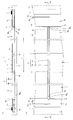
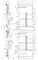
- FIG. 1 is a plan view showing Embodiment 1 of the integrated thin film solar cell of the present invention.
- 2 (a) is a cross-sectional view taken along the line II of FIG. 1
- FIG. 2 (b) is a side view of the integrated thin film solar cell of FIG. 1 viewed from the series connection direction
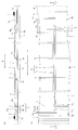
- FIG. FIG. 2 is a sectional view taken along line II-II in FIG. 3A is a cross-sectional view taken along the line III-III in FIG. 1
- FIG. 3B is a plan view showing the vicinity of the string separation groove of the integrated thin film solar cell in FIG. 4A is a partial cross-sectional view in the series connection direction in the vicinity of the string dividing groove of the integrated thin film solar cell of the second embodiment
- FIG. 4B is a string of the integrated thin film solar cell of the second embodiment.
- FIG. 4 is a partial plan view near a separation groove.
- FIG. 5A is a partial cross-sectional view in the series connection direction in the vicinity of the string dividing groove of the integrated thin film solar cell of the third embodiment, and
- FIG. 5B is a string of the integrated thin film solar cell of the third embodiment.
- FIG. 4 is a partial plan view near a separation groove.
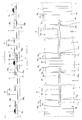
- FIG. 6 is a plan view showing Embodiment 4 of the integrated thin film solar cell of the present invention.
- FIG. 7 is a plan view showing Embodiment 5 of the integrated thin film solar cell of the present invention.
- FIG. 8A is a partial cross-sectional view in the series connection direction in the vicinity of the string dividing groove of the integrated thin film solar cell of the fifth embodiment
- FIG. 8B is a string of the integrated thin film solar cell of the fifth embodiment
- FIG. 4 is a partial plan view near a separation groove
- FIG. 9A is a partial cross-sectional view in the series connection direction in the vicinity of the string dividing groove of the integrated thin film solar cell of the sixth embodiment
- FIG. 9B is a string of the integrated thin film solar cell of the sixth embodiment.
- FIG. 4 is a partial plan view near a separation groove.
- Embodiments of the integrated thin film solar cell of the present invention will be described in detail with reference to the drawings.
- the embodiment is an example of the present invention, and the present invention is not limited to the embodiment.
- FIG. 1 is a plan view showing Embodiment 1 of the integrated thin film solar cell of the present invention.
- 2 (a) is a cross-sectional view taken along the line II of FIG. 1
- FIG. 2 (b) is a side view of the integrated thin film solar cell of FIG. 1 as viewed from the series connection direction.
- Is a cross-sectional view taken along the line II-II in FIG. 3A is a cross-sectional view taken along the line III-III of FIG. 1
- FIG. 3B is a plan view showing the vicinity of the string separation groove of the integrated thin film solar cell of FIG. 1 to 3
- an arrow E indicates a direction in which a current flows (current direction).
- upstream or downstream means upstream or downstream in the current direction.
- an arrow A indicates a serial connection direction, which means a direction in which a plurality of thin film photoelectric conversion elements connected in series are arranged.
- an arrow B indicates a direction orthogonal to the series connection direction.
- This integrated thin-film solar cell includes a rectangular translucent insulating substrate 1, a string S formed on the insulating substrate 1, and a plurality of thin-film photoelectric conversion elements 5 electrically connected in series with each other, and a string One first current collecting electrode 6 and one second current electrode which are electrically joined to the second electrode layers 4 of the thin film photoelectric conversion elements 5a and 5b on both sides of the serial connection direction A in S via a brazing material. And a current collecting electrode 7.
- the thin film photoelectric conversion element 5 is formed by laminating a transparent first electrode layer 2, a photoelectric conversion layer 3, and a second electrode layer 4 in this order on an insulating substrate 1.
- the “integrated thin film solar cell” may be abbreviated as “solar cell” as described above, and the “thin film photoelectric conversion element” may be referred to as “cell”.
- a plurality of strings S are arranged in the direction B perpendicular to the series connection direction with a plurality of (in this case, five) string separation grooves 8 extending in the series connection direction A on the same insulating substrate 1. (In this case, 6 pieces) are arranged in parallel and a plurality of strings S are connected in parallel.
- the string S is an element formed by removing the second electrode layer 4 and the photoelectric conversion layer 3 between two adjacent cells (thin film photoelectric conversion elements) 5.
- a separation groove 9 is provided.
- the element isolation groove 9 has an arrow B so as to electrically isolate the second electrode 4 and the photoelectric conversion layer 3 of one cell 5 from the second electrode 4 and the photoelectric conversion layer 3 of another adjacent cell 5. It extends in the direction.
- the groove width (in the direction of arrow A) of the element isolation groove 9 is preferably about 30 to 80 ⁇ m.
- the first electrode layer 2 of one cell 5 extends such that one end (the downstream end in the current direction E) extends across the element isolation groove 9 to a region of another adjacent cell 5.
- the electrode separation line 10 is electrically insulated from the adjacent 1st electrode layer 2 which has the part 2a.
- one end of the second electrode layer 4 of one cell 5 (upstream end portion in the current direction E) is connected to the first electrode of the adjacent cell 5 via the series conductive portion 4 a penetrating the photoelectric conversion layer 3.
- the layer 2 is electrically connected to the extending portion 2a.
- the conductive portion 4a can be integrally formed of the same material in the same process as the second electrode layer 4.
- the cells 5a and 5b to which the first and second current collecting electrodes 6 and 7 are joined are connected as shown in FIGS. 1 and 2B.
- the string separation groove 8 does not completely divide the two adjacent strings S. That is, the cells 5a and 5b at both ends in the direction of arrow A extend long in the direction of arrow B. Therefore, both ends of all the strings S are respectively connected to the first and second current collecting electrodes 6 via the common second electrode layer 4. , 7 are electrically connected in parallel. That is, the cells 5a and 5b at both ends are parallel elements that electrically connect a plurality of strings S in parallel.
- the string separation groove 8 is formed by removing the first groove 8a formed by removing the first electrode layer 2, and removing the photoelectric conversion layer 3 and the second electrode layer 4 with a width wider than the width of the first groove 8a.
- the second groove 8b The string separation groove 8 prevents the first electrode layer 2 and the second electrode layer 4 of each cell from being short-circuited.
- the groove width (arrow B direction) of the first groove 8a is preferably about 10 to 1000 ⁇ m
- the groove width (arrow B direction) of the second groove 8b is preferably about 20 to 1500 ⁇ m.
- arbitrary cells extending in the direction B orthogonal to the series connection direction A that is, the first and second current collecting electrodes 6 and 7 are provided.
- the two cells 5a and 5b joined may be partially removed by the string separation groove 8 and the remaining portions may be connected integrally.
- the end 8a 1 of the first groove 8a on the upstream side in the current direction E is upstream of the first electrode layer 2 of the cell 5 adjacent to the downstream side of the cell 5a as the upstream parallel element. Accordingly, the first electrode layers 2 of the plurality of cells 5 (in the B direction) adjacent to the cells 5a are completely insulated and separated by the first grooves 8a.
- the end 8a 1 of the first groove 8a since the end 8a 1 of the first groove 8a is disposed in the region of the element isolation groove 9 adjacent to the cell 5a, a part of the first electrode layer 2 of the cell 5a is removed. Will be.
- the position of the end 8a 1 of the first groove 8a is shifted downstream to the region of the electrode separation line 10 that insulates and separates the first electrode layer 2 of the cell 5 adjacent to the first electrode layer 2 of the cell 5a. be able to.
- the end 8b 2 of the second groove 8b on the downstream side in the current direction E is disposed on the downstream side of the second electrode layer 4 of the cell 5 adjacent to the upstream side of the cell 5b as the downstream parallel element. Accordingly, the second electrode layer 4 and the photoelectric conversion layer 3 of the plurality of cells 5 (B direction) adjacent to the cell 5b are completely insulated and separated by the second groove 8b.
- the end 8b 2 of the second groove 8b since the end 8b 2 of the second groove 8b is located in the vicinity of the element isolation groove 9 of the cell 5b, a part of the second electrode layer 4 and the photoelectric conversion layer 3 of the cell 5b is removed. Will be. In FIG.
- symbol Pa 1 represents a position where the upstream end 8a 1 of the first groove 8a is allowed to be formed in the upstream cell 5a
- symbol Pb 1 represents the second groove in the upstream cell 5a. indicates the position at which formation of the upstream-side end portion 8b 1 of 8b is allowed
- the code Pa 2 represents a position where the formation of the downstream end portion 8a 2 of the first groove 8a is allowed downstream cell 5b
- reference numeral Pb 2 is This represents a position where the downstream end 8b 2 of the second groove 8b is allowed to be formed in the downstream cell 5b.
- the end 8b 1 of the second groove 8b disposed on the upstream side in the current direction E may or may not be removed even if a part of the cell 5a (second electrode layer 4 and photoelectric conversion layer 3) is removed.
- it is not removed in the first embodiment, and is located in the region of the element isolation trench 9 adjacent to the cell 5a. That is, the end 8b 1 of the second groove 8b may be disposed within a range from the region of the cell 5 adjacent to the downstream side of the cell 5a to a position where a predetermined dimension enters the cell 5a.
- the fundamental wave of the YAG laser is used as the light beam used for forming the first groove 8a
- the first electrode layer 2 not only the first electrode layer 2 but also the photoelectric conversion layer 3 and the second electrode layer 4 are removed, so that the second groove 8b
- the position of the end of the first groove 8a coincides with at least the end of the first groove 8a, and preferably surrounds the end of the first groove 8a.
- the end portion 8a 2 of the first groove 8a arranged on the downstream side in the current direction E may or may not be removed even if a part of the cell 5b (first electrode layer 4) is removed. However, it is not removed and is located in the vicinity of the element isolation groove 9 of the cell 5 adjacent to the cell 5b. That is, the end portion 8a 2 of the first groove 8a may be disposed within a range from a region of the cell 5 adjacent to the upstream side of the cell 5b to a position where a predetermined dimension enters the cell 5b side.
- the plurality of cells 5 in the direction of the arrow B adjacent to the upstream cell 5a have their first electrode layers 2 insulated and separated. Therefore, even if one of the cells 5 leaks, the other cells 5 are not affected.
- the plurality of cells 5 adjacent to the downstream cell 5b are connected by a part of the first electrode layer 2, but the second electrode layer 4 and the photoelectric conversion layer 3 are insulated and separated. Therefore, even if one of the cells 5 leaks, the other cells 5 are not affected.
- the first electrode layer 2 of the plurality of cells 5 adjacent to the upstream cell 5a is separated at least by the first groove 8a, and the downstream cell 5b is separated by the second groove 8b.
- the allowable range of formation of the first groove 8a and the second groove 8b that is, the range in which both ends of the first groove 8a and the second groove 8b can be formed is expanded.
- the string separation groove 8 is formed by a simple method of controlling the movement of the light beam with a certain degree of accuracy without performing high-precision ON / OFF control of the light beam when forming the string separation groove 8.
- An integrated thin film solar cell in which a plurality of strings S are connected in parallel can be obtained.
- the movement control and ON / OFF control of the light beam in the direction of arrow A when forming the first groove 8a and the second groove 8b will be described in detail later.
- the length of the upstream cell 5a is 5 to 15 mm
- the length of the downstream cell 5b is 3 to 5 mm
- the length of the other cells 5 is 5 to 15 mm
- the first and first 2 When the thickness of the current collecting electrodes 6 and 7 is 1 to 2 mm and the width of the element isolation groove 9 is 30 to 80 ⁇ m, the allowable formation range La of the upstream end 8a 1 of the first groove 8a is 0 to
- the allowable range Lb of the downstream end 8b 2 of the second groove 8b can be about 0 to 2 mm.
- the formation allowable position Pa 1 of the upstream end 8a 1 of the first groove 8a is a position where the formation allowable position Pb 1 exceeding this position can be prevented from sufficiently reaching the joint location of the first current collecting electrode 6.
- the formation allowable position Pb 2 of the downstream end portion 8b 2 of the second groove 8b is a position that does not reach the junction of the second current collecting electrode 7 sufficiently.
- the cell 5b on the second collector electrode 7 side has a narrow width in the series connection direction A, and therefore does not substantially contribute to power generation. Therefore, the second electrode 4 of the cell 5b is used as a lead electrode for the first electrode 2 of the adjacent cell 5.
- the plurality of strings S are formed on the inner side of the outer peripheral end face (end face of the four sides) of the translucent insulating substrate 1. That is, the outer peripheral region on the surface of the insulating substrate 1 is a non-conductive surface region 12 in which the first electrode layer 2, the photoelectric conversion layer 3, and the second electrode layer 4 are not formed, and the width thereof is the output voltage of the solar cell.
- the dimension range is set according to
- Translucent insulating substrate and first electrode layer As the translucent insulating substrate 1, a glass substrate having heat resistance and translucency in the subsequent film forming process, a resin substrate such as polyimide, and the like can be used.
- the first electrode layer 2 is made of a transparent conductive film, and is preferably made of a transparent conductive film made of a material containing ZnO or SnO 2 .
- the material containing SnO 2 may be SnO 2 itself or a mixture of SnO 2 and another oxide (for example, ITO which is a mixture of SnO 2 and In 2 O 3 ).
- each semiconductor layer forming the photoelectric conversion layer 3 is not particularly limited, for example, made of silicon-based semiconductor, CIS (CuInSe 2) compound semiconductor, CIGS (Cu (In, Ga ) Se 2) compound semiconductor or the like.
- silicon-based semiconductor means a semiconductor (silicon carbide, silicon germanium, or the like) in which carbon, germanium, or other impurities are added to amorphous silicon, microcrystalline silicon, amorphous or microcrystalline silicon.
- microcrystalline silicon means silicon in a mixed phase state of crystalline silicon having a small crystal grain size (about several tens to thousands of thousands) and amorphous silicon. Microcrystalline silicon is formed, for example, when a crystalline silicon thin film is manufactured at a low temperature using a non-equilibrium process such as a plasma CVD method.
- the photoelectric conversion layer 3 is formed by laminating a p-type semiconductor layer, an i-type semiconductor layer, and an n-type semiconductor layer in order from the first electrode 2 side. Note that the i-type semiconductor layer may be omitted.
- the p-type semiconductor layer is doped with p-type impurity atoms such as boron and aluminum, and the n-type semiconductor layer is doped with n-type impurity atoms such as phosphorus.
- the i-type semiconductor layer may be a completely non-doped semiconductor layer, or may be a weak p-type or weak n-type semiconductor layer having a small amount of impurities and sufficiently equipped with a photoelectric conversion function.
- amorphous layer and “microcrystalline layer” mean amorphous and microcrystalline semiconductor layers, respectively.
- the photoelectric conversion layer 3 may be a tandem type in which a plurality of pin structures are stacked. For example, an a-Si: Hp layer, an a-Si: Hi layer, and an a-Si: Hn layer are formed on the first electrode 2.
- the upper semiconductor layer may be sequentially stacked, and the lower semiconductor layer may be formed by stacking a ⁇ c-Si: Hp layer, a ⁇ c-Si: Hi layer, and a ⁇ c-Si: Hn layer in this order on the upper semiconductor layer.
- the pin structure may be a photoelectric conversion layer 3 having a three-layer structure including an upper semiconductor layer, a middle semiconductor layer, and a lower semiconductor layer.
- amorphous silicon a-Si
- lower semiconductor layers are used.
- ⁇ c-Si microcrystalline silicon
- the combination of the material and laminated structure of the photoelectric conversion layer 3 is not particularly limited.
- the semiconductor layer located on the light incident side of the thin-film solar cell is the upper semiconductor layer, and the semiconductor layer located on the side opposite to the light incident side is the lower semiconductor layer.
- a straight line written in the photoelectric conversion layer 3 in (a) to (c) represents a boundary between the upper semiconductor layer and the lower semiconductor layer.
- the configuration and material of the second electrode layer 4 are not particularly limited, but in one example, the second electrode 4 has a stacked structure in which a transparent conductive film and a metal film are stacked on the photoelectric conversion layer.
- the transparent conductive film is made of ZnO, ITO, SnO 2 or the like.
- the metal film is made of a metal such as silver or aluminum.
- the second electrode layer 4 may be made of only a metal film such as Ag or Al.
- the transparent conductive film such as ZnO, ITO or SnO 2 is disposed on the photoelectric conversion layer 3 side, the second electrode layer 4 is absorbed by the photoelectric conversion layer 3.
- the reflectance which reflects the light which did not exist in the back electrode layer 4 improves, and it is preferable at the point which can obtain the thin film solar cell of high conversion efficiency.
- a back surface sealing material is laminated on the translucent insulating substrate 1 via an adhesive layer so as to completely cover the string S and the nonconductive surface region 8.
- an adhesive layer for example, a sealing resin sheet made of ethylene-vinyl acetate copolymer (EVA) can be used.
- EVA ethylene-vinyl acetate copolymer
- the back surface sealing material for example, a laminated film in which an aluminum film is sandwiched between PET films can be used.
- the adhesive layer and the back surface sealing material are previously formed with small holes for leading the leading ends of the lead wires 13 connected to the current collecting electrodes to the outside.
- a terminal box having an output line and a terminal electrically connected to each take-out line 13 is attached on the back surface sealing material.
- a frame for example, made of aluminum is attached to the outer peripheral portion of the solar cell sealed with the back surface sealing material and the adhesive layer.
- This integrated thin film solar cell includes a pre-division string forming step for forming a pre-division string in which a plurality of thin film photoelectric conversion elements are electrically connected in series to each other on the surface of the translucent insulating substrate 1, and a predetermined string for the pre-division string.
- the string separating groove 8 By forming the string separating groove 8 extending in the serial connection direction by removing the portion with a light beam, the portion can be manufactured by a manufacturing method including a string dividing step of forming a plurality of strings S.
- the string forming step before division includes a film forming step of forming a laminated film by laminating the first electrode layer, the photoelectric conversion layer, and the second electrode layer in this order on the surface of the translucent insulating substrate 1, and a second step in the laminated film. Forming a plurality of thin film photoelectric conversion elements by removing the electrode layer and the photoelectric conversion layer and forming a plurality of element isolation grooves 9 extending in a direction orthogonal to the series connection direction (arrow B direction).
- a transparent conductive film having a film thickness of 600 to 1000 nm is formed on the entire surface of the translucent insulating substrate 1 by CVD, sputtering, vapor deposition, or the like, and the transparent conductive film is partially irradiated with a light beam.
- the first electrode layer 2 having a predetermined pattern is formed by forming a plurality of parallel electrode separation lines 10 extending in the arrow B direction.
- the transparent conductive film is separated into a strip shape with a predetermined width by irradiating the fundamental wave (wavelength: 1064 nm) of the YAG laser from the translucent insulating substrate 1 side, and a plurality of electrode separation lines 10 are separated at predetermined intervals. Formed with.
- an upper semiconductor layer is formed by laminating an a-Si: Hp layer, an a-Si: Hi layer (film thickness of about 150 nm to 300 nm), and an a-Si: Hn layer in this order on the first electrode 2.
- a lower semiconductor layer is formed by laminating a ⁇ c-Si: Hp layer, a ⁇ c-Si: Hi layer (film thickness of about 1.5 ⁇ m to 3 ⁇ m), and a ⁇ c-Si: Hn layer in this order on the semiconductor layer.
- the photoelectric conversion layer 3 having a predetermined pattern is formed by partially removing the photoelectric conversion film having a tandem structure with a light beam to form a contact line for forming the conductive portion 4a.
- the photoelectric conversion film is separated into strips with a predetermined width by irradiating the second harmonic (wavelength: 532 nm) of the YAG laser from the translucent insulating substrate 1 side.
- the second harmonic (wavelength: 532 nm) of the YVO 4 laser may be used as the laser instead of the second harmonic of the YAG laser.
- a conductive film is formed on the photoelectric conversion layer 3 so as to completely embed the contact line by a method such as CVD, sputtering, vapor deposition, etc., and the conductive film and the photoelectric conversion layer 3 are partially removed by a light beam.
- the separation groove 9 the second electrode layer 4 having a predetermined pattern is formed.
- segmentation in which the several cell 5 was connected in series by the electroconductive part 4a on the translucent insulated substrate 1 is formed.
- the pre-division string is not yet divided into a plurality of cells, one cell extends long in the arrow B direction.
- the conductive film can have a two-layer structure of a transparent conductive film (ZnO, ITO, SnO 2 or the like) and a metal film (Ag, Al, or the like).
- the thickness of the transparent conductive film can be 10 to 100 nm, and the thickness of the metal film can be 100 to 500 nm.
- the second harmonic of the YAG laser or the second of the YVO 4 laser having high transparency to the first conductive layer 2 is used. By irradiating harmonics from the translucent insulating substrate 1 side, the conductive film is separated into strips with a predetermined width, and element isolation grooves 9 are formed. At this time, it is preferable to select a processing condition that minimizes damage to the first electrode layer 2 and suppresses the generation of burrs of the silver electrode after processing the second electrode layer 4.
- the string before the division is partially removed by the light beam so that the string separating groove 8 is formed only in a part of the arbitrary thin film photoelectric conversion element extending in the direction B orthogonal to the series connection direction A.
- string separation grooves 8 are formed only in a part of the upstream cell (upstream parallel connection element) 5a and the downstream cell (downstream parallel connection element) 5b.
- the string separation groove 8 includes the first groove 8a formed by removing the first electrode layer 2, the photoelectric conversion layer 3 and the second electrode layer 4 from the width of the first groove 8a.
- the second groove 8b is formed by removing with a wider width.
- the first groove forming light beam capable of removing the first electrode layer 2, the photoelectric conversion layer 3, and the second electrode layer 4 is irradiated in the series connection direction A while irradiating from the translucent insulating substrate 1 side.
- the second groove forming light beam capable of removing the photoelectric conversion layer 3 and the second electrode layer 4 is moved in the series connection direction A while being irradiated from the translucent insulating substrate 1 side.
- the first step of forming the groove 8b and the first groove 8a are moved in the series connection direction A while irradiating the first groove forming light beam capable of removing the first electrode layer 2 from the translucent insulating substrate 1 side.
- Forming a second stage That is, either the first groove 8a or the second groove 8b may be formed first.
- the fundamental wave of the YAG laser can be used as the first groove forming light beam, and the beam diameter can be about 10 to 1000 ⁇ m.
- a second harmonic of a YAG laser or a second harmonic of a YVO 4 laser having high transparency to the first conductive layer 2 can be used, and the beam diameter is 10 to 1000 ⁇ m. Can be about.
- the end 5a 1 of the first groove 8a to be formed on the upstream side in the current direction E is adjacent to the downstream side of the upstream cell 5a.
- the movement of the first groove forming light beam is controlled so as to be arranged upstream of the first electrode layer 2.
- the downstream end portion 8a 2 of the first groove 8a is disposed within a range from a region of the cell 5 adjacent to the upstream side of the downstream cell 5b to a position Pa 2 that enters the cell 5b by a predetermined dimension. As described above, the movement of the first groove forming light beam is controlled.
- the end 8 a 1 of the first groove 8 a is disposed in the region of the element isolation groove 9, and the end 8 a 2 of the first groove 8 a is disposed slightly upstream from the element isolation groove 9. .
- the moving direction of the first groove forming light beam may be either the direction from the upstream side to the downstream side or the direction from the downstream side to the upstream side. That is, the end portion 8a 2 of the upstream side end portion 8a 1 and the downstream side of the first groove 8a is by forming the first groove 8a to be disposed within the aforementioned range, the first groove forming light beam Whether ON and OFF are on the upstream side or the downstream side of the end of the first groove 8a can be arbitrarily selected.
- irradiation of the first groove forming light beam is started (ON) by the beam irradiation means within the range La on the cell 5a side, and the beam irradiation means is moved to the cell 5b side by the moving mechanism while irradiating the light beam. I will move to.
- the moving mechanism is stopped when the light beam has moved to a position upstream of the position Pa 2 near the element isolation groove 9 on the cell 5b side, and light beam irradiation is stopped (OFF) immediately thereafter or simultaneously with the stop of the movement. .
- channel 8a is formed in the string before division
- the first grooves 8a are formed at predetermined intervals in the arrow B direction by the number of string separation grooves 8 to be formed.
- the moving mechanism is not particularly limited.
- the movable portion of the linear guide having a movable portion that supports the beam irradiation means to be movable in the horizontal direction is driven by a ball screw, a belt wheel, a cylinder, or the like.
- a moving mechanism that reciprocates at the source can be used.
- the position of the upstream end 8a 1 of the first groove 8a is more important than the position of the downstream end 8a 2 .
- a method of starting irradiation (ON) of the first groove forming light beam and moving it to the downstream side is preferable.
- the position of the light beam in addition to moving the light beam, the position of the light beam may be fixed and the substrate may be moved and stopped, or both the light beam and the substrate may be moved and stopped. Also good.
- the cell end portions 8b 1 of the second groove 8b to be formed on the upstream side of the current direction E is adjacent to the downstream side of the upstream side of the cell 5a 5
- the movement of the second groove forming light beam is controlled so that the second groove forming light beam is disposed within a range from the region 1 to the position Pb 1 entering the cell 5a by a predetermined dimension.
- the second groove is formed so that the downstream end portion 8b 2 of the second groove 8b is arranged on the downstream side of the second electrode layer 4 of the cell 5 adjacent to the upstream side of the downstream cell 5b. Control the movement of the light beam.
- the end 8b 1 of the second groove 8b is disposed in the region of the element isolation groove 9, and the end 8b 2 of the second groove 8b is disposed in the vicinity of the element isolation groove 9 of the cell 5b.
- the moving direction of the second groove forming light beam may be either the direction from the upstream side to the downstream side or the direction from the downstream side to the upstream side. That is, the end portion 8b 2 of the upstream side end portion 8b 1 and the downstream side of the second groove 8b is by forming the second groove 8b to be placed within the aforementioned range, the second groove forming light beam Whether ON and OFF are on the upstream side or the downstream side of the end of the second groove 8b can be arbitrarily selected.
- irradiation of the second groove forming light beam is started (ON) by the beam irradiation means within the range Lb on the cell 5b side, and the beam irradiation means is moved to the cell 5a side in series connection direction A while irradiating the light beam. I will move to. Then, when the light beam has moved to the vicinity of the element isolation groove 9 on the cell 5a side (downstream side from the position Pb 1 ), the moving mechanism is stopped, and light beam irradiation is stopped (OFF) immediately thereafter or simultaneously with the stop of the movement. Thereby, the 2nd groove
- the beam irradiation means is moved in the series connection direction A a plurality of times to change the diameter of the desired groove width.
- Two grooves 8b are formed. Further, such second grooves 8b are formed at predetermined intervals in the direction of arrow B by the number of string separation grooves 8 to be formed.
- the moving mechanism for moving the second groove forming light beam can employ the same mechanism as the moving mechanism for moving the first groove forming light beam, and may also use the same moving mechanism. . Therefore, if a certain degree of error is included in the accuracy of position control of the light beam by the moving mechanism, the end portions 8b 1 and 8b 2 of the second groove 8b are formed within the above range in consideration of the error. Thus, the start position and stop position of the movement of the light beam in the A direction are controlled.
- the position of the end portion 8b 2 of the downstream side of the second groove 8b is more important than the position of the end portion 8b 1 on the upstream side
- a method of starting irradiation (ON) of the second groove forming light beam and moving it to the downstream side is preferable.
- the position of the light beam in addition to moving the light beam, the position of the light beam may be fixed and the substrate may be moved and stopped, or both the light beam and the substrate may be moved and stopped. Also good.
- the position control of both ends of the string separation groove is performed only by ON / OFF control of the light beam irradiation, it is necessary to know exactly which position of the string the light beam irradiates. It was necessary to detect the position of the irradiation means with high accuracy.
- the position of both ends of the string separation groove 8 (first groove 8a, second groove 8b) is not controlled by ON / OFF control of light beam irradiation, but as described above, the moving mechanism In consideration of this positional accuracy error, the movement of the light beam in the serial connection direction A is controlled to control the position of both ends of the string separation groove.
- the moving mechanism Since the irradiation start position and stop position of the light beam need only be within the above range, it is not necessary to detect the position of the light beam or the beam irradiation means with high accuracy. In addition, since it is not necessary to configure the moving mechanism with special precision so as to stop the beam irradiation means suddenly, the moving mechanism can be manufactured with a simple structure and at low cost.
- the thin film photoelectric conversion element portion (first portion) formed on the outer peripheral portion of the surface of the translucent insulating substrate 1 with a predetermined width inward from the outer peripheral end surface of the translucent insulating substrate 1.
- the electrode layer 2, the photoelectric conversion layer 3, and the second electrode layer 4) are removed using, for example, a fundamental wave of a YAG laser, and the non-conductive surface region 12 is formed on the entire circumference. As a result, a plurality of rows of strings S surrounded by the non-conductive surface region 12 are formed.
- a brazing material for example, silver paste
- the first and second current collecting electrodes 6 and 7 are pressure-bonded. Are electrically connected to produce a current extraction portion.
- a transparent EVA sheet and a back surface sealing material as an adhesive layer are stacked on the back surface side (non-light-receiving surface side) of the solar cell, and the back surface sealing material is solar cell through the adhesive layer using a vacuum laminator. Adhere to and seal.
- a laminated film in which an Al film is sandwiched between PET films is preferably used as the back surface sealing material.
- the lead-out line 13 is electrically connected to the output line of the terminal box, the terminal box is bonded to the back surface sealing material, and the inside of the terminal box is filled with silicone resin.
- metal frame for example, aluminum frame
- FIG. 4A is a partial cross-sectional view in the series connection direction in the vicinity of the string dividing groove of the integrated thin film solar cell of the second embodiment
- FIG. 4B is a string of the integrated thin film solar cell of the second embodiment.
- FIG. 4 is a partial plan view near a separation groove.
- the second embodiment differs from the first embodiment in that the downstream end portion 8a 2 of the first groove 8a of the string separation groove 8 is disposed in the region of the element separation groove 9 adjacent to the downstream cell 5b.
- the upstream end 8b 1 of the second groove 8b is disposed in the region of the upstream cell 5a, and the entire first groove 8a is disposed in the inner region of the second groove 8b.
- Other configurations in the second embodiment are the same as those in the first embodiment.
- the present invention completely separates the first electrode layer 2 of the plurality of cells 5 adjacent to the upstream cell 5a at least by the first groove 8a, and at the second groove 8b. Since the second electrode layer 4 and the photoelectric conversion layer 3 (particularly, the second electrode layer 4) of the plurality of cells 5 adjacent to the downstream cell 5b may be completely separated, as shown in FIGS. In this manner, both ends of the first groove 8a and the second groove 8b may be arranged. Even in this case, as in the first embodiment, the string separation groove 8 can be controlled by the light beam movement control by a simple movement mechanism without performing highly accurate ON / OFF control of the light beam forming the string separation groove 8. Can be formed.
- the first electrode layer 2 and the second electrode layer 4 are formed by the conductive material that is scattered when both ends of the first groove 8a are formed. Even if is short-circuited, the short-circuited portion is removed by forming the second groove 8b later. On the other hand, even when the second groove 8b is formed first, the first electrode layer is formed by the conductive material scattered during the formation of the first groove in order to form the first groove 8a in the region of the second groove 8b. 2 and the second electrode layer 4 are not easily short-circuited.
- FIG. 5A is a partial cross-sectional view in the series connection direction in the vicinity of the string dividing groove of the integrated thin film solar cell of the third embodiment
- FIG. 5B is a string of the integrated thin film solar cell of the third embodiment
- FIG. 4 is a partial plan view near a separation groove.
- the third embodiment differs from the first embodiment in that the upstream end 8a 1 of the first groove 8a of the string separation groove 8 is disposed in the region of the upstream cell 5a, and the downstream end of the first groove 8a. 8a 2 is disposed in the region of the downstream cell 5b, and the entire first groove 8a is disposed in the inner region of the second groove 8b.
- Other configurations in the third embodiment are the same as those in the first embodiment.
- the first electrode layer 2 of the plurality of cells 5 adjacent to the upstream cell 5a is completely separated by the first groove 8a, and the plurality of adjacent cells to the downstream cell 5b by the second groove 8b.
- the second electrode layer 4 and the photoelectric conversion layer 3 (particularly, the second electrode layer 4) of the cell 5 can be completely separated.
- the string is controlled by the movement control of the light beam by a simple movement mechanism without performing highly accurate ON / OFF control of the light beam forming the string separation groove 8.
- the separation groove 8 can be formed, and a short circuit at the ends of the first groove 8a and the second groove 8b can be prevented as in the second embodiment.
- FIG. 6 is a plan view showing Embodiment 4 of the integrated thin film solar cell of the present invention. 6 that are the same as those in FIGS. 1 to 3 are denoted by the same reference numerals.
- a plurality of strings S are arranged in parallel in a direction B orthogonal to the series connection direction A across one or more string separation grooves extending in the series connection direction on the same translucent insulating substrate 1.
- the plurality of strings S are completely separated for each group by at least one string separation groove.
- each group of the separated strings S is connected in parallel by the first current collecting electrode 16 and the second current collecting electrode 17, and a group of a plurality of strings S connected in parallel is connected in series.
- six strings S are formed on the same insulating substrate 1, and a first group of three strings S adjacent to each other and a first group of three strings S adjacent to each other.
- the two groups are completely separated by one string separation groove 18A.
- the string separation groove 18B in each group does not completely separate the two adjacent strings S, and the cells 5a and 5b on both sides in the series connection direction A in the three strings S of each group are integrated.
- the 1st and 2nd current collection electrodes 6 and 7 are joined individually on these integrated cells 5a and 5b. Therefore, although the three strings S of each group are electrically connected in parallel, the first group and the second group are not electrically connected in parallel.
- the first current collecting electrode 6 of the first group and the second current collecting electrode 7 of the second group are connected to the connection line provided directly or in the terminal box by the lead-out line 13a.
- the remaining first and second current collecting electrodes 6 and 7 are electrically connected to the output line of the terminal box via the lead-out line 13.
- the current generated in the first group and the second group flows in the current direction E, and the first group and the second group are connected in series. It is effective to make it the structure which can output this electric current.
- other configurations and effects are the same as those in the first embodiment.
- FIG. 7 is a plan view showing Embodiment 5 of the integrated thin film solar cell of the present invention
- FIG. 8A is a partial view in the series connection direction in the vicinity of the string dividing groove of the integrated thin film solar cell of Embodiment 5.
- FIG. 8B is a partial plan view of the vicinity of the string separation groove of the integrated thin film solar cell of the fifth embodiment. 7 and 8 that are the same as those in FIGS. 1 to 3 are given the same reference numerals.
- the fifth embodiment is different from the first embodiment in the following two points. As a first point, an intermediate collector electrode 14 is formed on the second electrode layer 4 of one or more cells 5c between the cells 5a and 5b at both ends having the first collector electrode 6 and the second collector electrode 7.
- the cell 5c having the intermediate current collecting electrode 14 is an intermediate side parallel connection element in which a part is removed by the string separation groove 18 and the remaining part is connected.
- other configurations are the same as those in the first embodiment.
- a plurality of strings S are arranged on the same translucent insulating substrate 1 with the string separation groove 18 in between, and the first and second current collecting electrodes 6 and 7 are provided.
- the strings S are joined on the cells 5a and 5b of the strings S on the upstream side and the downstream side in the current direction E, and the strings S are electrically connected in parallel.
- a cell 5c (hereinafter referred to as an intermediate cell 5c) at a substantially intermediate position in the series connection direction A of each string S is not divided by each string separation groove 18 and extends in the arrow B direction.
- One intermediate current collecting electrode 14 is joined via a brazing material.
- Each string separation groove 18 includes a first groove 18a and a second groove 18b having a groove width wider than that of the first groove 18a, as in the first embodiment.
- Pa 1 is a position where the upstream end portion 18a 1 of the first groove 18a is allowed to be formed in the upstream cell 5a
- Pb 1 is an upstream side of the second groove 18b in the upstream cell 5a.
- the position where the end 18b 1 is allowed to be formed, Pa 2 is the position where the downstream end 18a 2 of the first groove 18a is allowed to be formed in the intermediate cell 5c, and Pb 2 is the downstream of the second groove 18b in the intermediate cell 5c.
- Pa 3 is the position where the upstream end 18a 3 of the first groove 18a is allowed to be formed in the intermediate cell 5c
- Pb 3 is the upstream of the second groove 18b in the intermediate cell 5c.
- the position where the end portion 18b 3 is allowed to be formed, Pa 4 is the position where the downstream end portion 18a 4 of the first groove 18a is allowed to be formed in the downstream cell 5b
- Pb 4 is the position of the second groove 18b in the downstream cell 5b.
- forming the downstream end 18b 4 is It represents the position to be.
- the formation positions of the end portions of the string separation grooves 18 with respect to the upstream cell 5a and the downstream cell 5b are the same as those in the first embodiment, and thus the description thereof is omitted.
- the formation position of the end portion of the string separation groove 18 with respect to the intermediate cell 5c is formed according to the upstream cell 5a and the downstream cell 5b of the first embodiment.
- the downstream end 18a 2 of the first groove 18a extends from the region of the cell 5 adjacent to the upstream side of the intermediate cell 5c to the position Pa 2 in the intermediate cell 5c. It is formed in the range.
- the downstream end 18b 2 of the second groove 18b is downstream of the second electrode layer 4 of the cell 5 adjacent to the upstream side of the intermediate cell 5c. And formed in the range Lb 2 up to the position Pb 2 in the intermediate cell 5c.
- the formation positions of the downstream end portions 18a 2 and 18b 2 of the first groove 18a and the second groove 18b with respect to the intermediate cell 5c are the positions of the first groove 8a and the second groove 8b with respect to the downstream cell 5b of the first embodiment. It is the same as the formation position of the downstream end portions 8a 2 and 8a 2 (see FIG. 3A).
- the upstream end 18a 3 of the first groove 18a is upstream of the first electrode layer 2 of the cell 5 adjacent to the downstream side of the intermediate cell 5c. And formed in a range La 3 up to a position Pa 3 in the intermediate cell 5c. Further, in the string separation groove 18 on the downstream side of the intermediate cell 5c, the upstream end 18b 3 of the second groove 18b is the region of the cell 5 adjacent to the downstream side of the intermediate cell 5c (substantially the first groove). 18a 3 in the range from the position of the upstream end 18a 3 to the position Pb 3 in the intermediate cell 5c).
- the formation positions of the upstream end portions 18a 3 and 18b 3 of the first groove 18a and the second groove 18b with respect to the intermediate cell 5c are the positions of the first groove 8a and the second groove 8b with respect to the upstream cell 5a of the first embodiment. This is the same as the formation position of the upstream end portions 8a 1 and 8b 1 (see FIG. 3A).
- the upstream string separation groove 18 of the two string separation grooves 18 arranged in the series connection direction A is the first electrode layer 2 of the plurality of cells 5 adjacent to the upstream cell 5a in the first groove 18a.
- the second electrode layer 4 and the photoelectric conversion layer 3 of the plurality of cells 5 adjacent to the intermediate cell 5c are completely separated by the second groove 8b.
- the downstream string separation groove 18 completely separates the first electrode layer 2 of the plurality of cells 5 adjacent to the intermediate cell 5c by the first groove 18a, and the downstream cell 5b by the second groove 8b.
- the second electrode layer 4 and the photoelectric conversion layer 3 of the plurality of cells 5 adjacent to each other are completely separated.
- the string separation groove 18 can be controlled by the light beam movement control by a simple movement mechanism without performing highly accurate ON / OFF control of the light beam forming the string separation groove 18. Can be formed.
- two string separation grooves 18 are formed in the A direction according to the first embodiment, and the same process is performed a plurality of times at a predetermined interval in the B direction, as shown in FIG.
- a solar cell in which a plurality of strings S are connected in parallel by the first current collecting electrode 6, the intermediate current collecting electrode 14, and the second current collecting electrode 7 can be manufactured.
- a plurality of bypass diodes D provided in the terminal box T are electrically connected in parallel to the plurality of strings S connected in parallel via the lead-out line 13, and the plurality of bypass diodes D are electrically connected to each other. Connected in series. With such connection, an integrated thin film solar cell having a high voltage output can be obtained while maintaining hot spot resistance.
- the fifth embodiment is the same as the first embodiment except for the configuration and the manufacturing method as described above.
- FIG. 9A is a partial cross-sectional view in the series connection direction in the vicinity of the string dividing groove of the integrated thin film solar cell of the sixth embodiment
- FIG. 9B is a string of the integrated thin film solar cell of the sixth embodiment
- FIG. 4 is a partial plan view near a separation groove.
- the sixth embodiment is different from the fifth embodiment in the following three points. As a first point, the downstream end portions 18a 2 and 18a 4 of the first groove 18a of the two string separation grooves 18 in the direction of arrow A are arranged in the regions of the intermediate cell 5c and the downstream cell 5b.
- the upstream end portions 18b 1 and 18b 3 of the second groove 18b of each string separation groove 18 are arranged in the region of the upstream cell 5a and the intermediate cell 5c.
- the entire first groove 18a of each string separation groove 18 is disposed in the inner region of the second groove 18b.
- Other configurations in the sixth embodiment are the same as those in the fifth embodiment.
- the string separation groove 8 can be controlled by the light beam movement control by a simple movement mechanism without performing highly accurate ON / OFF control of the light beam forming the string separation groove 8. Can be formed.
- the entire first groove 18a is disposed in the inner region of the second groove 18b, the first electrode layer 2 and the second electrode layer 4 are formed by the conductive material that is scattered when both ends of the first groove 8a are formed. Can be prevented from being short-circuited.
- the number of strings, the mounting position and the number of current collecting electrodes are not limited to the above-described embodiment.
- the first and second current collecting electrodes at both ends in the series connection direction are the first electrodes while leaving the intermediate current collecting electrodes. It may be connected to a layer (p-side electrode, n-side electrode).
- the collecting electrode may be omitted at all.
- the string forming region of the same translucent insulating substrate may be divided into four sections, a group of strings may be formed in each section, and a plurality of groups may be connected in a desired form.
Landscapes
- Photovoltaic Devices (AREA)
Abstract
Description
従来技術において、薄膜光電変換素子は、透光性絶縁基板の表面上に透明電極層、光電変換層および金属電極層が順次積層されてなる。
この場合、各並列接続用素子の金属電極層上に、金属線(例えば銅線)からなる集電電極をろう材を介して電気的に接合し、金属電極層と集電電極とによって大電流を取り出せるように構成することもある。
同一基板上に複数のストリングを形成し、それらを並列接続する理由は次のようである。
同一基板上に形成されたストリングが1つの場合、ストリング中のいずれかの薄膜光電変換素子(セル)内にリーク箇所が1つでも存在すると、ストリング全体(太陽電池全体)の出力が低下する。そのため、ストリングを複数に分割することにより、セルリーク箇所が存在するストリングの出力が低下しても太陽電池全体の出力が低下しないようにするためである。
このストリング分離溝は、透明電極層を除去した第1溝と、光電変換層および金属電極層を除去した第2溝とからなり、光ビームにて薄膜光電変換素子を除去する際に透明電極層と金属電極層が短絡しないように第1溝の溝幅よりも第2溝の溝幅を広くしている。
このストリング分離溝は、次のように形成されている。
まず、透明電極層、光電変換層および金属電極層を一度に除去可能なYAG基本波光ビームを透光性絶縁基板の裏面(外面)側から照射して、透明電極層から金属電極層まで貫通する第1溝を形成する。その後、光電変換層と金属電極層のみを除去できるよう強度を調整したYAG基本波光ビームを、第1溝を内側に含む領域に透光性絶縁基板の裏面側から照射して溝幅の広い第2溝を形成する。
しかしながら、光ビームをON/OFF制御する方法では、ビーム照射手段を移動機構によって直列接続方向へ移動させながら光ビーム照射をON/OFF制御して、光ビームの始点と終点を決定している。そのため、光ビームの位置検出を高精度に行うことができる精密な移動機構を用いて、所定位置にて光ビームのON/OFF制御を高精度に行う必要があった。よって、この場合は、ストリング分離溝の形成コストが嵩むというデメリットがある。
本発明によれば、ストリング分離溝は、複数のストリングを並列接続させる並列接続用素子の一部を除去するように形成されていればよい、すなわち、並列接続用素子を全く除去してはならないという困難性が排除されるため、ストリング分離溝の端部の形成許容範囲が広がる。
したがって、ストリング分離溝を形成する際の光ビームの高精度なON/OFF制御を行うことなく、光ビームをある程度の精度で移動制御するという簡易な方法でストリング分離溝を形成することにより、複数のストリングが並列接続された集積型薄膜太陽電池を得ることができる。
図1は本発明の集積型薄膜太陽電池の実施形態1を示す平面図である。また、図2(a)は図1のI-I線断面図であり、図2(b)は図1の集積型薄膜太陽電池を直列接続方向から見た側面図であり、図2(c)は図1のII-II線断面図である。また、図3(a)は図1のIII-III線断面図であり、図3(b)は図1の集積型薄膜太陽電池のストリング分離溝付近を示す平面図である。
図1~図3において、矢印Eは電流が流れる方向(電流方向)を示し、本明細書において単に「上流」または「下流」と称する場合は電流方向の上流または下流を意味する。
また、図1~図3において、矢印Aは直列接続方向を示し、直列接続された複数の薄膜光電変換素子が並ぶ方向を意味する。
また、図1~図3において、矢印Bは直列接続方向と直交する方向を示している。
薄膜光電変換素子5は、絶縁基板1上に透光性第1電極層2、光電変換層3および第2電極層4がこの順に積層されてなる。
第1および第2集電電極6、7としては、例えば銅線、はんだメッキ銅線等が用いられる。
以下、「集積型薄膜太陽電池」を前述のように「太陽電池」と略称し、「薄膜光電変換素子」を「セル」と称する場合がある。
さらに、この太陽電池は、ストリングSが、同一の絶縁基板1上に、直列接続方向Aに延びる複数(この場合5本)のストリング分離溝8を挟んで直列接続方向と直交する方向Bに複数(この場合6個)並列して配置され、かつ複数のストリングSが並列接続されている。
図1および図2(a)に示すように、ストリングSは、隣接する2つのセル(薄膜光電変換素子)5の間に第2電極層4および光電変換層3が除去されて形成された素子分離溝9を有している。
この素子分離溝9は、一つのセル5の第2電極4および光電変換層3と、隣接する他のセル5の第2電極4および光電変換層3とを電気的に分離するよう、矢印B方向に延びて形成されている。素子分離溝9の溝幅(矢印A方向)は30~80μm程度が好ましい。
また、一つのセル5の第2電極層4の一端(電流方向Eの上流側端部)は、光電変換層3を貫通する直列用の導電部4aを介して隣接するセル5の第1電極層2の延出部2aと電気的に接続している。なお、導電部4aは、第2電極層4と同一工程にて同一材料で一体的に形成することができる。
この場合、ストリング分離溝8は、隣接する2つのストリングSを完全に分割していない。つまり、矢印A方向両端のセル5a、5bは矢印B方向に長く延びており、そのため、全てのストリングSの両端はそれぞれ共通の第2電極層4を介して第1および第2集電電極6、7と電気的に並列接続されていることになる。
すなわち、これら両端のセル5a、5bは、複数のストリングSを電気的に並列接続する並列用素子である。
実施形態1では、第1溝8aの端部8a1は、セル5aに隣接する素子分離溝9の領域内に配置されているため、セル5aの第1電極層2の一部が除去されていることになる。
なお、第1溝8aの端部8a1の位置は、セル5aの第1電極層2と隣接するセル5の第1電極層2を絶縁分離する電極分離ライン10の領域内まで下流側にずれることができる。
実施形態1では、第2溝8bの端部8b2は、セル5bの素子分離溝9近傍に位置しているため、セル5bの第2電極層4および光電変換層3の一部が除去されていることになる。
なお、図3(b)において、符号Pa1は上流側セル5aにおいて第1溝8aの上流側端部8a1の形成が許される位置を表し、符号Pb1は上流側セル5aにおいて第2溝8bの上流側端部8b1の形成が許される位置を表し、符号Pa2は下流側セル5bにおいて第1溝8aの下流側端部8a2の形成が許される位置を表し、符号Pb2は下流側セル5bにおいて第2溝8bの下流側端部8b2の形成が許される位置を表している。
なお、第1溝8aの形成に用いる光ビームとしてYAGレーザの基本波を用いる場合は、第1電極層2のみならず光電変換層3および第2電極層4も除去するため、第2溝8bの端部の位置は、少なくとも第1溝8aの端部と一致し、好ましくは第1溝8aの端部を包囲する位置とされる。
また、電流方向Eの下流側に配置された第1溝8aの端部8a2は、セル5bの一部(第1電極層4)を除去しても除去しなくてもよく、実施形態1では除去しておらず、セル5bに隣接するセル5の素子分離溝9近傍に位置している。つまり、第1溝8aの端部8a2は、セル5bの上流側に隣接するセル5の領域からセル5b側へ所定寸法入り込んだ位置までの範囲内に配置されればよい。
そのため、第1溝8aおよび第2溝8bの形成許容範囲、つまり、第1溝8aおよび第2溝8bの両端を形成することができる範囲が広がる。この結果、ストリング分離溝8を形成する際の光ビームの高精度なON/OFF制御を行うことなく、光ビームをある程度の精度で移動制御するという簡易な方法でストリング分離溝8を形成して、複数のストリングSが並列接続された集積型薄膜太陽電池を得ることができる。
なお、第1溝8aおよび第2溝8bを形成する際の光ビームの矢印A方向の移動制御およびON/OFF制御について、詳しくは後述する。
なお、第1溝8aの上流側端部8a1の形成許容位置Pa1は、この位置を上回る形成許容位置Pb1が第1集電電極6の接合箇所に十分届かないようにできる位置である。また、第2溝8bの下流側端部8b2の形成許容位置Pb2は第2集電電極7の接合箇所に十分届かない位置である。
また、複数のストリングSは、透光性絶縁基板1の外周端面(四辺の端面)よりも内側に形成されている。つまり、絶縁基板1の表面の外周領域は、第1電極層2、光電変換層3および第2電極層4が形成されていない非導電性表面領域12であり、その幅は太陽電池の出力電圧に応じた寸法範囲に設定されている。
透光性絶縁基板1としては、以降の膜形成プロセスにおける耐熱性および透光性を有するガラス基板、ポリイミド等の樹脂基板等が使用可能である。
また、第1電極層2は、透明導電膜からなり、好ましくは、ZnOまたはSnO2を含む材料からなる透明導電膜からなる。SnO2を含む材料は、SnO2自体であってもよく、SnO2と別の酸化物の混合物(例えば、SnO2とIn2O3の混合物であるITO)であってもよい。
光電変換層3を構成する各半導体層の材料は、特に限定されず、例えば、シリコン系半導体、CIS(CuInSe2)化合物半導体、CIGS(Cu(In,Ga)Se2)化合物半導体等からなる。
以下、各半導体層がシリコン系半導体からなる場合を例にとって説明を進める。
「シリコン系半導体」とは、非晶質シリコン、微結晶シリコン、非晶質または微結晶シリコンに炭素やゲルマニウム又はその他の不純物が添加された半導体(シリコンカーバイド、シリコンゲルマニウム等)を意味する。また、「微結晶シリコン」とは、結晶粒径が小さい(数十から千Å程度)結晶シリコンと、非晶質シリコンとの混合相の状態のシリコンを意味する。微結晶シリコンは、例えば、結晶シリコン薄膜をプラズマCVD法などの非平衡プロセスを用いて低温で作製した場合に形成される。
p型半導体層には、ボロン、アルミニウム等のp型不純物原子がドープされており、n型半導体層にはリン等のn型不純物原子がドープされている。i型半導体層は、完全にノンドープである半導体層であってもよく、微量の不純物を含む弱p型または弱n型で光電変換機能を十分に備えている半導体層であってもよい。
なお、本明細書において、「非晶質層」及び「微結晶層」は、それぞれ、非晶質および微結晶の半導体層を意味する。
また、光電変換層3は、pin構造が複数重ねられたタンデム型でもよく、例えば、第1電極2上にa-Si:Hp層、a-Si:Hi層、a-Si:Hn層をこの順に積層した上部半導体層と、上部半導体層上にμc-Si:Hp層、μc-Si:Hi層、μc-Si:Hn層をこの順に積層した下部半導体層とから構成されてもよい。
また、pin構造を上部半導体層、中部半導体層および下部半導体層からなる3層構造の光電変換層3としてもよく、例えば、上部および中部半導体層にアモルファスシリコン(a-Si)、下部半導体層に微結晶シリコン(μc-Si)を用いた3層構造でも構わない。
光電変換層3の材料および積層構造の組み合わせは、特に限定されるものではない。
なお、本発明の実施形態および実施例においては、薄膜太陽電池の光入射側に位置する半導体層を上部半導体層とし、光入射側と反対側に位置する半導体層を下部半導体層とし、図2(a)~(c)中の光電変換層3内に記された直線は上部半導体層と下部半導体層との境界を表している。
第2電極層4の構成や材料は、特に限定されないが、一例では、第2電極4は、透明導電膜と金属膜とが光電変換層上に積層した積層構造を有する。
透明導電膜は、ZnO、ITO、SnO2などからなる。金属膜は、銀、アルミニウム等の金属からなる。
なお、第2電極層4はAg、Al等の金属膜のみでも良いが、ZnO、ITO、SnO2等の透明導電膜を光電変換層3側に配置した方が、光電変換層3で吸収されなかった光を裏面電極層4で反射する反射率が向上し、高い変換効率の薄膜太陽電池を得ることができる点で好ましい。
図示しないが、この太陽電池において、透光性絶縁基板1上にはストリングSおよび非導電性表面領域8を完全に覆うように裏面封止材が接着層を介して積層されている。
接着層としては、例えば、エチレン-酢酸ビニル共重合体(EVA)からなる封止樹脂シートを用いることができる。
裏面封止材としては、例えば、PETフィルムにてアルミニウムフィルムを挟んだ積層フィルムを用いることができる。
なお、接着層および裏面封止材には、各集電電極と接続される取り出し線13の先端を外部へ導出するための小孔が予め形成されている。
また、裏面封止材上には、各取り出し線13と電気的に接続される出力線および端子を有する端子ボックスが取り付けられる。
また、裏面封止材および接着層にて封止された太陽電池の外周部にはフレーム(例えば、アルミニウム製)が取り付けられる。
この集積型薄膜太陽電池は、透光性絶縁基板1の表面に薄膜光電変換素子が複数個互いに電気的に直列接続された分割前ストリングを形成する分割前ストリング形成工程と、分割前ストリングの所定箇所を光ビームによって除去して直列接続方向に延びるストリング分離溝8を形成することにより、複数のストリングSを形成するストリング分割工程とを含む製造方法により製造することができる。
以下、図1~4を参照しながら集積型薄膜太陽電池の製造方法について詳しく説明する。
分割前ストリング形成工程は、透光性絶縁基板1の表面に第1電極層、光電変換層および第2電極層をこの順に積層して積層膜を形成する成膜工程と、積層膜における第2電極層および光電変換層を除去して直列接続方向と直交する方向(矢印B方向)に延びる素子分離溝9を複数本形成することにより複数の薄膜光電変換素子を形成する工程とを有する。
その後、タンデム構造の光電変換膜を部分的に光ビームによって除去して、導電部4aを形成するための、コンタクトラインを形成することにより所定パターンの光電変換層3を形成する。この際、YAGレーザの第二高調波(波長:532nm)を透光性絶縁基板1側から照射することにより、光電変換膜は所定幅で短冊状に分離される。なお、レーザとしてYAGレーザの第二高調波の代りにYVO4レーザの第二高調波(波長:532nm)を用いても構わない。
この時点では、分割前ストリングは未だ複数に分割されていないため、1つのセルは矢印B方向に長く延びている。
また、第2電極層4のパターニングでは、光ビームによる第1電極層2へのダメージを避けるため、第1導電層2に対する透過性が高いYAGレーザの第二高調波またはYVO4レーザの第二高調波を透光性絶縁基板1側から照射することにより、導電膜は所定幅で短冊状に分離され、素子分離溝9が形成される。この際、第1電極層2へのダメージを最小限に抑え、かつ、第2電極層4の加工後の銀電極のバリ発生を抑制する加工条件を選択することが好ましい。
ストリング分割工程では、直列接続方向Aと直交する方向Bに延びる任意の薄膜光電変換素子にはその一部のみにストリング分離溝8が形成されるよう、光ビームによって分割前ストリングを部分的に除去する。
具体的に、実施形態1では、上流側のセル(上流側並列接続用素子)5aと下流側のセル(下流側並列接続用素子)5bにはその一部のみにストリング分離溝8が形成されるよう、光ビームによって分割前ストリングを部分的に除去し、セル5a、5bによって並列接続された複数のストリングSを形成する。この際、ストリング分離溝8は、上述のように、第1電極層2を除去して形成された第1溝8aと、光電変換層3および第2電極層4を第1溝8aの幅よりも広い幅で除去して形成された第2溝8bとからなる。
あるいは、ストリング分割工程は、光電変換層3および第2電極層4を除去可能な第2溝形成用光ビームを透光性絶縁基板1側から照射しながら直列接続方向Aに移動させて第2溝8bを形成する第1段階と、第1電極層2を除去可能な第1溝形成用光ビームを透光性絶縁基板1側から照射しながら直列接続方向Aに移動させて第1溝8aを形成する第2段階とを有する。
つまり、第1溝8aと第2溝8bはどちらが先に形成されてもよい。この場合、第1溝形成用光ビームとしてはYAGレーザの基本波を用いることができ、そのビーム径は10~1000μm程度とすることができる。また、第2溝形成用光ビームとしては第1導電層2に対する透過性が高いYAGレーザの第二高調波またはYVO4レーザの第二高調波を用いることができ、そのビーム径は10~1000μm程度とすることができる。
第1溝8aを形成する場合、図3に示すように、電流方向Eの上流側に形成すべき第1溝8aの端部8a1が、上流側のセル5aの下流側に隣接するセル5の第1電極層2よりも上流側に配置されるように、第1溝形成用光ビームの移動を制御する。さらに、第1溝8aの下流側の端部8a2が、下流側のセル5bの上流側に隣接するセル5の領域からセル5b側へ所定寸法だけ入り込んだ位置Pa2までの範囲内に配置されるように、第1溝形成用光ビームの移動を制御する。
実施形態1では、第1溝8aの端部8a1は素子分離溝9の領域内に配置され、第1溝8aの端部8a2は素子分離溝9よりも少し上流側に配置されている。
この際、第1溝形成用光ビームの移動方向は、上流側から下流側に向かう方向でも、下流側から上流側に向かう方向でも、どちらでもよい。つまり、第1溝8aの上流側の端部8a1と下流側の端部8a2が上述の範囲内に配置されるように第1溝8aを形成すれば、第1溝形成用光ビームのONとOFFを第1溝8aの端部の上流側とするか下流側とするかは、任意に選択することができる。
これにより、分割前ストリングに第1溝8aが形成される。なお、このような第1溝8aの形成は、形成しようとするストリング分離溝8の本数分だけ矢印B方向に所定間隔で行われる。
ここで、移動機構としては特に限定されるものではなく、例えば、ビーム照射手段を水平方向に移動可能に支持する可動部を有するリニアガイドの前記可動部を、ボールネジ、ベルト車、シリンダ等の駆動源にて往復移動させる移動機構を用いることができる。
なお、第1溝8aの上述の形成動作を逆にしてもよいが、第1溝8aの上流側の端部8a1の位置は下流側の端部8a2の位置よりも重要であるため、上流側端部8a1を形成する位置にビーム照射手段を位置決めした後、第1溝形成用光ビームを照射開始(ON)して下流側へ移動させる方法が好ましい。
また、第1溝8aの形成に際して、光ビームを移動させる以外にも、光ビームの位置を固定し、基板を移動および停止させてもよく、あるいは光ビームと基板の両方を移動および停止させてもよい。
第2溝8bを形成する場合、図3に示すように、電流方向Eの上流側に形成すべき第2溝8bの端部8b1が、上流側のセル5aの下流側に隣接するセル5の領域からセル5a側へ所定寸法だけ入り込んだ位置Pb1までの範囲内に配置されるように、第2溝形成用光ビームの移動を制御する。さらに、第2溝8bの下流側の端部8b2が、下流側のセル5bの上流側に隣接するセル5の第2電極層4よりも下流側に配置されるように、第2溝形成用光ビームの移動を制御する。
実施形態1では、第2溝8bの端部8b1は素子分離溝9の領域内に配置され、第2溝8bの端部8b2はセル5bの素子分離溝9の近傍位置に配置されている。
この際、第2溝形成用光ビームの移動方向は、上流側から下流側に向かう方向でも、下流側から上流側に向かう方向でも、どちらでもよい。つまり、第2溝8bの上流側の端部8b1と下流側の端部8b2が上述の範囲内に配置されるように第2溝8bを形成すれば、第2溝形成用光ビームのONとOFFを第2溝8bの端部の上流側とするか下流側とするかは、任意に選択することができる。
なお、第2溝形成用光ビームの径が、形成しようとする第2溝8bの溝幅よりも小さい場合は、ビーム照射手段を直列接続方向Aに複数回移動させて所望の溝幅の第2溝8bを形成する。
また、このような第2溝8bの形成は、形成しようとするストリング分離溝8の本数分だけ矢印B方向に所定間隔で行われる。
したがって、移動機構による光ビームの位置制御の精度にある程度の誤差が含まれるのであれば、その誤差を考慮して、第2溝8bの端部8b1、8b2が前記範囲内で形成されるように、光ビームのA方向の移動のスタート位置とストップ位置を制御する。
なお、第2溝8bの上述の形成動作を逆にしてもよいが、第2溝8bの下流側の端部8b2の位置は上流側の端部8b1の位置よりも重要であるため、下流側端部8b2を形成する位置にビーム照射手段を位置決めした後、第2溝形成用光ビームを照射開始(ON)して下流側へ移動させる方法が好ましい。
また、第2溝8bの形成に際して、光ビームを移動させる以外にも、光ビームの位置を固定し、基板を移動および停止させてもよく、あるいは光ビームと基板の両方を移動および停止させてもよい。
これに対し、本発明では、光ビーム照射のON/OFF制御でストリング分離溝8(第1溝8a、第2溝8b)の両端の位置制御を行うのではなく、上述のように、移動機構の位置精度誤差を考慮した上で、光ビームの直列接続方向Aの移動を制御して、ストリング分離溝の両端の位置制御をしている。
光ビームの照射開始位置と停止位置は、上述の範囲内であればよいため、光ビームまたはビーム照射手段の位置検出を高精度に行う必要はない。それに加え、ビーム照射手段を急停止させるように移動機構を特別精密に構成する必要もないため、移動機構を簡素な構造で低コストにて作製することができる。
このストリング分割工程の後または前に、透光性絶縁基板1の外周端面から内側へ所定幅で、透光性絶縁基板1の表面の外周部に形成されている薄膜光電変換素子部分(第1電極層2、光電変換層3および第2電極層4)を、例えばYAGレーザの基本波を用いて除去して非導電性表面領域12を全周に形成する。これによって、非導電性表面領域12に囲まれた複数列のストリングSが形成される。
その後、前記取り出し線13を端子ボックスの出力線と電気的に接続し、端子ボックスを裏面封止材に接着し、シリコーン樹脂で端子ボックス内を充填する。そして、薄膜太陽電池の外周部に金属フレーム(例えば、アルミフレーム)を取り付けて製品化を完了させる。
図4(a)は実施形態2の集積型薄膜太陽電池のストリング分割溝付近の直列接続方向の部分的な断面図であり、図4(b)は実施形態2の集積型薄膜太陽電池のストリング分離溝付近の部分的な平面図である。
実施形態2が実施形態1と異なる点は、ストリング分離溝8の第1溝8aの下流側端部8a2が下流側セル5bに隣接する素子分離溝9の領域内に配置された点、第2溝8bの上流側端部8b1が上流側セル5aの領域に配置された点、および第1溝8aの全体が第2溝8bの内側領域に配置されている点である。
実施形態2におけるこれら以外の構成は、実施形態1と同様である。
このようにしても、実施形態1と同様に、ストリング分離溝8を形成する光ビームの高精度なON/OFF制御を行わずに、簡易な移動機構による光ビームの移動制御によってストリング分離溝8を形成することができる。
さらに、第1溝8aの全体が第2溝8bの内側領域に配置されているため、第1溝8aの両端の形成時に飛散する導電性材料によって第1電極層2と第2電極層4とが短絡していた場合でも、後で第2溝8bを形成することにより短絡箇所が除去される。
反対に、先に第2溝8bを形成する場合であっても、第2溝8bの領域内に第1溝8aを形成するため、第1溝形成時に飛散する導電性材料によって第1電極層2と第2電極層4が短絡し難い。
図5(a)は実施形態3の集積型薄膜太陽電池のストリング分割溝付近の直列接続方向の部分的な断面図であり、図5(b)は実施形態3の集積型薄膜太陽電池のストリング分離溝付近の部分的な平面図である。
実施形態3が実施形態1と異なる点は、ストリング分離溝8の第1溝8aの上流側端部8a1が上流側セル5aの領域に配置された点、第1溝8aの下流側端部8a2が下流側セル5bの領域内に配置された点、および第1溝8aの全体が第2溝8bの内側領域に配置されている点である。
実施形態3におけるこれら以外の構成は、実施形態1と同様である。
そして、実施形態3によれば、実施形態1と同様に、ストリング分離溝8を形成する光ビームの高精度なON/OFF制御を行わずに、簡易な移動機構による光ビームの移動制御によってストリング分離溝8を形成することができる上、実施形態2と同様に第1溝8aと第2溝8bの端部での短絡を防止できる。
図6は本発明の集積型薄膜太陽電池の実施形態4を示す平面図である。なお、図6中の構成要素において、図1~図3中の構成要素と同様のものには同一の符号を付している。
実施形態4の太陽電池は、ストリングSが、同一の透光性絶縁基板1上に、直列接続方向に延びる1本以上のストリング分離溝を挟んで直列接続方向Aと直交する方向Bに複数並列して配置され、少なくとも1本のストリング分離溝によって複数のストリングSがグループ毎に完全に分離されている。さらに、分離されたストリングSの各グループが第1集電電極16および第2集電電極17によって並列接続され、並列接続された複数のストリングSのグループが直列接続されている。
また、各グループにおけるストリング分離溝18Bは隣接する2つのストリングSを完全には分離しておらず、各グループの3つのストリングSにおける直列接続方向Aの両側のセル5a、5bは一体化している。そして、それら一体化したセル5a、5bの上に個別に第1および第2集電電極6、7が接合されている。
したがって、各グループの3つのストリングSは電気的に並列接続されているが、第1グループと第2グループは電気的に並列接続されていない。
この実施形態4によれば、第1グループおよび第2グループで発生した電流はそれぞれ電流方向Eへ流れ、かつ第1グループと第2グループは直列接続されているため、1つの太陽電池で高電圧の電流を出力することができる構成とするのに有効である。
なお、実施形態4において、その他の構成および効果は実施形態1と同様である。
図7は本発明の集積型薄膜太陽電池の実施形態5を示す平面図であり、図8(a)は実施形態5の集積型薄膜太陽電池のストリング分割溝付近の直列接続方向の部分的な断面図であり、図8(b)は実施形態5の集積型薄膜太陽電池のストリング分離溝付近の部分的な平面図である。なお、図7および図8中の構成要素において、図1~図3中の構成要素と同様のものには同一の符号を付している。
実施形態5が実施形態1と異なる点は、次の2点である。
第1点として、第1集電電極6および第2集電電極7を有する両端のセル5a、5bの間の1つ以上のセル5cの第2電極層4上に、中間集電電極14が形成されたこと。
第2点として、中間集電電極14を有するセル5cは、ストリング分離溝18によって一部が除去されかつ残部が繋がった中間側並列接続用素子であること。
実施形態5において、その他の構成は実施形態1と同様である。
さらに、各ストリングSの直列接続方向Aのほぼ中間位置のセル5c(以下、中間セル5cと称する)は、各ストリング分離溝18によって分割されず矢印B方向に延びており、中間セル5c上に1本の中間集電電極14がろう材を介して接合されている。
なお、この各ストリング分離溝18は、実施形態1と同様の、第1溝18aと、第1溝18aよりも溝幅の広い第2溝18bとからなる。
中間セル5cに対するストリング分離溝18の端部の形成位置は、実施形態1の上流側セル5aと下流側セル5bに準じて形成される。
中間セル5cよりも上流側のストリング分離溝18において、第1溝18aの下流側端部18a2は、中間セル5cの上流側に隣接するセル5の領域内から中間セル5cにおける位置Pa2までの範囲に形成される。
また、中間セル5cよりも上流側のストリング分離溝18において、第2溝18bの下流側端部18b2は、中間セル5cの上流側に隣接するセル5の第2電極層4よりも下流側であって中間セル5cにおける位置Pb2までの範囲Lb2内に形成される。
このような中間セル5cに対する第1溝18aと第2溝18bの下流側端部18a2、18b2の形成位置は、実施形態1の下流側セル5bに対する第1溝8aおよび第2溝8bの下流側端部8a2、8a2の形成位置と同様である(図3(a)参照)。
また、中間セル5cよりも下流側のストリング分離溝18において、第2溝18bの上流側端部18b3は、中間セル5cの下流側に隣接するセル5の領域(実質的には第1溝18aの上流側端部18a3の位置から中間セル5cにおける位置Pb3までの範囲内)に形成される。
このような中間セル5cに対する第1溝18aと第2溝18bの上流側端部18a3、18b3の形成位置は、実施形態1の上流側セル5aに対する第1溝8aおよび第2溝8bの上流側端部8a1、8b1の形成位置と同様である(図3(a)参照)。
また、下流側のストリング分離溝18は、第1溝18aにて中間セル5cに隣接する複数のセル5の第1電極層2を完全に分離し、かつ第2溝8bにて下流側セル5bに隣接する複数のセル5の第2電極層4および光電変換層3を完全に分離している。
このようにしても、実施形態1と同様に、ストリング分離溝18を形成する光ビームの高精度なON/OFF制御を行わずに、簡易な移動機構による光ビームの移動制御によってストリング分離溝18を形成することができる。
その後、並列接続された複数のストリングSに、端子ボックスT内に設けられた複数のバイパスダイオードDが取り出し線13を介して電気的に並列接続され、それら複数のバイパスダイオードDが相互に電気的に直列接続される。
このような接続により、ホットスポット耐性を維持しながら高電圧出力の集積型薄膜太陽電池を得ることができる。
なお、実施形態5において、上述のような構成および製造方法以外は、実施形態1と同様である。
図9(a)は実施形態6の集積型薄膜太陽電池のストリング分割溝付近の直列接続方向の部分的な断面図であり、図9(b)は実施形態6の集積型薄膜太陽電池のストリング分離溝付近の部分的な平面図である。
実施形態6が実施形態5と異なる点は、次の3点である。
第1点として、矢印A方向の2本のストリング分離溝18の第1溝18aの下流側端部18a2、18a4が中間セル5cおよび下流側セル5bの領域に配置されたこと。
第2点として、各ストリング分離溝18の第2溝18bの上流側端部18b1、18b3が上流側セル5aおよび中間セル5cの領域に配置されたこと。
第3点として、各ストリング分離溝18の第1溝18aの全体が第2溝18bの内側領域に配置されていること。
実施形態6におけるこれら以外の構成は、実施形態5と同様である。
ストリングの数、集電電極の取り付け位置および数等は、上述の実施形態に限定されず、例えば、中間集電電極を残し、直列接続方向両端の第1および第2集電電極を第1電極層(p側電極、n側電極)に接続してもよい。
また、ストリングの直列接続方向の複数箇所に中間集電電極を設けてもよい。
また、集電電極は全く省略されてもよい。
また、同一の透光性絶縁基板のストリング形成領域を4区画とし、各区画にストリングのグループを形成し、複数のグループを所望の形態に接続してもよい。
2、2b 透光性第1電極層
2a 延出部
3 光電変換層
4 第2電極層
4a 導電部
5、5a、5b、5c 薄膜光電変換素子(セル)
6 第1集電電極
7 第2集電電極
8、18 ストリング分離溝
8a、18a 第1溝
8a1、8a2、18a1、18a2、18a3、18a4 第1溝の端部
8b、18b 第2溝
8b1、8b2、18b1、18b2、18b3、18b4 第2溝の端部
9 素子分離溝
10 電極分離ライン
14 中間集電電極
A 直列接続方向
B 直列接続方向と直交する方向
E 電流方向
D バイパスダイオード
La、La1、La3 範囲
Lb、Lb2、Lb4 範囲
S ストリング
Claims (19)
- 透光性絶縁基板上に形成されて互いに電気的に直列接続された複数の薄膜光電変換素子を有するストリングを複数備え、
薄膜光電変換素子は、透光性絶縁基板上に積層された透光性第1電極層と、第1電極層上に積層された光電変換層と、光電変換層上に積層された第2電極層とを有し、
ストリングは、同一の透光性絶縁基板上に、直列接続方向に延びる1本以上のストリング分離溝を挟んで直列接続方向と直交する方向に複数並列して配置され、
ストリング分離溝は、第1電極層を除去して形成された第1溝と、光電変換層および第2電極層を前記第1溝の幅よりも広い幅で除去して形成された第2溝とからなり、
直列接続方向の任意の位置の薄膜光電変換素子は、ストリング分離溝によって一部が除去されかつ残部が一体状に繋がって直列接続方向と直交する方向に延びる並列接続用素子であり、この並列接続用素子によって複数のストリングが電気的に並列接続されている集積型薄膜太陽電池。 - ストリングは、直列接続方向に隣接する2つの薄膜光電変換素子の間に第2電極層および光電変換層が除去されて形成された素子分離溝を有し、
一つの薄膜光電変換素子の第1電極層は、その一端が素子分離溝を横切って直列接続方向に隣接する他の薄膜光電変換素子の領域まで延びた延出部を有し、かつ直列接続方向に隣接する他の薄膜光電変換素子の第1電極層とは電極分離ラインによって電気的に絶縁され、
一つの薄膜光電変換素子の第2電極層の一端は、光電変換層を貫通する導電部を介して直列接続方向に隣接する他の薄膜光電変換素子の第1電極層の延出部と電気的に接続しており、
ストリングを流れる電流の電流方向上流側の第1溝の端部は、この端部に隣接する上流側並列接続用素子の下流側に隣接する薄膜光電変換素子の第1電極層よりも上流側に配置され、
電流方向下流側の第2溝の端部は、この端部に隣接する下流側並列接続用素子の上流側に隣接する薄膜光電変換素子の第2電極層よりも下流側に配置されている請求項1に記載の集積型薄膜太陽電池。 - 電流方向上流側の第2溝の端部は、この端部に隣接する上流側並列接続用素子の下流側に隣接する薄膜光電変換素子の領域から上流側並列接続用素子側へ所定寸法入り込んだ位置までの範囲内に配置され、
電流方向下流側の第1溝の端部は、この端部に隣接する下流側並列接続用素子の上流側に隣接する薄膜光電変換素子の領域から下流側並列接続用素子側へ所定寸法入り込んだ位置までの範囲内に配置されている請求項2に記載の集積型薄膜太陽電池。 - 電流方向上流側の第2溝の端部は、この端部に隣接する上流側並列接続用素子の下流側に隣接する素子分離溝の領域または上流側並列接続用素子の領域に配置され、
電流方向下流側の第1溝の端部は、この端部に隣接する下流側並列接続用素子の上流側に隣接する素子分離溝の領域または下流側並列接続用素子の領域に配置されている請求項3に記載の集積型薄膜太陽電池。 - 第1溝の全体が第2溝の内側領域に配置されている請求項4に記載の集積型薄膜太陽電池。
- 並列接続用素子の第2電極層上にさらに集電電極が電気的に接合された請求項1に記載の集積型薄膜太陽電池。
- 集電電極が、第1集電電極と第2集電電極とで構成され、第1集電電極および第2集電電極が、ストリングにおける直列接続方向の両端の並列接続用素子の第2電極層上に配置されている請求項6に記載の集積型薄膜太陽電池。
- 集電電極が、中間集電電極をさらに有して構成され、中間集電電極が、ストリングにおける直列接続方向の両端の並列接続用素子の間の1つ以上の並列接続用素子の第2電極層上に配置されている請求項7に記載の集積型薄膜太陽電池。
- 第1溝の溝幅が10~1000μmであり、第2溝の溝幅が20~1500μmである請求項1に記載の集積型薄膜太陽電池。
- 複数のストリングが、少なくとも1本のストリング分離溝によって複数のグループ毎に完全に絶縁分離され、
各グループにおける複数のストリングが、第1集電電極および第2集電電極によって電気的に並列接続され、
複数のグループが電気的に直列接続された請求項7に記載の集積型薄膜太陽電池。 - 電気的に並列接続された複数のストリングにバイパスダイオードが電気的に並列接続され、それら複数のバイパスダイオードが電気的に直列接続された請求項8に記載の集積型薄膜太陽電池。
- 透光性絶縁基板の表面に薄膜光電変換素子が複数個互いに電気的に直列接続された分割前ストリングを形成する分割前ストリング形成工程と、
分割前ストリングの所定箇所を光ビームによって除去して直列接続方向に延びるストリング分離溝を形成することにより、複数のストリングを形成するストリング分割工程とを含み、
分割前ストリング形成工程が、透光性絶縁基板の表面に第1電極層、光電変換層および第2電極層をこの順に積層して積層膜を形成する成膜工程と、積層膜における第2電極層および光電変換層を除去して直列接続方向と直交する方向に延びる素子分離溝を複数本形成することにより複数の薄膜光電変換素子を形成する工程とを有し、
ストリング分離溝は、第1電極層を除去して形成された第1溝と、光電変換層および第2電極層を第1溝の幅よりも広い幅で除去して形成された第2溝とからなり、
ストリング分割工程において、直列接続方向と直交する方向に延びる任意の薄膜光電変換素子にはその一部のみにストリング分離溝が形成されるよう、光ビームによって分割前ストリングを部分的に除去することにより、直列接続方向と直交する方向に複数並列して配置されたストリングと、複数のストリングを電気的に並列接続する並列接続用素子とを形成する集積型薄膜太陽電池の製造方法。 - ストリング分割工程が、第1電極層、光電変換層および第2電極層を除去可能な第1溝形成用光ビームを透光性絶縁基板側から照射しながら直列接続方向に移動させて第1溝を形成する第1段階と、光電変換層および第2電極層を除去可能な第2溝形成用光ビームを透光性絶縁基板側から照射しながら直列接続方向に移動させて第2溝を形成する第2段階とを有し、
第1段階において、ストリングを流れる電流の電流方向の上流側に形成すべき第1溝の端部が、この端部に隣接する上流側並列接続用素子の下流側に隣接する薄膜光電変換素子の第1電極層よりも上流側に配置されるように、第1溝形成用光ビームの移動を制御し、
第2段階において、電流方向の下流側に形成すべき第2溝の端部が、この端部に隣接する下流側並列接続用素子の上流側に隣接する薄膜光電変換素子の第2電極よりも下流側に配置されるように、第2溝形成用光ビームの移動を制御する請求項12に記載の集積型薄膜太陽電池の製造方法。 - ストリング分割工程が、光電変換層および第2電極層を除去可能な第2溝形成用光ビームを透光性絶縁基板側から照射しながら直列接続方向に移動させて第2溝を形成する第1段階と、第1電極層を除去可能な第1溝形成用光ビームを透光性絶縁基板側から照射しながら直列接続方向に移動させて第1溝を形成する第2段階とを有し、
第1段階において、ストリングを流れる電流の電流方向の下流側に形成すべき第2溝の端部が、この端部に隣接する下流側並列接続用素子の上流側に隣接する薄膜光電変換素子の第2電極よりも下流側に配置されるように、第2溝形成用光ビームの移動を制御し、
第2段階において、電流方向の上流側に形成すべき第1溝の端部が、この端部に隣接する上流側並列接続用素子の下流側に隣接する薄膜光電変換素子の第1電極よりも上流側に配置されるように、第1溝形成用光ビームの移動を制御する請求項12に記載の集積型薄膜太陽電池の製造方法。 - 電流方向の上流側に形成すべき第2溝の端部が、この端部に隣接する上流側並列接続用素子の下流側に隣接する薄膜光電変換素子の領域から上流側並列接続用素子側へ所定寸法入り込んだ位置までの範囲内に配置されるように、第2溝形成用光ビームの移動を制御し、
電流方向の下流側に形成すべき第1溝の端部が、この端部に隣接する下流側並列接続用素子の上流側に隣接する薄膜光電変換素子の領域から下流側並列接続用素子側へ所定寸法入り込んだ位置までの範囲内に配置されるように、第1溝形成用光ビームの移動を制御する請求項13または14に記載の集積型薄膜太陽電池の製造方法。 - 電流方向の上流側に形成すべき第2溝の端部が、この端部に隣接する上流側並列接続用素子の下流側に隣接する素子分離溝の領域または上流側並列接続用素子の領域まで達するように、第2溝形成用光ビームの移動を制御し、
電流方向の下流側に形成すべき第1溝の端部が、この端部に隣接する下流側並列接続用素子の上流側に隣接する素子分離溝の領域または下流側並列接続用素子の領域まで達するように、第1溝形成用光ビームの移動を制御する請求項15に記載の集積型薄膜太陽電池の製造方法。 - ストリング分割工程において、第1溝の全体が第2溝の内側領域に配置されるように、第1溝形成用光ビームの移動および第2溝形成用光ビームの移動を制御する請求項13または14に記載の集積型薄膜太陽電池の製造方法。
- 第1溝形成用光ビームの径が10~1000μmであり、第2溝形成用光ビームの径が10~1000μmである請求項12に記載の集積型薄膜太陽電池の製造方法。
- 並列接続用素子の第2電極層上に集電電極を電気的に接合する工程をさらに含む請求項12に記載の集積型薄膜太陽電池の製造方法。
Priority Applications (3)
| Application Number | Priority Date | Filing Date | Title |
|---|---|---|---|
| CN2009801372032A CN102160190B (zh) | 2008-09-22 | 2009-09-14 | 集成薄膜太阳能电池及其制造方法 |
| EP09814558.4A EP2337085B1 (en) | 2008-09-22 | 2009-09-14 | Integrated thin film solar cell and manufacturing method therefor |
| US13/119,528 US20110168237A1 (en) | 2008-09-22 | 2009-09-14 | Integrated thin-film solar battery and manufacturing method thereof |
Applications Claiming Priority (2)
| Application Number | Priority Date | Filing Date | Title |
|---|---|---|---|
| JP2008242695A JP2010074071A (ja) | 2008-09-22 | 2008-09-22 | 集積型薄膜太陽電池およびその製造方法 |
| JP2008-242695 | 2008-09-22 |
Publications (1)
| Publication Number | Publication Date |
|---|---|
| WO2010032713A1 true WO2010032713A1 (ja) | 2010-03-25 |
Family
ID=42039537
Family Applications (1)
| Application Number | Title | Priority Date | Filing Date |
|---|---|---|---|
| PCT/JP2009/066043 WO2010032713A1 (ja) | 2008-09-22 | 2009-09-14 | 集積型薄膜太陽電池およびその製造方法 |
Country Status (5)
| Country | Link |
|---|---|
| US (1) | US20110168237A1 (ja) |
| EP (1) | EP2337085B1 (ja) |
| JP (1) | JP2010074071A (ja) |
| CN (1) | CN102160190B (ja) |
| WO (1) | WO2010032713A1 (ja) |
Cited By (2)
| Publication number | Priority date | Publication date | Assignee | Title |
|---|---|---|---|---|
| US20110265850A1 (en) * | 2011-06-14 | 2011-11-03 | Auria Solar Co., Ltd. | Solar cell module |
| CN102446995A (zh) * | 2011-12-09 | 2012-05-09 | 中山大学 | 一种混合太阳电池组件及其制作方法 |
Families Citing this family (23)
| Publication number | Priority date | Publication date | Assignee | Title |
|---|---|---|---|---|
| JP5376873B2 (ja) * | 2008-09-03 | 2013-12-25 | シャープ株式会社 | 集積型薄膜太陽電池 |
| JP5171490B2 (ja) * | 2008-09-04 | 2013-03-27 | シャープ株式会社 | 集積型薄膜太陽電池 |
| KR101172252B1 (ko) * | 2011-01-10 | 2012-08-08 | 한국철강 주식회사 | 탄뎀형 집적 광기전력 모듈 및 이의 제조방법 |
| KR101203452B1 (ko) * | 2011-02-25 | 2012-11-21 | 한국철강 주식회사 | 탄뎀형 집적 광기전력 모듈 및 이의 제조방법 |
| US20130025645A1 (en) * | 2011-07-27 | 2013-01-31 | Du Pont Apollo Ltd. | Asymmetric cell design in solar panels and manufacturing method thereof |
| CN102427078B (zh) * | 2011-11-18 | 2015-01-21 | 深圳市创益科技发展有限公司 | 弱光型薄膜太阳能电池及其制造方法 |
| US10090430B2 (en) | 2014-05-27 | 2018-10-02 | Sunpower Corporation | System for manufacturing a shingled solar cell module |
| US9780253B2 (en) | 2014-05-27 | 2017-10-03 | Sunpower Corporation | Shingled solar cell module |
| US20140124014A1 (en) | 2012-11-08 | 2014-05-08 | Cogenra Solar, Inc. | High efficiency configuration for solar cell string |
| USD1009775S1 (en) | 2014-10-15 | 2024-01-02 | Maxeon Solar Pte. Ltd. | Solar panel |
| US9947820B2 (en) | 2014-05-27 | 2018-04-17 | Sunpower Corporation | Shingled solar cell panel employing hidden taps |
| USD933584S1 (en) | 2012-11-08 | 2021-10-19 | Sunpower Corporation | Solar panel |
| CN103390672B (zh) * | 2013-08-02 | 2016-08-10 | 北京汉能创昱科技有限公司 | 一种集成式薄膜太阳能电池组件及其制备方法 |
| US11482639B2 (en) | 2014-05-27 | 2022-10-25 | Sunpower Corporation | Shingled solar cell module |
| US11949026B2 (en) | 2014-05-27 | 2024-04-02 | Maxeon Solar Pte. Ltd. | Shingled solar cell module |
| USD999723S1 (en) | 2014-10-15 | 2023-09-26 | Sunpower Corporation | Solar panel |
| USD913210S1 (en) | 2014-10-15 | 2021-03-16 | Sunpower Corporation | Solar panel |
| USD933585S1 (en) | 2014-10-15 | 2021-10-19 | Sunpower Corporation | Solar panel |
| USD896747S1 (en) | 2014-10-15 | 2020-09-22 | Sunpower Corporation | Solar panel |
| US10861999B2 (en) | 2015-04-21 | 2020-12-08 | Sunpower Corporation | Shingled solar cell module comprising hidden tap interconnects |
| CN110808301B (zh) | 2015-08-18 | 2023-05-05 | 迈可晟太阳能有限公司 | 太阳能面板 |
| US10673379B2 (en) | 2016-06-08 | 2020-06-02 | Sunpower Corporation | Systems and methods for reworking shingled solar cell modules |
| DE102017130162B4 (de) * | 2017-12-15 | 2023-06-07 | Helmholtz-Zentrum Berlin für Materialien und Energie Gesellschaft mit beschränkter Haftung | Dünnschicht-Photovoltaikmodul mit zwei Ausgangsleistungen |
Citations (5)
| Publication number | Priority date | Publication date | Assignee | Title |
|---|---|---|---|---|
| JPS60100482A (ja) * | 1983-11-05 | 1985-06-04 | Semiconductor Energy Lab Co Ltd | 光電変換半導体装置の作製方法 |
| JP2001077385A (ja) * | 1999-09-06 | 2001-03-23 | Kanegafuchi Chem Ind Co Ltd | 薄膜太陽電池モジュール及びその製造方法 |
| JP2001135836A (ja) * | 1999-11-02 | 2001-05-18 | Kanegafuchi Chem Ind Co Ltd | 薄膜のスクライブ方法、その装置及び太陽電池モジュール |
| JP2002124690A (ja) | 2000-10-13 | 2002-04-26 | Sharp Corp | 薄膜太陽電池及びその製造方法 |
| JP2006245507A (ja) * | 2005-03-07 | 2006-09-14 | Sharp Corp | 薄膜太陽電池およびその製造方法 |
Family Cites Families (10)
| Publication number | Priority date | Publication date | Assignee | Title |
|---|---|---|---|---|
| EP1061589A3 (en) * | 1999-06-14 | 2008-08-06 | Kaneka Corporation | Method of fabricating thin-film photovoltaic module |
| AU767581B2 (en) * | 1999-08-25 | 2003-11-20 | Kaneka Corporation | Thin film photoelectric conversion module and method of manufacturing the same |
| US6469242B1 (en) * | 1999-09-01 | 2002-10-22 | Kaneka Corporation | Thin-film solar cell module and method of manufacturing the same |
| JP2002373997A (ja) * | 2001-04-10 | 2002-12-26 | Kanegafuchi Chem Ind Co Ltd | 集積型ハイブリッド薄膜光電変換モジュール |
| EP2005474B1 (en) * | 2006-04-13 | 2019-09-04 | (CNBM) Bengbu Design & Research Institute for Glass Industry Co., Ltd. | Solar module |
| US8410350B2 (en) * | 2006-12-11 | 2013-04-02 | Ns Acquisition Llc | Modular solar panels with heat exchange |
| EP2100336A4 (en) * | 2006-12-22 | 2013-04-10 | Applied Materials Inc | INTERCONNECTION TECHNOLOGIES FOR REAR CONTACT SOLAR CELLS AND MODULES |
| JP5376873B2 (ja) * | 2008-09-03 | 2013-12-25 | シャープ株式会社 | 集積型薄膜太陽電池 |
| JP5171490B2 (ja) * | 2008-09-04 | 2013-03-27 | シャープ株式会社 | 集積型薄膜太陽電池 |
| US20100132759A1 (en) * | 2009-06-12 | 2010-06-03 | Renhe Jia | Cell isolation on photovoltaic modules for hot spot reduction |
-
2008
- 2008-09-22 JP JP2008242695A patent/JP2010074071A/ja active Pending
-
2009
- 2009-09-14 WO PCT/JP2009/066043 patent/WO2010032713A1/ja active Application Filing
- 2009-09-14 US US13/119,528 patent/US20110168237A1/en not_active Abandoned
- 2009-09-14 EP EP09814558.4A patent/EP2337085B1/en not_active Not-in-force
- 2009-09-14 CN CN2009801372032A patent/CN102160190B/zh not_active Expired - Fee Related
Patent Citations (5)
| Publication number | Priority date | Publication date | Assignee | Title |
|---|---|---|---|---|
| JPS60100482A (ja) * | 1983-11-05 | 1985-06-04 | Semiconductor Energy Lab Co Ltd | 光電変換半導体装置の作製方法 |
| JP2001077385A (ja) * | 1999-09-06 | 2001-03-23 | Kanegafuchi Chem Ind Co Ltd | 薄膜太陽電池モジュール及びその製造方法 |
| JP2001135836A (ja) * | 1999-11-02 | 2001-05-18 | Kanegafuchi Chem Ind Co Ltd | 薄膜のスクライブ方法、その装置及び太陽電池モジュール |
| JP2002124690A (ja) | 2000-10-13 | 2002-04-26 | Sharp Corp | 薄膜太陽電池及びその製造方法 |
| JP2006245507A (ja) * | 2005-03-07 | 2006-09-14 | Sharp Corp | 薄膜太陽電池およびその製造方法 |
Non-Patent Citations (1)
| Title |
|---|
| See also references of EP2337085A4 * |
Cited By (2)
| Publication number | Priority date | Publication date | Assignee | Title |
|---|---|---|---|---|
| US20110265850A1 (en) * | 2011-06-14 | 2011-11-03 | Auria Solar Co., Ltd. | Solar cell module |
| CN102446995A (zh) * | 2011-12-09 | 2012-05-09 | 中山大学 | 一种混合太阳电池组件及其制作方法 |
Also Published As
| Publication number | Publication date |
|---|---|
| JP2010074071A (ja) | 2010-04-02 |
| EP2337085A4 (en) | 2012-08-29 |
| EP2337085B1 (en) | 2014-03-26 |
| EP2337085A1 (en) | 2011-06-22 |
| CN102160190A (zh) | 2011-08-17 |
| CN102160190B (zh) | 2013-11-06 |
| US20110168237A1 (en) | 2011-07-14 |
Similar Documents
| Publication | Publication Date | Title |
|---|---|---|
| WO2010032713A1 (ja) | 集積型薄膜太陽電池およびその製造方法 | |
| JP5171490B2 (ja) | 集積型薄膜太陽電池 | |
| JP2014017447A (ja) | 集積型薄膜太陽電池およびその製造方法 | |
| JP2000068548A (ja) | 光起電力素子およびその製造方法 | |
| JP5283749B2 (ja) | 光電変換モジュールおよびその製造方法 | |
| WO2012117765A1 (ja) | 太陽電池モジュール | |
| JP2010251667A (ja) | 太陽電池 | |
| JP5377520B2 (ja) | 光電変換セル、光電変換モジュールおよび光電変換セルの製造方法 | |
| JP2986875B2 (ja) | 集積化太陽電池 | |
| JP2007305876A (ja) | 太陽電池モジュール | |
| JP2005277113A (ja) | 積層型太陽電池モジュール | |
| WO2008026581A1 (en) | Solar battery module | |
| JP2008034744A (ja) | 太陽電池モジュール | |
| JP5297840B2 (ja) | 積層体、薄膜光電変換素子、集積型薄膜太陽電池およびそれらの製造方法 | |
| JP5376873B2 (ja) | 集積型薄膜太陽電池 | |
| JP4975528B2 (ja) | 集積形太陽電池 | |
| JP2007073745A (ja) | 集積型薄膜太陽電池およびその製造方法 | |
| KR101550927B1 (ko) | 태양전지 및 이의 제조방법 | |
| JP4568531B2 (ja) | 集積型太陽電池及び集積型太陽電池の製造方法 | |
| JP3520425B2 (ja) | 太陽電池モジュール及びその製造方法 | |
| TW201123489A (en) | Solar cell module | |
| JP4261169B2 (ja) | 透光性薄膜太陽電池及び透光性薄膜太陽電池モジュールの製造方法 | |
| JP4904320B2 (ja) | 集積型薄膜太陽電池の製造方法 | |
| WO2019232034A1 (en) | Thin-film photovoltaic device structure and method of monolithically interconnecting photovoltaic cells in modules utilizing such structure | |
| JP2011040462A (ja) | 光電変換装置およびその製造方法 |
Legal Events
| Date | Code | Title | Description |
|---|---|---|---|
| WWE | Wipo information: entry into national phase |
Ref document number: 200980137203.2 Country of ref document: CN |
|
| 121 | Ep: the epo has been informed by wipo that ep was designated in this application |
Ref document number: 09814558 Country of ref document: EP Kind code of ref document: A1 |
|
| WWE | Wipo information: entry into national phase |
Ref document number: 13119528 Country of ref document: US Ref document number: 1884/CHENP/2011 Country of ref document: IN |
|
| NENP | Non-entry into the national phase |
Ref country code: DE |
|
| WWE | Wipo information: entry into national phase |
Ref document number: 2009814558 Country of ref document: EP |