WO2010032346A1 - 圧電振動装置 - Google Patents
圧電振動装置 Download PDFInfo
- Publication number
- WO2010032346A1 WO2010032346A1 PCT/JP2009/002013 JP2009002013W WO2010032346A1 WO 2010032346 A1 WO2010032346 A1 WO 2010032346A1 JP 2009002013 W JP2009002013 W JP 2009002013W WO 2010032346 A1 WO2010032346 A1 WO 2010032346A1
- Authority
- WO
- WIPO (PCT)
- Prior art keywords
- piezoelectric
- vibration
- piezoelectric vibrator
- substrate
- vibrator
- Prior art date
- Legal status (The legal status is an assumption and is not a legal conclusion. Google has not performed a legal analysis and makes no representation as to the accuracy of the status listed.)
- Ceased
Links
Images







Classifications
-
- H—ELECTRICITY
- H03—ELECTRONIC CIRCUITRY
- H03H—IMPEDANCE NETWORKS, e.g. RESONANT CIRCUITS; RESONATORS
- H03H9/00—Networks comprising electromechanical or electro-acoustic elements; Electromechanical resonators
- H03H9/15—Constructional features of resonators consisting of piezoelectric or electrostrictive material
- H03H9/17—Constructional features of resonators consisting of piezoelectric or electrostrictive material having a single resonator
- H03H9/177—Constructional features of resonators consisting of piezoelectric or electrostrictive material having a single resonator of the energy-trap type
-
- H—ELECTRICITY
- H03—ELECTRONIC CIRCUITRY
- H03H—IMPEDANCE NETWORKS, e.g. RESONANT CIRCUITS; RESONATORS
- H03H9/00—Networks comprising electromechanical or electro-acoustic elements; Electromechanical resonators
- H03H9/02—Details
- H03H9/05—Holders or supports
- H03H9/10—Mounting in enclosures
- H03H9/1007—Mounting in enclosures for bulk acoustic wave [BAW] devices
- H03H9/1014—Mounting in enclosures for bulk acoustic wave [BAW] devices the enclosure being defined by a frame built on a substrate and a cap, the frame having no mechanical contact with the BAW device
Definitions
- the present invention relates to a piezoelectric vibration device, and more particularly to a piezoelectric vibration device using a piezoelectric substrate having a grain oriented bismuth layered compound as a main crystal phase.
- bismuth layered compounds such as SrBi 4 Ti 4 O 15 proposed in Patent Document 1 are known.
- Bismuth layered compounds such as SrBi 4 Ti 4 O 15 have lower mechanical properties such as piezoelectric strain constants and electromechanical coupling coefficients, but have a higher mechanical quality factor than PbTiO 3 and Pb (ZrTi) O 3.
- Dielectric constant is small. For this reason, bismuth layered compounds are suitable for high frequency applications. Further, since the bismuth layered compound has a high Curie temperature, it has an advantage that it can be used in a wide temperature range.
- Patent Document 1 points out that there is a problem that the oscillation characteristics of the piezoelectric substrate deteriorate when both ends of the piezoelectric substrate made of a bismuth layered compound are fixed. In view of such a problem, Patent Document 1 proposes a piezoelectric resonance device structure that can provide good oscillation characteristics even when a piezoelectric substrate made of a bismuth layered compound is used.
- a piezoelectric resonance device 100 disclosed in Patent Document 1 includes a piezoelectric resonance element 102 having a piezoelectric plate 101 having a bismuth layered compound as a main crystal phase, and a substrate 103.
- One end portion 102 a of the piezoelectric resonant element 102 is fixed to the substrate 103 with a silver paste 104.
- the other end 102 b of the piezoelectric resonance element 102 is in contact with the upper surface of the support 105 provided on the substrate 103. As a result, the other end 102b of the piezoelectric resonant element 102 is supported.
- the piezoelectric resonance device 100 has a problem that it is difficult to obtain sufficiently good oscillation characteristics because one end 102a of the piezoelectric resonance element 102 is fixed by the silver paste 104.
- An object of the present invention is to obtain sufficiently good oscillation characteristics in a piezoelectric vibration device using a piezoelectric substrate having a bismuth layered compound as a main crystal phase.
- the piezoelectric vibration device has first and second main surfaces facing each other, a piezoelectric substrate having a particle-oriented bismuth layered compound as a main crystal phase, and a thickness direction through the piezoelectric substrate.
- a piezoelectric vibrator having first and second electrodes formed on the first and second main surfaces so as to face each other, a base material, and a joining member for joining the base material and the piezoelectric vibrator.
- the piezoelectric vibrator has an excitation unit constituted by a portion where the first and second electrodes and the piezoelectric substrate overlap in the thickness direction of the piezoelectric substrate.
- the joining member is joined to a portion whose vibration displacement direction is opposite to the vibration displacement direction of the excitation portion of the piezoelectric vibrator.
- the joining member is joined only to a portion whose vibration displacement direction is opposite to the vibration displacement direction of the excitation portion of the piezoelectric vibrator. According to this, better oscillation characteristics can be obtained.
- the piezoelectric vibrator excites thickness shear vibration.
- the configuration in which the joining member is joined to a portion whose vibration displacement direction is opposite to the vibration displacement direction of the excitation portion of the piezoelectric vibrator is particularly effective when a piezoelectric vibrator that excites thickness shear vibration is used.
- the bonding member includes a first bonding member that supports an end portion on one side of the vibration direction of the piezoelectric vibrator, and the other side of the vibration direction of the piezoelectric vibrator. And a second joining member that supports the end of the second joining member. According to this, in the case of using a piezoelectric vibrator in which thickness shear vibration is excited, even better oscillation characteristics can be obtained.
- the length along the vibration direction of the bonding surface between the first bonding member and the piezoelectric vibrator is DL1, and one side of the vibration direction of the piezoelectric vibrator is one side.
- the distance along the vibration direction from the end of the piezoelectric element to the excitation part is ⁇ L1
- the length along the vibration direction of the joint surface between the second bonding member and the piezoelectric vibrator is DL2
- the vibration direction of the piezoelectric vibrator is When the distance along the vibration direction from the other end to the excitation unit is ⁇ L2, the following equations (1) and (2) are satisfied.
- the bismuth layered compound is a Sr—Bi—Nb-based material.
- the structure in which the bonding member is bonded to the portion of the piezoelectric vibrator where the vibration displacement direction is opposite to the vibration displacement direction is particularly effective when the bismuth layered compound is an Sr—Bi—Nb-based layered compound.
- the base is electrically connected to the first electrode and the second electrode electrically connected to the first electrode.
- a second mounting electrode and a third mounting electrode that is not electrically connected to the first and second mounting electrodes are formed. According to this, it becomes possible to incorporate a capacitor in the piezoelectric vibration device. Therefore, it is possible to reduce the number of parts of the device on which the piezoelectric vibration device is mounted.
- a method of manufacturing a piezoelectric vibration device includes a piezoelectric substrate having first and second main surfaces facing each other and having a particle-oriented bismuth layered compound as a main crystal phase, and a piezoelectric substrate interposed therebetween.
- Piezoelectric vibrator having first and second electrodes formed on first and second main surfaces so as to face each other in the thickness direction, a base material, and a joining member for joining the base material and the piezoelectric vibrator
- the piezoelectric vibrator relates to a method of manufacturing a piezoelectric vibration device having an excitation portion formed by a portion in which first and second electrodes and a piezoelectric substrate overlap each other in the thickness direction of the piezoelectric substrate.
- the method for manufacturing a piezoelectric vibration device according to the present invention is characterized in that a portion of the vibration displacement direction opposite to the vibration displacement direction of the excitation portion of the piezoelectric vibrator is bonded to the base material by a bonding member.
- the piezoelectric vibrator excites thickness shear vibration, and the joining of the piezoelectric vibrator and the base material by the joining member is performed between the joining member and the piezoelectric member.
- the length along the vibration direction of the piezoelectric vibrator of the joint surface with the vibrator is set to a length selected according to the degree of orientation of the piezoelectric substrate. According to this, by adjusting the length along the vibration direction of the piezoelectric vibrator of the joining surface of the joining member and the piezoelectric vibrator without changing the orientation degree of the material of the piezoelectric substrate, Temperature characteristics can be adjusted. Therefore, for example, even when the degree of orientation of the piezoelectric substrate varies, it is possible to suppress variation in temperature characteristics of the manufactured piezoelectric vibration device.
- the portion whose vibration displacement direction is opposite to the vibration displacement direction of the excitation portion of the piezoelectric vibrator is bonded to the base material by the bonding member. Therefore, the particle-oriented bismuth layered compound is mainly used.
- a piezoelectric vibration device using a piezoelectric substrate having a crystal phase good oscillation characteristics can be obtained.
- FIG. 1 is a schematic exploded perspective view of a piezoelectric vibration device.
- 2 is a view taken along the line II-II in FIG.
- FIG. 3 is a diagram showing the vibration displacement distribution of the piezoelectric vibrator when Sr 0.9 Nd 0.1 Bi 2 Nb 2 O 9 is used as the piezoelectric material obtained by the finite element method.
- FIG. 4 is a diagram showing the vibration displacement distribution of the piezoelectric vibrator when PZT is used as the piezoelectric material obtained by the finite element method.
- FIG. 5 is a graph showing the relationship between the position along the longitudinal direction of the piezoelectric vibrator and the amount of vibration displacement.
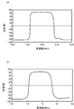
- FIG. 6A is a phase frequency characteristic diagram of the piezoelectric vibration device when the holding lengths DL1 and DL2 are 0.25 mm.
- FIG. 6B is a phase frequency characteristic diagram of the piezoelectric vibration device when the holding lengths DL1 and DL2 are 0.38 mm.
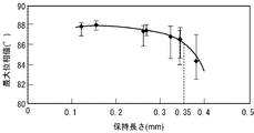
- FIG. 7 is a graph showing the relationship between the holding length and the maximum phase value (°) in the piezoelectric vibration device.
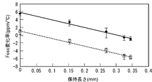
- FIG. 8 is a graph showing the relationship between the holding length and the Fosc change rate in the piezoelectric vibration device.
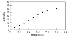
- FIG. 9 is a graph showing the relationship between the compressive stress generated in the piezoelectric vibrator and the holding length in the piezoelectric vibrator when the piezoelectric vibrator is cooled from 150 ° C.
- FIG. 10 is a stress distribution diagram of the piezoelectric vibration device when the holding length is 0.15 mm.
- FIG. 11 is a stress distribution diagram of the piezoelectric vibration device when the holding length is 0.35 mm.
- FIG. 12 is a schematic exploded perspective view of the piezoelectric vibration device according to the first modification.
- FIG. 13 is a schematic exploded perspective view of a piezoelectric vibration device according to a second modification.
- FIG. 14 is a side view of the piezoelectric resonance device disclosed in Patent Document 1. As shown in FIG.
- FIG. 1 is a schematic exploded perspective view of the piezoelectric vibration device of the present embodiment
- FIG. 2 is a schematic front sectional view of the piezoelectric vibration device of the present embodiment.
- the piezoelectric vibration device 1 of this embodiment includes a piezoelectric vibrator 20.
- the piezoelectric vibrator 20 includes a piezoelectric substrate 21 and first and second electrodes 22 and 23.
- the piezoelectric substrate 21 is made of a piezoelectric ceramic whose main crystal phase is a particle-oriented bismuth layered compound.
- the bismuth layered compound include Sr—Bi—Nb-based layered compounds, Sr—Bi—Ti-based layered compounds, and Ca—Bi—Ti-based layered compounds.
- Sr—Bi—Nb-based layered compound examples include, for example, SrBi 2 Nb 2 O 9 , (Sr (1-x) M x ) Bi 2 Nb 2 O 9 (where M is a divalent metal element, 0 ⁇ x ⁇ 0.3), (Sr (1-x) M 2x / 3 ) Bi 2 Nb 2 O 9 (where M is a trivalent metal element other than the element Bi constituting the main component, 0 ⁇ x ⁇ 0.45), SrBi 2 (Nb (1-y) Si y ) 2 O 9 (where 0 ⁇ y ⁇ 0.3), SrBi 2 (Nb (1-y) W y ) 2 O 9 (where , 0 ⁇ y ⁇ 0.3) and the like.
- Sr—Bi—Ti-based layered compound examples include SrBi 4 Ti 4 O 15 and Sr 2 Bi 4 Ti 5 O 18 .
- Ca—Bi—Ti layered compound examples include CaBi 4 Ti 4 O 15 and Ca 2 Bi 4 Ti 5 O 18 .
- other bismuth layered compounds include BiWO 6 , CaBi 2 Nb 2 O 9 , BaBi 2 Nb 2 O 9 , PbBi 2 Nb 2 O 9 , CaBi 2 Ta 2 O 9 , SrBi 2 Ta 2 O 9 , BaBi 2.
- the degree of orientation of the piezoelectric substrate 21 is not particularly limited as long as the piezoelectric substrate 21 vibrates when a voltage is applied, but is preferably 70% or more, and more preferably 75% or more.
- the degree of orientation of the piezoelectric substrate is specifically the degree of orientation in the crystal c-axis direction.
- the degree of orientation of the piezoelectric substrate is measured by the Lotgering method described in detail below.
- ⁇ I (hkl) and ⁇ I (001) are determined for the reflection intensity, and the ratio thereof is determined as P according to the following equation.
- P ⁇ I (001) / ⁇ I (hkl) ⁇
- the piezoelectric substrate 21 includes first and second main surfaces 21 a and 21 b facing each other, and first and second end surfaces 21 c and 21 d positioned at both ends in the longitudinal direction D of the piezoelectric substrate 21. have.
- a first electrode 22 is formed on the first main surface 21 a of the piezoelectric substrate 21.
- the first electrode 22 extends from the central portion in the longitudinal direction D of the first main surface 21a to the second main surface 21b side via the first end surface 21c.
- a second electrode 23 is formed on the second main surface 21 b of the piezoelectric substrate 21.
- the second electrode 23 extends from the central portion in the longitudinal direction D of the second main surface 21b to the first main surface 21a side via the second end surface 21d.
- An excitation portion 20a of the piezoelectric vibrator 20 is configured by a portion where the first and second electrodes 22 and 23 and the piezoelectric substrate 21 overlap in the thickness direction T.
- the piezoelectric substrate 21 is polarized along the longitudinal direction D of the piezoelectric substrate 21, and a voltage is applied between the first electrode 22 and the second electrode 23, whereby the longitudinal direction Thickness shear vibration with D as the vibration direction is excited.
- the piezoelectric vibrator 20 is mounted on the base material 10.
- a cap 30 is provided on the base material 10, and the piezoelectric vibrator 20 is sealed by the cap 30 and the base material 10.
- the material of the cap 30 is not specifically limited,
- the cap 30 can be comprised with a metal, a ceramic, resin, etc., for example.
- the base material 10 can be made of an insulating ceramic such as alumina.
- the substrate 10 is formed with first and second mounting electrodes 11 and 12.
- the first and second mounting electrodes 11 and 12 are disposed on both sides in the longitudinal direction of the substrate 10.
- the base material 10 and the piezoelectric vibrator 20 are joined by the first and second joining members 13 and 14.
- the first joining member 13 joins the first electrode 22 and the first mounting electrode 11.
- the second joining member 14 joins the second electrode 23 and the second mounting electrode 12.
- the first and second joining members 13 and 14 are made of, for example, a conductor such as a conductive adhesive, a conductive sheet, or solder, whereby the first and second electrodes 22 and 23 and the first and second electrodes
- the second mounting electrodes 11 and 12 are electrically connected.
- the piezoelectric substrate 21 is composed of piezoelectric ceramics having a grain-oriented bismuth layered compound as a main crystal phase as in this embodiment, the thickness-shear vibration is not confined, and both ends of the piezoelectric vibrator 20 are also vibrated. To do. As supported by an experimental example to be described later, the vibration displacement direction is reversed between both end portions of the piezoelectric vibrator 20 and the excitation portion 20a of the piezoelectric substrate 21.
- the first and second joining members 13 and 14 are joined to both ends of the piezoelectric vibrator 20 whose vibration displacement direction is opposite to that of the excitation part 20a. That is, the piezoelectric vibrator 20 is supported at both ends of the piezoelectric vibrator 20 whose vibration displacement direction is opposite to that of the excitation unit 20a.
- the end portion of the piezoelectric vibrator 20 whose vibration displacement direction is opposite to that of the excitation portion 20 a is along the longitudinal direction D between the excitation portion 20 a and the end portion from the end face of the piezoelectric vibrator 20.
- This is a portion up to 0.538 times the length ( ⁇ L).
- the 1st and 2nd joining members 13 and 14 have joined the base material 10 and the piezoelectric vibrator 20 so that the following formula
- the first and second joining members 13 and 14 are joined only to both ends of the piezoelectric vibrator 20 whose vibration displacement direction is opposite to that of the excitation part 20a.
- the piezoelectric vibrator 20 is preferably supported only at both ends of the piezoelectric vibrator 20 whose vibration displacement direction is opposite to that of the excitation unit 20a.
- the piezoelectric substrate 21 is composed of piezoelectric ceramics having a particle-oriented bismuth layered compound as a main crystal phase
- the first orientation can be obtained without changing the degree of orientation of the piezoelectric substrate 21.
- the lengths DL1 and DL2 of the joining surface between the first and second joining members 13 and 14 and the piezoelectric vibrator 20 can be easily adjusted. Therefore, for example, even when the degree of orientation of the piezoelectric substrate 21 varies, it is possible to easily suppress variation in temperature characteristics of the manufactured piezoelectric vibration device 1.
- the relationship between the orientation degree of the piezoelectric substrate 21 and the length DL is obtained experimentally or by simulation. Based on the relationship between the orientation degree of the piezoelectric substrate 21 and the length DL, the length DL that provides a preferable frequency-temperature characteristic is selected from the measurement result of the orientation degree of the piezoelectric substrate 21. Then, the piezoelectric vibrator 20 and the first and second mountings are arranged such that the length along the vibration direction D of the joint surface between the joining members 13 and 14 and the piezoelectric vibrator 20 becomes the selected length DL. The electrodes 11 and 12 are joined by the joining members 13 and 14. By doing so, for example, even when the orientation degree of the piezoelectric substrate 21 varies, the piezoelectric vibration device 1 having a desired frequency temperature characteristic can be stably manufactured.
- the effect that the oscillation characteristics are improved by joining the first and second joining members 13 and 14 to both ends of the piezoelectric vibrator 20 whose vibration displacement direction is opposite to that of the excitation part 20a is the effect of the piezoelectric vibration.
- the piezoelectric vibrator excites thickness shear vibration. Therefore, in the configuration of this embodiment in which the first and second joining members 13 and 14 are joined to both ends of the piezoelectric vibrator 20 whose vibration displacement direction is opposite to that of the excitation unit 20a, the piezoelectric vibrator is subjected to thickness shear vibration. It is particularly effective when exciting
- the above effect is particularly great when the bismuth layered compound is a Sr—Bi—Nb-based layered compound. Therefore, in the configuration of this embodiment in which the first and second bonding members 13 and 14 are bonded to both ends of the piezoelectric vibrator 20 whose vibration displacement direction is opposite to that of the excitation unit 20a, the bismuth layered compound is Sr-Bi. It is particularly effective when it is a —Nb-based layered compound.
- the vibration displacement distribution of the thickness shear vibration of the piezoelectric vibrator 20 in the non-fixed state was obtained using a finite element method (FEM).
- the piezoelectric material is Sr 0.9 Nd 0.1 Bi 2 Nb 2 O 9, and a piezoelectric substrate 21 that is polarized by applying a voltage of 4 kV / mm in the longitudinal direction D is used.
- the potential of the electrode 22 was 1V, and the potential of the second electrode 23 was 0V.
- Other detailed setting parameters are as follows. As a result, the resonance frequency of the piezoelectric vibrator 20 was 8 MHz.
- Length (L) along the longitudinal direction of the piezoelectric vibrator 20 2.2 mm Length (l) of the excitation unit 20a in which the first and second electrodes 22 and 23 overlap in the thickness direction T: 0.90 mm
- Thickness of the piezoelectric vibrator 20 190 ⁇ m
- Orientation degree 80%
- the vibration displacement distribution of the thickness shear vibration of a piezoelectric vibrator having the same setting parameters except that PZT was used as the piezoelectric material was obtained by a finite element method (FEM).
- FEM finite element method
- FIG. 3 is a diagram showing the vibration displacement distribution of the piezoelectric vibrator 20 when Sr 0.9 Nd 0.1 Bi 2 Nb 2 O 9 is used as the piezoelectric material
- FIG. 4 is a case where PZT is used as the piezoelectric material. It is a figure showing the vibration displacement distribution of the piezoelectric vibrator 20 of.
- FIG. 5 is a graph showing the relationship between the position along the longitudinal direction D of the piezoelectric vibrator 20 and the amount of vibration displacement. Use Incidentally, the graph shown by a solid line in FIG.
- a piezoelectric vibrator was actually produced under the same conditions as described above, and piezoelectric vibrators having various holding lengths DL1 and DL2 were produced using the piezoelectric vibrator. Note that an alumina substrate having a thickness of 0.4 mm was used as the substrate. Then, the phase frequency characteristics of the piezoelectric vibrators having various holding lengths DL1 and DL2 were measured.
- FIG. 6A shows a phase frequency characteristic diagram of the piezoelectric vibration device when the holding lengths DL1 and DL2 are 0.25 mm.
- FIG. 6B shows a phase frequency characteristic diagram of the piezoelectric vibration device when the holding lengths DL1 and DL2 are 0.38 mm.
- FIG. 7 is a graph showing the relationship between the holding lengths DL1 and DL2 and the maximum phase value (°) in the piezoelectric vibration device. As shown in FIG. 7, when the holding lengths DL1 and DL2 are less than 0.35 mm, a large maximum phase value can be obtained, but when the holding lengths DL1 and DL2 are 0.35 mm or more, the maximum phase value is obtained. It turns out that it falls rapidly.
- the graph indicated by the solid line indicates the Fosc change rate of the piezoelectric vibration device in which the degree of orientation of the piezoelectric substrate is 80.6%, and the graph indicated by the broken line indicates that the degree of orientation of the piezoelectric substrate is 77.5%.
- the Fosc change rate of a certain piezoelectric vibration device is shown.
- the inclination of the Fosc change rate of the piezoelectric vibration device in which the degree of orientation of the piezoelectric substrate is 80.6% is ⁇ 19.3 [ppm / ° C./mm], and the degree of orientation of the piezoelectric substrate is The slope of the Fosc change rate of the piezoelectric vibration device of 77.5% was ⁇ 19.5 [ppm / ° C./mm]. From this result, it can be seen that the frequency temperature characteristic of the piezoelectric vibrator changes when the degree of orientation of the piezoelectric substrate changes. Therefore, it can be seen that when the orientation degree of the piezoelectric substrate varies, the frequency temperature characteristics of the piezoelectric vibrator also vary. Therefore, when the holding lengths DL1 and DL2 are constant, it is necessary to stabilize the degree of orientation of the piezoelectric substrate at a high level in order to achieve good frequency temperature characteristics.
- the Fosc change rate changes. For this reason, even if the orientation degree of the piezoelectric substrate varies, the frequency temperature characteristics of the piezoelectric vibrator can be stabilized by adjusting the holding lengths DL1 and DL2. Specifically, for example, when the orientation degree is 80.6%, the Fosc change rate can be made zero by setting the holding lengths DL1 and DL2 to 0.30 mm, while the orientation degree is 77.degree. In the case of 5%, the Fosc change rate can be made zero by setting the holding lengths DL1 and DL2 to 0.07 mm.
- Fosc change rate ⁇ 19.3 ⁇ (holding length (DL)) + ⁇ (3)
- ⁇ is a constant determined by the degree of orientation of the piezoelectric substrate.
- FIG. 10 shows a stress distribution diagram of the piezoelectric vibration device when the holding lengths DL1 and DL2 are 0.15 mm
- FIG. 10 shows a stress distribution diagram of the piezoelectric vibration device when the holding lengths DL1 and DL2 are 0.35 mm. Is shown in FIG. In FIGS. 10 and 11, the area indicated by the lattice-like hatching is the area with the highest pressure, and the area indicated by the hatched hatching with the large interval is the area with the lowest pressure.
- the first and second mounting electrodes 11, 12 may be formed so as to reach the end surface of the substrate 10.
- a third mounting electrode that is not electrically connected to the first and second mounting electrodes 11 and 12 is used.
- the electrode 15 may be provided on the substrate 10. By providing the third mounting electrode 15, it is possible to incorporate a capacitor in the piezoelectric vibration device. Therefore, it is possible to reduce the number of parts of the device on which the piezoelectric vibration device is mounted.
Landscapes
- Physics & Mathematics (AREA)
- Acoustics & Sound (AREA)
- Piezo-Electric Or Mechanical Vibrators, Or Delay Or Filter Circuits (AREA)
Abstract
Description
0<DL1/ΔL1<0.538 ………式(1)
0<DL2/ΔL2<0.538 ………式(2)
無配向試料の各結晶面(hkl)からの反射強度をI(hkl)とし、それらの合計をΣI(hkl)とする。そのうち、(001)面からの反射強度I(001)の合計をΣI(001)として、それらの比P0を次式により求める。
P0={ΣI(001)/ΣI(hkl)}
P={ΣI(001)/ΣI(hkl)}
F={(P-P0)/(1-P0)}×100[%]
0<DL1/ΔL1<0.538 ………式(1)
0<DL2/ΔL2<0.538 ………式(2)
但し、
第1の接合部材13と圧電振動子20との接合面の振動方向Dに沿った長さ:DL1、
圧電振動子20の長手方向Dの一方側D1の端部から励振部20aまでの振動方向Dに沿った距離:ΔL1、
第2の接合部材14と圧電振動子20との接合面の振動方向Dに沿った長さ:DL2、
圧電振動子20の長手方向Dの他方側D2の端部から励振部20aまでの振動方向Dに沿った距離:ΔL2、
である。
非固定状態の圧電振動子20の厚みすべり振動の振動変位分布を有限要素法(FEM)を用いて求めた。なお、ここでは、圧電材料をSr0.9Nd0.1Bi2Nb2O9とし、長手方向Dに4kV/mmの電圧を印加して分極処理を行った圧電基板21を用い、第1の電極22の電位を1V、第2の電極23の電位を0Vとして行った。その他の詳細な設定パラメータは以下の通りである。この結果、この圧電振動子20の共振周波数は8MHzであった。
圧電振動子20の長手方向に沿った長さ(L):2.2mm
第1及び第2の電極22,23が厚み方向Tに重なっている励振部20aの長さ(l):0.90mm
圧電振動子20の厚み:190μm
配向度:80%
本実験例では、圧電基板の配向率以外は上記第1の実験例と同様の条件で圧電振動子を実際に作製し、その圧電振動子を用いて種々の保持長さDL1、DL2の圧電振動装置を作製した。そして、得られた圧電振動装置の共振周波数の温度変化率(Fosc変化率(ppm/℃))を測定した。Fosc変化率の測定結果を図8に示す。なお、図8において実線で示すグラフは、圧電基板の配向度が80.6%である圧電振動装置のFosc変化率を示し、破線で示すグラフは、圧電基板の配向度が77.5%である圧電振動装置のFosc変化率を示す。
(Fosc変化率)=-19.3×(保持長さ(DL))+α …… 式(3)
但し、上記式において、αは、圧電基板の配向度により決定される定数である。
次に、上記第1の実験例と同様の条件で、圧電振動装置を150℃から-40℃まで6℃/分で冷却したときに圧電振動子に生じる圧縮応力と、圧電振動装置における保持長さDL1,DL2との関係を、有限要素法(FEM)を用いて求めた。その結果を図9に示す。また、保持長さDL1,DL2が0.15mmである場合の圧電振動装置の応力分布図を図10に示し、保持長さDL1,DL2が0.35mmである場合の圧電振動装置の応力分布図を図11に示す。なお、図10及び図11において、格子状のハッチングで示す領域が最も圧力の高い領域で、間隔の大きな斜線ハッチングで示す領域が最も圧力の低い領域である。
図12に示すように、第1及び第2の実装用電極11,12は、基材10の端面に至るように形成されていてもよい。
10…基材
11…第1の実装用電極
12…第2の実装用電極
13…第1の接合部材
14…第2の接合部材
15…第3の実装用電極
20…圧電振動子
20a…励振部
21…圧電基板
21a…第1の主面
21b…第2の主面
21c…第1の端面
21d…第2の端面
22…第1の電極
23…第2の電極
30…キャップ
Claims (9)
- 対向する第1及び第2の主面を有しており、粒子配向されたビスマス層状化合物を主結晶相とする圧電基板と、前記圧電基板を介して厚み方向に対向するように前記第1及び第2の主面に形成された第1及び第2の電極とを有する圧電振動子と、
基材と、
前記基材と前記圧電振動子とを接合する接合部材とを備え、
前記圧電振動子は、前記第1及び第2の電極と前記圧電基板とが前記圧電基板の厚み方向に重なる部分により構成された励振部を有しており、
前記接合部材は、前記圧電振動子の前記励振部の振動変位方向とは振動変位方向が逆の部分に接合されている、圧電振動装置。 - 前記接合部材は、前記圧電振動子の前記励振部の振動変位方向とは振動変位方向が逆の部分のみに接合されている、請求項1に記載の圧電振動装置。
- 前記圧電振動子は、厚みすべり振動を励振させる、請求項1または2に記載の圧電振動装置。
- 前記接合部材は、前記圧電振動子の振動方向の一方側の端部を支持する第1の接合部材と、前記圧電振動子の振動方向の他方側の端部を支持する第2の接合部材とを有している、請求項3に記載の圧電振動装置。
- 前記第1の接合部材と前記圧電振動子との接合面の前記振動方向に沿った長さをDL1とし、前記圧電振動子の振動方向の一方側の端部から前記励振部までの前記振動方向に沿った距離をΔL1とし、前記第2の接合部材と前記圧電振動子との接合面の前記振動方向に沿った長さをDL2とし、前記圧電振動子の振動方向の他方側の端部から前記励振部までの前記振動方向に沿った距離をΔL2としたとき、以下の式(1)及び(2)を満たす、請求項4に記載の圧電振動装置。
0<DL1/ΔL1<0.538 ………式(1)
0<DL2/ΔL2<0.538 ………式(2) - 前記ビスマス層状化合物がSr-Bi-Nb系層状化合物である、請求項1~5のいずれか一項に記載の圧電振動装置。
- 前記基材には、前記第1の電極に電気的に接続された第1の実装用電極と、前記第2の電極に電気的に接続された第2の実装用電極と、前記第1及び第2の実装用電極に電気的に接続されていない第3の実装用電極とが形成されている、請求項1~6のいずれか一項に記載の圧電振動装置。
- 対向する第1及び第2の主面を有しており、粒子配向されたビスマス層状化合物を主結晶相とする圧電基板と、前記圧電基板を介して厚み方向に対向するように前記第1及び第2の主面に形成された第1及び第2の電極とを有する圧電振動子と、基材と、前記基材と前記圧電振動子とを接合する接合部材とを備え、前記圧電振動子は、前記第1及び第2の電極と前記圧電基板とが前記圧電基板の厚み方向に重なる部分により構成された励振部を有している圧電振動装置の製造方法であって、
前記圧電振動子の前記励振部の振動変位方向とは振動変位方向が逆の部分と前記基材とを前記接合部材により接合することを特徴とする、圧電振動装置の製造方法。 - 前記圧電振動子は、厚みすべり振動を励振させるものであり、
前記接合部材による前記圧電振動子と前記基材との接合は、前記接合部材と前記圧電振動子との接合面の前記圧電振動子の振動方向に沿った長さが前記圧電基板の配向度に応じて選択された長さとなるように行われる、請求項8に記載の圧電振動装置の製造方法。
Priority Applications (2)
| Application Number | Priority Date | Filing Date | Title |
|---|---|---|---|
| GB1103230.7A GB2475639B (en) | 2008-09-16 | 2009-05-08 | Piezoelectric oscillation device |
| JP2010529578A JP5045813B2 (ja) | 2008-09-16 | 2009-05-08 | 圧電振動装置 |
Applications Claiming Priority (2)
| Application Number | Priority Date | Filing Date | Title |
|---|---|---|---|
| JP2008-236155 | 2008-09-16 | ||
| JP2008236155 | 2008-09-16 |
Publications (1)
| Publication Number | Publication Date |
|---|---|
| WO2010032346A1 true WO2010032346A1 (ja) | 2010-03-25 |
Family
ID=42039199
Family Applications (1)
| Application Number | Title | Priority Date | Filing Date |
|---|---|---|---|
| PCT/JP2009/002013 Ceased WO2010032346A1 (ja) | 2008-09-16 | 2009-05-08 | 圧電振動装置 |
Country Status (2)
| Country | Link |
|---|---|
| JP (1) | JP5045813B2 (ja) |
| WO (1) | WO2010032346A1 (ja) |
Cited By (2)
| Publication number | Priority date | Publication date | Assignee | Title |
|---|---|---|---|---|
| JP2013021667A (ja) * | 2011-03-23 | 2013-01-31 | Nippon Dempa Kogyo Co Ltd | 水晶デバイス |
| US11510211B2 (en) | 2018-04-13 | 2022-11-22 | Vivo Mobile Communication Co., Ltd. | Sidelink operation method and terminal |
Citations (2)
| Publication number | Priority date | Publication date | Assignee | Title |
|---|---|---|---|---|
| JP2002043885A (ja) * | 2000-07-25 | 2002-02-08 | Tdk Corp | 圧電共振子、圧電共振部品及びその製造方法 |
| JP2005064689A (ja) * | 2003-08-08 | 2005-03-10 | Murata Mfg Co Ltd | 圧電共振子及び圧電共振部品 |
-
2009
- 2009-05-08 JP JP2010529578A patent/JP5045813B2/ja not_active Expired - Fee Related
- 2009-05-08 WO PCT/JP2009/002013 patent/WO2010032346A1/ja not_active Ceased
Patent Citations (2)
| Publication number | Priority date | Publication date | Assignee | Title |
|---|---|---|---|---|
| JP2002043885A (ja) * | 2000-07-25 | 2002-02-08 | Tdk Corp | 圧電共振子、圧電共振部品及びその製造方法 |
| JP2005064689A (ja) * | 2003-08-08 | 2005-03-10 | Murata Mfg Co Ltd | 圧電共振子及び圧電共振部品 |
Cited By (2)
| Publication number | Priority date | Publication date | Assignee | Title |
|---|---|---|---|---|
| JP2013021667A (ja) * | 2011-03-23 | 2013-01-31 | Nippon Dempa Kogyo Co Ltd | 水晶デバイス |
| US11510211B2 (en) | 2018-04-13 | 2022-11-22 | Vivo Mobile Communication Co., Ltd. | Sidelink operation method and terminal |
Also Published As
| Publication number | Publication date |
|---|---|
| JPWO2010032346A1 (ja) | 2012-02-02 |
| JP5045813B2 (ja) | 2012-10-10 |
Similar Documents
| Publication | Publication Date | Title |
|---|---|---|
| KR100669088B1 (ko) | 압전 진동자, 이를 이용한 필터 및 압전 진동자의 조정 방법 | |
| JP5457442B2 (ja) | 圧電素子の共振周波数の調整方法 | |
| CN1188918C (zh) | 压电陶瓷材料、烧结的压电陶瓷压块和压电陶瓷器件 | |
| CN108140723B (zh) | 压电元件、压电传声器、压电谐振子以及压电元件的制造方法 | |
| CN101847978A (zh) | 弯曲振动片及利用该弯曲振动片的振荡器 | |
| US9584093B2 (en) | Vibrating device | |
| CN101313456A (zh) | 超声波执行机构 | |
| CN110114968A (zh) | 用于振动波电机的压电振动器 | |
| KR100436637B1 (ko) | 압전트랜스포머 | |
| JPWO2010101026A1 (ja) | 薄膜圧電弾性波共振器及び高周波フィルタ | |
| WO2007088696A1 (ja) | 圧電振動装置 | |
| JP5045813B2 (ja) | 圧電振動装置 | |
| JP5232305B2 (ja) | 共振器および発振器 | |
| JP2010226609A (ja) | 振動片および振動子 | |
| KR100602907B1 (ko) | 복합 진동 장치 | |
| KR20010021310A (ko) | 압전 소자 | |
| GB2475639A (en) | Piezoelectric vibrator | |
| JP5589403B2 (ja) | 圧電共振子 | |
| US7446454B2 (en) | Thickness extensional piezoelectric resonator | |
| JP2008072156A (ja) | 複合材料振動装置 | |
| JP3760760B2 (ja) | 複合材料振動装置 | |
| JP2006041150A (ja) | 圧電トランス | |
| JP2026005960A (ja) | 振動片 | |
| Ochoa et al. | Vibration characteristic of cymbal type transducers | |
| JP2000165181A (ja) | 圧電共振子、電子部品および通信機器 |
Legal Events
| Date | Code | Title | Description |
|---|---|---|---|
| 121 | Ep: the epo has been informed by wipo that ep was designated in this application |
Ref document number: 09814192 Country of ref document: EP Kind code of ref document: A1 |
|
| WWE | Wipo information: entry into national phase |
Ref document number: 2010529578 Country of ref document: JP |
|
| ENP | Entry into the national phase |
Ref document number: 1103230 Country of ref document: GB Kind code of ref document: A Free format text: PCT FILING DATE = 20090508 |
|
| WWE | Wipo information: entry into national phase |
Ref document number: 1103230.7 Country of ref document: GB |
|
| NENP | Non-entry into the national phase |
Ref country code: DE |
|
| 122 | Ep: pct application non-entry in european phase |
Ref document number: 09814192 Country of ref document: EP Kind code of ref document: A1 |