WO2010029969A1 - 画像表示装置用表示粒子および画像表示装置 - Google Patents
画像表示装置用表示粒子および画像表示装置 Download PDFInfo
- Publication number
- WO2010029969A1 WO2010029969A1 PCT/JP2009/065831 JP2009065831W WO2010029969A1 WO 2010029969 A1 WO2010029969 A1 WO 2010029969A1 JP 2009065831 W JP2009065831 W JP 2009065831W WO 2010029969 A1 WO2010029969 A1 WO 2010029969A1
- Authority
- WO
- WIPO (PCT)
- Prior art keywords
- particles
- display
- inorganic fine
- display device
- image display
- Prior art date
- Legal status (The legal status is an assumption and is not a legal conclusion. Google has not performed a legal analysis and makes no representation as to the accuracy of the status listed.)
- Ceased
Links
Images

Classifications
-
- G—PHYSICS
- G02—OPTICS
- G02F—OPTICAL DEVICES OR ARRANGEMENTS FOR THE CONTROL OF LIGHT BY MODIFICATION OF THE OPTICAL PROPERTIES OF THE MEDIA OF THE ELEMENTS INVOLVED THEREIN; NON-LINEAR OPTICS; FREQUENCY-CHANGING OF LIGHT; OPTICAL LOGIC ELEMENTS; OPTICAL ANALOGUE/DIGITAL CONVERTERS
- G02F1/00—Devices or arrangements for the control of the intensity, colour, phase, polarisation or direction of light arriving from an independent light source, e.g. switching, gating or modulating; Non-linear optics
- G02F1/01—Devices or arrangements for the control of the intensity, colour, phase, polarisation or direction of light arriving from an independent light source, e.g. switching, gating or modulating; Non-linear optics for the control of the intensity, phase, polarisation or colour
- G02F1/165—Devices or arrangements for the control of the intensity, colour, phase, polarisation or direction of light arriving from an independent light source, e.g. switching, gating or modulating; Non-linear optics for the control of the intensity, phase, polarisation or colour based on translational movement of particles in a fluid under the influence of an applied field
- G02F1/166—Devices or arrangements for the control of the intensity, colour, phase, polarisation or direction of light arriving from an independent light source, e.g. switching, gating or modulating; Non-linear optics for the control of the intensity, phase, polarisation or colour based on translational movement of particles in a fluid under the influence of an applied field characterised by the electro-optical or magneto-optical effect
- G02F1/167—Devices or arrangements for the control of the intensity, colour, phase, polarisation or direction of light arriving from an independent light source, e.g. switching, gating or modulating; Non-linear optics for the control of the intensity, phase, polarisation or colour based on translational movement of particles in a fluid under the influence of an applied field characterised by the electro-optical or magneto-optical effect by electrophoresis
-
- G—PHYSICS
- G02—OPTICS
- G02F—OPTICAL DEVICES OR ARRANGEMENTS FOR THE CONTROL OF LIGHT BY MODIFICATION OF THE OPTICAL PROPERTIES OF THE MEDIA OF THE ELEMENTS INVOLVED THEREIN; NON-LINEAR OPTICS; FREQUENCY-CHANGING OF LIGHT; OPTICAL LOGIC ELEMENTS; OPTICAL ANALOGUE/DIGITAL CONVERTERS
- G02F1/00—Devices or arrangements for the control of the intensity, colour, phase, polarisation or direction of light arriving from an independent light source, e.g. switching, gating or modulating; Non-linear optics
- G02F1/01—Devices or arrangements for the control of the intensity, colour, phase, polarisation or direction of light arriving from an independent light source, e.g. switching, gating or modulating; Non-linear optics for the control of the intensity, phase, polarisation or colour
- G02F1/165—Devices or arrangements for the control of the intensity, colour, phase, polarisation or direction of light arriving from an independent light source, e.g. switching, gating or modulating; Non-linear optics for the control of the intensity, phase, polarisation or colour based on translational movement of particles in a fluid under the influence of an applied field
- G02F1/166—Devices or arrangements for the control of the intensity, colour, phase, polarisation or direction of light arriving from an independent light source, e.g. switching, gating or modulating; Non-linear optics for the control of the intensity, phase, polarisation or colour based on translational movement of particles in a fluid under the influence of an applied field characterised by the electro-optical or magneto-optical effect
- G02F1/1671—Devices or arrangements for the control of the intensity, colour, phase, polarisation or direction of light arriving from an independent light source, e.g. switching, gating or modulating; Non-linear optics for the control of the intensity, phase, polarisation or colour based on translational movement of particles in a fluid under the influence of an applied field characterised by the electro-optical or magneto-optical effect involving dry toners
-
- G—PHYSICS
- G02—OPTICS
- G02F—OPTICAL DEVICES OR ARRANGEMENTS FOR THE CONTROL OF LIGHT BY MODIFICATION OF THE OPTICAL PROPERTIES OF THE MEDIA OF THE ELEMENTS INVOLVED THEREIN; NON-LINEAR OPTICS; FREQUENCY-CHANGING OF LIGHT; OPTICAL LOGIC ELEMENTS; OPTICAL ANALOGUE/DIGITAL CONVERTERS
- G02F1/00—Devices or arrangements for the control of the intensity, colour, phase, polarisation or direction of light arriving from an independent light source, e.g. switching, gating or modulating; Non-linear optics
- G02F1/01—Devices or arrangements for the control of the intensity, colour, phase, polarisation or direction of light arriving from an independent light source, e.g. switching, gating or modulating; Non-linear optics for the control of the intensity, phase, polarisation or colour
- G02F1/165—Devices or arrangements for the control of the intensity, colour, phase, polarisation or direction of light arriving from an independent light source, e.g. switching, gating or modulating; Non-linear optics for the control of the intensity, phase, polarisation or colour based on translational movement of particles in a fluid under the influence of an applied field
- G02F1/1675—Constructional details
- G02F2001/1678—Constructional details characterised by the composition or particle type
-
- Y—GENERAL TAGGING OF NEW TECHNOLOGICAL DEVELOPMENTS; GENERAL TAGGING OF CROSS-SECTIONAL TECHNOLOGIES SPANNING OVER SEVERAL SECTIONS OF THE IPC; TECHNICAL SUBJECTS COVERED BY FORMER USPC CROSS-REFERENCE ART COLLECTIONS [XRACs] AND DIGESTS
- Y10—TECHNICAL SUBJECTS COVERED BY FORMER USPC
- Y10T—TECHNICAL SUBJECTS COVERED BY FORMER US CLASSIFICATION
- Y10T428/00—Stock material or miscellaneous articles
- Y10T428/29—Coated or structually defined flake, particle, cell, strand, strand portion, rod, filament, macroscopic fiber or mass thereof
- Y10T428/2982—Particulate matter [e.g., sphere, flake, etc.]
- Y10T428/2991—Coated
Definitions
- the present invention relates to an image display device capable of repeatedly executing display and erasing of images by moving the display particles in an electric field, and display particles used in the image display device.
- an image display device that displays an image by moving display particles in a gas phase.
- display particles are sealed in a powder form between two substrates, at least one of which is transparent, and an electric field is generated between the substrates to move and attach the display particles to one substrate.
- an electric field is generated by applying a voltage between the substrates, and the display particles move along the electric field direction. Therefore, an image can be displayed by appropriately selecting the electric field direction. And erasure can be executed repeatedly. For this reason, the image display device is required to display particles that can move smoothly even under a low driving voltage.
- Patent Documents 1 to 3 As display particles used in an image display device, those obtained by coating the surface of base particles with inorganic fine particles such as silica and titania are known (Patent Documents 1 to 3). In producing such display particles, the base particles and the inorganic fine particles are agitated and mixed under relatively strong conditions, so that the inorganic fine particles are fixed to the base particles.
- the adhesion of the display particles to the display particle contact surface between the substrates can be reduced.
- the drive voltage has not been sufficiently reduced, and further reduction of the drive voltage has been demanded.
- the drive voltage is set to a low voltage of 100 V, the contrast of the image is lowered, and the contrast is significantly reduced particularly during repeated driving.
- An object of the present invention is to provide display particles for an image display device that can repeatedly display an image having a relatively high contrast even when the drive voltage is relatively low, and an image display device including the display particles.
- the present invention relates to an image display device in which display particles are encapsulated in a powder form between two substrates, at least one of which is transparent, and an image is generated by moving the display particles by generating an electric field between the substrates.
- the present invention relates to a display particle for an image display device characterized by being 2.5% by weight and an image display device provided with the display particle for an image display device.
- the inorganic fine particles (external additive) externally added to the display particles not only exhibit the effect of reducing the adhesion of the display particles to the display particle contact surface between the substrates, but also between the display particles. It also has a bearing effect that reduces the impact force. Therefore, even when the driving voltage is relatively low, an image having a relatively high contrast can be repeatedly displayed.
- Display particles for image display devices include base particles and inorganic fine particles. Specifically, inorganic particles are externally added to the base particles.
- the display particles include those containing inorganic fine particles having relatively weak adhesion to the base particles.
- the release amount of inorganic fine particles having a primary particle size of 5 to 60 nm (hereinafter referred to as inorganic fine particles A) that are released when 60 ⁇ A ultrasonic energy is applied to the display particles in an aqueous polyoxyethyl phenyl ether solution for 1 minute.
- A is 0.1 to 2.5% by weight, preferably 0.2 to 0.6% by weight, based on the base particles.
- Such inorganic fine particles not only have the effect of reducing the adhesion of the display particles to the display particle contact surface between the substrates, but also exhibit a bearing effect that reduces the collision force between the display particles, so the driving voltage is compared. Even if the image is low, an image having a relatively high contrast can be repeatedly displayed. If the free amount A is too small, the bearing effect is not effectively exhibited, so that the driving voltage increases and the contrast decreases. If the amount A is too large, the free particles aggregate and increase in diameter, so that the bearing effect is not effectively exhibited. Inorganic fine particles having a too small particle size or inorganic fine particles having a too large particle size do not exhibit the bearing effect effectively, so the drive voltage increases and the contrast decreases.
- the primary particle size means the particle size of the primary particles, and in the present invention, the inorganic fine particles A having such a primary particle size may have a form of an aggregate. This is because the inorganic fine particles A are relatively easily broken when the image display device is driven even if they have the form of aggregates.
- the free amount X of all inorganic fine particles released when ultrasonic energy of 300 ⁇ A is applied for 60 minutes in an aqueous polyoxyethyl phenyl ether solution is usually 0.1 to 20% by weight based on the base particles, In particular, it is 1 to 10% by weight.
- the free amount A / free amount X is preferably 0.01 to 0.99, particularly preferably 0.05 to 0.1.
- the free amount A and free amount X can be measured by the following method.
- the image display device is disassembled as it is to take out display particles.
- (Procedure 2) 20 g of display particles are put in a 300 cc beaker, mixed with 200 g of a 0.2% aqueous solution (dispersion medium) of polyoxyethyl phenyl ether, and sufficiently wetted.
- (Procedure 3) With an ultrasonic homogenizer US-1200T (manufactured by Nippon Seiki Co., Ltd .; specification frequency 15 kHz), the value of the ammeter indicating the vibration instruction value attached to the main unit is 60 ⁇ A (50 w). And apply for 1 minute to release inorganic fine particles.
- the above-mentioned measuring device for the particle size distribution is for measuring the particle size distribution of the primary particles forming the aggregate even if the inorganic fine particles have the form of the aggregate.
- the ammeter value is 300 ⁇ A and the application time of ultrasonic energy is 60 minutes in Procedure 3, the total weight Wx ( g) is measured.
- the base particles obtained as a residue by filtration are sufficiently dried, and the weight Wc (g) of the base particles is measured.
- the inorganic fine particles A are not particularly limited as long as they have the above primary particle diameter.
- metal oxides such as silicon oxide, titanium oxide, aluminum oxide, tin oxide, zirconium oxide, and tungsten oxide, and nitridation such as titanium nitride Products, titanium compounds, and mixtures thereof.
- the inorganic fine particles A are preferably silicon oxide.
- the inorganic fine particles A preferably have hydrophobicity from the viewpoint of more effectively obtaining the effect of reducing the adhesion of the display particles to the display particle contact surfaces between the substrates. Hydrophobicity is imparted by treating inorganic fine particles with a hydrophobizing agent.
- the hydrophobizing agent is not particularly limited, and any silane coupling agent such as dichlorosilane, alkoxysilane, silazane, aminosilane, or silylated isocyanate can be used.
- the inorganic fine particles A preferably exhibit a degree of hydrophobicity of 30 to 99.
- the value measured by methanol wettability is used as the degree of hydrophobicity.
- the inorganic fine particles B may be used in combination with the inorganic fine particles A.
- the free amount B of the inorganic fine particles B which is released when an ultrasonic energy of 60 ⁇ A is applied for 1 minute in a polyoxyethyl phenyl ether aqueous solution is usually 1% by weight or less, particularly 0%. 0.01 to 0.3% by weight.
- the inorganic fine particles B are made of the same material as the inorganic fine particles A except that the primary particle diameter is different from that of the inorganic fine particles A, and is preferably silicon oxide.
- the primary particle size of the inorganic fine particles B is usually more than 60 nm and 250 nm or less, preferably 65 nm or more and 200 nm or less.
- the inorganic fine particles B preferably have hydrophobicity, and preferably have a degree of hydrophobicity within the same range as the inorganic fine particles A.
- the free amount B can be measured by the same method as the free amount A except that the weight of the inorganic fine particles B having a predetermined particle diameter is obtained from the total weight and particle size distribution of the free inorganic fine particles.
- the display particles of the present invention can be produced by the following method (A).
- Method (A) For example, relatively small agitation using a mixing device that can uniformly mix with a relatively weak agitation force such as a turbuler mixer (Glen Mills), a Henschel mixer (Mitsui Miike Seisakusho), a super mixer (Kawata)
- a relatively weak agitation force such as a turbuler mixer (Glen Mills), a Henschel mixer (Mitsui Miike Seisakusho), a super mixer (Kawata)
- the base particles and the inorganic fine particles a are mixed at a speed and a relatively short mixing time (weak condition mixing process).
- the inorganic fine particles a are those containing at least the inorganic fine particles A having the above-mentioned particle size, and usually further containing the inorganic fine particles B, and those having an average primary particle size of 5 to 55 nm, particularly 14 to 40 nm are preferably used.
- the free amount A can be controlled by adjusting the content of the inorganic fine particles A contained in the inorganic fine particles a. For example, the free amount A increases as the content of the inorganic fine particles A increases, and the free amount A decreases as the content decreases.
- inorganic fine particles a having an inorganic fine particle A content of 50% by weight or more, particularly 70 to 99% by weight, based on the total amount of the inorganic fine particles a.
- the constituent material of the inorganic fine particles a the same materials as the inorganic fine particles A can be exemplified.
- the inorganic fine particles a two or more types of inorganic fine particles having different average primary particle sizes and / or constituent materials may be used.
- the average primary particle diameter of the inorganic fine particles is the number average particle diameter of the primary particles (number-based median diameter (d50 diameter)), and a value calculated from an image taken with a scanning electron microscope is used.
- a scanning electron microscope “JSM-7410” manufactured by JEOL Ltd. was used to take a 100000 times photograph of the particle, and each of the 200 particles had a maximum length (any two points on the circumference of the particle). The maximum length) is measured, and the number average value is defined as the average particle diameter.
- the particle size of the primary particles forming the aggregates is measured.
- the turbulent mixer (manufactured by GlenGMills Co., Ltd.) achieves mixing using beads, and forms fine particles of primary particles while crushing aggregates of fine inorganic particles with beads. Therefore, the bearing effect of the inorganic fine particles A can be obtained more effectively.
- the liberation amount A can also be controlled by adjusting the production conditions, particularly the mixing conditions. Specifically, for example, when using a turbuler mixer (manufactured by Glen Mills), the stirring speed is set to 20 to 300 rpm, preferably 50 to 250 rpm, and the mixing time is set to 3 to 20 minutes, preferably 5 to 10 minutes.
- the average particle size of the beads is 0.1 to 10 mm, preferably 0.5 to 5 mm.
- the stirring speed is decreased within the above range, the mixing time is shortened within the above range, or the average particle size of the beads is increased within the above range, the free amount A increases.
- the stirring speed is increased within the above range, the mixing time is increased within the above range, or the average particle size of the beads is decreased within the above range, the free amount A decreases. If the stirring speed is too large, the mixing time is too long, or the average particle size of the beads is too small, the inorganic fine particles A are relatively strongly immobilized on the base particles, so that the free amount A Is less than the specified range. If the stirring speed is too low, the mixing time is too short, or the average particle size of the beads is too large, the inorganic fine particles A will remain as aggregates without being crushed, and the inner wall of the apparatus Since it adheres to the beads, the free amount A is less than the specified range.
- the stirring speed is 15 to 40 m / second, preferably 20 to 30 m / second, and the mixing time is 5 to 30 minutes, preferably 10 to 20 minutes. Is set.
- the stirring speed is decreased within the above range or the mixing time is shortened within the above range, the free amount A increases.
- the stirring speed is increased within the above range or the mixing time is increased within the above range, the free amount A decreases. If the stirring speed is too large or the mixing time is too long, and the inorganic fine particles A are relatively strongly immobilized on the base particles, the free amount A is less than the specified range. If the stirring speed is too low or the mixing time is too short and it is out of the above range, the inorganic fine particles A are not crushed and remain as agglomerates and further adhere to the inner wall of the apparatus. Less than the specified range.
- the amount of the inorganic fine particles a added is not particularly limited as long as the above-mentioned free amount A is achieved, and usually 0.1 to 3% by weight, particularly preferably 0.2 to 1% by weight or less based on the base particles.
- the display particles of the present invention can also be produced by the following method (B).
- Method (B) In the method (A), the inorganic fine particles C are immobilized on the base particles in advance. That is, after the pretreatment for fixing the inorganic fine particles C to the base particles is performed, the method (A) is performed. Thereby, the inorganic fine particles A function more effectively on the inorganic fine particles C on the surface of the base particles, and the effect of reducing the adhesion of the display particles to the display particle contact surface between the substrates and the bearing effect are further improved.
- “Immobilization” means a phenomenon in which a part of the inorganic fine particles C is integrated into the base particles by being embedded in the base particles.
- the inorganic fine particles C When immobilization of the inorganic fine particles C is achieved, most of the inorganic fine particles C will not be liberated even if ultrasonic energy is applied under the same conditions as in the method of measuring the liberation amount A. It does not prevent C from being liberated.
- the inorganic fine particles C When the inorganic fine particles C are liberated under the above conditions, the inorganic fine particles C having a predetermined particle diameter may be measured as the inorganic fine particles A when the amount of liberation A is measured.
- the inorganic fine particles C can be made of the same material as the inorganic fine particles A except that the particle size is not particularly limited, and is preferably silicon oxide.
- the inorganic fine particles C those having an average primary particle size of 60 to 250 nm, preferably 70 to 200 nm are usually used.
- the inorganic fine particles C preferably have hydrophobicity, and preferably have a degree of hydrophobicity within the same range as the inorganic fine particles A.
- a mixing apparatus that can uniformly mix with a relatively strong stirring force such as a Henschel mixer (manufactured by Mitsui Miike Mining Co., Ltd.), a super mixer (manufactured by Kawata Co., Ltd.),
- the base particles and the inorganic fine particles C are mixed at a high stirring speed and a relatively long mixing time (strong condition mixing process).
- the stirring speed is set to 30 to 70 m / second, preferably 40 to 60 m / second, and the mixing time is set to 10 to 60 minutes, preferably 20 to 40 minutes.
- the instantaneous heat treatment is a heat treatment in which hot air is instantaneously blown against an object to be processed.
- the heating temperature is a temperature at which the above-described immobilization is achieved and the particles are not completely buried or fused between the same kind of particles, and may be determined depending on, for example, the weight average molecular weight of the base particles. Specifically, when the base particles have a weight average molecular weight of about 5,000 to 200,000, the heating temperature is usually 80 to 300 ° C.
- a commercially available hot-air spheronizer (Surfing System SFS-3 manufactured by Nippon Pneumatic Industry) is available as an apparatus capable of performing such instantaneous heat treatment.
- the amount of the inorganic fine particles C added is not particularly limited, and for example, it is preferably 200% by weight or less, particularly preferably 1 to 10% by weight or less based on the base particles.
- the display particles usually include positively-charged display particles and negatively-charged display particles, and each display particle is formed by adding inorganic fine particles to base particles.
- the free amount A, the free amount X and the free amount B in the mixture of the positively charged display particles and the negatively charged display particles, and the relationship thereof may be within the above ranges, respectively.
- the positively charged display particles and the negatively charged display particles can be independently produced by the above-described method (A) or method (B).
- both positively charged display particles and negatively charged display particles are produced by the method (B).
- the positively charged display particles and the negatively charged display particles have a predetermined polarity, for example, by frictional contact with each other or by frictional contact with a reference material such as iron powder (carrier) as a charge imparting material. Is charged.
- the charge polarity can be controlled by, for example, the type of resin or charge control agent contained in the base particles.
- the base particles are colored resin particles containing at least a resin and a colorant, and are included in the base particles included in the positively charged display particles and the negatively charged display particles. Different colorants are contained in the base particles.
- the color difference means that when an electric field is generated between the substrates in the image display device described in detail later, the display particles moved and adhered to the substrate on the upstream side in the viewing direction and the residue on the substrate on the downstream side in the viewing direction -It means that there is a difference in hue, lightness, saturation, etc. between the attached display particles.
- the display image can be visually recognized based on such a difference.
- white base particles and black base particles are used in combination.
- the color can be controlled by the type of colorant contained in the base particles (black: carbon black, iron oxide, aniline black, white: titanium oxide, zinc oxide, zinc sulfide).
- the resin constituting the base particle is not particularly limited, and a polymer called a vinyl resin shown below is a typical one.
- a polymer called a vinyl resin shown below is a typical one.
- a polyamide resin or a polyester resin examples thereof include condensation resins such as polycarbonate resins and epoxy resins.
- vinyl resins include, for example, polyolefin resins formed from ethylene monomers and propylene monomers, in addition to polystyrene resins, polyacrylic resins, and polymethacrylic resins.
- resins other than vinyl resins include polyether resins, polysulfone resins, polyurethane resins, fluorine resins, and silicone resins in addition to the above-described condensation resins.
- the polymer constituting the resin that can be used for the base particles is produced by combining a plurality of types of polymerizable monomers in addition to those obtained by using at least one type of polymerizable monomer that forms these resins. You can also.
- a resin is produced by combining a plurality of types of polymerizable monomers, for example, a method of forming a copolymer such as a block copolymer, a graft copolymer or a random copolymer, or a mixture of a plurality of types of resins.
- resin formation by a polymer blending method There is also resin formation by a polymer blending method.
- base particles containing styrene acrylic resin, acrylic resin, and fluorine resin tend to be negatively charged, so the base particles are useful for negatively charged display particles. It is. Further, for example, since the base particles containing a polyamide-based resin or a polymethacrylic resin tend to be positively charged, the base particles are useful for positively charged display particles.
- the weight average molecular weight of the resin constituting the base particles is usually 5000 to 200000, particularly 15000 to 100,000.
- the weight average molecular weight is a value measured by HLC-8220 (manufactured by Tosoh Corporation).
- the colorant is not particularly limited, and pigments known in the field of electrophotographic toner are used.
- the white pigment constituting the white base particles includes, for example, zinc oxide (zinc white), titanium oxide, antimony white, zinc sulfide, barium titanate, calcium titanate, strontium titanate, and the like.
- titanium oxide is preferable.
- examples of the black pigment constituting the black base particles include carbon black, copper oxide, manganese dioxide, aniline black, activated carbon, and the like. Among these, carbon black is preferable.
- the content of the colorant is not particularly limited, and may be, for example, 1 to 200 parts by weight with respect to 100 parts by weight of the resin.
- the base particles may contain a charge control agent employed in the field of electrophotographic toner, if desired.
- the charge control agent is not particularly limited, and a charge control agent known in the field of electrophotographic toner is used.
- base particles containing a negative charge control agent such as a salicylic acid metal complex, a metal-containing azo dye, a quaternary ammonium salt compound, or a nitrimidazole derivative are useful as negatively charged display particles.
- host particles containing a positive charge control agent such as a nigrosine dye, a triphenylmethane compound, or an imidazole derivative are useful as positively charged display particles.
- the content of the charge control agent is not particularly limited, and may be, for example, 0.1 to 10 parts by weight with respect to 100 parts by weight of the resin.
- the volume average particle diameter D1 of the base particles is 1 to 50 ⁇ m, preferably 1 to 30 ⁇ m.
- the volume average particle diameter of all the base particles of the positively charged display particle base particles and the negatively charged display particle base particles is D1, and the value is the above It may be within the range. If D1 is too small, the van der Waals force increases and the display particles aggregate to reduce the contrast. On the other hand, if D1 is too large, the stress at the time of driving increases due to the influence of the weight of the particles, and the external additive is buried, so that the repeated characteristics deteriorate.
- the volume average particle diameter D1 of the base particles is a volume-based median diameter (d50 diameter), and is measured and calculated using an apparatus in which a computer system for data processing is connected to Multisizer 3 (manufactured by Beckman Coulter). be able to.
- a measurement procedure 0.02 g of a sample is conditioned with 20 ml of a surfactant solution (for dispersing particles, a surfactant solution obtained by diluting a neutral detergent containing a surfactant component 10 times with pure water). After that, ultrasonic dispersion is performed for 1 minute to prepare a dispersion.
- This dispersion is injected into a beaker containing ISOTON II (manufactured by Beckman Coulter, Inc.) in a sample stand with a pipette until the measured concentration reaches 10%, and measurement is performed with a measuring machine count set to 2500 pieces.
- the aperture size of the multisizer 3 is 50 ⁇ m.
- the method for producing the base particles is not particularly limited, and for example, a known method for producing particles containing a resin and a colorant, such as a method for producing a toner used for electrophotographic image formation, is applied. It is possible to cope with it.
- Specific examples of the method for producing the base particles include the following methods.
- a method of producing base particles through kneading and classification steps after kneading a resin and a colorant (2) a so-called suspension polymerization method in which a polymerizable monomer and a colorant are mechanically stirred in an aqueous medium to form droplets and then polymerized to produce base particles; (3) A polymerizable monomer is dropped into an aqueous medium containing a surfactant and polymerized in micelles to produce polymer particles of 100 to 150 nm.
- a so-called emulsion polymerization aggregation method in which base particles are produced by adding and aggregating and fusing these particles.
- An image display device is characterized by including the above-described display particles.
- the image display apparatus of the present invention will be described in detail.
- the image display device according to the present invention is also called a “powder display”.
- the image display device encloses the display particles described above in a powder form between two substrates, at least one of which is transparent, and moves the display particles by generating an electric field between the substrates. An image is displayed.
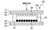
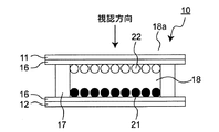
- FIG. 1 shows a typical cross section of an image display device according to the present invention.
- FIG. 1A shows a structure in which an electrode 15 having a layer structure is provided on substrates 11 and 12 and an insulating layer 16 is provided on the surface of the electrode 15.
- the image display device shown in FIG. 1B has a structure in which no electrode is provided in the device, and an electric field is applied through an electrode provided outside the device so that display particles can be moved. It is.
- the same reference numerals in FIGS. 1A and 1B denote the same members.
- FIG. 1 is meant to include FIGS. 1 (a) and 1 (b).
- the image display device 10 in FIG. 1 is configured to visually recognize an image from the substrate 11 side.
- the image display device 10 is not limited to an image viewed from the substrate 11 side.
- the type shown in FIG. 1B has an advantage that the structure of the device can be simplified and the manufacturing process can be shortened because the electrode 15 is not provided in the device itself.
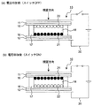
- FIG. 3 shows a state in which voltage application is performed by setting the image display device 10 of the type shown in FIG.
- the cross-sectional configuration of the image display device according to the present invention is not limited to that shown in FIGS.
- two substrates 11 and 12 which are casings constituting the image display device are arranged to face each other.
- an electrode 15 for applying a voltage is provided on the surface on which both faces each other, and an insulating layer 16 is provided on the electrode 15.
- the substrates 11 and 12 are provided with an electrode 15 and an insulating layer 16, and display particles exist in a gap 18 formed by facing the surfaces having the electrode 15 and the insulating layer 16.
- two types of display particles, black display particles (hereinafter referred to as black particles) 21 and white display particles (hereinafter referred to as white particles) 22 are present in the gap 18 as display particles. .
- the resin fine particles and the inorganic fine particles are externally added to the surfaces of the black particles 21 and the white particles 22, but they are not illustrated. Further, in the image display device 10 of FIG. 1, the gap 18 is surrounded by the substrates 11 and 12 and the two partition walls 17, and the display particles are present in a state of being enclosed in the gap 18.
- the thickness of the gap 18 is not particularly limited as long as the enclosed display particles can move and maintain the contrast of the image, and is usually 10 ⁇ m to 500 ⁇ m, preferably 10 ⁇ m to 100 ⁇ m.
- the volume occupation ratio of the display particles in the gap 18 is 5% to 70%, preferably 30% to 60%.
- the behavior of display particles in the gap 18 of the image display device 10 will be described.
- the image display device according to the present invention when a voltage is applied between two substrates to form an electric field, the charged display particles move along the electric field direction. In this way, by applying a voltage between the substrates on which display particles exist, the charged display particles move between the substrates to perform image display.
- the image display in the image display apparatus is performed by the following procedure.
- the display particles used as the display medium are charged by a known method such as frictional charging with a carrier.
- Display particles are sealed between two opposing substrates, and a voltage is applied between the substrates in this state.
- An electric field is formed between the substrates by applying a voltage between the substrates.
- the display particles are attracted to the surface of the substrate along the direction of the electric field opposite to the polarity of the display particles by the action of the electric field force between the electrodes, so that image display can be performed.
- the moving direction of the display particles is switched by changing the electric field direction between the substrates.
- the image display can be changed variously by switching the moving direction.
- the display particles can be charged by the above-described known methods, for example, a method in which the display particles are charged by contact with a carrier by frictional charging, or two color display particles having different charging polarities are mixed and stirred.
- a carrier it is preferable to use a carrier and enclose the charged display particles in a substrate.
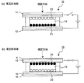
- FIG. 2A shows a state before a voltage is applied between the substrates 11 and 12, and positively charged white particles 22 are present in the vicinity of the substrate 11 on the viewing side before the voltage is applied.
- the image display device 10 displays a white image.
- FIG. 2B shows a state after a voltage is applied to the electrode 15, and the black particles 21 that are negatively charged by applying a positive voltage to the substrate 11 are located near the substrate 11 on the viewing side.
- the white particles 22 have moved to the substrate 12 side.
- the image display device 10 displays a black image.
- FIG. 3 shows a state in which the image display device 10 shown in FIG. 1B without an electrode is set in the voltage application device 30 and a voltage is not applied in this state (FIG. 3A). ) And a state after the voltage is applied (FIG. 3B).
- the black particles 21 negatively charged by applying a positive voltage to the substrate 11 as well as the image display device 10 having the electrode 15 are in the vicinity of the substrate 11 on the viewing side.
- the positively charged white particles 22 have moved to the substrate 12 side.
- the substrates 11 and 12 constituting the image display device 10 will be described.
- the observer visually recognizes the image formed by the display particles from at least one side of the substrates 11 and 12, and therefore the substrate provided on the side viewed by the observer is required to be made of a transparent material.
- the substrate used on the side where the observer visually recognizes the image is preferably a light-transmitting material having a visible light transmittance of 80% or more, for example, and has a visible light transmittance of 80% or more. Sex is obtained.
- the material of the substrate provided on the opposite side of the image viewing side is not necessarily transparent.
- each of the substrates 11 and 12 is preferably 2 ⁇ m to 5 mm, and more preferably 5 ⁇ m to 2 mm.
- the thicknesses of the substrates 11 and 12 are in the above range, sufficient strength can be given to the image display device 10 and the distance between the substrates can be kept uniform.
- the image display device can be provided in a compact and lightweight manner by setting the thickness of the substrate within the above range, the use of the image display device in a wide field is promoted. Further, by setting the thickness of the substrate on the side where the image is viewed to be in the above range, the display image can be accurately viewed without impeding the display quality.
- Examples of the material having a visible light transmittance of 80% or more include non-flexible inorganic materials such as glass and quartz, organic materials typified by resin materials described later, and metal sheets. Among these, organic materials and metal sheets can impart a certain degree of flexibility to the image display device.
- Examples of the resin material having a visible light transmittance of 80% or more include polyester resins typified by polyethylene terephthalate and polyethylene naphthalate, polycarbonate resins, polyethersulfone resins, and polyimide resins. .
- a vinyl polymerizable monomer such as an acrylic resin or a polyethylene resin, which is a polymer of acrylic acid ester or methacrylic acid ester represented by polymethyl methacrylate (PMMA). It is done.
- the electrode 15 is provided on the surfaces of the substrates 11 and 12, and forms an electric field between the substrates, that is, the gap 18 by applying a voltage. As with the above-described substrate, it is necessary to provide a transparent electrode 15 on the side where the observer visually recognizes the image.
- the thickness of the electrode provided on the side where the image is viewed is required to ensure electrical conductivity and to a level that does not hinder the light transmission. Specifically, the thickness is preferably 3 nm to 1 ⁇ m, and preferably 5 nm to 400 nm. More preferred. Note that the visible light transmittance of the electrode provided on the side where the image is viewed is preferably 80% or more, like the substrate. The thickness of the electrode provided on the side opposite to the side where the image is viewed is also preferably within the above range, but it is not necessary to be transparent.
- Examples of the constituent material of the electrode 15 include a metal material, a conductive metal oxide, or a conductive polymer material.
- Specific examples of the metal material include aluminum, silver, nickel, copper, and gold.
- Specific examples of the conductive metal oxide include indium tin oxide (ITO), indium oxide, and antimony tin.
- ITO indium tin oxide
- ATO antimony tin
- examples of the conductive polymer material include polyaniline, polypyrrole, polythiophene, polyacetylene, and the like.
- a method for forming the electrode 15 on the substrate 11 or 12 for example, when an electrode on a thin film is provided, a sputtering method, a vacuum evaporation method, a chemical vapor deposition method (CVD method; chemical vapor deposition), a coating method, or the like can be used. Can be mentioned. There is also a method of forming an electrode by mixing a conductive material with a solvent or a binder resin and applying the mixture to a substrate.
- the insulating layer 16 is provided on the surface of the electrode 15 and is in contact with the display particles 21 and 22 on the surface of the insulating layer 16, but is not necessarily provided.
- the insulating layer 16 has a role of relaxing the change in the charge amount by the voltage applied when the display particles 21 and 22 are moved. Further, by imparting a resin having a highly hydrophobic structure and unevenness, it is possible to reduce the physical adhesion with the display particles and to reduce the driving voltage.
- the material constituting the insulating layer 16 is an electrically insulating material that can be made into a thin film, and has transparency as desired.
- the insulating layer provided on the image viewing side preferably has a visible light transmittance of 80% or more, like the substrate. Specific examples include silicone resin, acrylic resin, and polycarbonate resin.
- the thickness of the insulating layer 16 is preferably 0.01 ⁇ m or more and 10.0 ⁇ m or less. That is, when the thickness of the insulating layer 16 is in the above range, the display particles 21 and 22 can move without applying a very large voltage between the electrodes 15. For example, a voltage at a level applied in image formation by electrophoresis is applied. It is preferable because the image can be displayed by applying.
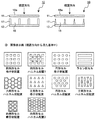
- the partition wall 17 secures a gap 18 between the upper and lower substrates, and can be formed not only at the edges of the substrates 11 and 12 but also inside as needed, as shown in the right and left diagrams in the upper part of FIG. .
- the width of the partition wall 17, particularly the thickness of the partition wall on the image display surface 18 a side, is preferably as thin as possible from the viewpoint of ensuring the clarity of the display image, as shown in the right side of FIG.
- the partition walls 17 formed inside the substrates 11 and 12 may be formed continuously in the front and back directions or intermittently in the drawings on the right and left sides in the upper part of FIG.
- the cells in the gap 18 partitioned by the partition walls 17 can be arranged in various shapes.
- An example of the shape and arrangement of the cells when the gap 18 is viewed from the viewing direction of the substrate 11 is shown in the lower diagram of FIG.
- a plurality of cells can be arranged in a rectangular shape, a triangular shape, a line shape, a circular shape, a hexagonal shape, etc., in a honeycomb shape or a mesh shape.
- the partition wall 17 can be formed, for example, by processing the substrate on the side opposite to the side where the image is viewed using the following method.
- Examples of the method for forming the partition wall 17 include embossing with a resin material or the like, uneven formation by hot press injection molding, photolithography, screen printing, and the like.
- Example 1 [Manufacture of white display particles] (White matrix particles)
- the resin and titanium oxide described below were put into a Henschel mixer (manufactured by Mitsui Miike Mining Co., Ltd.), the peripheral speed of the stirring blade was set to 25 m / second, and the mixture was mixed for 5 minutes to obtain a mixture.
- Styrene acrylic resin weight average molecular weight 20,000
- Anatase type titanium oxide average primary particle size 150 nm
- the above mixture was kneaded with a twin-screw extrusion kneader and then coarsely pulverized with a hammer mill.
- the mixture was pulverized by a turbo mill pulverizer (manufactured by Turbo Kogyo Co., Ltd.), and further finely classified by an airflow classifier utilizing the Coanda effect to produce white base particles having a volume average particle size of 10.0 ⁇ m.
- Black matrix particles The resin and carbon black described below were put into a Henschel mixer (manufactured by Mitsui Miike Mining Co., Ltd.), the peripheral speed of the stirring blade was set to 25 m / sec, and the mixture was mixed for 5 minutes to obtain a mixture.
- Styrene acrylic resin weight average molecular weight 20,000 100 parts by weight
- Carbon black average primary particle size 25 nm 10 parts by weight
- the above mixture is kneaded with a twin-screw extrusion kneader, then coarsely pulverized with a hammer mill, and then turbo milled.
- Coarse powder was pulverized with a machine (manufactured by Turbo Kogyo Co., Ltd.), and further finely classified with an airflow classifier utilizing the Coanda effect to produce black base particles having a volume average particle diameter of 10.0 ⁇ m.
- silica particles having an average primary particle size of 15 nm (hydrophobic degree 92%) subjected to silazane-based coupling agent hexamethyldisilazane treatment, and an average primary particle size of 1 mm 300 parts by weight of the glass beads were placed in a 500 cc pot, and mixed with a turbuler mixer (Glen Mills) at 100 rpm for 5 minutes. Glass beads were removed from the obtained mixture with a mesh sieve to obtain black display particles. In the silica particles, the content of primary particles having a primary particle size of 5 to 60 nm was 82% by weight.
- Carrier A for charging white display particles Conditions in which 2 parts of fluorinated acrylate resin particles are added to 100 parts by weight of ferrite core having an average particle diameter of 80 ⁇ m, and these raw materials are put into a horizontal rotary blade type mixer so that the peripheral speed of the horizontal rotary blade is 8 m / sec. was mixed and stirred at 22 ° C. for 10 minutes, and then heated to 90 ° C. and stirred for 40 minutes to produce Carrier A.
- Carrier B for charging black display particles Under the condition that 2 parts of cyclohexyl methacrylate resin particles are added to 100 parts by weight of a ferrite core having an average particle diameter of 80 ⁇ m, and these raw materials are put into a horizontal rotary blade type mixer so that the peripheral speed of the horizontal rotary blade is 8 m / sec. After mixing and stirring at 22 ° C. for 10 minutes, carrier B was produced by heating to 90 ° C. and stirring for 40 minutes.
- the image display apparatus was manufactured according to the following method so as to have the same structure as that shown in FIG.
- Two glass substrates 11 having a length of 80 mm, a width of 50 mm, and a thickness of 0.7 mm are prepared, and each substrate surface is made of an indium tin oxide (ITO) film (resistance 30 ⁇ / ⁇ ) having a thickness of 300 nm.
- ITO indium tin oxide
- the electrode 15 was formed by a vapor deposition method.
- a coating solution prepared by dissolving 12 g of polycarbonate resin in a mixed solvent of 80 ml of tetrahydrofuran and 20 ml of cyclohexanone is applied by spin coating to form an insulating layer 16 having a thickness of 3 ⁇ m.
- the display particles were charged by mixing 1 g of black display particles and 9 g of carrier B using a shaker (YS-LD, manufactured by Yayoi Co., Ltd.) for 30 minutes. As shown in FIG. 5A, the obtained mixture (21, 210) was placed on a conductive stage 100, and one substrate with electrodes was placed at an interval of about 2 mm from the stage 100. Between the electrode 15 and the stage 100, a DC bias of +50 V, an AC bias of 2.0 kV, and a frequency of 2.0 kHz were applied for 10 seconds to deposit the black display particles 21 on the insulating layer 16.
- a DC bias of +50 V, an AC bias of 2.0 kV, and a frequency of 2.0 kHz were applied for 10 seconds to deposit the black display particles 21 on the insulating layer 16.
- the display particles were charged by mixing 30 g of white display particles 1 g and carrier A 9 g with a shaker (YS-LD, manufactured by Yayoi Co., Ltd.) for 30 minutes. As shown in FIG. 5B, the obtained mixture (22, 220) was placed on a conductive stage 100, and the other substrate with electrodes was placed at a distance of about 2 mm from the stage 100. Between the electrode 15 and the stage 100, a DC bias of ⁇ 50 V, an AC bias of 2.0 kV, and a frequency of 2.0 kHz were applied for 10 seconds to adhere the white display particles 22 on the insulating layer 16.
- a DC bias of ⁇ 50 V, an AC bias of 2.0 kV, and a frequency of 2.0 kHz were applied for 10 seconds to adhere the white display particles 22 on the insulating layer 16.
- the substrate with electrodes to which black display particles are attached and the substrate with electrodes to which white display particles are attached are adjusted and overlapped with a partition so as to have an interval of 50 ⁇ m.
- the volume occupation ratio between the two types of display particles between the glass substrates was 50%.
- the content ratio of the white display particles and the black display particles is approximately 1/1 in the number ratio of the white display particles / black display particles.
- Example 2 An image display device was manufactured by the same method as in Example 1 except that white display particles and black display particles manufactured by the following method were used.
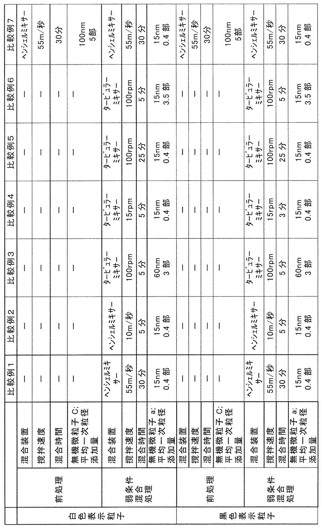
- Examples 3 to 6 Comparative Examples 1 to 6> An image display device was manufactured by the same method as in Example 2 except that white display particles and black display particles manufactured by the following method were used.
- White display particles and black display particles were produced by the same method as the production method of white display particles and black display particles of Example 2, except that the weak condition mixing treatment was performed according to the conditions described in the table.
- Example 7 An image display device was manufactured by the same method as in Example 1 except that white display particles and black display particles manufactured by the following method were used.
- White display particles and black display particles were produced by the same method as the production method of white display particles and black display particles of Example 1, except that the pretreatment and the weak condition mixing treatment were performed according to the conditions described in the table. .
- the inorganic fine particles having an average primary particle size of 30 nm used for the production of the white display particles are silica particles (hydrophobic degree 80%) surface-treated with aminopropyltrimethoxysilane.
- the content of primary particles having a primary particle size of 5 to 60 nm was 72% by weight.
- the inorganic fine particles having an average primary particle size of 40 nm used for the production of the white display particles are silica particles (hydrophobic degree 78%) surface-treated with aminopropyltrimethoxysilane.
- the content of primary particles having a primary particle size of 5 to 60 nm was 58% by weight.
- the inorganic fine particles having an average primary particle size of 60 nm used for the production of the white display particles are silica particles (hydrophobic degree 76%) surface-treated with aminopropyltrimethoxysilane.
- the content of primary particles having a primary particle size of 5 to 60 nm was 32% by weight.
- the inorganic fine particles having an average primary particle size of 30 nm used for the production of black display particles are silica particles (hydrophobic degree 90%) surface-treated with hexamethyldisilazane.
- the content of primary particles having a primary particle size of 5 to 60 nm was 75% by weight.
- the inorganic fine particles having an average primary particle size of 40 nm used for the production of black display particles are silica particles (hydrophobic degree 88%) surface-treated with hexamethyldisilazane.
- the content of primary particles having a primary particle size of 5 to 60 nm was 61% by weight.
- the inorganic fine particles having an average primary particle size of 60 nm used for the production of black display particles are silica particles (hydrophobic degree 89%) surface-treated with hexamethyldisilazane.
- the content of primary particles having a primary particle size of 5 to 60 nm was 34% by weight.
- the display characteristics were evaluated by applying a DC voltage to the image display device according to the following procedure and measuring the reflection density of the display image obtained by the voltage application.
- the voltage application was performed according to the following procedure. The applied voltage was changed from 0V to the plus side, then changed to the minus side, and the voltage was applied so as to draw a hysteresis curve of a path returning to 0V again. That is, (1) Application is performed while changing the voltage from 0V to + 100V at intervals of 20V. (2) Application is performed while changing the voltage from + 100V to ⁇ 100V at intervals of 20V. (3) Application is performed while changing the voltage from ⁇ 100V to 0V at intervals of 20V.
- contrast was evaluated as display characteristics, and repeated characteristics were evaluated.
- the black density is the reflection density of the display surface obtained when a voltage of +100 V is applied to the electrode on the upstream side in the viewing direction of the image display device.
- the white density is the reflection density of the display surface obtained when a voltage of ⁇ 100 V is applied to the electrode on the upstream side in the viewing direction of the image display device.
- the density was measured at five locations on the display surface at random using a reflection densitometer “RD-918 (manufactured by Macbeth)”, and the average value was obtained. Contrast of density difference of 1.30 or more was rated as best ( ⁇ ), 1.20 or higher as excellent ( ⁇ ), 1.00 or higher as pass ( ⁇ ), and less than 1.00 as reject (x).
- the repetition characteristics were evaluated based on the number of repetitions when the contrast became 0.70 or less when the voltage density of +100 V and ⁇ 100 V were alternately repeated and the reflection density was measured each time.
- the number of repetitions was 5000 (excellent), 1000 (exclusive) was acceptable ( ⁇ ), and less than 1000 was unacceptable (x).
- the minimum drive voltage is a voltage when the display density value becomes 0.7 or more when the applied voltage is changed at intervals of 5V from 0V to 200V.
- the minimum drive voltage is 60 V or less, the best ( ⁇ ), 80 V or less is excellent ( ⁇ ), 100 V or less is acceptable ( ⁇ ), and when it exceeds 100 V, it is regarded as unacceptable (X).
Landscapes
- Physics & Mathematics (AREA)
- Nonlinear Science (AREA)
- Health & Medical Sciences (AREA)
- Life Sciences & Earth Sciences (AREA)
- Chemical & Material Sciences (AREA)
- Chemical Kinetics & Catalysis (AREA)
- Electrochemistry (AREA)
- Molecular Biology (AREA)
- General Physics & Mathematics (AREA)
- Optics & Photonics (AREA)
- Electrochromic Elements, Electrophoresis, Or Variable Reflection Or Absorption Elements (AREA)
Abstract
Description
少なくとも樹脂および着色剤を含有する母体粒子および該母体粒子に外添される無機微粒子を含み、
表示粒子に対してポリオキシエチルフェニルエーテル水溶液中で60μAの超音波エネルギーを1分間付与したときに遊離する一次粒径5~60nmの無機微粒子の遊離量Aが母体粒子に対して0.1~2.5重量%であることを特徴とする画像表示装置用表示粒子および該画像表示装置用表示粒子を備えた画像表示装置に関する。
本発明に係る画像表示装置用表示粒子(以下、単に表示粒子という)は、母体粒子および無機微粒子を含み、詳しくは母体粒子に無機微粒子が外添されてなるものである。
本明細書中、一次粒径は一次粒子の粒径を意味し、本発明においてそのような一次粒径を有する無機微粒子Aは凝集体の形態を有していてもよい。無機微粒子Aは凝集体の形態を有していても、画像表示装置の駆動時において比較的容易に解砕されるためである。
(手順1)画像表示装置をそのまま分解して表示粒子を取り出す。
(手順2)表示粒子20gを300ccビーカーに入れ、ポリオキシエチルフェニルエーテルの0.2%水溶液(分散媒体)200gと混合し、十分に濡れさせる。
(手順3)超音波式ホモジナイザーUS-1200T(日本精機社製;仕様周波数 15kHz)にて、超音波エネルギーを、本体装置に付属の振動指示値を示す電流計の値が60μA(50w)を示すように調整し、1分間印加して無機微粒子を遊離させる。
(手順4)混合液を目開き1μmのろ紙で吸引ろ過し、得られたろ液から分散媒体を蒸発させて、遊離無機微粒子を分離し、十分に乾燥させる。
(手順5)遊離無機微粒子の総重量を測定し、さらにマイクロトラックUPA-150(日機装社製)により粒径分布を測定する。それらの結果から、所定粒径の無機微粒子の重量を求め、一次粒径5~60nmの無機微粒子の重量をWa(g)とする。粒径分布の上記測定装置は、無機微粒子が凝集体の形態を有していても、凝集体を形成する一次粒子の粒度分布を測定するものである。
(手順6)手順3において電流計の値を300μA、超音波エネルギーの付与時間を60分間とすること以外、上記手順1~5と同様の操作手順により、全ての遊離無機微粒子の総重量Wx(g)を測定する。
(手順7)手順6において、ろ過によって残渣として得られた母体粒子を十分に乾燥させ、母体粒子の重量Wc(g)を測定する。
(手順8)以下の式に従って母体粒子基準の遊離量Aおよび遊離量Xを求める。
遊離量A(重量%)=(Wa/Wc)×100
遊離量X(重量%)=(Wx/Wc)×100
疎水化度はメタノールウェッタビリティーによって測定された値を用いている。メタノールウェッタビリティーとは、メタノールに対する濡れ性を評価するものである。この方法は、内容量200mlのビーカー中に入れた蒸留水50mlに、測定対象の無機微粒子を0.2g秤量し添加する。メタノールを先端が液体中に浸漬されているビュレットから、ゆっくり撹拌した状態で無機微粒子の全体が濡れるまでゆっくり滴下する。この無機微粒子を完全に濡らすために必要なメタノールの量をa(ml)とした場合に、下記式により疎水化度が算出される。
疎水化度={a/(a+50)}×100
方法(A);
例えば、タービュラーミキサー(Glen Mills社製)、ヘンシェルミキサー(三井三池製作所社製)、スーパーミキサー(カワタ社製)等のような比較的弱い撹拌力で均一に混合できる混合装置により、比較的小さな撹拌速度および比較的短い混合時間で母体粒子と無機微粒子aを混合する(弱条件混合処理)。
無機微粒子aの構成材料としては無機微粒子Aと同様のものが例示できる。無機微粒子aは平均一次粒径または/および構成材料が異なる2種類以上の無機微粒子が使用されてよい。
測定手順としては、走査型電子顕微鏡「JSM-7410」(日本電子社製)を用いて粒子の100000倍の写真を撮影し、粒子200個についてそれぞれ最大長(粒子の周上の任意の2点間のうち最大の長さ)を測定し、その個数平均値を平均粒径とする。尚、粒子が凝集体として撮影される場合には、凝集体を形成する一次粒子の粒径を測定するものとする。
具体的には、例えばタービュラーミキサー(Glen Mills社製)を使用する場合、撹拌速度は20~300rpm、好ましくは50~250rpmに、混合時間は3~20分間、好ましくは5~10分間に設定され、ビーズの平均粒径は0.1~10mm、好ましくは0.5~5mmである。撹拌速度を上記範囲内で小さくしたり、混合時間を上記範囲内で短くしたり、ビーズの平均粒径を上記範囲内で大きくしたりすると、遊離量Aは増大する。撹拌速度を上記範囲内で大きくしたり、混合時間を上記範囲内で長くしたり、ビーズの平均粒径を上記範囲内で小さくしたりすると、遊離量Aは減少する。撹拌速度が大きすぎたり、混合時間が長すぎたり、ビーズの平均粒径が小さすぎたりして上記範囲外となると、無機微粒子Aが母体粒子に比較的強く固定化されるため、遊離量Aが前記規定範囲より少なくなる。撹拌速度が小さすぎたり、混合時間が短かすぎたり、ビーズの平均粒径が大きすぎたりして上記範囲外となると、無機微粒子Aは解砕されず凝集塊のまま存在し、さらに装置内壁やビーズに付着するので、遊離量Aが前記規定範囲より少なくなる。
方法(B);
前記方法(A)において母体粒子に予め無機微粒子Cを固定化させておく。すなわち、母体粒子に無機微粒子Cを固定化させる前処理を実施した後で、前記方法(A)を実施する。これにより、無機微粒子Aが母体粒子表面の無機微粒子C上でより一層有効に機能し、基板間における表示粒子接触面に対する表示粒子の付着力低減効果およびベアリング効果がより向上する。「固定化」は、無機微粒子Cの一部が母体粒子に埋没されることによって母体粒子に一体化される現象を意味するものとする。
正帯電の表示粒子および負帯電の表示粒子のいずれにおいても、母体粒子は少なくとも樹脂および着色剤を含有する着色樹脂粒子であり、正帯電表示粒子に含まれる母体粒子と、負帯電表示粒子に含まれる母体粒子とで、異なる色の着色剤が含まれる。
本明細書中、重量平均分子量はHLC-8220(東ソー社製)によって測定された値を用いている。
測定手順としては、サンプル0.02gを界面活性剤溶液20ml(粒子を分散させるためのもので、界面活性剤成分を含む中性洗剤を純水で10倍希釈した界面活性剤溶液)で馴染ませた後、超音波分散を1分間行い、分散液を作製する。この分散液を、サンプルスタンド内のISOTONII(ベックマン・コールター社製)の入ったビーカーに、測定濃度10%になるまでピペットにて注入し、測定機カウントを2500個に設定して測定する。なお、マルチサイザー3のアパチャー径は50μmのものを使用する。
(1)樹脂と着色剤とを混練した後、粉砕、分級の各工程を経て母体粒子を製造する方法;
(2)水系媒体中で重合性単量体と着色剤を機械的に撹拌して液滴を形成した後、重合を行って母体粒子を製造する、いわゆる懸濁重合法;
(3)界面活性剤を含有させた水系媒体中に重合性単量体を滴下し、ミセル中で重合反応を行って100~150nmの重合体粒子を製造した後、着色剤粒子と凝集剤を添加してこれらの粒子を凝集・融着させて母体粒子を製造する、いわゆる乳化重合凝集法。
本発明に係る画像表示装置は上記した表示粒子を備えたことを特徴とする。以下、本発明の画像表示装置について詳細に説明する。なお、本発明に係る画像表示装置は、「粉体ディスプレイ」とも呼ばれるものである。
本発明に係る画像表示装置は、2枚の基板間に電圧を印加されて電界が形成されると、帯電している表示粒子は電界方向に沿って移動する様になる。この様に、表示粒子が存在する基板間に電圧を印加することにより、帯電した表示粒子が基板間を移動して画像表示を行うものである。
(1)表示媒体として用いる表示粒子を、キャリアによる摩擦帯電等の公知の方法により帯電させる。
(2)対向する2枚の基板間に表示粒子を封入し、この状態で基板間に電圧を印加する。
(3)基板間への電圧印加により、基板間に電界が形成される。
(4)表示粒子は、電極間の電界の力の作用により表示粒子の極性と反対側の電界方向に沿って基板表面に引き寄せられ、画像表示が行える様になる。
(5)また、基板間の電界方向を変えることにより、表示粒子の移動方向を切り換える。この移動方向の切換えにより画像表示を様々に変えることができる。
図2(a)は、基板11と12の間に電圧を印加する前の状態を示しており、電圧印加前は視認側の基板11近傍には正帯電した白色粒子22が存在している。この状態は画像表示装置10が白色画像を表示しているものである。また、図2(b)は、電極15に電圧を印加した後の状態を示しており、基板11に正の電圧を印加することで負に帯電した黒色粒子21が視認側の基板11近傍に移動し、白色粒子22は基板12側に移動している。この状態は画像表示装置10が黒色画像を表示しているものである。
隔壁17の形状および配置を制御することにより、隔壁17により仕切られた隙間18のセルを様々な形状で配置できる。隙間18を基板11の視認方向から見た時のセルの形状および配置の例を図4下段の図に示す。セルは、図4下段の図に示すように、四角形状、三角形状、ライン状、円形状、六角形状等にて、複数個で、ハニカム状や網目状に配置することができる。
[白色表示粒子の製造]
(白色母体粒子)
下記した樹脂及び酸化チタンをヘンシェルミキサ(三井三池鉱業社製)に投入し、撹拌羽根の周速を25m/秒に設定して5分間混合処理して混合物とした。
スチレンアクリル樹脂(重量平均分子量20,000) 100重量部
アナタース型酸化チタン(平均一次粒径150nm) 30重量部
上記混合物を二軸押出混練機で混練し、次いで、ハンマーミルで粗粉砕した後、ターボミル粉砕機(ターボ工業社製)で粉砕処理し、さらに、コアンダ効果を利用した気流分級機で微粉分級処理を行って、体積平均粒径が10.0μmの白色母体粒子を製造した。
白色母体粒子100重量部に、アミノシラン系カップリング剤(アミノプロピルトリメトキシシラン)処理を行った平均一次粒径が100nmのシリカ粒子(疎水化度75%)5重量部を添加し、ヘンシェルミキサー(三井三池鉱業社製)に投入し、撹拌羽根の周速(撹拌速度)を55m/秒に設定して30分間混合処理を行った。
(瞬間的加熱処理)
その後、得られた混合物に対して、熱風球形化装置(日本ニューマチック工業製;サーフュージングシステムSFS-3型)を用いて、入り口の熱風温度100℃、熱風流量1.0m3、原料投入速度1.0kg/hで、熱風処理時間を0.03sとして瞬間的加熱処理を行った。
(弱条件混合処理)
引き続き、得られた混合物と、アミノシラン系カップリング剤(アミノプロピルトリメトキシシラン)処理を行った平均一次粒径が15nmのシリカ粒子(疎水化度78%)0.4重量部と、平均一次粒径が1mmのガラスビーズ300重量部を500ccのポットに入れ、タービュラーミキサー(Glen Mills社製)により100rpmにて5分間混合処理を行った。得られた混合物をメッシュ篩にてガラスビーズを除去し、白色表示粒子を得た。当該シリカ粒子において一次粒径5~60nmの一次粒子の含有量は80重量%であった。
(黒色母体粒子)
下記した樹脂及びカーボンブラックをヘンシェルミキサ(三井三池鉱業社製)に投入し、撹拌羽根の周速を25m/秒に設定して5分間混合処理して混合物とした。
スチレンアクリル樹脂(重量平均分子量20,000) 100重量部
カーボンブラック(平均一次粒径25nm) 10重量部
上記混合物を二軸押出混練機で混練し、次いで、ハンマーミルで粗粉砕した後、ターボミル粉砕機(ターボ工業社製)で粗粉粉砕し、さらに、コアンダ効果を利用した気流分級機で微粉分級処理を行って、体積平均粒径が10.0μmの黒色母体粒子を製造した。
黒色母体粒子100重量部に、シラザン系カップリング剤ヘキサメチルジシラザン処理を行った平均一次粒径が100nmのシリカ粒子(疎水化度88%)5重量部を添加し、ヘンシェルミキサー(三井三池鉱業社製)に投入し、撹拌羽根の周速(撹拌速度)を55m/秒に設定して30分間混合処理を行った。
(瞬間的加熱処理)
その後、得られた混合物に対して、熱風球形化装置(日本ニューマチック工業製;サーフュージングシステムSFS-3型)を用いて、入り口の熱風温度100℃、熱風流量1.0m3、原料投入速度1.0kg/hで、熱風処理時間を0.03sとして瞬間的加熱処理を行った。
(弱条件混合処理)
引き続き、得られた混合物と、シラザン系カップリング剤ヘキサメチルジシラザン処理を行った平均一次粒径が15nmのシリカ粒子(疎水化度92%)0.4重量部と、平均一次粒径が1mmのガラスビーズ300重量部を500ccのポットに入れ、タービュラーミキサー(Glen Mills社製)により100rpmにて5分間混合処理を行った。得られた混合物をメッシュ篩にてガラスビーズを除去し、黒色表示粒子を得た。当該シリカ粒子において一次粒径5~60nmの一次粒子の含有量は82重量%であった。
平均粒子径80μmのフェライトコア100重量部に対して、フッ素化アクリレート樹脂粒子を2部加え、これら原料を水平回転翼型混合機に投入し、水平回転翼の周速が8m/秒となる条件で22℃で10分間混合攪拌した後、90℃に加熱し40分攪拌して、キャリアAを製造した。
平均粒子径80μmのフェライトコア100重量部に対して、シクロヘキシルメタクリレート樹脂粒子を2部加え、これら原料を水平回転翼型混合機に投入し、水平回転翼の周速が8m/秒となる条件で22℃で10分間混合攪拌した後、90℃に加熱し40分攪拌して、キャリアBを製造した。
画像表示装置は、図1(a)と同様の構造を有するように、以下の方法に従って製造した。長さ80mm、幅50mm、厚さ0.7mmのガラス基板11を2枚用意し、各基板面上には、厚さ300nmのインジウム・スズ酸化物(ITO)被膜(抵抗30Ω/□)からなる電極15を蒸着法により形成した。上記電極上に、ポリカーボネート樹脂12gを、テトラヒドロフラン80mlとシクロヘキサノン20mlの混合溶媒に溶解させてなる塗布液を、スピンコート法により塗布して厚さ3μmの絶縁層16を形成し、一対の電極付き基板を得た。
以下の方法で製造した白色表示粒子および黒色表示粒子を用いたこと以外、実施例1と同様の方法により、画像表示装置を製造した。
(弱条件混合処理)
実施例1と同様の白色母体粒子100重量部と、アミノシラン系カップリング剤(アミノプロピルトリメトキシシラン)処理を行った平均一次粒径が15nmのシリカ粒子(疎水化度78%)0.4重量部と、平均一次粒径が1mmのガラスビーズ300重量部を500ccのポットに入れ、タービュラーミキサー(Glen Mills社製)により100rpmにて5分間混合処理を行った。得られた混合物をメッシュ篩にてガラスビーズを除去し、白色表示粒子を得た。当該シリカ粒子において一次粒径5~60nmの一次粒子の含有量は80重量%であった。
(弱条件混合処理)
実施例1と同様の黒色母体粒子100重量部と、シラザン系カップリング剤ヘキサメチルジシラザン処理を行った平均一次粒径が15nmのシリカ粒子(疎水化度92%)0.3重量部と、平均一次粒径が1mmのガラスビーズ300重量部を500ccのポットに入れ、タービュラーミキサー(Glen Mills社製)により100rpmにて5分間混合処理を行った。得られた混合物をメッシュ篩にてガラスビーズを除去し、黒色表示粒子を得た。当該シリカ粒子において一次粒径5~60nmの一次粒子の含有量は82重量%であった。
以下の方法で製造した白色表示粒子および黒色表示粒子を用いたこと以外、実施例2と同様の方法により、画像表示装置を製造した。
弱条件混合処理を表に記載の条件に従って行ったこと以外、実施例2の白色表示粒子および黒色表示粒子の製造方法と同様の方法により、それぞれ白色表示粒子および黒色表示粒子を製造した。
以下の方法で製造した白色表示粒子および黒色表示粒子を用いたこと以外、実施例1と同様の方法により、画像表示装置を製造した。
前処理および弱条件混合処理を表に記載の条件に従って行ったこと以外、実施例1の白色表示粒子および黒色表示粒子の製造方法と同様の方法により、それぞれ白色表示粒子および黒色表示粒子を製造した。

白色表示粒子の製造に使用した平均一次粒径40nmの無機微粒子は、アミノプロピルトリメトキシシランで表面処理したシリカ粒子(疎水化度78%)である。一次粒径5~60nmの一次粒子の含有量は58重量%であった。
白色表示粒子の製造に使用した平均一次粒径60nmの無機微粒子は、アミノプロピルトリメトキシシランで表面処理したシリカ粒子(疎水化度76%)である。一次粒径5~60nmの一次粒子の含有量は32重量%であった。
黒色表示粒子の製造に使用した平均一次粒径40nmの無機微粒子は、ヘキサメチルジシラザンで表面処理したシリカ粒子(疎水化度88%)である。一次粒径5~60nmの一次粒子の含有量は61重量%であった。
黒色表示粒子の製造に使用した平均一次粒径60nmの無機微粒子は、ヘキサメチルジシラザンで表面処理したシリカ粒子(疎水化度89%)である。一次粒径5~60nmの一次粒子の含有量は34重量%あった。
画像表示装置に対して以下の手順で直流電圧を印加し、電圧印加により得られる表示画像の反射濃度を測定することにより、表示特性を評価した。尚、電圧印加は、以下の手順で行い、印加電圧を0Vからプラス側に変化させた後、続いてマイナス側に変化させ、再び0Vに戻る経路のヒステリシス曲線を描く様に電圧を印加した。すなわち、
(1)0Vから+100Vまで20V間隔で電圧を変化させながら印加を行う。
(2)+100Vから-100Vまで20V間隔で電圧を変化させながら印加を行う。
(3)-100Vより0Vまで20V間隔で電圧を変化させながら印加を行う。
上記手順で各画像表示装置に直流電圧を印加したところ、白表示の状態でプラスの電圧を印加した時に、表示が白から黒に変化することが確認された。なお、画像表示装置の視認方向上流側の電極に印加する電圧を変化させ、他方の電極は電気的に接地させた。濃度は、反射濃度計「RD-918(マクベス社製)」を用いて測定した。
(コントラスト)
コントラストは、黒色濃度と白色濃度との差、すなわち、
コントラスト=黒色濃度-白色濃度
で定義される濃度差により評価した。
黒色濃度は、画像表示装置の視認方向上流側の電極に+100Vの電圧を印加した時に得られる表示面の反射濃度である。
白色濃度は、画像表示装置の視認方向上流側の電極に-100Vの電圧を印加した時に得られる表示面の反射濃度である。
濃度は、反射濃度計「RD-918(マクベス社製)」を用いて、表示面上の5カ所をランダムに測定して、その平均値とした。
コントラストは、濃度差が1.30以上を最優良(◎)、1.20以上を優良(○)、1.00以上を合格(△)、1.00未満を不合格(×)とした。
繰り返し特性は、+100Vと-100Vの電圧印加を交互に繰り返し、その都度反射濃度を測定したとき、コントラストが0.70以下になった時点での繰り返し回数に基づいて評価した。繰り返し回数が5000回以上を優良(○)、1000回以上を合格(△)、1000回未満を不合格(×)とした。
最小駆動電圧は、0Vから200Vまで5V間隔で印加電圧を変化させた時、表示濃度の値が0.7以上となる時の電圧である。最小駆動電圧が60V以下を最優良(◎)、80V以下を優良(○)、100V以下を合格(△)、100Vを超えると不合格(×)とした。

Claims (6)
- 少なくとも一方が透明な2枚の基板間に表示粒子を粉体形態で封入し、該基板間に電界を発生させることによって、該表示粒子を移動させて画像を表示する画像表示装置に用いられる表示粒子であって、
少なくとも樹脂および着色剤を含有する母体粒子および該母体粒子に外添される無機微粒子を含み、
表示粒子に対してポリオキシエチルフェニルエーテル水溶液中で60μAの超音波エネルギーを1分間付与したときに遊離する一次粒径5~60nmの無機微粒子の遊離量Aが母体粒子に対して0.1~2.5重量%であることを特徴とする画像表示装置用表示粒子。 - 表示粒子に対してポリオキシエチルフェニルエーテル水溶液中で300μAの超音波エネルギーを60分間付与したときに遊離する全無機微粒子の遊離量Xが母体粒子に対して0.1~20重量%である請求項1に記載の画像表示装置用表示粒子。
- 遊離量A/遊離量Xが0.01~0.99である請求項2に記載の画像表示装置用表示粒子。
- 少なくとも一方が透明な2枚の基板間に表示粒子を粉体形態で封入し、該基板間に電界を発生させることによって、該表示粒子を移動させて画像を表示する画像表示装置であって、
前記表示粒子が、少なくとも樹脂および着色剤を含有する母体粒子および該母体粒子に外添される無機微粒子を含むものであり、
前記表示粒子に対してポリオキシエチルフェニルエーテル水溶液中で60μAの超音波エネルギーを1分間付与したときに遊離する一次粒径5~60nmの無機微粒子の遊離量Aが母体粒子に対して0.1~2.5重量%であることを特徴とする画像表示装置。 - 表示粒子に対してポリオキシエチルフェニルエーテル水溶液中で300μAの超音波エネルギーを60分間付与したときに遊離する全無機微粒子の遊離量Xが母体粒子に対して0.1~20重量%である請求項4に記載の画像表示装置。
- 遊離量A/遊離量Xが0.01~0.99である請求項5に記載の画像表示装置。
Priority Applications (2)
| Application Number | Priority Date | Filing Date | Title |
|---|---|---|---|
| JP2010508145A JP5099217B2 (ja) | 2008-09-12 | 2009-09-10 | 画像表示装置用表示粒子および画像表示装置 |
| US12/745,448 US20100302622A1 (en) | 2008-09-12 | 2009-09-10 | Display particles for image display device and image display device installed with the same |
Applications Claiming Priority (2)
| Application Number | Priority Date | Filing Date | Title |
|---|---|---|---|
| JP2008-234894 | 2008-09-12 | ||
| JP2008234894 | 2008-09-12 |
Publications (1)
| Publication Number | Publication Date |
|---|---|
| WO2010029969A1 true WO2010029969A1 (ja) | 2010-03-18 |
Family
ID=42005219
Family Applications (1)
| Application Number | Title | Priority Date | Filing Date |
|---|---|---|---|
| PCT/JP2009/065831 Ceased WO2010029969A1 (ja) | 2008-09-12 | 2009-09-10 | 画像表示装置用表示粒子および画像表示装置 |
Country Status (3)
| Country | Link |
|---|---|
| US (1) | US20100302622A1 (ja) |
| JP (1) | JP5099217B2 (ja) |
| WO (1) | WO2010029969A1 (ja) |
Families Citing this family (1)
| Publication number | Priority date | Publication date | Assignee | Title |
|---|---|---|---|---|
| JP7335356B2 (ja) | 2019-05-07 | 2023-08-29 | イー インク コーポレイション | 可変光透過デバイスのための駆動方法 |
Citations (3)
| Publication number | Priority date | Publication date | Assignee | Title |
|---|---|---|---|---|
| JP2002072256A (ja) * | 2000-08-31 | 2002-03-12 | Fuji Xerox Co Ltd | 画像表示媒体 |
| JP2004029699A (ja) * | 2002-05-02 | 2004-01-29 | Bridgestone Corp | 画像表示用粒子及びそれを用いた画像表示装置 |
| JP2008052084A (ja) * | 2006-08-25 | 2008-03-06 | Brother Ind Ltd | 電気泳動表示媒体 |
Family Cites Families (2)
| Publication number | Priority date | Publication date | Assignee | Title |
|---|---|---|---|---|
| JP2009251084A (ja) * | 2008-04-02 | 2009-10-29 | Konica Minolta Business Technologies Inc | 画像表示装置 |
| JP2011002644A (ja) * | 2009-06-18 | 2011-01-06 | Konica Minolta Business Technologies Inc | 画像表示装置用表示粒子および画像表示装置 |
-
2009
- 2009-09-10 WO PCT/JP2009/065831 patent/WO2010029969A1/ja not_active Ceased
- 2009-09-10 JP JP2010508145A patent/JP5099217B2/ja not_active Expired - Fee Related
- 2009-09-10 US US12/745,448 patent/US20100302622A1/en not_active Abandoned
Patent Citations (3)
| Publication number | Priority date | Publication date | Assignee | Title |
|---|---|---|---|---|
| JP2002072256A (ja) * | 2000-08-31 | 2002-03-12 | Fuji Xerox Co Ltd | 画像表示媒体 |
| JP2004029699A (ja) * | 2002-05-02 | 2004-01-29 | Bridgestone Corp | 画像表示用粒子及びそれを用いた画像表示装置 |
| JP2008052084A (ja) * | 2006-08-25 | 2008-03-06 | Brother Ind Ltd | 電気泳動表示媒体 |
Also Published As
| Publication number | Publication date |
|---|---|
| US20100302622A1 (en) | 2010-12-02 |
| JPWO2010029969A1 (ja) | 2012-02-02 |
| JP5099217B2 (ja) | 2012-12-19 |
Similar Documents
| Publication | Publication Date | Title |
|---|---|---|
| JP2009244551A (ja) | 画像表示装置用表示粒子および画像表示装置 | |
| WO2004090626A1 (ja) | 画像表示媒体に用いる粒子、それを用いた画像表示用パネル及び画像表示装置 | |
| JP2002072256A (ja) | 画像表示媒体 | |
| JP2011002644A (ja) | 画像表示装置用表示粒子および画像表示装置 | |
| JP2009251084A (ja) | 画像表示装置 | |
| JP5099217B2 (ja) | 画像表示装置用表示粒子および画像表示装置 | |
| JP2010190962A (ja) | 画像表示装置用表示粒子および画像表示装置 | |
| JP5228638B2 (ja) | 画像表示装置用表示粒子および画像表示装置 | |
| JP5396875B2 (ja) | 画像表示装置用表示粒子および画像表示装置 | |
| JP5131042B2 (ja) | 画像表示装置 | |
| JP5298920B2 (ja) | 画像表示装置用表示粒子および画像表示装置 | |
| JP2010026451A (ja) | 画像表示装置用表示粒子および画像表示装置 | |
| JP5315962B2 (ja) | 画像表示装置用表示粒子および画像表示装置 | |
| JP4945099B2 (ja) | 表示媒体用粒子及びそれを利用した情報表示用パネル | |
| JP5381036B2 (ja) | 白色表示粒子および画像表示装置 | |
| CN100357819C (zh) | 图像显示介质中使用的粒子、使用该粒子的图像显示用平板及图像显示装置 | |
| JP2010282012A (ja) | 画像表示装置用表示粒子および画像表示装置 | |
| JP5439967B2 (ja) | 画像表示装置用表示粒子および画像表示装置 | |
| JP2009216879A (ja) | 画像表示装置用表示粒子および画像表示装置 | |
| JP2009151290A (ja) | 白色粒子 | |
| JP2010061061A (ja) | 画像表示装置用表示粒子および画像表示装置 | |
| JP2011002695A (ja) | 画像表示装置用表示粒子および画像表示装置 | |
| JP2010276782A (ja) | 画像表示装置 | |
| JP2011007844A (ja) | 画像表示装置用表示粒子および画像表示装置 | |
| JP2008138162A (ja) | 表面機能性部材の製造方法、表面機能性部材及び電気泳動素子 |
Legal Events
| Date | Code | Title | Description |
|---|---|---|---|
| WWE | Wipo information: entry into national phase |
Ref document number: 2010508145 Country of ref document: JP |
|
| 121 | Ep: the epo has been informed by wipo that ep was designated in this application |
Ref document number: 09813115 Country of ref document: EP Kind code of ref document: A1 |
|
| WWE | Wipo information: entry into national phase |
Ref document number: 12745448 Country of ref document: US |
|
| NENP | Non-entry into the national phase |
Ref country code: DE |
|
| 122 | Ep: pct application non-entry in european phase |
Ref document number: 09813115 Country of ref document: EP Kind code of ref document: A1 |