WO2010029690A1 - 歪補償増幅装置 - Google Patents
歪補償増幅装置 Download PDFInfo
- Publication number
- WO2010029690A1 WO2010029690A1 PCT/JP2009/004050 JP2009004050W WO2010029690A1 WO 2010029690 A1 WO2010029690 A1 WO 2010029690A1 JP 2009004050 W JP2009004050 W JP 2009004050W WO 2010029690 A1 WO2010029690 A1 WO 2010029690A1
- Authority
- WO
- WIPO (PCT)
- Prior art keywords
- signal
- predistorter
- distortion
- input
- filter
- Prior art date
- Legal status (The legal status is an assumption and is not a legal conclusion. Google has not performed a legal analysis and makes no representation as to the accuracy of the status listed.)
- Ceased
Links
Images








Classifications
-
- H—ELECTRICITY
- H03—ELECTRONIC CIRCUITRY
- H03F—AMPLIFIERS
- H03F1/00—Details of amplifiers with only discharge tubes, only semiconductor devices or only unspecified devices as amplifying elements
- H03F1/32—Modifications of amplifiers to reduce non-linear distortion
- H03F1/3241—Modifications of amplifiers to reduce non-linear distortion using predistortion circuits
- H03F1/3247—Modifications of amplifiers to reduce non-linear distortion using predistortion circuits using feedback acting on predistortion circuits
-
- H—ELECTRICITY
- H03—ELECTRONIC CIRCUITRY
- H03F—AMPLIFIERS
- H03F1/00—Details of amplifiers with only discharge tubes, only semiconductor devices or only unspecified devices as amplifying elements
- H03F1/32—Modifications of amplifiers to reduce non-linear distortion
- H03F1/3241—Modifications of amplifiers to reduce non-linear distortion using predistortion circuits
- H03F1/3258—Modifications of amplifiers to reduce non-linear distortion using predistortion circuits based on polynomial terms
-
- H—ELECTRICITY
- H03—ELECTRONIC CIRCUITRY
- H03F—AMPLIFIERS
- H03F3/00—Amplifiers with only discharge tubes or only semiconductor devices as amplifying elements
- H03F3/189—High-frequency amplifiers, e.g. radio frequency amplifiers
-
- H—ELECTRICITY
- H03—ELECTRONIC CIRCUITRY
- H03F—AMPLIFIERS
- H03F3/00—Amplifiers with only discharge tubes or only semiconductor devices as amplifying elements
- H03F3/20—Power amplifiers, e.g. Class B amplifiers, Class C amplifiers
- H03F3/24—Power amplifiers, e.g. Class B amplifiers, Class C amplifiers of transmitter output stages
-
- H—ELECTRICITY
- H03—ELECTRONIC CIRCUITRY
- H03F—AMPLIFIERS
- H03F2200/00—Indexing scheme relating to amplifiers
- H03F2200/451—Indexing scheme relating to amplifiers the amplifier being a radio frequency amplifier
-
- H—ELECTRICITY
- H03—ELECTRONIC CIRCUITRY
- H03F—AMPLIFIERS
- H03F2201/00—Indexing scheme relating to details of amplifiers with only discharge tubes, only semiconductor devices or only unspecified devices as amplifying elements covered by H03F1/00
- H03F2201/32—Indexing scheme relating to modifications of amplifiers to reduce non-linear distortion
- H03F2201/3209—Indexing scheme relating to modifications of amplifiers to reduce non-linear distortion the amplifier comprising means for compensating memory effects
-
- H—ELECTRICITY
- H03—ELECTRONIC CIRCUITRY
- H03F—AMPLIFIERS
- H03F2201/00—Indexing scheme relating to details of amplifiers with only discharge tubes, only semiconductor devices or only unspecified devices as amplifying elements covered by H03F1/00
- H03F2201/32—Indexing scheme relating to modifications of amplifiers to reduce non-linear distortion
- H03F2201/3212—Using a control circuit to adjust amplitude and phase of a signal in a signal path
-
- H—ELECTRICITY
- H03—ELECTRONIC CIRCUITRY
- H03F—AMPLIFIERS
- H03F2201/00—Indexing scheme relating to details of amplifiers with only discharge tubes, only semiconductor devices or only unspecified devices as amplifying elements covered by H03F1/00
- H03F2201/32—Indexing scheme relating to modifications of amplifiers to reduce non-linear distortion
- H03F2201/3224—Predistortion being done for compensating memory effects
-
- H—ELECTRICITY
- H03—ELECTRONIC CIRCUITRY
- H03F—AMPLIFIERS
- H03F2201/00—Indexing scheme relating to details of amplifiers with only discharge tubes, only semiconductor devices or only unspecified devices as amplifying elements covered by H03F1/00
- H03F2201/32—Indexing scheme relating to modifications of amplifiers to reduce non-linear distortion
- H03F2201/3233—Adaptive predistortion using lookup table, e.g. memory, RAM, ROM, LUT, to generate the predistortion
Definitions
- the present invention relates to a distortion compensation amplifying apparatus having a predistorter (PD: Pre-Distorter) that compensates for non-linear distortion generated in an amplifier by a predistortion method, and in particular, a coefficient for learning predistortion (for example, a coefficient thereof) And a distortion compensation amplifying apparatus having a predistorter that efficiently converges the response given by the function that gives the inverse characteristic of the nonlinear characteristic of the amplifier obtained by (1).
- PD Pre-Distorter
- the input / output characteristics of a power amplifier are linear in a region where the input level is low, but become nonlinear when a certain input level is exceeded, and the output power eventually saturates.
- nonlinear distortion occurs due to the nonlinearity of the amplifier. This nonlinear distortion causes unnecessary signal components to leak into the desired signal band and out of the desired signal band (adjacent channel).
- Equation 1 the reason that only odd-order terms such as third-order, fifth-order, seventh-order,... Are obtained is that when the frequency spectrum of the output signal of the amplifier is viewed, the spectrum of odd-order distortion is This is because it occurs in the vicinity of the spectrum of the linear component Gain ⁇ z (t).
- the even-order distortion appears as a difference frequency component generated in the baseband and a harmonic more than twice, so that it can be easily attenuated by a band limiting filter (or bandpass filter) or the like.
- the predistortion method is a method for compensating for distortion generated in the power amplifier by giving in advance to the input signal of the amplifier the inverse characteristics of AM-AM conversion and AM-PM conversion, which are nonlinear characteristics of the power amplifier.
- FIG. 11 shows a configuration example of an amplifier with a predistorter that compensates for distortion of the power amplifier using a predistortion method.
- the input signal is also input to the control unit 14 when necessary, for example, when the waveform comparison method is used in the control unit 14.
- FIG. 2 shows a configuration example of the predistortion execution unit 13.
- the processing units 1 to 7 and 11 to 14 shown in FIG. 11 are the same as those shown in FIG. 1 referred to in the embodiments of the present invention described later, and FIG.
- the present invention is referred to in the embodiments of the present invention, and is referred to here for convenience of explanation. However, the present invention is not intended to be unnecessarily limited.
- the adaptive update algorithm of the distortion compensation table 12 a waveform comparison method, a perturbation method using distortion power outside the band as an error function, or the like is used.
- a feedback signal an output signal of the power amplifying unit 4 including distortion
- an input signal a signal input to the control unit 14 from the input side
- the error signal is calculated from the above and the contents of the distortion compensation table 12 are converged using an algorithm such as LMS (Least Mean Square error).
- the out-of-band power calculated by Fourier transform of the feedback signal is used as an evaluation function, and the smaller evaluation function is selected when the coefficient of the predistorter 1 is changed, and the content of the distortion compensation table 12 is selected. It is a method of convergence.
- the predistorter for compensating the memory effect since the coefficients of the predistorters of the respective orders influence each other, it takes a long time to converge adaptively. There was a problem.
- the predistorters as described above even if the coefficients in each predistorter are independent, the predistorters influence each other, so that they converge adaptively. There was a problem that it took a long time to make it happen.
- an orthogonal function is configured as a function that gives the inverse characteristic of the nonlinear characteristic of the amplifier.
- An effective method for shortening the convergence time using the orthogonal polynomial is considered (for example, see Japanese Patent Application No. 2007-285032 by the present applicant).
- FIG. 12 shows a control unit 101 according to the background art (in the control unit 14 shown in FIG. 11) as a configuration example of the control unit 101 when the waveform comparison method is used as the coefficient adaptation algorithm for predistortion learning. A corresponding configuration example) is shown.
- FIG. 12 also shows the A / D converter 7 and the distortion compensation table 12.
- the control unit 101 of this example includes a subtractor 111 and an adaptive algorithm unit 112.
- the subtractor 111 subtracts the input signal from the A / D converter 7 from the input signal to the predistorter, thereby obtaining an input signal (a signal without distortion) and an amplifier (in this example, power).
- the difference from the feedback signal (distorted signal) from the amplifier of the amplifying unit 4 is obtained as an error signal e (t).
- the nonlinear distortion component becomes the error signal e (t).
- the adaptive algorithm unit 112 uses the error signal e (t) obtained by the subtractor 111 to perform predistortion learning using the algorithms shown in (Expression 2) and (Expression 3) by the LMS algorithm. (For example, the content of the distortion compensation table 12 obtained thereby) is updated.
- Equation 4 x (t) represents an input signal to the predistorter
- PAout represents an input signal to the control unit 101 that is a feedback of the output signal of the amplifier.
- ⁇ represents a time synchronization error
- Gain ′ represents a coefficient for adjusting the amplitude according to the amplification factor of the amplifier.
- the coefficient for learning the predistortion for example, the content of the distortion compensation table 12 obtained thereby.
- the waveform comparison method is used for the adaptive algorithm using the configuration shown in FIGS. 3A and 3B referred to in the embodiment of the present invention described later.
- a method of reducing the circuit scale by eliminating the need for complicated and accurate computation when using the above see, for example, Japanese Patent Application No. 2007-285032 by the present applicant).
- An object of the present invention is to provide a distortion compensation amplifying apparatus having a predistorter capable of efficiently converging an example (described later in [Description of Configuration of First Embodiment]).
- the amplification device has the following configuration. That is, the level detection means detects the level of the signal input to the predistorter.
- Correspondence storage means stores the correspondence between the level of the signal input to the predistorter and the distortion compensation coefficient for executing predistortion, and is input to the predistorter detected by the level detection means A distortion compensation coefficient for inputting the signal level and executing the predistortion is output.
- Predistortion execution means inputs a distortion compensation coefficient for executing the predistortion output from the correspondence storage means and a signal input to the predistorter, and a signal input to the predistorter Is applied with a distortion having a reverse characteristic of the distortion generated by the nonlinear characteristic of the amplifier based on the distortion compensation coefficient for executing the predistortion, and is output to the amplifier.
- Filter means removes a desired wave frequency component from the feedback signal of the amplifier output distributed by the directional coupler and outputs a distortion signal component.
- Corresponding acquisition means is a predistortion function that constitutes a function that gives the inverse characteristic of the nonlinear characteristic of the amplifier to the signal input to the predistorter so that the distortion signal component acquired by the filter means becomes small.
- the coefficient for learning is updated, and the correspondence between the level of the signal input to the predistorter and the distortion compensation coefficient for executing the predistortion is based on the updated coefficient for learning the predistortion.
- An orthogonal polynomial is used as a function that gives the inverse characteristic of the nonlinear characteristic of the amplifier.
- Each orthogonal function constituting the orthogonal polynomial is divided into a function of one or more input signals that is a product of a signal value input to the predistorter and a power of the level of the signal, and a function of the input signal, respectively.
- the sum of products with corresponding parameters is obtained by replacing a function obtained by applying a filter having the same filter characteristics as the filter means with the function of the input signal with the function of the input signal constituting each orthogonal function.
- the orthogonal functions are set to be orthogonal to each other.
- the coefficient for learning the predistortion constituting the orthogonal polynomial is updated to obtain the correspondence between the level of the signal input to the predistorter and the distortion compensation coefficient for executing the predistortion. Therefore, for example, when the nonlinear distortion generated in the amplifier is compensated by the predistortion method, the coefficient for learning the predistortion (for details, refer to the embodiment of the present invention (the description of the configuration of the first embodiment)). ) Can be efficiently converged, and the time required for convergence can be shortened.
- the coefficient for learning the predistortion is updated, so that complicated processing (calculation) is performed as compared with the conventional waveform comparison method.
- the circuit scale can be reduced, and the simplification of such processing enables the coefficients for predistortion learning to be efficiently converged and the time required for convergence to be shortened. .
- the function of the input signal related to each parameter is obtained.
- a filter having the same filter characteristics as the filter means it is possible to achieve better orthogonalization and efficiently converge the coefficients for predistortion learning. Can be shortened.
- the present invention can be applied to various PDs that can use orthogonal polynomials such as a memoryless PD, a memory PD, and a configuration in which a memoryless PD and a memory PD are used in parallel. .
- a degree (accuracy) of compensating for distortion various modes may be used as long as they are practically effective.
- the signal level for example, a power or amplitude level can be used.
- Various modes may be used as a mode for controlling the distortion component included in the feedback signal to be small (preferably minimum), and for example, a perturbation method or the like can be used.
- a coefficient for learning predistortion constituting an orthogonal polynomial for example, in the case of a memoryless predistorter, one or a plurality of odd-order coefficients such as third order, fifth order, seventh order,... (A 3 , A 5 , A 7 ,...), And in the case of a memory effect predistorter, one or more coefficients of even order such as second order, fourth order, sixth order,. B 2 , B 4 , B 6 ,...) Are used. Further, when both the memoryless predistorter and the memory effect predistorter are used, both coefficients (a plurality of coefficients including both) are used.
- the inverse characteristic of the nonlinear characteristic of the amplifier expressed using an orthogonal polynomial is given. What is different from the correspondence given by the function (represented using a conventional power series) may be used. This is because the coefficients of both (orthogonal polynomial and conventional power series) can be converted to each other. Further, for example, the same coefficient is used as a coefficient for learning predistortion to be updated and a distortion compensation coefficient for executing predistortion associated with the level of a signal input to the predistorter. May be. It should be noted that the plurality of coefficients for learning predistortion constituting the orthogonal polynomial ideally do not affect each other and can be updated independently of each other.
- the distortion compensation coefficient for executing pre-distortion inputs the inverse characteristics of the nonlinear characteristics of the amplifier (for example, the inverse characteristics of the AM-AM characteristics and AM-PM characteristics, the inverse characteristics of the memory effect, or both). It is for giving to a signal.
- the correspondence storage means for example, the correspondence between the level of the signal input to the predistorter and the distortion compensation coefficient for executing predistortion is stored in a memory table or the like.
- the desired wave frequency component for example, a frequency band component of a signal (desired wave) input to the amplifier is used.
- the signal component obtained by removing the desired wave frequency component from the feedback signal is, for example, the desired wave component. It becomes a distortion component (distortion component generated by the amplifier) existing in a band outside the frequency band of the wave.
- the filter for example, a band pass filter, a band limiting filter, or the like can be used.
- Various algorithms for reducing the distortion component may be used.
- Each orthogonal function is a function of one or more input signals, which is a product of the value of the signal input to the predistorter and the power of the level of the signal, and a parameter corresponding to the function of the input signal.
- a mathematical expression expressed as the sum of products various expressions may be used as long as an orthogonal polynomial is realized.
- the order of a function of an input signal for example, 3 Next, fifth order, seventh order,..., Second order, fourth order, sixth order,..., Etc.
- 3 Next, fifth order, seventh order,..., Second order, fourth order, sixth order,..., Etc. are set based on the circuit configuration.
- the distortion compensation amplification apparatus has the following configuration as one configuration example. That is, the input signal function value acquisition means acquires the function value of each input signal constituting each orthogonal function based on the signal input to the predistorter.
- the correspondence acquisition unit complex-multiplies the value of the function of each input signal constituting each orthogonal function acquired by the input signal function value acquisition unit and the distortion signal component acquired by the filter unit.
- a signal component corresponding to each of the one or more orthogonal functions is extracted from the signal component, and a coefficient for learning the predistortion is updated so that the signal component becomes smaller for each extracted signal component.
- the component corresponding to each of the one or more orthogonal functions is extracted from the distortion signal component (overall distortion signal component for all orthogonal functions), It is possible to control each component so that it becomes smaller, and the control can be made more efficient.
- acquiring a signal corresponding to each orthogonal function for example, acquiring a signal that has passed through a filter having the same filter characteristics as the filter means described above, or not passing through such a filter It is possible to acquire a signal.
- the distortion compensation amplification apparatus has the following configuration as another configuration example. That is, the correspondence acquisition unit updates the coefficient for learning the predistortion using only the distortion signal component acquired by the filter unit so that the entire distortion signal component becomes small. Therefore, for example, it is unnecessary to provide the input signal function value acquisition means described above, and the apparatus configuration can be simplified and the control can be simplified.
- the present invention can also be provided as a method, a program, a recording medium, and the like.
- each unit executes various processes in the apparatus or system.
- the program according to the present invention is executed by a computer constituting the apparatus or system, and causes the computer to function as various means.
- the recording medium according to the present invention a program to be executed by a computer constituting an apparatus or system is recorded so as to be readable by input means of the computer, and the program executes various processes (procedures) on the computer.
- a predistorter that compensates for distortion generated in an amplifier has the following configuration. That is, the first means detects the level of the signal input to the predistorter.
- the second means obtains a signal output from the amplifier as a feedback signal, and obtains a signal component obtained by removing a desired wave frequency component from the obtained feedback signal by the third means.
- the fourth means uses the signal component acquired by the third means of the second means as a distortion component, and learns predistortion expressed using an orthogonal polynomial so that the distortion component becomes small. Coefficient (for example, Ai and Bi in the embodiments described later) is updated to obtain the correspondence between the level of the signal input to the predistorter and the distortion compensation coefficient for executing predistortion.
- a fifth means inputs to the amplifier according to a distortion compensation coefficient for performing predistortion corresponding to the level detected by the first means based on the correspondence obtained by the fourth means The distortion for predistortion is given to the signal to be processed.
- Each orthogonal function (for example, ⁇ i in an embodiment to be described later) constituting the orthogonal polynomial includes one or more parameters (for example, ⁇ ij in an embodiment to be described later) and an input signal (for example, ⁇ ij in an embodiment to be described later).
- ⁇ ij in an embodiment to be described later
- an input signal for example, ⁇ ij in an embodiment to be described later.
- a filter having the same filter characteristics as the third means with respect to the function of the input signal related to each parameter as the value of the one or more parameters Is set to a value obtained by solving an equation (for example, (Equation 30) in Example 1 described later, (Equation 37) in Example 2 described later, (Equation 42) in Example 3 described later). It was.
- the predistorter has the following configuration as a configuration example. That is, the sixth means acquires a signal corresponding to each of the one or more orthogonal functions based on the signal input to the predistorter. The fourth means extracts a component corresponding to each of the one or more orthogonal functions from the distortion component by using the signal acquired by the sixth means, and the component is reduced for each extracted component. The predistortion learning coefficient expressed using the orthogonal polynomial is updated so that the level of the signal input to the predistorter and the distortion compensation coefficient for executing the predistortion are Get correspondence.
- the predistorter has the following configuration as another configuration example. That is, the fourth means is expressed using the orthogonal polynomial so that only the distortion component (the overall distortion component for all orthogonal functions) is used, and the distortion component as a whole becomes small.
- the coefficient for learning the predistortion is updated to obtain the correspondence between the level of the signal input to the predistorter and the distortion compensation coefficient for executing the predistortion. Therefore, for example, it is not necessary to provide the sixth means described above, and the apparatus configuration can be simplified and the control can be simplified.
- the predistorter has the following configuration. That is, as the fifth means, seventh means for realizing a memoryless predistorter that compensates for AM-AM characteristics and AM-PM characteristics, and eighth means for realizing a memory effect predistorter that compensates for memory effects. Provided with means. Further, the fourth means updates the coefficient for learning predistortion for both the seventh means and the eighth means expressed using one orthogonal polynomial, and For each of the means and the eighth means, the correspondence between the level of the signal input to the predistorter and the distortion compensation coefficient for performing predistortion is obtained.
- the seventh means (memoryless predistorter) and the eighth means (memory effect predistorter) are, for example, configured separately and arranged in parallel. Further, the seventh means (memoryless predistorter) and the eighth means (memory effect predistorter) are respectively for executing the level and predistortion of the signal inputted to the predistorter, for example. Acquire and store the correspondence with the distortion compensation coefficient.
- the coefficients for learning predistortion expressed using one orthogonal polynomial include both coefficients related to memoryless predistorters and coefficients related to memory effect predistorters. Interaction between them is also considered. [The column that describes the predistorter configuration example based on other methods]
- the coefficients for learning the predistortion can be efficiently converged when the nonlinear distortion generated in the amplifier is compensated by the predistortion method. .
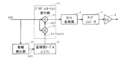
- FIG. 1 shows a configuration example of an amplifier with a predistorter according to an embodiment of the present invention.
- the amplifier with a predistorter in this example is provided in, for example, a transmitter of a base station apparatus.
- An amplifier with a predistorter in this example includes a predistorter (PD) 1, a D / A (Digital to Analog) converter 2, an up converter (frequency converter) 3, and a power amplifier (PA) 4.
- PD predistorter
- D / A Digital to Analog converter 2
- PA power amplifier
- a directional coupler 5 a down converter (frequency conversion unit) 6
- a / D (Analog to Digital) converter 7 an A / D (Analog to Digital) converter 7
- a feedback filter composed of, for example, a band-pass filter (BPF: Band Pass Filter). 8 and an antenna 9 are provided.
- BPF Band Pass Filter
- the amplifier with a predistorter of the present example includes a ⁇ 3 acquisition unit 15, a filter 16 configured by, for example, a band pass filter, a ⁇ 5 acquisition unit 17, and a filter 18 configured by, for example, a band pass filter.
- the feedback filter 8 and the input filters 16 and 18 all have the same filter characteristics, and have the characteristic of removing the frequency band of the input signal (desired signal). Yes. ⁇ 3 and ⁇ 5 will be described later.
- the predistorter 1 includes an amplitude detection unit 11, a distortion compensation table 12 made up of a LUT (Look Up Table) including a memory, a predistortion execution unit 13, and a control unit (learning unit) 14. Yes.
- LUT Look Up Table
- the predistorter 1 includes an amplitude detection unit 11, a distortion compensation table 12 made up of a LUT (Look Up Table) including a memory, a predistortion execution unit 13, and a control unit (learning unit) 14. Yes.
- An input signal (for example, a signal to be transmitted) to the amplifier with a predistorter is input to the predistorter 1 and input to the amplitude detecting unit 11 and the predistortion executing unit 13.
- An input signal to the amplifier with predistorter is also input to the ⁇ 3 acquisition unit 15 and the ⁇ 5 acquisition unit 17.
- the amplitude detector 11 detects the amplitude value of the input signal and outputs it to the distortion compensation table 12. This amplitude value is associated as a reference argument of the distortion compensation table 12.
- the distortion compensation table 12 stores a table for performing distortion compensation by a predistortion method.
- This table defines the inverse characteristic of the nonlinear characteristic of the amplifier to be compensated for distortion (in this example, the amplifier of the power amplifying unit 4), and generally AM-AM using the amplitude of the input signal as an index. It relates to characteristics (amplitude) and AM-PM characteristics (phase).
- the distortion compensation table 12 stores the correspondence between the amplitude value and the distortion compensation coefficient (control coefficient) to be supplied to the predistortion execution unit 13, and the amplitude input from the amplitude detection unit 11. Is output to the predistortion execution unit 13.
- the predistortion execution unit 13 gives the predistortion distortion to the input signal according to the distortion compensation coefficient (reference result of the distortion compensation table 12) input from the distortion compensation table 12, thereby adjusting the amplitude and phase of the input signal. Compensate and output the compensated signal to the D / A converter 2.
- the D / A converter 2 converts the signal input from the predistortion execution unit 13 from a digital signal to an analog signal and outputs the analog signal to the upconverter 3.
- the up-converter 3 converts the signal input from the D / A converter 2 into a radio frequency signal by frequency conversion (up-conversion) and outputs the signal to the power amplification unit 4.
- the power amplifying unit 4 amplifies and outputs the signal input from the up-converter 3. This output signal is transmitted from the antenna 9 by radio, for example.
- the signal amplified by the power amplifying unit 4 is a signal that has been preliminarily distorted by a reverse characteristic of the non-linear characteristic of the power amplifying unit 4 by a predistortion method. As a result, the output signal of the power amplifying unit 4 becomes a signal in which the distortion is compensated.
- the directional coupler 5 distributes a part of the output signal from the power amplifier 4, acquires it as a feedback signal, and outputs it to the down converter 6.
- the down converter 6 converts the feedback signal input from the directional coupler 5 into a baseband or intermediate frequency band signal by frequency conversion (downconversion), and outputs the signal to the A / D converter 7.
- the A / D converter 7 converts the signal input from the down converter 6 from an analog signal to a digital signal and outputs the signal to the control unit 14.
- the distortion component included in the feedback signal input to the control unit 14 via the down converter 6 and the A / D converter 7 is extracted based on the characteristics of the filter 8, and the signal of the distortion component is controlled. Used in part 14. Details of the filter 8 will be described later with reference to FIGS.
- the ⁇ 3 acquisition unit 15 acquires a signal of ⁇ 3 based on the input signal and outputs it to the filter 16. Specifically, the ⁇ 3 acquisition unit 15 acquires and outputs a signal (value) of the function
- the filter 16 band-limits the signal of ⁇ 3 input from the ⁇ 3 acquisition unit 15 and outputs the signal to the control unit 14.
- the ⁇ 5 acquisition unit 17 acquires a signal of ⁇ 5 based on the input signal and outputs it to the filter 18.
- the ⁇ 5 acquisition unit 17 acquires and outputs a signal (value) of the function
- the filter 18 limits the band of the ⁇ 5 signal input from the ⁇ 5 acquisition unit 17 and outputs the signal to the control unit 14.
- the control unit 14 Based on the signal input from the A / D converter 7 (the signal after passing through the filter 8) and the signals input from the filters 16 and 18, the control unit 14 performs distortion compensation by the predistortion execution unit 13 more.
- the stored contents of the distortion compensation table 12 (correspondence between the amplitude value and the distortion compensation coefficient in this example) are updated so as to be favorable. By this update, it is possible to adapt to, for example, temperature change or aging change.
- the control unit 14 performs complex multiplication on the signal of the distorted component fed back and the signal related to ⁇ 3 input from the filter 16, thereby obtaining the signal of the distorted component (the entire distorted component).
- the component corresponding to ⁇ 3 included is extracted, and the signal of the distortion component (whole distortion component) is obtained by complex multiplication of the signal of the distortion component fed back and the signal related to ⁇ 5 input from the filter 18.
- the component corresponding to ⁇ 5 included in the ⁇ 5 is extracted, and control is performed so that the distortion component corresponding to each ⁇ 3 , ⁇ 5 is reduced.
- processing units acquisition units 15 and 17 and filters 16 and 18
- ⁇ 3 and ⁇ A configuration including a processing unit related to only one of 5 or a configuration including a processing unit related to ⁇ i of 7th order or higher may be used.
- the control unit 14 when the processing unit is provided with about [Phi i, by a signal of the signal and the fed-back distortion component related to the [Phi i complex multiplication, the distortion components corresponding to the [Phi i It can be extracted and used for control.
- FIG. 2 shows a configuration example of the predistortion execution unit 13, and the peripheral processing units 2 to 4, 11, and 12 are also shown.
- the predistortion execution unit 13 of this example includes a complex multiplier 31 and a complex adder 32.
- the input signal x (t) is input to the complex multiplier 31 and the complex adder 32.
- the amplitude detector 11 detects the amplitude value
- the distortion compensation table 12 detects the distortion compensation coefficient LUT (
- the complex multiplier 31 performs complex multiplication on the input signal x (t) and the distortion compensation coefficient LUT (
- the complex adder 32 performs complex addition on the input signal x (t) and the complex multiplication result p (t), and outputs the complex addition result to the D / A converter 2.
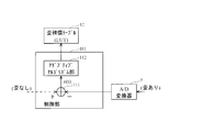
- FIG. 3 (a) shows a configuration example relating to the calculation of the control unit 14a (corresponding to the control unit 14 shown in FIG. 1) according to an embodiment of the present invention when an analog filter is used.
- a band pass filter (BPF) 71 having a characteristic of passing a signal outside the desired signal band, an A / D converter 7, a control unit 14 a including an adaptive algorithm unit 81, and a distortion compensation table 12 Is shown.
- the band-pass filter 71 corresponds to the filter 8 shown in FIG.
- an analog band-pass filter 71 is provided between the down converter 6 and the A / D converter 7 (preceding stage of the A / D converter 7).
- the output signal from the down converter 6 is filtered by the band pass filter 71 to extract a signal outside the desired signal band as an error signal e (t), and the extracted error signal e (t) is converted into an A / D converter.
- the adaptive algorithm unit 81 of the control unit 14a uses, for example, a coefficient for predistortion learning by a perturbation algorithm based on the error signal e (t) and the input signals from the filters 16 and 18. Details will be updated in an embodiment of the present invention (described later in [Description of Configuration of First Embodiment]).
- FIG. 3B shows a configuration example related to the calculation of the control unit 14b (corresponding to the control unit 14 shown in FIG. 1) according to an embodiment of the present invention when a digital filter is used.
- an A / D converter 7 a control unit 14 b including a band pass filter 91 having a characteristic of passing a signal outside the desired signal band and an adaptive algorithm unit 92, and the distortion compensation table 12 are shown.
- the band-pass filter 91 corresponds to the filter 8 shown in FIG.
- a band pass filter 91 that performs digital calculation is provided inside the control unit 14b (after the A / D converter 7). Then, in the control unit 14b, a signal outside the desired signal band is extracted as an error signal e (t) by filtering the input signal from the A / D converter 7 by the band pass filter 91, and the extracted error signal e ( t) and the adaptive algorithm unit 92 based on the input signals from the filters 16 and 18, for example, a predistortion learning coefficient (for details, refer to the embodiment of the present invention (refer to [the first embodiment In the explanation of the configuration] and later)), the following will be updated.
- a predistortion learning coefficient for details, refer to the embodiment of the present invention (refer to [the first embodiment In the explanation of the configuration] and later)
- band pass filters 71 and 91 are used as a filter
- a band limiting filter having similar filtering characteristics can be used as another configuration example.
- the band limiting filter for example, an FIR (Finite Impulse Response) filter or the like is usually used.
- the effect obtained by the configuration of this example shown in FIGS. 3A and 3B will be described with respect to the configuration of the background art shown in FIG.
- the power level of the frequency of the distortion component included in the feedback signal is viewed as the error signal e (t), and the gain (Gain) and phase (time ⁇ ) of the feedback signal are If it does not match the original signal, an error occurs, so level adjustment is necessary.
- signal components other than the desired wave are obtained by the band pass filters 71 and 91 using only the feedback signal.
- an error signal for example, an error vector in the time domain of the distortion band
- the signal obtained by attenuating or removing the desired signal from the output signal of the amplifier (in this example, the amplifier of the power amplification unit 4) using the bandpass filters 71 and 91.
- the bandpass filters 71 and 91 Is used as an error signal e (t) to learn a coefficient for learning predistortion. Therefore, in the amplifier with a predistorter of this example, the signal from which the desired signal band is removed by the bandpass filters 71 and 91 is used as the error signal e (t). (Computation) becomes unnecessary, the circuit scale can be reduced, and the convergence time is shortened by the simplification of the processing.
- the distortion compensation coefficient for example, the content of the distortion compensation table 12 that defines the distortion compensation coefficient
- FIG. 4 shows a configuration example of a memoryless predistorter using power series expansion as a reference.
- the memoryless predistorter of the present example is the one corresponding to the predistorter 1 shown in FIG.
- the memoryless predistorter of this example includes a square detection unit 21, a multiplier 22, and a complex multiplier 23 as a processing unit related to the third-order term, and as a processing unit related to the fifth-order term, A fourth power detection unit 24, a multiplier 25, and a complex multiplier 26 are provided, and a similar processing unit (not shown) is also provided for each odd-order term after the seventh order.
- a processing unit up to any practically effective order (arbitrary odd order of 3rd order or higher) may be provided.
- the memoryless predistorter of this example includes an adder 27 as a processing unit common to all orders.
- the input signal is a complex signal.
- the square detection unit 21 detects (for example, calculates) the square value of the input signal, and the multiplier 22 multiplies the square value and the input signal.
- the amplitude of the input signal is the third power, and the phase is maintained.
- the complex multiplier 23 performs complex multiplication of the signal of the multiplication result and the predistorter coefficient ⁇ 3 .
- the pre-disc coefficients distorter alpha 3 is a complex number, (in FIG. 4, not shown) the control unit is set to be able to compensate for distortion.
- the fourth power detection unit 24 detects (for example, calculates) the fourth power value of the input signal, and the multiplier 25 multiplies the fourth power value and the input signal. In the signal resulting from the multiplication, the amplitude of the input signal is the fifth power and the phase is maintained. Then, complex multiplier 26 performs a complex multiplication of the coefficient alpha 5 signal and the predistorter of the multiplication result.
- the coefficient alpha 5 in the predistorter is a complex number, (in FIG. 4, not shown) the control unit is set to be able to compensate for distortion.
- the adder 27 inputs and adds (sums) the signals and input signals output from the processing systems (complex multipliers 23, 26,...) Of all odd-order terms, and the addition result is obtained.
- the signal is output as a signal after the predistortion process (in FIG. 1, to the D / A converter 2).
- the input signal x (t) is a complex signal.
- the amplitude detector 11 calculates the amplitude value
- is expressed as (Equation 6).
- the signal p (t) added to the input signal x (t) is generally expressed as (Equation 7).
- ⁇ i is a coefficient of the predistorter and is a complex number.
- Equation 7) is expressed by a power series like (Equation 1), and the nonlinear distortion component of (Equation 1) can be compensated by appropriately selecting ⁇ i .
- the distortion compensation table (LUT) 12 composed of a memory or the like stores data as shown in (Equation 8) by the control unit 14.
- the input signal z (t) of the amplifier is a signal obtained by adding the predistortion signal p (t) shown in (Expression 10) to the input signal x (t), and is expressed as (Expression 11).
- the first term on the right side of (Equation 13) represents the amplified desired signal.
- the second term on the right side represents the third-order distortion component, and ⁇ 3 is determined so that the distortion is compensated. It can be seen that in the third to fifth terms on the right side, new fifth-order components, seventh-order components, and ninth-order components are generated.
- Equation (10) the degree the higher order predistorter (fifth, seventh, 8) when considering also the third order pre-disc coefficients distorter alpha 3, 5-order coefficient alpha 5 or the predistorter coefficients and alpha 7 of 7 next predistorter, to affect such factors alpha 9 of 9 order predistorter, alpha 5 in accordance with the values of alpha 3, alpha 7 , optimal values such as ⁇ 9 will change.
- the conventional method has a problem that it takes a long time to adaptively converge the coefficients ( ⁇ 3 , ⁇ 5 , ⁇ 7, etc.) of the memoryless predistorter.
- Equation 9 the order of the nonlinear component of the amplifier is taken into consideration up to the third order.
- higher orders such as the fifth order, the seventh order,. Will affect the coefficient.
- an orthogonal polynomial is introduced and used as a generation polynomial of the inverse characteristic of the nonlinear characteristic.
- orthogonal polynomials are used to make a plurality of predistorter generator polynomials orthogonal, thereby making the coefficients independent so that the convergence time is shortened. An example is shown below.
- (Expression 7) described above is expressed as (Expression 14) and (Expression 15).
- a i represents a coefficient for predistortion learning
- ⁇ ij which is a parameter (orthogonalization coefficient) for orthogonalization
- N is an odd number.
- each ⁇ ( ⁇ 3 to ⁇ N ) shown in (Equation 15) is orthogonal.
- the function E [•] is defined as in (Equation 17).
- the time T of the above-described time (0 to T) is the time length of data used for one update, and in general, the longer the time, the smaller the error, so that it is ideally infinite. However, in practice, any value may be used to the extent that is practically effective.
- different signals are orthogonalized each time, so that the length of the amplitude of the input signal sufficient for orthogonalization is obtained (or more). For example, a length (or more) of time that can obtain a probability density as high as that of the original signal can be used.
- Equation 16 can be satisfied by appropriately selecting each ⁇ ij in the above (Equation 15).
- the value of the parameter ⁇ ij varies depending on the input signal x (t) at the time (0 to T) described above. Hereinafter, it is represented by a function of E [•].
- two cases are shown, ie, the case of ⁇ 3 shown in (Expression 18) and the case of ⁇ 5 shown in (Expression 19).
- equations such as (Expression 20), (Expression 21), and (Expression 22) are established.
- This example is applied to an amplifier with a predistorter in this example.
- the coefficient A i for predistortion learning has no effect other than ⁇ i , that is, it is obtained independently from the coefficient A j (i ⁇ j) for learning other predistortion. And therefore the convergence time is shortened. Specifically, for example, the number of updates until the content of the distortion compensation table 12 converges from an initial state (for example, a state where there is no information) is reduced.
- the predistortion learning for adapting by using the orthogonal polynomial is performed. Since the coefficients are orthogonal, the convergence time of the distortion compensation table 12 can be shortened and efficiency can be improved.
- FIG. 13 shows a filter on the input side (corresponding to the filters 16 and 18 shown in FIG. 1) and a feedback filter (FIG. 1) as in the configuration of the amplifier with predistorter shown in FIG.
- E [ ⁇ m * ⁇ ⁇ n ] is shown as a case where the filter 8 corresponding to the filter 8 shown in FIG. .
- W-CDMA Wideband-Code Division Multiple Access
- a i is a distortion compensation coefficient (a coefficient for learning predistortion).
- ⁇ ij is a parameter (orthogonalization coefficient) for orthogonalizing the orthogonal function ⁇ i .
- the signal components ⁇ 3 * , ⁇ 5 * , and ⁇ 7 * of the input side (transmission side) are shown in the row (vertical direction), and the input side as shown in FIG. In this case, the filters 16 and 18 are not provided.
- components ( ⁇ 3 , ⁇ 5 , ⁇ 7 ) of the error signal on the feedback side are shown in the row (lateral direction), and the case where the filter 8 on the feedback side as shown in FIG. 1 is not provided is shown. is there.
- FIG. 13 it was confirmed that when an error signal is obtained by ideally adjusting the level, delay time, etc. between the transmission signal and the feedback signal, they are completely orthogonal.
- FIG. 14 includes a feedback filter (corresponding to the filter 8 shown in FIG. 1) as in the configuration of the amplifier with a predistorter shown in FIG.
- An example of E [ ⁇ m * ⁇ ⁇ n ] is shown for a case where the filter (corresponding to the filters 16 and 18 shown in FIG. 1) is not provided. Note that a W-CDMA signal is used as a transmission signal.
- a i is a distortion compensation coefficient (a coefficient for learning predistortion).
- ⁇ ij is a parameter (orthogonalization coefficient) for orthogonalizing the orthogonal function ⁇ i .
- the components ( ⁇ 3 * , ⁇ 5 * , ⁇ 7 * ) of the signal on the input side (transmission side) are shown in the row (vertical direction), and the input side as shown in FIG. In this case, the filters 16 and 18 are not provided.
- components ( ⁇ 3 , ⁇ 5 , ⁇ 7 ) of the error signal on the feedback side are shown in the column (horizontal direction), and the case where the filter 8 on the feedback side as shown in FIG. 1 is provided is shown. is there.
- the orthogonality was found to be quite lost. Therefore, there is still room for improvement in the method for shortening the convergence time and reducing the hardware scale, and further effective method development is expected.
- Equation 30 an orthogonal polynomial in which the desired signal band is suppressed by BPF is defined as (Equation 30).
- BPF [] represents a signal in which the desired signal band is suppressed.
- the orthogonalization coefficient ⁇ ij that is a parameter is calculated using (Expression 30) instead of (Expression 15) described above.
- the same method as that in the case of using (Expression 15) described above can be used.
- (Equation 31) holds.
- the method using (Equation 30) in this example is different from (Equation 32). Therefore, different orthogonalization coefficients ⁇ ij are obtained.
- the orthogonalization coefficient ⁇ ij which is a parameter is obtained from the input signal x (t). Specifically, it is obtained using a sufficiently long signal having general signal characteristics (for example, characteristics such as CDMA and OFDM (Orthogonal Frequency Division Multiplexing)).
- the orthogonalization coefficient ⁇ ij that is a parameter is fixed and constant when it is first obtained by, for example, computer simulation using (Equation 30).
- each orthogonal function (PHI) i is calculated
- the orthogonal function ⁇ i varies according to the input signal x (t), and varies with time on both the input side and the feedback side (distortion component).
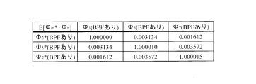
- FIG. 5 shows a case where the orthogonalization coefficient ⁇ ij of the orthogonal polynomial is calculated using (Equation 30) of the present example, and a feedback system filter like the configuration of the amplifier with a predistorter shown in FIG.
- An example of E [ ⁇ m * ⁇ ⁇ n ] is shown for the case where both the 8 and the filters 16 and 18 on the input side are provided. Note that a W-CDMA signal is used as a transmission signal.
- the components ( ⁇ 3 * , ⁇ 5 * , ⁇ 7 * ) of the signal on the input side (transmission side) are shown in the row (vertical direction), and the input side as shown in FIG. In this case, the filters 16 and 18 are provided. Further, components ( ⁇ 3 , ⁇ 5 , ⁇ 7 ) of the error signal on the feedback side are shown in the column (horizontal direction), and the case where the filter 8 on the feedback side as shown in FIG. 1 is provided is shown. is there. In the case of this example shown in FIG. 5, although it is not completely orthogonal, it was confirmed that the orthogonality is large compared to the case of FIG. 14 described above in which (Equation 30) of this example is not applied.
- the predistorter-equipped amplifier uses the orthogonalization coefficient ⁇ ij of the orthogonal polynomial obtained by raising the amplitude of the transmission signal to a power and using the band-limited signal of the raised signal.
- the orthogonalization coefficient ⁇ ij of the orthogonal polynomial is calculated using (Equation 30) as in this example, for example, compared to the case where the orthogonalization coefficient ⁇ ij of the orthogonal polynomial is calculated using (Equation 15).
- the convergence time can be shortened to increase efficiency.
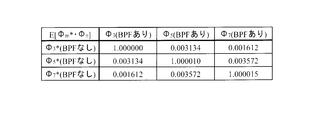
- FIG. 6 shows a case where the orthogonalization coefficient ⁇ ij of the orthogonal polynomial is calculated using (Equation 30) of the present example, and a feedback system filter like the configuration of the amplifier with predistorter shown in FIG. 8 shows an example of E [ ⁇ m * ⁇ ⁇ n ] in the case where the input side filters 16 and 18 are not provided. Note that a W-CDMA signal is used as a transmission signal.
- the components ( ⁇ 3 * , ⁇ 5 * , ⁇ 7 * ) of the signal on the input side (transmission side) are shown in the row (vertical direction), and the input side as shown in FIG. In this case, the filters 16 and 18 are not provided. Further, components ( ⁇ 3 , ⁇ 5 , ⁇ 7 ) of the error signal on the feedback side are shown in the column (horizontal direction), and the case where the filter 8 on the feedback side as shown in FIG. 1 is provided is shown. is there.
- the values in the table shown in FIG. 5 and the values in the table shown in FIG. 6 are exactly the same, and it was confirmed that the same orthogonal effect can be obtained.
- E [ ⁇ m * ⁇ ⁇ n ] is convolution in the time domain, it is multiplied in the frequency domain. Then, one side (here, the feedback side) is removed by a band-limiting filter, that is, multiplied by 0.0, so that the result is the same.
- the amplifier with a predistorter of this example when the amplitude of the transmission signal is raised to the power, and the orthogonalization coefficient ⁇ ij of the orthogonal polynomial obtained using the band-limited signal of the raised signal is used, It is possible to adopt a configuration in which the adaptive coefficient is learned by not performing band limitation on the side signal (transmission signal) and performing band limitation on the feedback signal. In such a configuration, every time the coefficient for predistortion learning is updated, the bandwidth of the data of T [sec] (data acquisition time used for one update, which is an arbitrary value) time is limited. Is not necessary, and the processing can be simplified.
- T [sec] data acquisition time used for one update, which is an arbitrary value
- Equation 7 shows, in this example the case of calculating the tap coefficients phi ij of orthogonal polynomials using (Equation 30) (the proposed method), the orthogonalization coefficient phi ij of orthogonal polynomials using (Equation 15)
- An example of the convergence process of ACLR is shown for the case of calculation (comparison method).
- the horizontal axis represents the number of updates [times], and the vertical axis represents ACLR [dBc].
- the convergence time is compared between the proposed method and the comparison method, it is confirmed that the proposed method converges to a good ACLR in about 100 times compared to about 500 times in the comparison method.
- the proposed method when a filter for band limitation is used for the feedback signal, the orthogonality of each coefficient increases, that is, it is possible to converge independently, so that the convergence time is shortened. The effect is appearing.
- a signal in which a desired signal band is suppressed by a filter (BPF in this example) is used to calculate the orthogonalization coefficient ⁇ ij .
- band limitation is performed using a filter (BPF in this example) on both the input side and the feedback side.
- a feedback signal corresponding to the error signal e (t) is filtered (in this example, , BPF), the desired signal is removed and the orthogonal function ⁇ i of the orthogonal polynomial on the input side (transmission side) for correlation with the desired signal is not subjected to band limitation, thereby simplifying the processing.
- the filter in this example, BPF
- the filter is to calculate the tap coefficients phi ij of orthogonal polynomials using Considering Equation (30), a BPF for others
- a BPF for others
- the same processing as when not considered is performed, for example, each ⁇ i component signal acquisition processing by the ⁇ i acquisition unit (in this example, ⁇ 3 acquisition unit 15 or ⁇ 5 acquisition unit 17), the control unit 14 or distortion
- the predistortion control processing by the compensation table 12 and the predistortion execution unit 13 is performed based on (Equation 15).
- a second embodiment of the present invention will be described.
- a memory effect predistorter In this example, a case where a memory effect predistorter is used will be described.
- compensation for the memory effect is important as well as compensation for AM-AM conversion and AM-PM conversion.
- the baseband even-order distortion component remodulates the input signal by changing the power supply voltage via the impedance of the power supply circuit, and compensates for the memory effect that newly generates an in-band odd-order component.
- a predistorter is shown.
- FIG. 8 shows a configuration example of a memory effect predistorter using power series expansion as a reference.
- the memory effect predistorter of the present example is a principle configuration example corresponding to the predistorter 1 shown in FIG.
- the memory effect predistorter of this example includes a square detection unit 41, a delay circuit 42, a subtractor 43, a multiplier 44, and a complex multiplier 45 as a processing unit related to the second-order term.
- the fourth-order term processing unit includes a fourth power detection unit 46, a delay circuit 47, a subtractor 48, a multiplier 49, and a complex multiplier 50, and each even number after the sixth order.
- a similar processing unit (not shown) is provided for the next item.
- a processing unit up to any practically effective order any even order greater than or equal to the second order may be provided.
- the memory effect predistorter of this example includes an adder 51 as a processing unit common to all orders.
- the input signal is a complex digital baseband signal.
- the square detection unit 41 detects (for example, calculates) the square value of the input signal to the predistorter, and the delay circuit 42 outputs the output from the square detection unit 41 (2 (Multiplier value) is delayed by U [sec] (preferably 1 clock time).
- the subtractor 43 subtracts the output (square value) of the square detection unit 41 before U [sec] from the output (square value) of the square detection unit 41. Thereby, the output from the subtracter 43 becomes a difference of square values.
- the multiplier 44 multiplies the difference value of the square value by the input signal.
- the output signal of the multiplication result corresponds to a signal obtained by remodulating the carrier signal, and becomes a third-order component and has a frequency component near the carrier frequency.
- Complex multiplier 45 multiplies the coefficient beta 2 predistorter output signal from the multiplier 44.
- the coefficient ⁇ 2 of the predistorter is a complex number and is set so that the control unit (not shown in FIG. 8) can compensate for the distortion.
- the fourth power detection unit 46 detects (for example, calculates) the fourth power value of the input signal to the predistorter, and the delay circuit 47 outputs the output from the fourth power detection unit 46 (4 (Multiplier value) is delayed by U [sec] (preferably 1 clock time).
- the subtracter 48 subtracts the output (fourth power value) of the fourth power detection unit 46 before U [sec] from the output (fourth power value) of the fourth power detection unit 46. Thereby, the output from the subtracter 48 becomes a difference of the fourth power value.
- the multiplier 49 multiplies the difference value of the fourth power value by the input signal.
- the output signal of the multiplication result corresponds to a signal obtained by remodulating the carrier signal, and becomes a fifth-order component and has a frequency component near the carrier frequency.
- the complex multiplier 50 multiplies the output signal from the multiplier 49 by the coefficient ⁇ 4 of the predistorter.
- the coefficient ⁇ 4 of the predistorter is a complex number and is set so that the control unit (not shown in FIG. 8) can compensate for the distortion.
- the adder 51 inputs and adds (sums) the signals and input signals output from the processing systems (complex multipliers 45, 50,...) Of all even-order terms, and the addition result is obtained.
- the signal is output as a signal after the predistortion process (in FIG. 1, to the D / A converter 2).
- U [sec] for example, a value of (1 clock time ⁇ an integer equal to or greater than 1) can be used.
- an orthogonal polynomial is introduced and used as a generation polynomial of the inverse characteristic of the memory effect characteristic.
- orthogonal polynomials are used to make a plurality of predistorter generator polynomials orthogonal, thereby making the coefficients independent so that the convergence time is shortened. An example is shown below.
- the orthogonalization coefficient ⁇ ij as a parameter is a real number, and M is an even number.
- each ⁇ ( ⁇ 2 to ⁇ M ) are orthogonal.
- two cases of ⁇ 2 and ⁇ 4 are shown.
- the three equations shown in (Equation 36) can be formed, so that the AM-AM conversion and the AM-PM conversion according to the first embodiment are compensated. It can be solved in the same way as the predistorter.
- the predistortion is learned by using the orthogonal polynomial. Since the coefficients are orthogonal, the convergence time of the distortion compensation table 12 can be shortened, and the efficiency can be improved.
- an orthogonal polynomial is used in a predistorter that compensates for the memory effect using a difference signal between a signal obtained by multiplying an input signal by an even power and a signal obtained by delaying the even power signal.
- a signal in which a desired signal band is suppressed by a filter composed of, for example, a BPF is used.
- this filter is a BPF.
- the characteristics of this filter are the same as the characteristics of the feedback filter 8 and the filters 16 and 18 on the input side, and all these filters have the same filter characteristics.
- the orders handled are second order, fourth order, sixth order,..., M order (M is an even number).
- M is an even number.
- an orthogonal polynomial in which the desired signal band is suppressed by the BPF is defined as (Equation 37).
- BPF [] represents a signal in which the desired signal band is suppressed.
- the orthogonal each ⁇ 2 ⁇ ⁇ M shown in (Equation 37).
- the orthogonalization coefficient ⁇ ij that is a parameter is calculated using (Expression 37) instead of (Expression 35) described above.
- a calculation method a method similar to the case of using (Expression 35) described above can be used.
- the orthogonalization coefficient ⁇ ij which is a parameter is obtained from the input signal x (t). Specifically, it is obtained using a sufficiently long signal having general signal characteristics (for example, characteristics such as CDMA and OFDM).
- the orthogonalization coefficient ⁇ ij that is a parameter is fixed and constant when it is first obtained by, for example, computer simulation using (Equation 37).
- each orthogonal function (PHI) i is calculated
- the orthogonal function ⁇ i varies according to the input signal x (t), and varies with time on both the input side and the feedback side (distortion component).
- the predistorter-equipped amplifier of this example uses the orthogonalization coefficient ⁇ ij of the orthogonal polynomial obtained by using the signal obtained by, for example, raising the amplitude of the transmission signal to the power and band-limiting the signal obtained by the power.
- the orthogonalization coefficient ⁇ ij of the orthogonal polynomial is calculated using (Expression 37) as in this example, for example, compared with the case where the orthogonalization coefficient ⁇ ij of the orthogonal polynomial is calculated using (Expression 35).
- the convergence time can be shortened to increase efficiency.
- the amplifier with a predistorter when the amplitude of the transmission signal is raised to the power, and the orthogonalization coefficient ⁇ ij of the orthogonal polynomial obtained using the band-limited signal of the raised signal is used. It is possible to adopt a configuration in which the adaptive coefficient is learned by performing band limitation on the feedback signal without performing band limitation on the input-side signal (transmission signal). In such a configuration, every time the coefficient for predistortion learning is updated, the bandwidth of the data of T [sec] (data acquisition time used for one update, which is an arbitrary value) time is limited. Is not necessary, and the processing can be simplified.
- T [sec] data acquisition time used for one update, which is an arbitrary value
- a signal in which a desired signal band is suppressed by a filter (BPF in this example) is used to calculate the orthogonalization coefficient ⁇ ij .
- band limitation is performed using a filter (BPF in this example) on both the input side and the feedback side.
- the feedback signal corresponding to error signal e (t) filter in this example , BPF
- the desired signal is removed and the orthogonal function ⁇ i of the orthogonal polynomial on the input side (transmission side) for correlation with the desired signal is not subjected to band limitation, thereby simplifying the processing.
- a configuration using an orthogonal polynomial or a configuration for calculating the orthogonalization coefficient ⁇ ij of the orthogonal polynomial using the above-described (Expression 37) using a filter (BPF in this example) is roughly as follows. Since the processing is the same as that described in the first embodiment, the same processing as that described in the first embodiment can be applied to the detailed processing.
- FIG. 9 shows a configuration example of a predistorter according to an embodiment of the present invention.
- AM-AM conversion and AM-PM conversion are compensated, and the memory effect is compensated.
- the predistorter of this example includes a memoryless predistorter (memoryless PD) 61, a memory effect predistorter (memory effect PD) 62, an adder 63, and an adder 64.
- a memoryless PD 61 and a memory effect PD 62 are provided in parallel.
- the memoryless PD 61 one having a principle configuration as shown in FIG. 4 can be used
- the memory effect PD 62 one having a principle configuration as shown in FIG. 8 is used. Can do.
- the memoryless PD 61 compensates for AM-AM conversion and AM-PM conversion for the input signal to the predistorter, and the memory effect PD62 for the input signal to the predistorter
- the adder 63 adds both of these compensated signals
- the adder 64 adds the signal p (t) of the addition result and the input signal to the predistorter to obtain the result of the addition. Output a signal.
- the memoryless PD 61 and the memory effect PD 62 are separate processing units, and have different distortion compensation tables (similar to the distortion compensation table 12 shown in FIG. 1).
- the memoryless PD 61 and the memory effect PD 62 correspond to the predistorter 1 shown in FIG. 1, respectively.
- the memoryless PD adder 27 shown in FIG. 4 and the memory effect shown in FIG. It can be understood that the PD adder 51 is shared to form the adder 64 shown in FIG.
- an orthogonal polynomial is introduced and used as a generating polynomial for the inverse characteristic of the nonlinear characteristic.
- orthogonal polynomials are used to make a plurality of predistorter generator polynomials orthogonal, thereby making the coefficients independent so that the convergence time is shortened.
- the adaptation is performed by using the orthogonal polynomial. Since the coefficients for predistortion learning are orthogonal, the convergence time of the distortion compensation table can be shortened and efficiency can be improved.
- a predistorter in which a memoryless predistorter and a memory effect predistorter are connected in parallel, by learning the adaptive coefficients of both predistorters using orthogonal polynomials, The coefficients of both the memoryless predistorter and the memory effect predistorter can be made orthogonal to adapt quickly.
- a signal in which a desired signal band is suppressed by a filter composed of, for example, a BPF is used.
- this filter is a BPF.
- the characteristics of this filter are the same as the characteristics of the feedback filter 8 and the filters 16 and 18 on the input side, and all these filters have the same filter characteristics.
- the orders handled are the third order, fifth order, seventh order,..., N order (N is an odd number) and 2 orders.
- an orthogonal polynomial in which the desired signal band is suppressed by the BPF is defined as (Equation 42).
- BPF [] represents a signal in which the desired signal band is suppressed.
- each ⁇ i shown in (Equation 42) is orthogonal.
- the orthogonalization coefficient ⁇ ij that is a parameter is calculated using (Expression 42) instead of (Expression 40) described above.
- the same method as that in the case of using (Equation 40) described above can be used.
- the orthogonalization coefficient ⁇ ij which is a parameter is obtained from the input signal x (t). Specifically, it is obtained using a sufficiently long signal having general signal characteristics (for example, characteristics such as CDMA and OFDM).
- the orthogonalization coefficient ⁇ ij as a parameter is fixed and constant when it is first obtained by, for example, computer simulation using (Equation 42).
- each orthogonal function (PHI) i is calculated
- the orthogonal function ⁇ i varies according to the input signal x (t), and varies with time on both the input side and the feedback side (distortion component).
- the predistorter-equipped amplifier of this example uses the orthogonalization coefficient ⁇ ij of the orthogonal polynomial obtained by using the signal obtained by, for example, raising the amplitude of the transmission signal to the power and band-limiting the signal obtained by the power.
- the orthogonalization coefficient ⁇ ij of the orthogonal polynomial is calculated using (Expression 42) as in this example, for example, compared with the case where the orthogonalization coefficient ⁇ ij of the orthogonal polynomial is calculated using (Expression 40).
- the convergence time can be shortened to increase efficiency.
- the amplifier with a predistorter when the amplitude of the transmission signal is raised to the power, and the orthogonalization coefficient ⁇ ij of the orthogonal polynomial obtained using the band-limited signal of the raised signal is used. It is possible to adopt a configuration in which the adaptive coefficient is learned by performing band limitation on the feedback signal without performing band limitation on the input-side signal (transmission signal). In such a configuration, every time the coefficient for predistortion learning is updated, the bandwidth of the data of T [sec] (data acquisition time used for one update, which is an arbitrary value) time is limited. Is not necessary, and the processing can be simplified.
- T [sec] data acquisition time used for one update, which is an arbitrary value
- a signal in which a desired signal band is suppressed by a filter (BPF in this example) is used to calculate the orthogonalization coefficient ⁇ ij .
- band limitation is performed using a filter (BPF in this example) on both the input side and the feedback side.
- a configuration using an orthogonal polynomial or a configuration for calculating the orthogonalization coefficient ⁇ ij of the orthogonal polynomial using the above-described (Equation 42) using a filter (BPF in this example) is roughly as follows. Since it is the same as that described in the first embodiment and the second embodiment described above, detailed processing is the same as that described in the first embodiment and the second embodiment described above. It is possible to apply.
- the amplitude detector 11 may be provided independently or in common, and the distortion compensation table 12 or The predistortion execution unit 13 is provided independently, and the control unit 14 and the feedback system (directional coupler 5, down converter 6, A / D converter 7) are provided in common.
- the ⁇ i acquisition unit in this example, the ⁇ 3 acquisition unit 15 and the ⁇ 5 acquisition unit 17
- the filters 16 and 18 on the input side are provided in common and the filter 8 on the feedback side is also provided in common.
- FIG. 10 shows another configuration example of an amplifier with a predistorter according to an embodiment of the present invention.
- the configuration and operation of the amplifier with a predistorter of this example are, for example, ⁇ 3 acquisition unit 15, filter 16, ⁇ 5 acquisition unit 17, filter compared with the configuration and operation of the amplifier with predistorter shown in FIG. 18 is different in that 18 is not provided.
- the control unit 14 receives the signal input from the A / D converter 7. Based on (the signal after passing through the filter 8), the stored contents of the distortion compensation table 12 (in this example, the amplitude value and the distortion compensation coefficient are set so that the distortion compensation by the predistortion execution unit 13 becomes better. Update). By this update, it is possible to adapt to, for example, temperature change or aging change. In this case, the control unit 14 performs control so as to reduce it based on the signal of the fed back distortion component (the entire distortion component).
- the distortion component signal is extracted by the filter 8 provided in the feedback system in either the configuration of the amplifier with the predistorter as shown in FIG. 1 or the configuration of the amplifier with the predistorter as shown in FIG. Then, control can be performed so that it becomes smaller. Therefore, in the first to third embodiments described above, the case where the amplifier with the predistorter shown in FIG. 1 is used is shown. Instead, the amplifier with the predistorter shown in FIG. 10 is used. In other words, the amplifier with a predistorter shown in FIG. 10 uses a signal in which a desired signal band is suppressed by a filter (BPF in this example) for calculation of the orthogonalization coefficient ⁇ ij. It is also possible to do.
- BPF filter
- the level detection means is configured by the function of the amplitude detector 11, and a distortion compensation table (LUT) is provided.
- Corresponding storage means is constituted by the function of 12
- predistortion execution means is constituted by the function of the predistortion execution part 13
- filter means is constituted by the function of the filter 8
- the control part (learning) 14 function is configured corresponding acquisition means by the input signal function value acquiring unit by the function of [Phi 3 acquisition unit 15 and [Phi 5 acquisition unit 17 is configured.
- the coefficient ⁇ i may be of only one type), and the correspondence between the level of the signal input to the predistorter and the distortion compensation coefficient for performing predistortion is a distortion compensation table (LUT).
- ) 12 is the contents of the table written in 12
- the orthogonal polynomial is a group of ⁇ 1 , ⁇ 2 , ⁇ 3 , ⁇ 4 , ⁇ 5 ,...
- each orthogonal function is ⁇ 1 , ⁇ 2 , ⁇ 3 , ⁇ 4 , ⁇ 5 ,...
- the parameter (for orthogonalization) is the orthogonalization coefficient ⁇ , specifically, ⁇ 33 , ⁇ 53 , ⁇ 55 , ⁇ 73 ,...
- the input signal function is
- the function obtained by filtering is BPF [
- a configuration example of the distortion compensation amplifying apparatus grasped from the embodiment described above A configuration example of the distortion compensation amplifying apparatus grasped from the embodiment described above will be shown.
- a first configuration example is a distortion compensation amplifying apparatus having a predistorter that generates a signal having an inverse characteristic of the nonlinear characteristic and outputs the signal to the amplifier in order to compensate for distortion generated by the nonlinear characteristic of the amplifier.
- Level detection means for detecting the level of a signal input to the predistorter;
- Correspondence storage means for storing a correspondence between a level of a signal input to the predistorter and a distortion compensation coefficient for performing predistortion;
- Predistortion execution means for giving an inverse characteristic of the nonlinear characteristic of the amplifier based on a distortion compensation coefficient for executing the predistortion on a signal input to the predistorter, and outputting the inverse characteristic to the amplifier;
- Filter means for removing a desired wave frequency component from the feedback signal of the amplifier output and outputting a distortion signal component;
- a coefficient for learning predistortion that constitutes a function that gives an inverse characteristic of the nonlinear characteristic of the amplifier to the signal input to the predistorter so that the distortion signal component acquired by the filter means becomes small
- the correspondence between the level of the signal input to the predistorter and the distortion compensation coefficient for executing the predistortion is obtained based on the
- Correspondence acquisition means for outputting to the storage means An orthogonal polynomial is used for the function that gives the inverse characteristic of the nonlinear characteristic of the amplifier,
- Each orthogonal function constituting the orthogonal polynomial is a sum of products of one or more input signal functions and parameters corresponding to the input signal functions,
- the values of the parameters respectively corresponding to the one or more input signal functions are obtained by applying a filter having the same filter characteristics as the filter means to the function of the input signal to constitute each orthogonal function.
- the orthogonal functions are set to be orthogonal to each other. This is a distortion compensation amplifying apparatus.
- the second configuration example is the distortion compensation amplification device of the first configuration example.
- the correspondence acquisition unit corresponds to each of the one or more orthogonal functions from the distortion signal component by performing complex multiplication of the signal acquired by the function signal acquisition unit and the distortion signal component acquired by the filter unit. Extracting a signal component and updating a coefficient for learning the predistortion so that it becomes smaller for each extracted signal component; This is a distortion compensation amplifying apparatus.
- the third configuration example is the distortion compensation amplifying apparatus of the first configuration example.
- Function signal acquisition means for acquiring signals obtained by functions of the input signals constituting the orthogonal functions based on signals input to the predistorter
- Function signal filtering means for obtaining a signal obtained by applying a filter having the same filter characteristics as the filter means to the signal obtained by the function signal obtaining means
- the correspondence acquisition unit corresponds to each of the one or more orthogonal functions from the distortion signal component by performing complex multiplication of the signal acquired by the function signal filter unit and the distortion signal component acquired by the filter unit. Extracting a signal component and updating a coefficient for learning the predistortion so that it becomes smaller for each extracted signal component; This is a distortion compensation amplifying apparatus.
- the third configuration example is a configuration example in which a filter is provided on the input signal side ( ⁇ ) in the second configuration example.
- the fourth configuration example is the distortion compensation amplifying apparatus of the first configuration example.
- the correspondence acquisition unit uses only the distortion signal component acquired by the filter unit, and updates the coefficient for learning the predistortion so that the entire distortion signal component becomes small. This is a distortion compensation amplifying apparatus.
- the level detection unit is configured by the function of the amplitude detection unit 11
- the correspondence storage unit is configured by the function of the distortion compensation table (LUT) 12
- the predistortion execution unit 13 is configured predistortion executing means by the function is configured the filter means by the function of the filter 8
- the control unit is configured corresponding acquisition unit by the function of (learning) 14
- a function signal acquisition means (means corresponding to the input signal function value acquisition means described above) is configured by the function of the 5 acquisition unit 17, and a function signal filter means is configured by the functions of the filter 16 and the filter 18.
- the number ⁇ i and the coefficient ⁇ i may be only one
- the correspondence between the level of the signal input to the predistorter and the distortion compensation coefficient for performing predistortion is distortion. It is the contents of the table written in the compensation table (LUT) 12, and the orthogonal polynomial is a group of ⁇ 1 , ⁇ 2 , ⁇ 3 , ⁇ 4 , ⁇ 5 ,.
- a parameter (for orthogonalization) is an orthogonalization coefficient ⁇ , and specifically Are ⁇ 33 , ⁇ 53 , ⁇ 55 , ⁇ 73 ,...
- the function of the input signal is
- the function obtained by filtering is BPF [
- the configuration of the system and apparatus according to the present invention is not necessarily limited to the configuration described above, and various configurations may be used.
- the present invention can also be provided as, for example, a method or method for executing the processing according to the present invention, a program for realizing such a method or method, or a recording medium for recording the program. It is also possible to provide various systems and devices.
- the application field of the present invention is not necessarily limited to the above-described fields, and the present invention can be applied to various fields.
- the processor executes a control program stored in a ROM (Read Only Memory) in hardware resources including a processor and a memory.
- ROM Read Only Memory
- a controlled configuration may be used, and for example, each functional unit for executing the processing may be configured as an independent hardware circuit.
- the present invention can be grasped as a computer-readable recording medium such as a floppy (registered trademark) disk or a CD (Compact Disc) -ROM storing the control program, or the program (itself).
- the processing according to the present invention can be performed by inputting the program from the recording medium to the computer and causing the processor to execute the program.
Landscapes
- Engineering & Computer Science (AREA)
- Power Engineering (AREA)
- Physics & Mathematics (AREA)
- Nonlinear Science (AREA)
- Algebra (AREA)
- General Physics & Mathematics (AREA)
- Mathematical Analysis (AREA)
- Mathematical Optimization (AREA)
- Pure & Applied Mathematics (AREA)
- Amplifiers (AREA)
Abstract
Description
ここで、(式1)において、Gainは、増幅器のゲインを表しており、実数である。Dnは、増幅器で発生するn次の非線形歪の係数であり、複素数である。
(式1)は、増幅器の入出力特性をべき級数展開した形であり、右辺の第一項のGain・z(t)は線形成分(希望波)であり、右辺の第二項以降は非線形成分(不要波)である。

このような電力増幅器の非線形歪を補償する歪補償方式の一つとして、プリディストーション方式がある。プリディストーション方式は、電力増幅器の非線形特性であるAM-AM変換、AM-PM変換の逆特性を増幅器の入力信号に予め与えることにより、電力増幅器で発生する歪を補償する方式である。
図2には、プリディストーション実行部13の構成例を示してある。
なお、図11に示される各処理部1~7、11~14は、後述する本発明に係る実施例で参照する図1に示されるものと同様であり、また、図2は、後述する本発明に係る実施例で参照するものであり、ここでは、説明の便宜上から参照するが、本発明を不要に限定する意図は無い。
波形比較法は、制御部14において、A/D変換器7から取得したフィードバック信号(歪を含んだ電力増幅部4の出力信号)と入力信号(入力側から制御部14に入力される信号)とから誤差信号を計算し、LMS(Least Mean Square error)などのアルゴリズムを用いて歪補償テーブル12の内容を収束させる方法である。
摂動法は、フィードバック信号をフーリエ変換して計算した帯域外の電力を評価関数とし、プリディストータ1の係数を変化させたときに評価関数が小さい方を選択して歪補償テーブル12の内容を収束させる方法である。
上述のような従来のプリディストータでは、プリディストーションのための情報(例えば、歪補償テーブル12の内容)を効率的に収束させるという点で、未だに開発の余地があり、更なる効率化が望まれていた。
具体例として、メモリレスプリディストータにおいては、各々の次数のプリディストータの係数が互いに影響を及ぼし合うため、適応的に収束させるために長い時間を要するという問題があった。
また、上記のような2つのプリディストータの両方を用いる場合には、それぞれのプリディストータ内の係数が独立していても、プリディストータ間で互いに影響を及ぼし合うため、適応的に収束させるために長い時間を要するという問題があった。
図12には、プリディストーションの学習のための係数の適応アルゴリズムとして波形比較法を用いた場合における制御部101の構成例として、背景技術に係る制御部101(図11に示される制御部14に対応するもの)の演算に関する構成例を示してある。なお、図12には、A/D変換器7や歪補償テーブル12も示してある。
なお、Φi、Ai、Bi、E[・]の関数については後述する実施例で説明する。
本例の制御部101は、減算器111と、アダプティブアルゴリズム部112を備えている。
減算器111は、プリディストータへの入力信号からA/D変換器7からの入力信号を減算することにより、プリディストータへの入力信号(歪の無い信号)と増幅器(本例では、電力増幅部4の増幅器)からのフィードバック信号(歪のある信号)との差分を誤差信号e(t)として求める。本例では、非線形歪成分が誤差信号e(t)となる。
アダプティブアルゴリズム部112は、減算器111により得られた誤差信号e(t)を用いて、LMSアルゴリズムにより、(式2)、(式3)に示されるアルゴリズムを用いて、プリディストーションの学習のための係数(例えば、それによって得られる、歪補償テーブル12の内容)を更新する。


(式4)において、x(t)はプリディストータへの入力信号を表しており、PAoutは増幅器の出力信号をフィードバックしたものである制御部101への入力信号を表している。また、τは時間の同期誤差を表しており、Gain’は増幅器の増幅率による振幅の調整のための係数を表している。

例えば、希望信号電力と歪電力との比は30~60[dB]といったように非常に大きいため、この調整は重要になる。この問題を解決しようとした場合には、複雑で精度の良い演算を要することから、回路規模が大きくなってしまうという問題があった。
すなわち、レベル検出手段が、前記プリディストータに入力される信号のレベルを検出する。対応記憶手段が、前記プリディストータに入力される信号のレベルとプリディストーションを実行するための歪補償係数との対応を記憶し、前記レベル検出手段により検出された前記プリディストータに入力される信号のレベルを入力して前記プリディストーションを実行するための歪補償係数を出力する。プリディストーション実行手段が、前記対応記憶手段から出力された前記プリディストーションを実行するための歪補償係数と、前記プリディストータに入力される信号とを入力し、前記プリディストータに入力される信号に対して前記プリディストーションを実行するための歪補償係数に基づいて前記増幅器のもつ非線形特性によって発生する歪の逆特性の歪を与え、前記増幅器に出力する。フィルタ手段が、方向性結合器により分配される前記増幅器出力のフィードバック信号から希望波周波数成分を除去して歪信号成分を出力する。対応取得手段が、前記フィルタ手段により取得された前記歪信号成分が小さくなるように前記プリディストータに入力される信号に対して増幅器のもつ非線形特性の逆特性を与える関数を構成するプリディストーションの学習のための係数を更新し、更新した前記プリディストーションの学習のための係数に基づいて前記プリディストータに入力される信号のレベルと前記プリディストーションを実行するための歪補償係数との対応を取得して前記対応記憶手段に出力する。
そして、前記増幅器のもつ非線形特性の逆特性を与える関数には直交多項式を用いる。前記直交多項式を構成する各直交関数は、前記プリディストータに入力される信号の値とその信号のレベルのべき乗の積である1個以上の入力信号の関数と、前記入力信号の関数にそれぞれ対応するパラメータとの積の総和である。前記1個以上のパラメータの値は、前記入力信号の関数に前記フィルタ手段と同一のフィルタ特性を有するフィルタをかけて得られる関数を前記各直交関数を構成する前記入力信号の関数と置換した場合に前記各直交関数が互いに直交するように設定される。
なお、本発明は、例えば、メモリレスPDや、メモリPDや、メモリレスPDとメモリPDを並列で使用した構成など、直交多項式を用いることが可能な種々なPDに適用することが可能である。
また、信号のレベルとしては、例えば、電力や振幅のレベルなどを用いることができる。
また、直交多項式を構成するプリディストーションの学習のための係数としては、例えば、メモリレスプリディストータの場合には3次、5次、7次、・・・といった奇数次の1つ又は複数の係数(A3、A5、A7、・・・)が用いられ、メモリ効果プリディストータの場合には2次、4次、6次、・・・といった偶数次の1つ又は複数の係数(B2、B4、B6、・・・)が用いられる。また、メモリレスプリディストータとメモリ効果プリディストータの両方が用いられる場合には、両方の係数(両方を合わせて、複数の係数)が用いられる。
また、例えば、更新対象となるプリディストーションの学習のための係数と、プリディストータに入力される信号のレベルに対応付けられるプリディストーションを実行するための歪補償係数としては、同一のものが用いられてもよい。
なお、直交多項式を構成するプリディストーションの学習のための複数の係数は、理想的には、互いに影響を及ぼさず、それぞれ独立に更新することが可能である。
また、対応記憶手段としては、例えば、プリディストータに入力される信号のレベルとプリディストーションを実行するための歪補償係数との対応をメモリのテーブルなどにより記憶する。
また、フィルタとしては、例えば、帯域通過フィルタや、帯域制限フィルタなどを用いることができる。
また、歪成分を小さくするアルゴリズムとしては、種々なものが用いられてもよい。
すなわち、入力信号関数値取得手段が、前記プリディストータに入力される信号に基づいて、前記各直交関数を構成する前記各入力信号の関数の値をそれぞれ取得する。前記対応取得手段は、前記入力信号関数値取得手段により取得した前記各直交関数を構成する前記各入力信号の関数の値と前記フィルタ手段により取得した歪信号成分とをそれぞれ複素乗算して前記歪信号成分から前記1個以上の直交関数のそれぞれに対応した信号成分を抽出し、前記抽出した信号成分毎にそれが小さくなるように、前記プリディストーションの学習のための係数を更新する。
ここで、それぞれの直交関数に対応した信号を取得する場合に、例えば、前記したフィルタ手段と同一のフィルタ特性を有するフィルタを通過した信号を取得することや、或いは、このようなフィルタを通過しない信号を取得することが可能である。
すなわち、前記対応取得手段は、前記フィルタ手段により取得した前記歪信号成分のみを用いて、当該歪信号成分の全体が小さくなるように、前記プリディストーションの学習のための係数を更新する。
従って、例えば、前記した入力信号関数値取得手段を備えることを不要として、装置構成の簡易化や制御の簡易化を図ることができる。
本発明に係る方法では、装置やシステムにおいて各手段が各種の処理を実行する。
本発明に係るプログラムでは、装置やシステムを構成するコンピュータに実行させるものであって、各種の手段として当該コンピュータを機能させる。
本発明に係る記録媒体では、装置やシステムを構成するコンピュータに実行させるプログラムを当該コンピュータの入力手段により読み取り可能に記録したものであって、当該プログラムは各種の処理(手順)を当該コンピュータに実行させる。
以下では、他の捉え方によるプリディストータの構成例(1)~(4)を示す。この欄における記載内容は、他の欄における本願発明の内容に対して不要な限定を加える意図は全く無い。
すなわち、第1の手段が、前記プリディストータに入力される信号のレベルを検出する。第2の手段が、前記増幅器から出力される信号をフィードバック信号として取得して、第3の手段により当該取得したフィードバック信号から希望波周波数成分を除去した信号成分を取得する。第4の手段が、前記第2の手段が有する前記第3の手段により取得された信号成分を歪成分として、当該歪成分が小さくなるように、直交多項式を用いて表現されるプリディストーションの学習のための係数(例えば、後述する実施例におけるAiやBi)を更新して、前記プリディストータに入力される信号のレベルとプリディストーションを実行するための歪補償係数との対応を取得する。第5の手段が、前記第4の手段により取得された対応に基づいて、前記第1の手段により検出されたレベルに対応したプリディストーションを実行するための歪補償係数に応じて前記増幅器に入力される信号に対してプリディストーションのための歪を与える。
すなわち、第6の手段が、前記プリディストータに入力される信号に基づいて、1個以上の直交関数のそれぞれに対応した信号を取得する。
前記第4の手段は、前記第6の手段により取得された信号を用いて、前記1個以上の直交関数のそれぞれに対応した成分を前記歪成分から抽出し、抽出した成分毎にそれが小さくなるように、前記直交多項式を用いて表現されるプリディストーションの学習のための係数を更新して、前記プリディストータに入力される信号のレベルとプリディストーションを実行するための歪補償係数との対応を取得する。
すなわち、前記第4の手段は、前記歪成分(全ての直交関数についての全体的な歪成分)のみを用いて、当該歪成分の全体が小さくなるように、前記直交多項式を用いて表現されるプリディストーションの学習のための係数を更新して、前記プリディストータに入力される信号のレベルとプリディストーションを実行するための歪補償係数との対応を取得する。
従って、例えば、前記した第6の手段を備えることを不要として、装置構成の簡易化や制御の簡易化を図ることができる。
すなわち、前記第5の手段として、AM-AM特性及びAM-PM特性を補償するメモリレスプリディストータを実現する第7の手段と、メモリ効果を補償するメモリ効果プリディストータを実現する第8の手段を備えた。
また、前記第4の手段は、1つの直交多項式を用いて表現される前記第7の手段と前記第8の手段の両方についてのプリディストーションの学習のための係数を更新して、前記第7の手段と前記第8の手段のそれぞれについて、前記プリディストータに入力される信号のレベルとプリディストーションを実行するための歪補償係数との対応を取得する。
また、前記第7の手段(メモリレスプリディストータ)と前記第8の手段(メモリ効果プリディストータ)は、例えば、それぞれ、プリディストータに入力される信号のレベルとプリディストーションを実行するための歪補償係数との対応を取得や記憶する。
また、1つの直交多項式を用いて表現されるプリディストーションの学習のための係数には、メモリレスプリディストータに関する係数とメモリ効果プリディストータに関する係数の両方が含まれ、これら両方のプリディストータの間の相互作用も考慮される。
[以上、他の捉え方によるプリディストータの構成例を記載した欄]
図1には、本発明の一実施例に係るプリディストータ付き増幅器の構成例を示してある。本例のプリディストータ付き増幅器は、例えば、基地局装置の送信機などに設けられる。
本例のプリディストータ付き増幅器は、プリディストータ(PD)1と、D/A(Digital to Analog)変換器2と、アップコンバータ(周波数変換部)3と、電力増幅部(PA)4と、方向性結合器5と、ダウンコンバータ(周波数変換部)6と、A/D(Analog to Digital)変換器7と、例えば帯域通過フィルタ(BPF:Band Pass Filter)から構成されたフィードバック系のフィルタ8と、アンテナ9を備えている。
ここで、本例では、フィードバック系のフィルタ8と入力側の各フィルタ16、18は、全て同じフィルタ特性を有しており、入力信号(希望信号)の周波数帯域を除去する特性を有している。
なお、Φ3やΦ5については後述する。
プリディストータ付き増幅器への入力信号(例えば、送信対象となる信号)は、プリディストータ1に入力されて、振幅検出部11及びプリディストーション実行部13に入力される。また、プリディストータ付き増幅器への入力信号は、Φ3取得部15及びΦ5取得部17にも入力される。
振幅検出部11は、入力された信号の振幅の値を検出して、歪補償テーブル12へ出力する。この振幅の値は、歪補償テーブル12の参照引数として対応付けられている。
具体的には、歪補償テーブル12は、振幅の値とプリディストーション実行部13へ供給するための歪補償係数(制御係数)との対応を記憶しており、振幅検出部11から入力された振幅の値に対応した歪補償係数をプリディストーション実行部13へ出力する。
D/A変換器2は、プリディストーション実行部13から入力された信号をデジタル信号からアナログ信号へ変換して、アップコンバータ3へ出力する。
アップコンバータ3は、D/A変換器2から入力された信号を周波数変換(アップコンバート)により無線周波数の信号へ変換して、電力増幅部4へ出力する。
ここで、電力増幅部4で増幅される信号は、プリディストーション方式により予め電力増幅部4の非線形特性の逆特性の歪を与えられた信号であり、このプリディストーション歪と電力増幅部4で発生する歪とが相殺される(理想的には、完全に打ち消される)ことにより、電力増幅部4の出力信号は歪が補償された信号となる。
ダウンコンバータ6は、方向性結合器5から入力されたフィードバック信号を周波数変換(ダウンコンバート)によりベースバンド帯或いは中間周波数帯の信号へ変換して、A/D変換器7へ出力する。
A/D変換器7は、ダウンコンバータ6から入力された信号をアナログ信号からデジタル信号へ変換して、制御部14へ出力する。
ここで、本例では、ダウンコンバータ6やA/D変換器7を介して制御部14へ入力されるフィードバック信号に含まれる歪成分がフィルタ8の特性により抽出され、当該歪成分の信号が制御部14で用いられる。フィルタ8の詳細については、図3(a)、(b)を参照して後述する。
フィルタ16は、Φ3取得部15から入力されるΦ3の信号を帯域制限して制御部14へ出力する。
Φ5取得部17は、入力信号に基づいてΦ5の信号を取得して、フィルタ18へ出力する。具体的には、Φ5取得部17は、入力信号の関数|x(t)|4x(t)の信号(値)を取得して出力する。つまり、プリディストータ1に入力される信号の値と、その信号レベル(振幅)のべき乗の積を出力する。
フィルタ18は、Φ5取得部17から入力されるΦ5の信号を帯域制限して制御部14へ出力する。
本例のプリディストーション実行部13は、複素乗算器31と、複素加算器32を備えている。
本例のプリディストーション実行部13では、入力信号x(t)が複素乗算器31及び複素加算器32に入力される。
振幅検出部11は入力信号x(t)の振幅値|x(t)|を検出し、歪補償テーブル12は当該振幅値|x(t)|に対応した歪補償係数LUT(|x(t)|)を複素乗算器31へ出力する。
複素乗算器31は、入力された入力信号x(t)と歪補償係数LUT(|x(t)|)とを複素乗算し、当該複素乗算結果p(t)を複素加算器32へ出力する。
複素加算器32は、入力された入力信号x(t)と前記複素乗算結果p(t)を複素加算して、当該複素加算結果をD/A変換器2へ出力する。
なお、Ai、Biについては、後述する各実施例で説明する。
図3(a)には、アナログフィルタを用いる場合について、本発明の一実施例に係る制御部14a(図1に示される制御部14に対応するもの)の演算に関する構成例を示してあり、具体的には、希望信号帯域外の信号を通過させる特性を有する帯域通過フィルタ(BPF)71と、A/D変換器7と、アダプティブアルゴリズム部81を備えた制御部14aと、歪補償テーブル12を示してある。
この構成例では、帯域通過フィルタ71が図1に示されるフィルタ8に相当する。
そして、ダウンコンバータ6からの出力信号を帯域通過フィルタ71によりフィルタリングすることで希望信号帯域外の信号をエラー信号e(t)として抽出し、抽出したエラー信号e(t)をA/D変換器7によりデジタル化して、当該エラー信号e(t)及び各フィルタ16、18からの入力信号に基づいて制御部14aのアダプティブアルゴリズム部81が例えば摂動法のアルゴリズムによりプリディストーションの学習のための係数(詳細については本発明の実施例([第1実施例の構成の説明]以降)にて後述する)を更新する。
この構成例では、帯域通過フィルタ91が図1に示されるフィルタ8に相当する。
そして、制御部14bにおいて、A/D変換器7からの入力信号を帯域通過フィルタ91によりフィルタリングすることで希望信号帯域外の信号をエラー信号e(t)として抽出し、抽出したエラー信号e(t)及び各フィルタ16、18からの入力信号に基づいてアダプティブアルゴリズム部92が例えば摂動法のアルゴリズムによりプリディストーションの学習のための係数(詳細については本発明の実施例([第1実施例の構成の説明]以降)にて後述する)を更新する。
図12に示される背景技術の構成では、例えばフィードバック信号に含まれる歪成分の周波数のパワーレベルをエラー信号e(t)として見ており、フィードバック信号のゲイン(Gain)や位相(時間τ)が元の信号と合わないと誤差が出るため、レベル合わせなどが必要である。
このように、本例では、図12に示される背景技術の構成におけるレベル調整などをする必要が無く、電力が大きい希望信号を含んでいないため、遅延時間に要求される精度は緩和される。つまり、波形比較法のための精密なレベル調整や遅延時間調整などを不要とすることができる。なお、希望帯域内に存在する歪は帯域通過フィルタ71、91により除去されるため誤差信号e(t)に含まれなくなるが、希望信号帯域外の誤差信号e(t)が0に近づけば希望信号帯域内の誤差信号も0に近づくため特に問題はない。
従って、本例のプリディストータ付き増幅器では、帯域通過フィルタ71、91で希望信号帯域を除去した信号をエラー信号e(t)とすることで、例えば図3に示される構成における複雑な処理(演算)が不要となって、回路規模を小さくすることができ、処理を簡素化した分だけ収束時間が短くなる。このように、本例では、プリディストーションを実行するための歪補償係数(例えば、それを規定する、歪補償テーブル12の内容)を効率的に収束させることができる。
本例では、メモリレスプリディストータを用いる場合について説明する。
まず、直交多項式を用いる本例の構成に対する背景について詳しく説明する。
図4には、参考として、べき級数展開を用いたメモリレスプリディストータの構成例を示してある。本例のメモリレスプリディストータは、図1に示されるプリディストータ1に相当するものを原理的な構成例で示したものである。
また、本例のメモリレスプリディストータは、全ての次数に共通な処理部として、加算器27を備えている。
3次の項に関する処理部では、2乗検出部21が入力信号の2乗の値を検出(例えば、計算)し、乗算器22が当該2乗値と入力信号とを乗算する。この乗算結果の信号では、入力信号の振幅が3乗となっており、位相は保たれている。そして、複素乗算器23が当該乗算結果の信号とプリディストータの係数α3とを複素乗算する。このプリディストータの係数α3は複素数であり、制御部(図4では、図示せず)が歪を補償することができるように設定する。
そして、加算器27が、全ての奇数次の項の処理系(複素乗算器23、26、・・・)から出力される信号と入力信号を入力して加算(総和)し、当該加算結果をプリディストーション処理後の信号として(図1では、D/A変換器2へ)出力する。
入力信号x(t)は、複素信号である。
振幅検出部11は、入力信号x(t)の振幅値|x(t)|を計算する。入力信号x(t)を(式5)のように表すと、振幅値|x(t)|は(式6)のように表される。






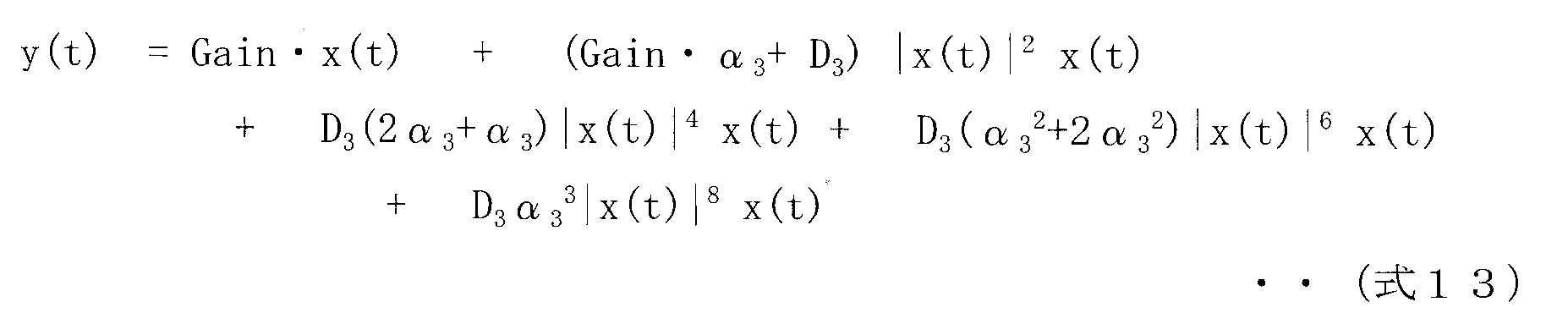
従って、(式10)において、プリディストータの次数を更に高次(5次、7次、・・・)についても考慮した場合には、3次のプリディストータの係数α3が、5次のプリディストータの係数α5や、7次のプリディストータの係数α7や、9次のプリディストータの係数α9などに影響を及ぼすため、α3の値に応じてα5、α7、α9などの最適値が変化してしまう。
なお、(式9)では、増幅器の非線形成分の次数を3次まで考慮したが、更に5次、7次、・・・などの高次を考慮した場合には、更に高次のプリディストータの係数に影響を及ぼすことになる。
次に、直交多項式を用いる本例の構成について詳しく説明する。
上述した問題を解決するために、本実施例では、非線形特性の逆特性の生成多項式として、直交多項式を導入して用いる。
本例では、直交多項式を用いて、複数あるプリディストータの生成多項式を直交させ、これにより、互いの係数が影響を及ぼさないように独立させて、収束時間を短くする。以下で、その一例を示す。

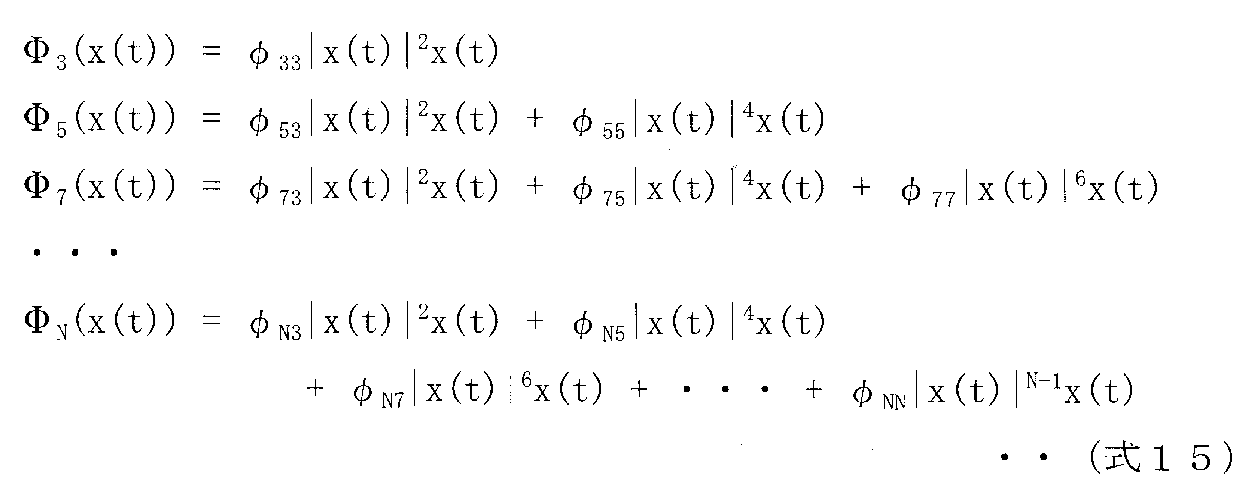
ここで、前記した時間(0~T)の時間Tとしては、1回の更新に用いられるデータの時間の長さであり、一般的に長い方が誤差が小さくなるため理想的には無限大がよいが、現実では、実用上で有効な程度で、任意の値が用いられてもよい。一例として、歪補償テーブル12の内容を毎回更新するときに、毎回異なる信号を直交させることとなることから、毎回直交させるために十分な入力信号の振幅分布が得られるような長さ(以上)の時間を用いることができ、例えば、原信号と同じ位の確率密度が得られるような長さ(以上)の時間を用いることができる。


以下では、E[・]の関数で表す。また、説明を簡易化するために、(式18)に示されるΦ3の場合と、(式19)に示されるΦ5の場合との二つの場合を示す。
Φ3とΦ5とが直交するためには、(式16)の関係を満たす必要があり、(式20)、(式21)、(式22)のような方程式が立てられる。



まず、(式20)をφ33について解くと、(式23)が得られる。
次に、(式21)により、(式24)が得られる。


そして、(式26)を(式24)に代入すると、(式27)が得られる。
このようにして、直交多項式を生成することができる。


一例として、Φ3、Φ5、Φ7を直交させる場合には、(式28)に示される連立方程式を満たす必要がある。この場合、6個の未知数φ33、φ53、φ55、φ73、φ75、φ77に対して、6本の方程式ができるため、これを解くことができる。同様に、Φ9以降についても拡張することができる。


この場合、プリディストーションの学習のための係数Aiは、Φi以外には影響を与えない、すなわち、他のプリディストーションの学習のための係数Aj(i≠j)とは独立して求めることができ、このため、収束時間が短くなる。具体的には、例えば、歪補償テーブル12の内容が初期状態(例えば、何の情報も無い状態)から収束するまでの更新回数が少なくなる。
上記した直交多項式を用いる構成では、収束時間を短くすることができるものの、直交多項式の効果を最大限には生かしておらず、更なる効率化を図ることが可能である。そこで、本例では、更なる効率化を図った構成例を示す。
初めに、図13には、図11に示されるプリディストータ付き増幅器の構成のように入力側のフィルタ(図1に示されるフィルタ16、18に相当するもの)及びフィードバック系のフィルタ(図1に示されるフィルタ8に相当するもの)が備えられていない場合として、例えば図12に示されるように波形比較法が用いられる場合について、E[Φm*・Φn]の一例を示してある。なお、送信信号としては、W-CDMA(Wideband-Code Division Multiple Access)の信号を用いている。
Aiは歪補償の係数(プリディストーションの学習のための係数)である。φijは、直交関数Φiを直交化させるためのパラメータ(直交化係数)である。
図13に示される表では、行(縦方向)に、入力側(送信側)の信号の成分Φ3 *、Φ5 *、Φ7 *を示してあり、図1に示されるような入力側のフィルタ16、18が備えられていない場合を示してある。
また、列(横方向)に、フィードバック側のエラー信号の成分Φ3、Φ5、Φ7を示してあり、図1に示されるようなフィードバック側のフィルタ8が備えられていない場合を示してある。
図13の例では、送信信号とフィードバック信号とでレベルや遅延時間などを理想的に調整してエラー信号を求めた場合には完全に直交することが確認された。
Aiは歪補償の係数(プリディストーションの学習のための係数)である。φijは、直交関数Φiを直交化させるためのパラメータ(直交化係数)である。
図14に示される表では、行(縦方向)に、入力側(送信側)の信号の成分Φ3 *、Φ5 *、Φ7 *を示してあり、図1に示されるような入力側のフィルタ16、18が備えられていない場合を示してある。
また、列(横方向)に、フィードバック側のエラー信号の成分Φ3、Φ5、Φ7を示してあり、図1に示されるようなフィードバック側のフィルタ8が備えられている場合を示してある。
図14の例では、E[Φm *・Φn](m≠n)と比較して、E[Φm *・Φn](m=n)の方が大きくなっているものの、直交性がかなり失われていることが確認された。
従って、収束時間が短く、且つ、ハードウエア規模を小さくする方法については、まだ改善する余地があり、更に効果的な方法の開発が期待される。
以下で、本例のプリディストータ付き増幅器における特徴的な構成について説明する。
概略的には、本例では、パラメータである直交化係数φijを算出する場合に、例えばBPFから構成されたフィルタで希望信号帯域を抑圧した信号を用いる。本例では、このフィルタはBPFであるとして説明する。
ここで、本例では、このフィルタの特性は、フィードバック系のフィルタ8や入力側の各フィルタ16、18の特性と同じであり、これら全てのフィルタが同じフィルタ特性を有している。
そして、BPFで希望信号帯域を抑圧した直交多項式を(式30)のように定義する。ここで、BPF[]は、希望信号帯域を抑圧した信号であることを表す。
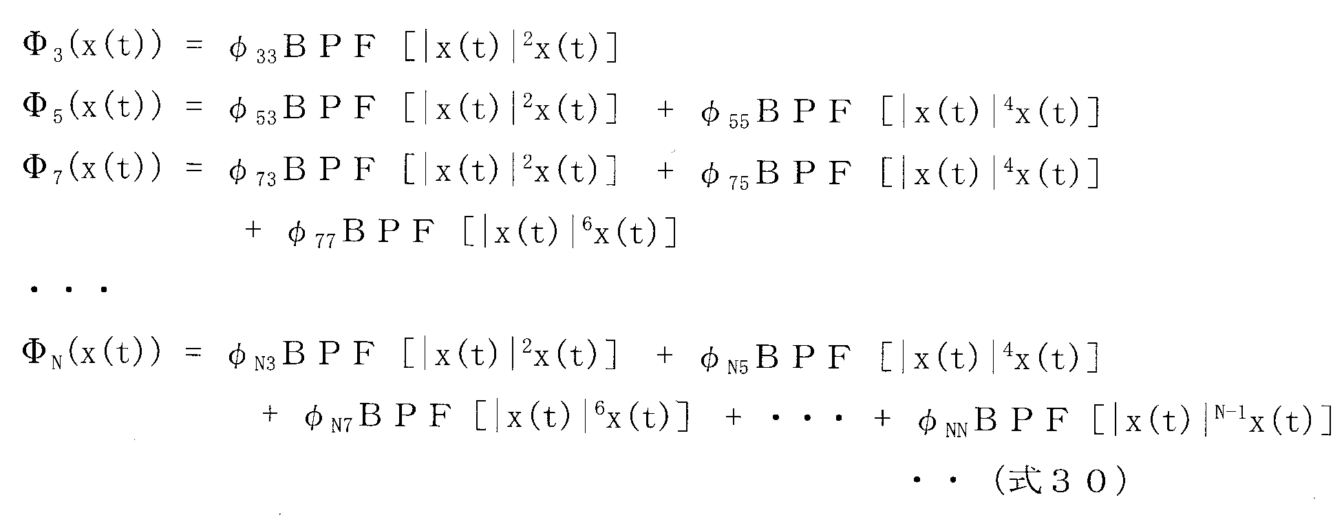
本例では、上記した(式15)ではなく、(式30)を用いて、パラメータである直交化係数φijを算出する。この算出の方法としては、上記した(式15)を用いた場合と同様な方法を用いることができる。
なお、上記した(式15)を用いた方法では(式31)が成り立つが、本例の(式30)を用いた方法では(式32)のようになる点が、異なる点であり、このため、それぞれ異なる直交化係数φijが求められる。
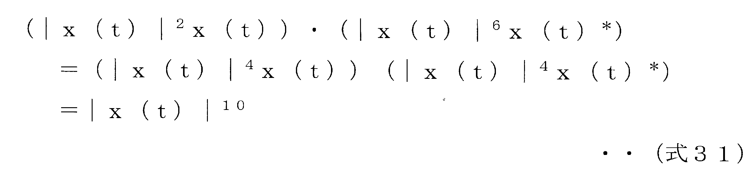

本例では、パラメータである直交化係数φijは、(式30)を用いて例えば計算機シミュレーションにより初めに求められたら、固定されて一定である。そして、直交化係数φijを用いて各直交関数Φiが求められる。
なお、直交関数Φiは、入力信号x(t)に応じて変動し、入力側についてもフィードバック側(歪成分)についても時間変動する。
また、列(横方向)に、フィードバック側のエラー信号の成分Φ3、Φ5、Φ7を示してあり、図1に示されるようなフィードバック側のフィルタ8が備えられている場合を示してある。
図5に示される本例の場合には、完全には直交しないものの、本例の(式30)を適用しない上記した図14の場合と比較すると、直交性が大きいことが確認された。
本例のように(式30)を用いて直交多項式の直交化係数φijを算出した場合には、例えば、(式15)を用いて直交多項式の直交化係数φijを算出した場合と比べて、更に、収束時間を短くして、効率化を図ることができる。
また、列(横方向)に、フィードバック側のエラー信号の成分Φ3、Φ5、Φ7を示してあり、図1に示されるようなフィードバック側のフィルタ8が備えられている場合を示してある。
図5に示される表の値と図6に示される表の値とは全く同じ値になっており、同じ直交の効果が得られることが確認された。
ここで、E[Φm *・Φn]は時間領域の畳み込みを行っているため、周波数領域では掛け算になっている。そして、一方(ここでは、フィードバック側)について帯域制限のフィルタで除去する、すなわち、0.0を乗算するため、結果は同じになることに着目した。
このような構成では、プリディストーションの学習のための係数を更新するたびに、T[sec](1回の更新に使用するデータ取得時間であり、任意の値)時間のデータを帯域制限することが不要となり、処理を簡単にすることができる。
本提案方式と比較方式とで収束時間を比較すると、比較方式では約500回であるのに対して、本提案方式では約100回で良好なACLRに収束することが確認された。本提案方式では、フィードバック信号に帯域制限のためのフィルタを用いる場合に、各係数の直交性が大きくなる、すなわち、独立して収束することが可能となるため、収束時間が短くなるという有効な効果が現れている。
一構成例として、入力側とフィードバック側の両方について、フィルタ(本例では、BPF)を用いて帯域制限を行う。
他の構成例として、LMSや摂動法などを用いてプリディストーションの学習のための係数Aiの学習の評価関数を求める際に、誤差信号e(t)にあたるフィードバック信号についてはフィルタ(本例では、BPF)で希望信号を除去し、これと相関を取るための入力側(送信側)の直交多項式の直交関数Φiについては帯域制限を行わないことによって、処理を簡単にすることができる。
本例では、メモリ効果プリディストータを用いる場合について説明する。
プリディストーション方式では、AM-AM変換やAM-PM変換の補償とともに、メモリ効果の補償が重要となる。一例として、特許文献2には、ベースバンド偶数次歪成分が電源回路のインピーダンスを介して電源電圧を変動させて入力信号を再変調し、帯域内奇数次成分を新しく発生させるメモリ効果を補償するプリディストータが示されている。
図8には、参考として、べき級数展開を用いたメモリ効果プリディストータの構成例を示してある。本例のメモリ効果プリディストータは、図1に示されるプリディストータ1に相当するものを原理的な構成例で示したものである。
また、本例のメモリ効果プリディストータは、全ての次数に共通な処理部として、加算器51を備えている。
2次の項に関する処理部では、2乗検出部41がプリディストータへの入力信号の2乗の値を検出(例えば、計算)し、遅延回路42が2乗検出部41からの出力(2乗値)をU[sec](好ましくは、1クロック時間)遅らせる。減算器43が、2乗検出部41の出力(2乗値)から、U[sec]前の2乗検出部41の出力(2乗値)を減算する。これにより、減算器43からの出力は、2乗値の差分となる。
そして、乗算器44が、2乗値の差分の値と入力信号とを乗算する。この乗算結果の出力信号は、キャリア信号が再変調された信号に相当し、3次成分となりキャリア周波数付近の周波数成分を有する。
複素乗算器45は、乗算器44からの出力信号にプリディストータの係数β2を乗算する。プリディストータの係数β2は複素数であり、制御部(図8では、図示せず)が歪を補償することができるように設定する。
そして、乗算器49が、4乗値の差分の値と入力信号とを乗算する。この乗算結果の出力信号は、キャリア信号が再変調された信号に相当し、5次成分となりキャリア周波数付近の周波数成分を有する。
複素乗算器50は、乗算器49からの出力信号にプリディストータの係数β4を乗算する。プリディストータの係数β4は複素数であり、制御部(図8では、図示せず)が歪を補償することができるように設定する。
そして、加算器51が、全ての偶数次の項の処理系(複素乗算器45、50、・・・)から出力される信号と入力信号を入力して加算(総和)し、当該加算結果をプリディストーション処理後の信号として(図1では、D/A変換器2へ)出力する。
なお、前記したU[sec]としては、例えば、(1クロック時間×1以上の整数)の値を用いることが可能である。
本例では、メモリ効果プリディストータの出力信号p(t)は、(式33)のように表される。
しかしながら、上記した第1実施例に係るメモリレスプリディストータの場合(AM-AM変換及びAM-PM変換を補償するプリディストータの係数の場合)と同様に、β2、β4、・・・を適応させる場合の収束時間が長くなるという問題があった。

上述した問題を解決するために、本実施例では、メモリ効果特性の逆特性の生成多項式として、直交多項式を導入して用いる。
本例では、直交多項式を用いて、複数あるプリディストータの生成多項式を直交させ、これにより、互いの係数が影響を及ぼさないように独立させて、収束時間を短くする。以下で、その一例を示す。

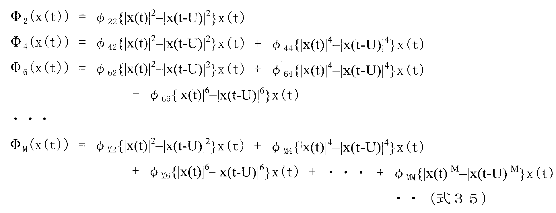
上記した第1実施例の場合と同様に、ある時間(0~T)の入力信号x(t)について、(式16)を満たすとき、(式35)に示されるそれぞれのΦ(Φ2~ΦM)が直交する。
説明を簡易化するために、Φ2の場合と、Φ4の場合との二つの場合を示す。
この場合、未知数φ22、φ42、φ44に対して、(式36)に示される3本の方程式ができるため、上記した第1実施例に係るAM-AM変換及びAM-PM変換を補償するプリディストータの場合と同様にして、解くことができる。

そして、上記した第1実施例で示した(式29)と同様に、B2、B4、B6、・・・、BMとβ2、β4、β6、・・・、βMとの関係を求めることができる。
このように、プリディストーションの学習のための係数Biは、Φi以外には影響を与えない、すなわち、他のプリディストーションの学習のための係数Bj(i≠j)とは独立して求めることができ、このため、収束時間が短くなる。
上記した直交多項式を用いる構成では、収束時間を短くすることができるものの、直交多項式の効果を最大限には生かしておらず、更なる効率化を図ることが可能である。そこで、本例では、更なる効率化を図った構成例を示す。
ここで、本例では、このフィルタの特性は、フィードバック系のフィルタ8や入力側の各フィルタ16、18の特性と同じであり、これら全てのフィルタが同じフィルタ特性を有している。
そして、BPFで希望信号帯域を抑圧した直交多項式を(式37)のように定義する。ここで、BPF[]は、希望信号帯域を抑圧した信号であることを表す。
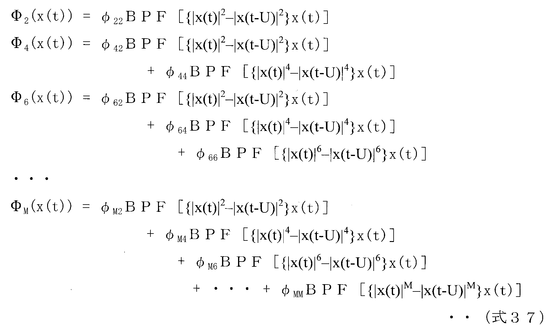
本例では、上記した(式35)ではなく、(式37)を用いて、パラメータである直交化係数φijを算出する。この算出の方法としては、上記した(式35)を用いた場合と同様な方法を用いることができる。
本例では、パラメータである直交化係数φijは、(式37)を用いて例えば計算機シミュレーションにより初めに求められたら、固定されて一定である。そして、直交化係数φijを用いて各直交関数Φiが求められる。
なお、直交関数Φiは、入力信号x(t)に応じて変動し、入力側についてもフィードバック側(歪成分)についても時間変動する。
本例のように(式37)を用いて直交多項式の直交化係数φijを算出した場合には、例えば、(式35)を用いて直交多項式の直交化係数φijを算出した場合と比べて、更に、収束時間を短くして、効率化を図ることができる。
このような構成では、プリディストーションの学習のための係数を更新するたびに、T[sec](1回の更新に使用するデータ取得時間であり、任意の値)時間のデータを帯域制限することが不要となり、処理を簡単にすることができる。
一構成例として、入力側とフィードバック側の両方について、フィルタ(本例では、BPF)を用いて帯域制限を行う。
他の構成例として、LMSや摂動法などを用いてプリディストーションの学習のための係数Biの学習の評価関数を求める際に、誤差信号e(t)にあたるフィードバック信号についてはフィルタ(本例では、BPF)で希望信号を除去し、これと相関を取るための入力側(送信側)の直交多項式の直交関数Φiについては帯域制限を行わないことによって、処理を簡単にすることができる。
本例では、メモリレスプリディストータ及びメモリ効果プリディストータの両方を並列に用いる場合について説明する。
図9には、本発明の一実施例に係るプリディストータの構成例を示してある。
本例のプリディストータでは、AM-AM変換とAM-PM変換を補償するとともに、メモリ効果を補償する。
ここで、メモリレスPD61としては、図4に示されるような原理構成のものなどを用いることができ、また、メモリ効果PD62としては、図8に示されるような原理構成のものなどを用いることができる。
なお、本例では、メモリレスPD61やメモリ効果PD62はそれぞれ図1に示されるプリディストータ1に相当しており、図4に示されるメモリレスPDの加算器27と図8に示されるメモリ効果PDの加算器51が共通化されて図9に示される加算器64になっていると捉えることが可能である。
本例では、直交多項式を用いて、複数あるプリディストータの生成多項式を直交させ、これにより、互いの係数が影響を及ぼさないように独立させて、収束時間を短くする。
本例では、それぞれのプリディストータ61、62からの出力信号が加算器63により加算されて、非線形特性の逆特性を与える当該加算結果の信号p(t)が加算器64により入力信号と加算される。
p(t)は、上記した(式7)及び(式33)により、(式38)のように表される。
本例では、(式38)を(式39)、(式40)のように表現する。

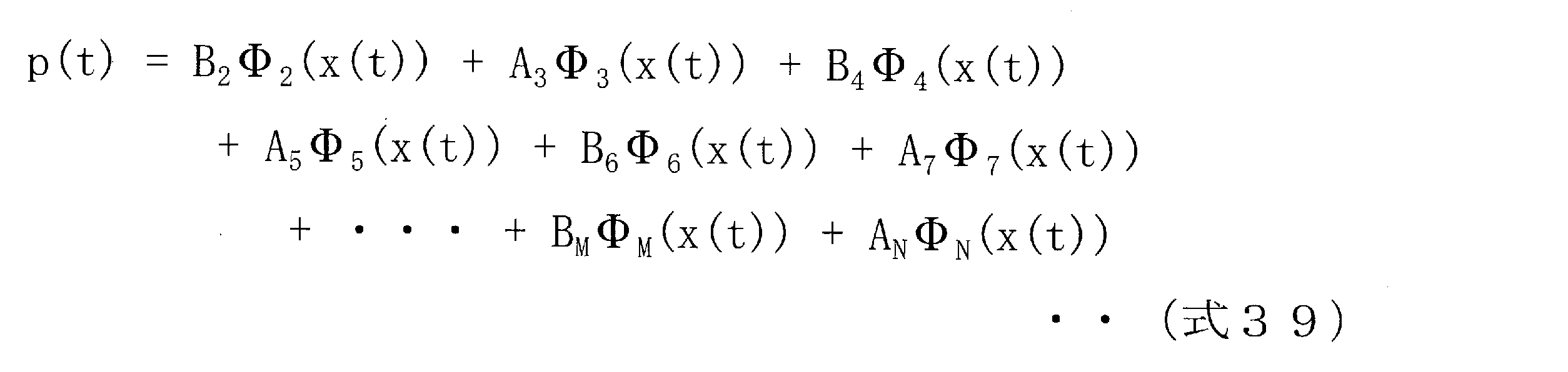
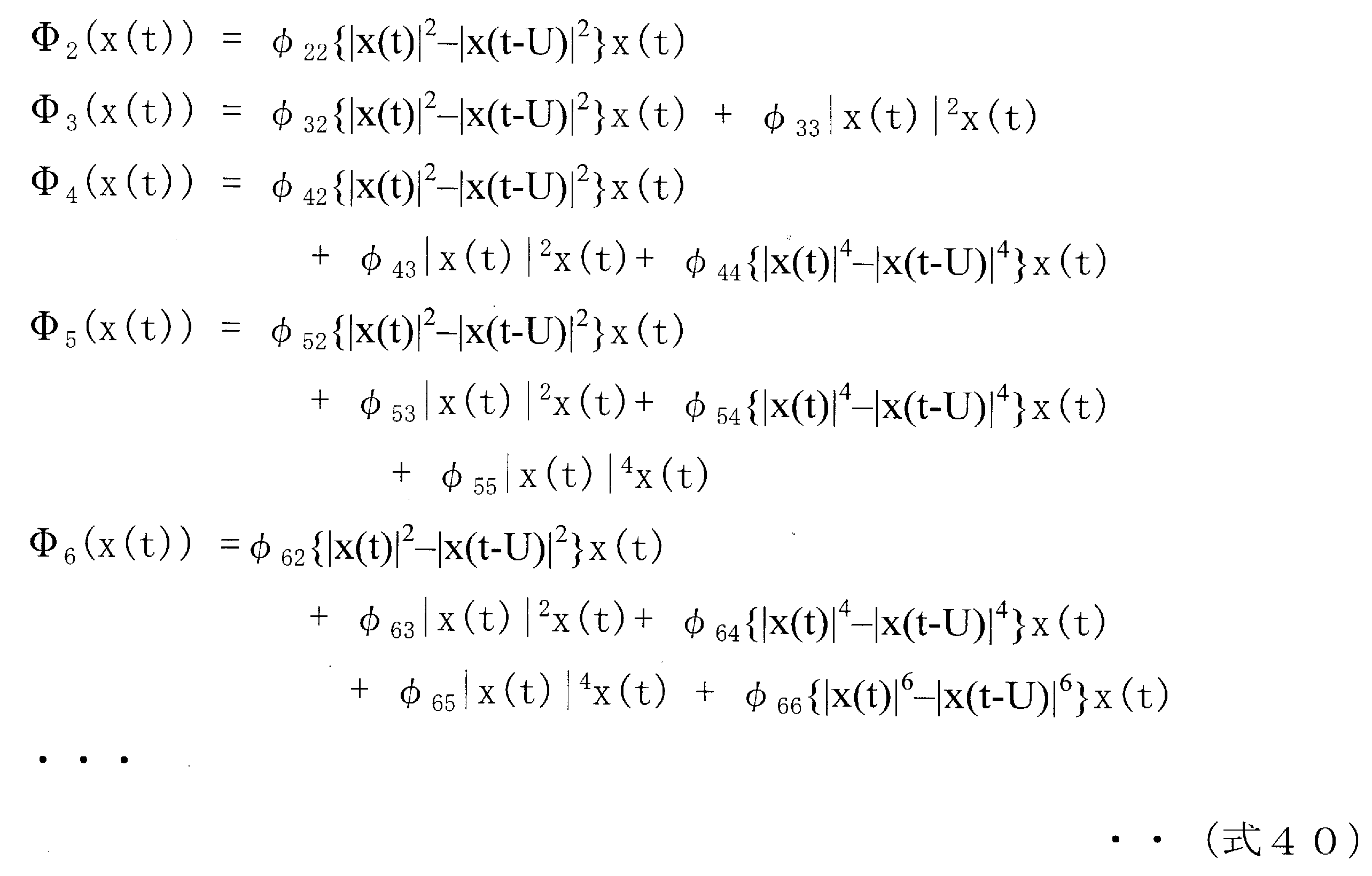
この場合、B2、A3、B4、A5、B6、A7、・・・は、互いに独立となるため、収束時間が短くなる。
本例では、メモリレスPD61とメモリ効果PD62との相互作用も(式40)に入っており、全てのプリディストーションの学習のための係数Ai、Bjを直交化させることができる。
上記した直交多項式を用いる構成では、収束時間を短くすることができるものの、直交多項式の効果を最大限には生かしておらず、更なる効率化を図ることが可能である。そこで、本例では、更なる効率化を図った構成例を示す。
ここで、本例では、このフィルタの特性は、フィードバック系のフィルタ8や入力側の各フィルタ16、18の特性と同じであり、これら全てのフィルタが同じフィルタ特性を有している。
そして、BPFで希望信号帯域を抑圧した直交多項式を(式42)のように定義する。ここで、BPF[]は、希望信号帯域を抑圧した信号であることを表す。
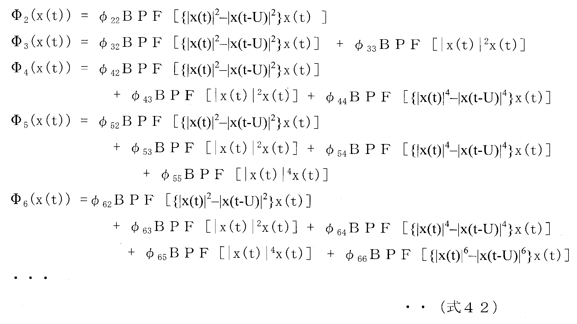
本例では、上記した(式40)ではなく、(式42)を用いて、パラメータである直交化係数φijを算出する。この算出の方法としては、上記した(式40)を用いた場合と同様な方法を用いることができる。
本例では、パラメータである直交化係数φijは、(式42)を用いて例えば計算機シミュレーションにより初めに求められたら、固定されて一定である。そして、直交化係数φijを用いて各直交関数Φiが求められる。
なお、直交関数Φiは、入力信号x(t)に応じて変動し、入力側についてもフィードバック側(歪成分)についても時間変動する。
本例のように(式42)を用いて直交多項式の直交化係数φijを算出した場合には、例えば、(式40)を用いて直交多項式の直交化係数φijを算出した場合と比べて、更に、収束時間を短くして、効率化を図ることができる。
このような構成では、プリディストーションの学習のための係数を更新するたびに、T[sec](1回の更新に使用するデータ取得時間であり、任意の値)時間のデータを帯域制限することが不要となり、処理を簡単にすることができる。
一構成例として、入力側とフィードバック側の両方について、フィルタ(本例では、BPF)を用いて帯域制限を行う。
他の構成例として、LMSや摂動法などを用いてプリディストーションの学習のための係数Ai、Biの学習の評価関数を求める際に、誤差信号e(t)にあたるフィードバック信号についてはフィルタ(本例では、BPF)で希望信号を除去し、これと相関を取るための入力側(送信側)の直交多項式の直交関数Φiについては帯域制限を行わないことによって、処理を簡単にすることができる。
図10には、本発明の一実施例に係るプリディストータ付き増幅器の他の構成例を示してある。
本例のプリディストータ付き増幅器の構成や動作は、例えば、図1に示されるプリディストータ付き増幅器の構成や動作と比べて、Φ3取得部15、フィルタ16、Φ5取得部17、フィルタ18が備えられていない点で異なっている。
この場合、制御部14は、フィードバックされた歪成分(歪成分全体)の信号に基づいて、それが小さくなるように制御を行う。
このため、上記した第1実施例~第3実施例では、図1に示されるプリディストータ付き増幅器を用いた場合を示したが、その代わりに、図10に示されるプリディストータ付き増幅器を用いることも可能であり、つまり、図10に示されるプリディストータ付き増幅器において、直交化係数φijの算出に、フィルタ(本例では、BPF)で希望信号帯域を抑圧した信号を用いる構成とすることも可能である。
なお、図1や図10に示される本例のプリディストータ付き増幅器(歪補償増幅装置の一例)では、振幅検出部11の機能によりレベル検出手段が構成されており、歪補償テーブル(LUT)12の機能により対応記憶手段が構成されており、プリディストーション実行部13の機能によりプリディストーション実行手段が構成されており、フィルタ8の機能によりフィルタ手段が構成されており、制御部(学習)14の機能により対応取得手段が構成されており、Φ3取得部15やΦ5取得部17の機能により入力信号関数値取得手段が構成されている。
[以上、以上に示した実施例における機能手段や用語の説明]
以上に示した実施例から把握される歪補償増幅装置の構成例を示す。
第1構成例は、増幅器のもつ非線形特性によって発生する歪を補償するために前記非線形特性の逆特性をもつ信号を生成して前記増幅器に出力するプリディストータを有する歪補償増幅装置において、
前記プリディストータに入力される信号のレベルを検出するレベル検出手段と、
前記プリディストータに入力される信号のレベルとプリディストーションを実行するための歪補償係数との対応を記憶する対応記憶手段と、
前記プリディストータに入力される信号に対して前記プリディストーションを実行するための歪補償係数に基づいて前記増幅器のもつ非線形特性の逆特性を与え、前記増幅器に出力するプリディストーション実行手段と、
前記増幅器出力のフィードバック信号から希望波周波数成分を除去して歪信号成分を出力するフィルタ手段と、
前記フィルタ手段により取得された前記歪信号成分が小さくなるように前記プリディストータに入力される信号に対して増幅器のもつ非線形特性の逆特性を与える関数を構成するプリディストーションの学習のための係数を更新し、更新した前記プリディストーションの学習のための係数に基づいて前記プリディストータに入力される信号のレベルと前記プリディストーションを実行するための歪補償係数との対応を取得して前記対応記憶手段に出力する対応取得手段と、を備え、
前記増幅器のもつ非線形特性の逆特性を与える関数には直交多項式を用い、
前記直交多項式を構成する各直交関数は、1個以上の入力信号の関数と、前記入力信号の関数にそれぞれ対応するパラメータとの積の総和であり、
前記1個以上の入力信号の関数にそれぞれ対応するパラメータの値は、前記入力信号の関数に前記フィルタ手段と同一のフィルタ特性を有するフィルタをかけて得られる関数を前記各直交関数を構成する前記入力信号の関数と置換した場合に前記各直交関数が互いに直交するように設定される、
ことを特徴とする歪補償増幅装置である。
前記プリディストータに入力される信号に基づいて、前記各直交関数を構成する前記各入力信号の関数により得られる信号をそれぞれ取得する関数信号取得手段を備え、
前記対応取得手段は、前記関数信号取得手段により取得した信号と前記フィルタ手段により取得した歪信号成分とをそれぞれ複素乗算することにより前記歪信号成分から前記1個以上の直交関数のそれぞれに対応した信号成分を抽出し、前記抽出した信号成分毎にそれが小さくなるように、前記プリディストーションの学習のための係数を更新する、
ことを特徴とする歪補償増幅装置である。
前記プリディストータに入力される信号に基づいて、前記各直交関数を構成する前記各入力信号の関数により得られる信号をそれぞれ取得する関数信号取得手段と、
前記関数信号取得手段により取得した信号に対して、前記フィルタ手段と同一のフィルタ特性を有するフィルタをかけた信号をそれぞれ取得する関数信号フィルタ手段と、を備え、
前記対応取得手段は、前記関数信号フィルタ手段により取得した信号と前記フィルタ手段により取得した歪信号成分とをそれぞれ複素乗算することにより前記歪信号成分から前記1個以上の直交関数のそれぞれに対応した信号成分を抽出し、前記抽出した信号成分毎にそれが小さくなるように、前記プリディストーションの学習のための係数を更新する、
ことを特徴とする歪補償増幅装置である。
なお、第3構成例は、第2構成例における入力信号側(Φ)にフィルタを設けた構成例である。
前記対応取得手段は、前記フィルタ手段により取得した前記歪信号成分のみを用いて、当該歪信号成分の全体が小さくなるように、前記プリディストーションの学習のための係数を更新する、
ことを特徴とする歪補償増幅装置である。
第1~第4構成例では、振幅検出部11の機能によりレベル検出手段が構成されており、歪補償テーブル(LUT)12の機能により対応記憶手段が構成されており、プリディストーション実行部13の機能によりプリディストーション実行手段が構成されており、フィルタ8の機能によりフィルタ手段が構成されており、制御部(学習)14の機能により対応取得手段が構成されており、Φ3取得部15やΦ5取得部17の機能により関数信号取得手段(前記した入力信号関数値取得手段に対応する手段)が構成されており、フィルタ16やフィルタ18の機能により関数信号フィルタ手段が構成されている。
[以上、以上に示した実施例から把握される歪補償増幅装置の構成例]
また、本発明の適用分野としては、必ずしも以上に示したものに限られず、本発明は、種々な分野に適用することが可能なものである。
また、本発明に係るシステムや装置などにおいて行われる各種の処理としては、例えばプロセッサやメモリ等を備えたハードウエア資源においてプロセッサがROM(Read Only Memory)に格納された制御プログラムを実行することにより制御される構成が用いられてもよく、また、例えば当該処理を実行するための各機能手段が独立したハードウエア回路として構成されてもよい。
また、本発明は上記の制御プログラムを格納したフロッピー(登録商標)ディスクやCD(Compact Disc)-ROM等のコンピュータにより読み取り可能な記録媒体や当該プログラム(自体)として把握することもでき、当該制御プログラムを当該記録媒体からコンピュータに入力してプロセッサに実行させることにより、本発明に係る処理を遂行させることができる。
Claims (4)
- 増幅器のもつ非線形特性によって発生する歪を補償するために前記非線形特性の逆特性をもつ信号を生成して前記増幅器に出力するプリディストータを有する歪補償増幅装置において、
前記プリディストータに入力される信号のレベルを検出するレベル検出手段と、
前記プリディストータに入力される信号のレベルとプリディストーションを実行するための歪補償係数との対応を記憶する対応記憶手段と、
前記プリディストータに入力される信号に対して前記プリディストーションを実行するための歪補償係数に基づいて前記増幅器のもつ非線形特性の逆特性を与え、前記増幅器に出力するプリディストーション実行手段と、
前記増幅器出力のフィードバック信号から希望波周波数成分を除去して歪信号成分を出力するフィルタ手段と、
前記フィルタ手段により取得された前記歪信号成分が小さくなるように前記プリディストータに入力される信号に対して増幅器のもつ非線形特性の逆特性を与える関数を構成するプリディストーションの学習のための係数を更新し、更新した前記プリディストーションの学習のための係数に基づいて前記プリディストータに入力される信号のレベルと前記プリディストーションを実行するための歪補償係数との対応を取得して前記対応記憶手段に出力する対応取得手段と、を備え、
前記増幅器のもつ非線形特性の逆特性を与える関数には直交多項式を用い、
前記直交多項式を構成する各直交関数は、1個以上の入力信号の関数と、前記入力信号の関数にそれぞれ対応するパラメータとの積の総和であり、
前記1個以上の入力信号の関数にそれぞれ対応するパラメータの値は、前記入力信号の関数に前記フィルタ手段と同一のフィルタ特性を有するフィルタをかけて得られる関数を前記各直交関数を構成する前記入力信号の関数と置換した場合に前記各直交関数が互いに直交するように設定される、
ことを特徴とする歪補償増幅装置。 - 請求項1に記載の歪補償増幅装置において、
前記プリディストータに入力される信号に基づいて、前記各直交関数を構成する前記各入力信号の関数により得られる信号をそれぞれ取得する関数信号取得手段を備え、
前記対応取得手段は、前記関数信号取得手段により取得した信号と前記フィルタ手段により取得した歪信号成分とをそれぞれ複素乗算することにより前記歪信号成分から前記1個以上の直交関数のそれぞれに対応した信号成分を抽出し、前記抽出した信号成分毎にそれが小さくなるように、前記プリディストーションの学習のための係数を更新する、
ことを特徴とする歪補償増幅装置。 - 請求項1に記載の歪補償増幅装置において、
前記プリディストータに入力される信号に基づいて、前記各直交関数を構成する前記各入力信号の関数により得られる信号をそれぞれ取得する関数信号取得手段と、
前記関数信号取得手段により取得した信号に対して、前記フィルタ手段と同一のフィルタ特性を有するフィルタをかけた信号をそれぞれ取得する関数信号フィルタ手段と、を備え、
前記対応取得手段は、前記関数信号フィルタ手段により取得した信号と前記フィルタ手段により取得した歪信号成分とをそれぞれ複素乗算することにより前記歪信号成分から前記1個以上の直交関数のそれぞれに対応した信号成分を抽出し、前記抽出した信号成分毎にそれが小さくなるように、前記プリディストーションの学習のための係数を更新する、
ことを特徴とする歪補償増幅装置。 - 請求項1に記載の歪補償増幅装置において、
前記対応取得手段は、前記フィルタ手段により取得した前記歪信号成分のみを用いて、当該歪信号成分の全体が小さくなるように、前記プリディストーションの学習のための係数を更新する、
ことを特徴とする歪補償増幅装置。
Priority Applications (2)
| Application Number | Priority Date | Filing Date | Title |
|---|---|---|---|
| US13/062,039 US8334723B2 (en) | 2008-09-09 | 2009-08-24 | Distortion compensation amplification device |
| CN200980129298.3A CN102106079B (zh) | 2008-09-09 | 2009-08-24 | 预失真器 |
Applications Claiming Priority (2)
| Application Number | Priority Date | Filing Date | Title |
|---|---|---|---|
| JP2008231317A JP5205182B2 (ja) | 2008-09-09 | 2008-09-09 | 歪補償増幅装置 |
| JP2008-231317 | 2008-09-09 |
Publications (1)
| Publication Number | Publication Date |
|---|---|
| WO2010029690A1 true WO2010029690A1 (ja) | 2010-03-18 |
Family
ID=42004956
Family Applications (1)
| Application Number | Title | Priority Date | Filing Date |
|---|---|---|---|
| PCT/JP2009/004050 Ceased WO2010029690A1 (ja) | 2008-09-09 | 2009-08-24 | 歪補償増幅装置 |
Country Status (4)
| Country | Link |
|---|---|
| US (1) | US8334723B2 (ja) |
| JP (1) | JP5205182B2 (ja) |
| CN (1) | CN102106079B (ja) |
| WO (1) | WO2010029690A1 (ja) |
Cited By (1)
| Publication number | Priority date | Publication date | Assignee | Title |
|---|---|---|---|---|
| JP2009200694A (ja) * | 2008-02-20 | 2009-09-03 | Japan Radio Co Ltd | 歪補償回路及びプリディストーション型歪補償増幅器 |
Families Citing this family (35)
| Publication number | Priority date | Publication date | Assignee | Title |
|---|---|---|---|---|
| US8792581B2 (en) * | 2010-02-18 | 2014-07-29 | Telefonaktiebolaget Lm Ericsson (Publ) | RF clock generator with spurious tone cancellation |
| JP5499878B2 (ja) * | 2010-04-23 | 2014-05-21 | 富士通株式会社 | 歪補償装置、無線通信装置及び歪補償方法 |
| US10387592B1 (en) | 2010-05-26 | 2019-08-20 | Keysight Technologies, Inc. | Method and system for characterizing, modeling and simulating non-linear components having long term memory effects |
| JP6037493B2 (ja) | 2011-10-13 | 2016-12-07 | 株式会社日立国際電気 | 歪み補償回路および歪み補償回路と高周波電力増幅器を用いた送信装置 |
| US8914271B2 (en) * | 2011-11-30 | 2014-12-16 | Keysight Technologies, Inc. | Method for predistorting signals for non-linear components in the presence of long term memory effects |
| CN103581082B (zh) * | 2012-07-31 | 2016-10-05 | 富士通株式会社 | 基带预失真的系数更新装置及方法、预失真设备及发射机 |
| WO2014021895A1 (en) * | 2012-08-02 | 2014-02-06 | Texas State University - San Marcos | Suppression of interference in power and communication signals |
| JP6098336B2 (ja) | 2012-09-25 | 2017-03-22 | 住友電気工業株式会社 | 歪補償装置および無線通信装置 |
| US9319002B2 (en) * | 2012-09-25 | 2016-04-19 | Hitachi Kokusai Electric Inc. | Distortion compensation circuit and transmission device using distortion compensation circuit and high-frequency power amplifier |
| JP2014116691A (ja) | 2012-12-06 | 2014-06-26 | Samsung Electronics Co Ltd | 高周波増幅装置及び歪補償方法 |
| WO2014088367A1 (en) * | 2012-12-06 | 2014-06-12 | Samsung Electronics Co., Ltd. | High frequency amplifier and method of compensating for distortion |
| JP5958324B2 (ja) | 2012-12-19 | 2016-07-27 | 富士通株式会社 | 歪補償装置および電力増幅装置の歪補償方法 |
| JP6296709B2 (ja) * | 2013-06-14 | 2018-03-20 | 株式会社東芝 | 歪補償装置 |
| TWI560998B (en) * | 2013-07-11 | 2016-12-01 | Realtek Semiconductor Corp | Pre-distortion method, pre-distortion apparatus and machine readable medium |
| JP2015142325A (ja) * | 2014-01-30 | 2015-08-03 | 富士通株式会社 | 歪補償装置および歪補償方法 |
| JP5918820B2 (ja) * | 2014-09-01 | 2016-05-18 | アンリツ株式会社 | 測定装置及び測定方法 |
| US9590567B2 (en) | 2015-07-02 | 2017-03-07 | Xilinx, Inc. | Moving mean and magnitude dual path digital predistortion |
| US9590668B1 (en) * | 2015-11-30 | 2017-03-07 | NanoSemi Technologies | Digital compensator |
| US10812166B2 (en) | 2016-10-07 | 2020-10-20 | Nanosemi, Inc. | Beam steering digital predistortion |
| KR20190121825A (ko) | 2017-02-25 | 2019-10-28 | 나노세미, 인크. | 멀티밴드 디지털 전치왜곡기 |
| US10141961B1 (en) | 2017-05-18 | 2018-11-27 | Nanosemi, Inc. | Passive intermodulation cancellation |
| US11115067B2 (en) | 2017-06-09 | 2021-09-07 | Nanosemi, Inc. | Multi-band linearization system |
| US10581470B2 (en) | 2017-06-09 | 2020-03-03 | Nanosemi, Inc. | Linearization system |
| US10931318B2 (en) * | 2017-06-09 | 2021-02-23 | Nanosemi, Inc. | Subsampled linearization system |
| US11323188B2 (en) | 2017-07-12 | 2022-05-03 | Nanosemi, Inc. | Monitoring systems and methods for radios implemented with digital predistortion |
| US11303251B2 (en) | 2017-10-02 | 2022-04-12 | Nanosemi, Inc. | Digital predistortion adjustment based on determination of load condition characteristics |
| US10644657B1 (en) | 2018-05-11 | 2020-05-05 | Nanosemi, Inc. | Multi-band digital compensator for a non-linear system |
| JP2021523629A (ja) | 2018-05-11 | 2021-09-02 | ナノセミ, インク.Nanosemi, Inc. | 非線形システム用デジタル補償器 |
| CN112640299B (zh) | 2018-05-25 | 2024-11-12 | 纳诺塞米有限公司 | 用于数字预失真的方法、用于执行数字预失真的线性化系统和非暂时性机器可读介质 |
| US11863210B2 (en) | 2018-05-25 | 2024-01-02 | Nanosemi, Inc. | Linearization with level tracking |
| US10931238B2 (en) | 2018-05-25 | 2021-02-23 | Nanosemi, Inc. | Linearization with envelope tracking or average power tracking |
| JP7367557B2 (ja) * | 2020-02-21 | 2023-10-24 | 富士通オプティカルコンポーネンツ株式会社 | 光通信装置及び補正方法 |
| US10992326B1 (en) | 2020-05-19 | 2021-04-27 | Nanosemi, Inc. | Buffer management for adaptive digital predistortion |
| CN116406496A (zh) | 2020-10-30 | 2023-07-07 | 富士通株式会社 | 测量非线性器件的非线性相关参数的方法、装置和系统 |
| CN113676259B (zh) * | 2021-07-30 | 2022-07-26 | 华南师范大学 | 基于Legendre多项式的LED非线性补偿方法、系统、设备及介质 |
Citations (4)
| Publication number | Priority date | Publication date | Assignee | Title |
|---|---|---|---|---|
| JPH11154880A (ja) * | 1997-09-05 | 1999-06-08 | Fujitsu Ltd | 信号補正方法及び装置、歪補償装置、歪補償データ作成装置及び送信機 |
| JP2006093947A (ja) * | 2004-09-22 | 2006-04-06 | Japan Radio Co Ltd | プリディストーション型歪補償増幅回路 |
| JP2007129492A (ja) * | 2005-11-02 | 2007-05-24 | Japan Radio Co Ltd | プリディストーション型歪補償増幅器 |
| JP2007208315A (ja) * | 2006-01-30 | 2007-08-16 | Hiroshi Ogawa | 歪補償回路 |
Family Cites Families (9)
| Publication number | Priority date | Publication date | Assignee | Title |
|---|---|---|---|---|
| JP3171157B2 (ja) * | 1997-12-10 | 2001-05-28 | 松下電器産業株式会社 | 非線形歪補償装置 |
| US6288610B1 (en) | 1998-03-19 | 2001-09-11 | Fujitsu Limited | Method and apparatus for correcting signals, apparatus for compensating for distortion, apparatus for preparing distortion compensating data, and transmitter |
| JP2004112151A (ja) | 2002-09-17 | 2004-04-08 | Hitachi Kokusai Electric Inc | 歪み補償方法及び送信機 |
| JP4394409B2 (ja) | 2003-09-25 | 2010-01-06 | 株式会社日立国際電気 | プリディストーション方式歪補償機能付き増幅器 |
| JP2005341117A (ja) * | 2004-05-26 | 2005-12-08 | Nippon Telegr & Teleph Corp <Ntt> | 非線形歪補償装置 |
| JP4537187B2 (ja) * | 2004-12-06 | 2010-09-01 | 株式会社日立国際電気 | 増幅装置 |
| JP4825495B2 (ja) * | 2005-11-10 | 2011-11-30 | 株式会社日立国際電気 | 歪制御機能付き増幅装置 |
| CN104202279A (zh) * | 2006-12-26 | 2014-12-10 | 大力系统有限公司 | 用于多信道宽带通信系统中的基带预失真线性化的方法和系统 |
| JP2009111958A (ja) * | 2007-11-01 | 2009-05-21 | Hitachi Kokusai Electric Inc | プリディストータ |
-
2008
- 2008-09-09 JP JP2008231317A patent/JP5205182B2/ja active Active
-
2009
- 2009-08-24 WO PCT/JP2009/004050 patent/WO2010029690A1/ja not_active Ceased
- 2009-08-24 US US13/062,039 patent/US8334723B2/en not_active Expired - Fee Related
- 2009-08-24 CN CN200980129298.3A patent/CN102106079B/zh not_active Expired - Fee Related
Patent Citations (4)
| Publication number | Priority date | Publication date | Assignee | Title |
|---|---|---|---|---|
| JPH11154880A (ja) * | 1997-09-05 | 1999-06-08 | Fujitsu Ltd | 信号補正方法及び装置、歪補償装置、歪補償データ作成装置及び送信機 |
| JP2006093947A (ja) * | 2004-09-22 | 2006-04-06 | Japan Radio Co Ltd | プリディストーション型歪補償増幅回路 |
| JP2007129492A (ja) * | 2005-11-02 | 2007-05-24 | Japan Radio Co Ltd | プリディストーション型歪補償増幅器 |
| JP2007208315A (ja) * | 2006-01-30 | 2007-08-16 | Hiroshi Ogawa | 歪補償回路 |
Cited By (1)
| Publication number | Priority date | Publication date | Assignee | Title |
|---|---|---|---|---|
| JP2009200694A (ja) * | 2008-02-20 | 2009-09-03 | Japan Radio Co Ltd | 歪補償回路及びプリディストーション型歪補償増幅器 |
Also Published As
| Publication number | Publication date |
|---|---|
| JP5205182B2 (ja) | 2013-06-05 |
| US8334723B2 (en) | 2012-12-18 |
| JP2010068142A (ja) | 2010-03-25 |
| US20110163806A1 (en) | 2011-07-07 |
| CN102106079B (zh) | 2014-01-29 |
| CN102106079A (zh) | 2011-06-22 |
Similar Documents
| Publication | Publication Date | Title |
|---|---|---|
| JP5205182B2 (ja) | 歪補償増幅装置 | |
| JP2009111958A (ja) | プリディストータ | |
| JP5402817B2 (ja) | 電力増幅器のメモリ効果キャンセラ、無線送信機 | |
| JP5236661B2 (ja) | 多チャンネル広帯域通信システムにおけるベースバンドプリディストーション線形化の方法及びシステム | |
| JP5120178B2 (ja) | 非線形システム逆特性同定装置及びその方法、電力増幅装置及び電力増幅器のプリディストータ | |
| KR100837743B1 (ko) | Rf 전력 증폭기 내에서 메모리 효과들을 정정하는 디지털 전치 왜곡 시스템 및 방법 | |
| JP4394409B2 (ja) | プリディストーション方式歪補償機能付き増幅器 | |
| JP4417174B2 (ja) | プリディストータ | |
| US8787494B2 (en) | Modeling digital predistorter | |
| JP4835241B2 (ja) | ディジタルプリディストーション送信機 | |
| JP5516269B2 (ja) | 増幅装置およびプリディストーション制御方法 | |
| JP5664116B2 (ja) | 電力増幅装置及びその歪補償係数更新方法及び送信装置 | |
| Zhu et al. | An adaptive Volterra predistorter for the linearization of RF high power amplifiers | |
| US6956433B2 (en) | Polynomial predistorter using complex vector multiplication | |
| JP2005217690A (ja) | プリディストータ | |
| WO2013153485A1 (en) | Digital predistorter (dpd) structure based on dynamic deviation reduction (ddr)-based volterra series | |
| CN107786174B (zh) | 用于预失真的电路和方法 | |
| JP4918572B2 (ja) | プリディストーション方式歪補償機能付き増幅器 | |
| WO2011112129A1 (en) | A decomposition transmitting system and method for improving efficiency and linearity | |
| CN112859611A (zh) | 一种自适应预失真系统及方法 | |
| JP2014116691A (ja) | 高周波増幅装置及び歪補償方法 | |
| Harmon et al. | Iterative approach to the indirect learning architecture for baseband digital predistortion | |
| CN114584081B (zh) | 数字预畸变处理方法、wifi宽带系统和计算机存储介质 | |
| KR20240152218A (ko) | 복잡도가 낮은 직접-lut(direct-to-lut) 디지털 전치 왜곡 방법 | |
| JP2016167763A (ja) | 歪補償装置及び歪補償方法 |
Legal Events
| Date | Code | Title | Description |
|---|---|---|---|
| WWE | Wipo information: entry into national phase |
Ref document number: 200980129298.3 Country of ref document: CN |
|
| 121 | Ep: the epo has been informed by wipo that ep was designated in this application |
Ref document number: 09812839 Country of ref document: EP Kind code of ref document: A1 |
|
| WWE | Wipo information: entry into national phase |
Ref document number: 13062039 Country of ref document: US |
|
| NENP | Non-entry into the national phase |
Ref country code: DE |
|
| 122 | Ep: pct application non-entry in european phase |
Ref document number: 09812839 Country of ref document: EP Kind code of ref document: A1 |