WO2010023741A1 - 圧電振動片の製造方法、圧電振動子、発振器、電子機器及び電波時計 - Google Patents
圧電振動片の製造方法、圧電振動子、発振器、電子機器及び電波時計 Download PDFInfo
- Publication number
- WO2010023741A1 WO2010023741A1 PCT/JP2008/065369 JP2008065369W WO2010023741A1 WO 2010023741 A1 WO2010023741 A1 WO 2010023741A1 JP 2008065369 W JP2008065369 W JP 2008065369W WO 2010023741 A1 WO2010023741 A1 WO 2010023741A1
- Authority
- WO
- WIPO (PCT)
- Prior art keywords
- protective film
- wafer
- piezoelectric
- groove
- piezoelectric vibrating
- Prior art date
- Legal status (The legal status is an assumption and is not a legal conclusion. Google has not performed a legal analysis and makes no representation as to the accuracy of the status listed.)
- Ceased
Links
Images













Classifications
-
- H—ELECTRICITY
- H03—ELECTRONIC CIRCUITRY
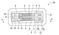
- H03H—IMPEDANCE NETWORKS, e.g. RESONANT CIRCUITS; RESONATORS
- H03H3/00—Apparatus or processes specially adapted for the manufacture of impedance networks, resonating circuits, resonators
- H03H3/007—Apparatus or processes specially adapted for the manufacture of impedance networks, resonating circuits, resonators for the manufacture of electromechanical resonators or networks
- H03H3/02—Apparatus or processes specially adapted for the manufacture of impedance networks, resonating circuits, resonators for the manufacture of electromechanical resonators or networks for the manufacture of piezoelectric or electrostrictive resonators or networks
- H03H3/04—Apparatus or processes specially adapted for the manufacture of impedance networks, resonating circuits, resonators for the manufacture of electromechanical resonators or networks for the manufacture of piezoelectric or electrostrictive resonators or networks for obtaining desired frequency or temperature coefficient
-
- H—ELECTRICITY
- H03—ELECTRONIC CIRCUITRY
- H03H—IMPEDANCE NETWORKS, e.g. RESONANT CIRCUITS; RESONATORS
- H03H9/00—Networks comprising electromechanical or electro-acoustic elements; Electromechanical resonators
- H03H9/02—Details
- H03H9/05—Holders or supports
- H03H9/10—Mounting in enclosures
- H03H9/1007—Mounting in enclosures for bulk acoustic wave [BAW] devices
- H03H9/1014—Mounting in enclosures for bulk acoustic wave [BAW] devices the enclosure being defined by a frame built on a substrate and a cap, the frame having no mechanical contact with the BAW device
- H03H9/1021—Mounting in enclosures for bulk acoustic wave [BAW] devices the enclosure being defined by a frame built on a substrate and a cap, the frame having no mechanical contact with the BAW device the BAW device being of the cantilever type
-
- H—ELECTRICITY
- H03—ELECTRONIC CIRCUITRY
- H03H—IMPEDANCE NETWORKS, e.g. RESONANT CIRCUITS; RESONATORS
- H03H9/00—Networks comprising electromechanical or electro-acoustic elements; Electromechanical resonators
- H03H9/15—Constructional features of resonators consisting of piezoelectric or electrostrictive material
- H03H9/21—Crystal tuning forks
- H03H9/215—Crystal tuning forks consisting of quartz
-
- H—ELECTRICITY
- H03—ELECTRONIC CIRCUITRY
- H03H—IMPEDANCE NETWORKS, e.g. RESONANT CIRCUITS; RESONATORS
- H03H3/00—Apparatus or processes specially adapted for the manufacture of impedance networks, resonating circuits, resonators
- H03H3/007—Apparatus or processes specially adapted for the manufacture of impedance networks, resonating circuits, resonators for the manufacture of electromechanical resonators or networks
- H03H3/02—Apparatus or processes specially adapted for the manufacture of impedance networks, resonating circuits, resonators for the manufacture of electromechanical resonators or networks for the manufacture of piezoelectric or electrostrictive resonators or networks
- H03H2003/026—Apparatus or processes specially adapted for the manufacture of impedance networks, resonating circuits, resonators for the manufacture of electromechanical resonators or networks for the manufacture of piezoelectric or electrostrictive resonators or networks the resonators or networks being of the tuning fork type
-
- H—ELECTRICITY
- H03—ELECTRONIC CIRCUITRY
- H03H—IMPEDANCE NETWORKS, e.g. RESONANT CIRCUITS; RESONATORS
- H03H3/00—Apparatus or processes specially adapted for the manufacture of impedance networks, resonating circuits, resonators
- H03H3/007—Apparatus or processes specially adapted for the manufacture of impedance networks, resonating circuits, resonators for the manufacture of electromechanical resonators or networks
- H03H3/02—Apparatus or processes specially adapted for the manufacture of impedance networks, resonating circuits, resonators for the manufacture of electromechanical resonators or networks for the manufacture of piezoelectric or electrostrictive resonators or networks
- H03H3/04—Apparatus or processes specially adapted for the manufacture of impedance networks, resonating circuits, resonators for the manufacture of electromechanical resonators or networks for the manufacture of piezoelectric or electrostrictive resonators or networks for obtaining desired frequency or temperature coefficient
- H03H2003/0414—Resonance frequency
- H03H2003/0492—Resonance frequency during the manufacture of a tuning-fork
-
- Y—GENERAL TAGGING OF NEW TECHNOLOGICAL DEVELOPMENTS; GENERAL TAGGING OF CROSS-SECTIONAL TECHNOLOGIES SPANNING OVER SEVERAL SECTIONS OF THE IPC; TECHNICAL SUBJECTS COVERED BY FORMER USPC CROSS-REFERENCE ART COLLECTIONS [XRACs] AND DIGESTS
- Y10—TECHNICAL SUBJECTS COVERED BY FORMER USPC
- Y10T—TECHNICAL SUBJECTS COVERED BY FORMER US CLASSIFICATION
- Y10T29/00—Metal working
- Y10T29/42—Piezoelectric device making
Definitions
- the present invention relates to a method of manufacturing a piezoelectric vibrating piece in which a groove is formed in a vibrating arm, a piezoelectric vibrator having the piezoelectric vibrating piece, an oscillator having the piezoelectric vibrator, an electronic device, and a radio timepiece.
- a piezoelectric vibrator having a piezoelectric vibrating piece using crystal or the like as a time source, a control signal timing source, a reference signal source, or the like is used in a mobile phone or a portable information terminal device.
- the piezoelectric vibrator is desired to be further miniaturized in the future as the equipment to be mounted is miniaturized.
- Several methods are conceivable as a method for reducing the size, and one of them is a method using a tuning-fork type piezoelectric vibrating piece in which grooves are formed on both surfaces of a vibrating arm.
- this tuning-fork type piezoelectric vibrating piece is arranged in parallel with each other, and a pair of vibrating arm portions whose base end sides are integrally fixed to the base portion, and on the outer surface of the pair of vibrating arm portions (including groove portions) And an excitation electrode for vibrating the pair of vibrating arms.
- the excitation electrode is an electrode that vibrates the pair of vibrating arms at a predetermined resonance frequency in a direction approaching or separating from each other, and is electrically connected to a mount electrode formed on the outer surface of the base via an extraction electrode. ing. A voltage is applied to the piezoelectric vibrating piece through the mount electrode.
- the piezoelectric vibrating piece 95 is generally manufactured by etching a wafer substrate such as a crystal (for example, see Patent Document 1). Further, when the piezoelectric vibrating piece 95 having the groove 92 is manufactured, the outer shape of the piezoelectric vibrating piece 95 is formed by the first etching process, and then the groove 92 is formed by the next etching process. At this time, processing is performed by wet etching using a chemical solution such as hydrogen fluoride water. Japanese Patent No. 3729249
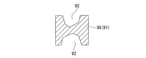
- the etching process by wet etching has a characteristic of being affected by the crystal plane orientation of the wafer substrate. Therefore, in the conventional method in which the processing of the outer shape and the processing of the groove portion 92 are processed by wet etching, the side surface and the bottom surface of the etched groove portion 92 are not flat surfaces, and have an irregular shape as shown in FIG. As a result, in-plane variation increases. Further, since the outer shape is also processed by wet etching, not only the groove portion 92 but also the side surfaces of the vibrating arm portions 90 and 91 and the base portion are not flat and become distorted. Therefore, the groove 92 having a desired shape cannot be accurately formed in the piezoelectric vibrating piece 95. Depending on the degree of in-plane variation, additional etching may be necessary.
- the excitation electrodes 93 and 94 when the excitation electrodes 93 and 94 are formed in the state of the groove 92 as shown in FIG. 28, the excitation electrodes 93 and 94 do not reliably face each other, and as a result, the CI value is a value as designed. I can't. In addition, each electrode may be short-circuited. For these reasons, it is difficult to achieve high quality and high performance.
- a protective film is generally formed in a region other than the region to be etched on the wafer substrate surface, and then the wafer substrate is dry etched and processed into a desired shape.
- a film of a hard metal element such as Ti, Ni, or Cr is adopted as the protective film, and the film thickness of the protective film It is necessary to thicken.
- the present invention has been made in view of the above circumstances, and a method for manufacturing a piezoelectric vibrating piece capable of forming a desired groove in a vibrating arm by dry etching, a piezoelectric vibrator having the piezoelectric vibrating piece, Furthermore, an oscillator, an electronic device, and a radio timepiece having the piezoelectric vibrator are provided.
- a method of manufacturing a piezoelectric vibrating piece according to the present invention includes a pair of vibrating arm portions arranged in parallel, a base portion that integrally fixes a base end side of the pair of vibrating arm portions, and a pair of the vibrating arm portions.
- Multiple protective film forming steps It is characterized by performing.
- a protective film is formed in a region other than the position corresponding to the groove portion in the wafer, and then dry etching is performed, so that both surfaces of the wafer are affected by the crystal plane orientation. It is possible to form a groove portion having no desired shape.
- the protective film forming step the first protective film forming step and the second protective film forming step are alternately repeated, and the protective film is alternately formed on both surfaces of the wafer by a predetermined thickness to obtain a desired film thickness. Therefore, it is possible to prevent the wafer from being warped when the protective film is formed on the wafer.
- the predetermined thickness is a thin film that does not warp even when a protective film is formed on the wafer.
- the protective film having the predetermined thickness is alternately formed on both sides of the wafer.
- the protective film is formed while canceling out the stress generated on both surfaces of the wafer when the protective film is formed. Accordingly, since the wafer does not warp when the protective film is formed, a desired groove can be formed by dry etching the wafer.
- the groove portion can be processed with high accuracy, and the side surface and the bottom surface of the groove portion can be made flat instead of an irregular shape. Therefore, the excitation electrode can be formed on the outer surface of the piezoelectric vibrating piece as designed, and the CI value can be made lower than that manufactured by the conventional method. Therefore, high quality and high performance can be achieved.
- the piezoelectric vibrating piece manufacturing method includes a pair of vibrating arm portions arranged in parallel, a base portion that integrally fixes a base end side of the pair of vibrating arm portions, and the pair of vibrating arms.
- a protective film is formed in a region other than the position corresponding to the groove portion in the wafer, and then dry etching is performed, so that both surfaces of the wafer are affected by the crystal plane orientation. It is possible to form a groove portion having no desired shape.
- the protective film is formed on both surfaces of the wafer at the same time in the protective film forming step, it is possible to prevent the wafer from warping when the protective film is formed on the wafer. That is, by forming the protective film on both surfaces of the wafer at the same time, the protective film is formed while canceling the stress generated on both surfaces of the wafer when the protective film is formed. Accordingly, since the wafer does not warp when the protective film is formed, a desired groove can be formed by dry etching the wafer.
- the groove portion can be processed with high accuracy, and the side surface and the bottom surface of the groove portion can be made flat instead of an irregular shape. Therefore, the excitation electrode can be formed on the outer surface of the piezoelectric vibrating piece as designed, and the CI value can be made lower than that manufactured by the conventional method. Therefore, high quality and high performance can be achieved.
- the piezoelectric vibrator according to the present invention is characterized by including the piezoelectric vibrating piece manufactured by the manufacturing method of the present invention.
- the groove portion has the piezoelectric vibrating piece precisely processed by dry etching, the quality of the piezoelectric vibrator can be improved.
- the excitation electrode formed on the outer surface of the piezoelectric vibrating piece (the outer surface including the groove) is also formed with high accuracy. Therefore, the CI value can be made lower than that of the conventional one, and the performance of the piezoelectric vibrator can be improved. Examples of such a piezoelectric vibrator include a cylinder package type piezoelectric vibrator and a box-type ceramic package type piezoelectric vibrator.
- An oscillator according to the present invention is characterized in that the piezoelectric vibrator of the present invention is electrically connected to an integrated circuit as an oscillator.
- an electronic apparatus according to the present invention is characterized in that the piezoelectric vibrator of the present invention is electrically connected to a timer unit.
- a radio timepiece according to the present invention is characterized in that the piezoelectric vibrator of the present invention is electrically connected to a filter portion.
- the oscillator, electronic device, and radio timepiece according to the present invention have the above-described piezoelectric vibrator, high quality and high performance can be achieved in the same manner.
- the protective film is alternately formed on both surfaces of the wafer by a predetermined thickness so as to have a desired film thickness.
- the predetermined thickness is a thin film that does not warp even when a protective film is formed on the wafer.
- the protective film having the predetermined thickness is alternately formed on both sides of the wafer. As a result, the protective film is formed while canceling out the stress generated on both surfaces of the wafer when the protective film is formed. Accordingly, since the wafer does not warp when the protective film is formed, a desired groove can be formed by dry etching the wafer.
- FIG. 1 is a view showing a first embodiment of a piezoelectric vibrating piece according to the present invention, and is a view of the piezoelectric vibrating piece as seen from above.
- FIG. 2 is a view of the piezoelectric vibrating piece shown in FIG. 1 as viewed from below.
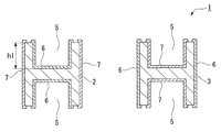
- FIG. 3 is a cross-sectional view taken along line AA shown in FIG.
- FIG. 4 is a perspective view of a state where an electrode portion is removed from the piezoelectric vibrating piece shown in FIG.
- FIG. 5 is a flowchart of the manufacturing method of the piezoelectric vibrating piece shown in FIG.
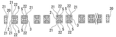
- FIG. 6 is a process diagram of the flowchart shown in FIG. 5 and shows a state in which an etching protective film is formed on both surfaces of the wafer.
- FIG. 7 is a partial cross-sectional view (1) showing a step of forming an etching protective film.
- FIG. 8 is a partial cross-sectional view (2) showing the step of forming an etching protective film.
- FIG. 9 is a partial cross-sectional view (3) showing the step of forming an etching protective film.
- FIG. 10 is a view showing a state after the etching protection film is patterned from the state shown in FIG. 6, and is a view of the wafer as viewed from above.
- FIG. 11 is a diagram showing a state after the etching protection film is patterned from the state shown in FIG.
- FIG. 12 is a diagram showing a state where the wafer is etched by dry etching from the state shown in FIG.
- FIG. 13 is a diagram showing a state in which another etching protective film is formed on both surfaces of the wafer from the state shown in FIG.
- FIG. 14 is a diagram showing a state after patterning an etching protective film formed later from the state shown in FIG.
- FIG. 15 is a diagram showing a state where the wafer is etched by wet etching from the state shown in FIG. 14 using two etching protective films as masks.
- FIG. 16 is a diagram showing a state in which a pair of vibrating arm portions having grooves are formed by removing two etching protective films from the state shown in FIG. FIG.
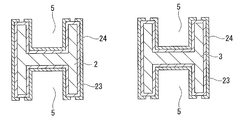
- FIG. 17 is a view showing a state where a predetermined position of the photoresist film is exposed after forming a conductive film and a photoresist film on the outer surfaces of the pair of vibrating arms from the state shown in FIG. is there.
- FIG. 18 is a view showing a state where the exposed photoresist film is developed from the state shown in FIG.
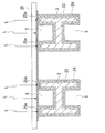
- FIG. 19 is a front view of a jig used for sputtering in the second embodiment of the present invention.
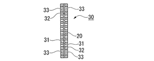
- 20 is a cross-sectional view taken along line BB in FIG.
- FIG. 21 is a view showing an embodiment of a cylinder type package type piezoelectric vibrator having a piezoelectric vibrating piece according to the present invention.
- FIG. 22 is a cross-sectional view showing an embodiment of a ceramic package type piezoelectric vibrator having a piezoelectric vibrating piece according to the present invention.
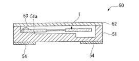
- 23 is a cross-sectional view taken along the section line CC shown in FIG.
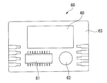
- FIG. 24 is a configuration diagram showing an embodiment of an oscillator having a piezoelectric vibrator according to the present invention.
- FIG. 25 is a configuration diagram showing an embodiment of an electronic apparatus having a piezoelectric vibrator according to the present invention.
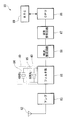
- FIG. 26 is a configuration diagram showing an embodiment of a radio timepiece having a piezoelectric vibrator according to the present invention.
- FIG. 27 is a cross-sectional view of a pair of vibrating arms having a conventional groove.
- FIG. 28 is a cross-sectional view of a conventional piezoelectric vibrating piece in which the groove has an irregular shape by wet etching.
- the piezoelectric vibrating reed 1 integrally forms a pair of vibrating arm portions 2 and 3 arranged in parallel and a base end side of the pair of vibrating arm portions 2 and 3.
- a pair of vibrating arms formed on the outer surface of the pair of vibrating arms 2 and 3 including the groove 5.
- An excitation electrode 8 including a first excitation electrode 6 and a second excitation electrode 7 for vibrating the portions 2 and 3, and mount electrodes 9 and 10 electrically connected to the excitation electrodes 6 and 7. Yes.
- the groove portion 5 is formed along the longitudinal direction X of the pair of vibrating arm portions 2 and 3, and is formed from the base 4 side of the vibrating arm portions 2 and 3 to approximately the middle. ing. In FIG. 4, the electrodes are not shown.
- the excitation electrode 8 including the first excitation electrode 6 and the second excitation electrode 7 is an electrode that vibrates the pair of vibrating arms 2 and 3 at a predetermined resonance frequency in a direction approaching or separating from each other. It is formed by patterning on the outer surfaces of the vibrating arms 2 and 3 while being electrically separated from each other. Specifically, as shown in FIG. 3, the first excitation electrode 6 is mainly formed on the groove portion 5 of one vibration arm portion 2 and on both side surfaces of the other vibration arm portion 3. Two excitation electrodes 7 are mainly formed on both side surfaces of one vibrating arm portion 2 and on a groove portion 5 of the other vibrating arm portion 3.
- the first excitation electrode 6 and the second excitation electrode 7 are electrically connected to the mount electrodes 9 and 10 via the extraction electrodes 11 and 12, respectively, on both surfaces of the base portion 4. It is connected to the.
- the piezoelectric vibrating reed 1 is applied with a voltage via the mount electrodes 9 and 10.
- the excitation electrode 8, the mount electrodes 9, 10 and the extraction electrodes 11, 12 are formed of a coating of a conductive film such as chromium (Cr), nickel (Ni), aluminum (Al), titanium (Ti), or the like. It is a thing.
- a weight metal film 13 for adjusting (frequency adjustment) the vibration state of itself within a predetermined frequency range is coated on the tips of the pair of vibrating arm portions 2 and 3.
- the weight metal film 13 is divided into a coarse adjustment film 13a used when the frequency is coarsely adjusted and a fine adjustment film 13b used when the frequency is finely adjusted.
- the piezoelectric vibrating reed 1 configured as described above is manufactured from a wafer 20 made of a piezoelectric material such as crystal, lithium tantalate or lithium niobate, as shown in FIG. At this time, the groove 5 is produced by etching the wafer 20 by dry etching. This manufacturing method will be described in detail later. Further, the pair of vibrating arm portions 2 and 3 and the base portion 4 are manufactured by sequentially performing two etching processes on the wafer 20 which are different from each other in dry etching and wet etching.
- the width W is about 0.5 mm to 0.6 mm
- the total length L is about 2.0 mm to 3.2 mm
- the thickness T is about 0.10 mm.
- the depth h1 (see FIG. 3) of the groove 5 is about 40 ⁇ m.
- Each electrode such as the excitation electrode 8 is, for example, a laminated film of chromium (Cr) and gold (Au) when the wafer 20 is a crystal, and a chromium film having good adhesion to the crystal is used as a base. After the film formation, a gold thin film is applied to the surface.
- the present invention is not limited to this, and for example, a gold thin film may be further laminated on the surface of a laminated film of chromium and nichrome (NiCr).
- a predetermined drive voltage is applied to the mount electrodes 9 and 10.
- a current can be passed to the excitation electrode 8 composed of the first excitation electrode 6 and the second excitation electrode 7 via the extraction electrodes 11 and 12, and the pair of vibrating arm portions 2 and 3 can be brought close to each other. It can be vibrated at a predetermined frequency in the direction of separation.
- the vibration of the pair of vibrating arm portions 2 and 3 can be used as a time source, a control signal timing source, a reference signal source, and the like.
- the manufacturing method according to the present embodiment performs a protective film forming step, a patterning step, a first etching step, a protective step, a second etching step, and a removing step in order, from the wafer 20 at a time.
- This is a method for producing a plurality of piezoelectric vibrating reeds 1. Each of these steps will be described in detail below.
- a wafer 20 is prepared.
- an etching protective film 21 that protects the wafer 20 during etching is formed on both surfaces of the wafer 20 by sputtering or the like (protective film forming step).
- the etching protection film 21 for example, titanium (Ti) is formed to a thickness of about 3 ⁇ m.
- the etching protective film 21 having a thickness of about 3 ⁇ m is formed on both surfaces of the wafer 20, respectively.
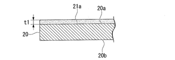
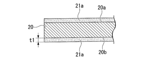
- the protective film 21a is formed by the predetermined thickness t1
- the wafer 20 disposed in the sputtering apparatus may be inverted every predetermined time and formed while changing the film formation surface. Good.
- the etching protective film 21 is patterned into the outer shape of the piezoelectric vibrating reed 1 with the groove portion 5 being open (patterning step). Specifically, first, a photoresist film (not shown) is patterned on the etching protection film 21 by a photolithography technique. At this time, patterning is performed so as to surround the periphery of the groove 5 and the piezoelectric vibrating piece 1. Then, etching is performed using this photoresist film as a mask, and the unmasked etching protection film 21 is selectively removed. Then, the photoresist film is removed after the etching process.
- the etching protective film 21 can be patterned in the shape mentioned above. That is, patterning can be performed along the outer shape of the piezoelectric vibrating piece 1, that is, the outer shapes of the pair of vibrating arm portions 2 and 3 and the base portion 4 with the groove portion 5 being open. At this time, the patterning is performed by the number of the plurality of piezoelectric vibrating reeds 1.
- both surfaces of the wafer 20 are etched by dry etching with a fluorine-based gas using the patterned etching protective film 21 as a mask (first etching process).
- the wafer 20 is etched by the depth h 1 of the groove 5.
- the groove portions 5 can be formed on both surfaces of the wafer 20, and the region not masked by the etching protection film 21 is removed from the surface by the depth h1 of the groove portions 5, thereby The outer shape of the resonator element 1 can be formed by the depth h1 of the groove 5.
- the groove portion 5 can be accurately removed by the depth h1.
- an etching protection film 22 that protects the wafer 20 during the etching process is formed only in the groove portion 5 in the exposed portion (protection step).
- an etching protection film 22 is formed on each side of the wafer 20.
- the etching protective film 22 is, for example, a resin-based photoresist film, and is formed by spray coating or a combination of spray coating and spin coating. At this time, in this embodiment, not only the wafer 20 but also the etching protective film 22 is formed until the previously formed etching protective film 21 is completely hidden.
- the formed etching protective film 22 is patterned by a photolithography technique using a photoresist film (not shown) in the same manner as the patterning of the etching protective film 21, so that the grooves 5 are formed as shown in FIG. Leave only in the part.
- the wafer 20 is in a state where only the area surrounding the periphery of the piezoelectric vibrating piece 1 is exposed.
- the etching protective film 22 is once formed on the entire surface of the wafer 20 and then patterned to form the etching protective film 22 only in the groove 5.
- the present invention is not limited to this case.
- the etching protective film 22 may be formed through the mask. Even in this case, the etching protective film 22 can be formed only in the groove 5. In any case, any method may be used as long as the etching protective film 22 can be formed only in the groove 5.
- the wafer 20 is etched by wet etching with hydrofluoric acid or the like using the etching protective film 21 formed first and the etching protective film 22 formed later as a mask (second etching process).
- the remaining portion of the wafer 20 etched from the surface by the depth h1 of the groove 5 in the first etching process is completely removed. That is, both surfaces of the wafer 20 are penetrated. Accordingly, as shown in FIG. 15, the pair of vibrating arm portions 2, 3 and the base portion 4 can be completely formed, and the pair of vibrating arm portions 2, 3 are integrally fixed to the base portion 4.
- Piece 1 can be obtained.
- the etching protection films 21 and 22 are finally removed (removal process). Accordingly, the piezoelectric vibrating piece 1 shown in FIG. 4 in which the groove portions 5 are formed on both surfaces of the pair of vibrating arm portions 2 and 3 can be manufactured.
- the excitation electrode 8, the extraction electrodes 11, 12 and the mount electrodes 9, 10 are formed (electrode formation step). Specifically, as shown in FIG. 17, a conductive film 23 to be the excitation electrode 8, the extraction electrodes 11 and 12, and the mount electrodes 9 and 10 is formed on the outer surface of the piezoelectric vibrating piece 1. A positive photoresist film 24 is formed on the conductive film 23. Next, the photomask 25 in which the opening 25 a having a predetermined size is formed is positioned on the photoresist film 24. At this time, the photomask 25 is accurately positioned so that the opening 25a is positioned on each of the vibrating arms 2 and 3 with the groove 5 interposed therebetween. Next, the parallel light L is irradiated from above the photomask 25, and the photoresist film 24 is exposed through the opening 25a. At this time, the photoresist film 24 is exposed only to the region where the opening 25a is formed.
- the photoresist film 24 is developed. Thereby, as shown in FIG. 18, the photoresist film 24 is in a state where only the exposed region is removed. Then, after etching the conductive film 23 using the photoresist film 24 as a mask, the photoresist film 24 is removed. Thereby, as shown in FIG. 3, two excitation electrodes 8 having different polarities can be formed on the outer surfaces of the vibrating arm portions 2 and 3 including the groove portion 5. Further, the extraction electrodes 11 and 12, the mount electrodes 9 and 10, and the weight metal film 13 can also be formed from the conductive film 23 at the same timing. As a result, the piezoelectric vibrating piece 1 shown in FIGS. 1 to 3 can be manufactured.
- the influence of the crystal plane orientation on both surfaces of the wafer 20 is performed by dry etching. It is possible to form a groove portion 5 having a desired shape that is not subjected to the above. Further, since the protective film 21a having the predetermined thickness t1 is alternately formed on both surfaces of the wafer 20 so as to become the etching protective film 21 having a desired film thickness, it is possible to prevent the wafer 20 from warping. be able to. That is, the predetermined thickness t1 is a thin film (protective film 21a) that does not warp even when the wafer 20 is formed.
- the protective film 21a having the predetermined thickness t1 is applied to both surfaces of the wafer 20.
- the etching protective film 21 is formed while canceling stresses generated on both surfaces of the wafer 20 when the protective film is formed. Accordingly, since the wafer 20 is not warped during the formation of the protective film, the desired groove 5 can be formed by dry etching the wafer 20.
- the groove portion 5 can be processed with high accuracy, and the side surface and the bottom surface of the groove portion 5 can be made flat instead of an irregular shape. Therefore, the excitation electrode 8 can be formed on the outer surface of the piezoelectric vibrating piece 1 as designed, and the CI value can be made lower than that manufactured by the conventional method.
- the positional relationship can be made to be more accurately opposed than the conventional one. Therefore, the CI value can be made lower than that manufactured by the conventional method. Therefore, high quality and high performance can be achieved.
- the wafer 20 is prepared (S1).
- an etching protection film 21 that protects the wafer 20 during etching is formed on both surfaces of the wafer 20 by sputtering or the like (S2).
- the etching protection film 21 for example, titanium (Ti) is formed to a thickness of about 3 ⁇ m.
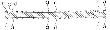
- the etching protective film 21 is formed on both surfaces of the wafer 20 at the same time so as to have a desired film thickness. That is, if the etching protection film 21 is formed on the one surface 20a and the other surface 20b of the wafer 20 at the same time, it is possible to prevent the wafer 20 from warping.
- openings are formed in regions where the etching protection film 21 is formed on both surfaces of the wafer 20.
- a jig 30 having 31 is used.
- the jig 30 includes a pair of plate materials 32 and 32, and an opening 31 is appropriately formed in the plate material 32.
- the wafer 20 can be interposed between the pair of plate members 32, 32.
- Fixing magnets 33 are provided at the four corners of the pair of plate members 32 and 32, and positioning pins 34 are provided for positioning the wafer 20 when the wafer 20 is placed on the jig 30.
- the etching protective film 21 can be simultaneously formed on both surfaces of the wafer 20.
- the etching protection film 21 is formed on both surfaces of the wafer 20 at the same time, it is possible to prevent the wafer 20 from warping when the etching protection film 21 is formed on the wafer 20. it can. That is, by simultaneously forming the etching protective film 21 on both surfaces of the wafer 20, the etching protective film 21 is formed while canceling the stress generated on both surfaces of the wafer 20. Accordingly, since the wafer 20 is not warped when the etching protective film 21 is formed, the desired groove 5 can be formed by dry etching the wafer 20.
- the groove portion 5 can be processed with high accuracy, and the side surface and the bottom surface of the groove portion 5 can be made flat instead of an irregular shape. Therefore, the excitation electrode 8 can be formed on the outer surface of the piezoelectric vibrating piece 1 as designed, and the CI value can be made lower than that manufactured by the conventional method. Therefore, high quality and high performance can be achieved.
- the piezoelectric vibrator 40 of the present embodiment includes a piezoelectric vibrating piece 1, an airtight terminal 41, and a case 42 joined to the airtight terminal 41 with the piezoelectric vibrating piece 1 sealed inside. It has.
- the airtight terminal 41 includes an annular stem 43 and two leads 44 that are disposed so as to penetrate the stem 43 and are electrically and physically connected to both the mount electrodes 9 and 10 of the piezoelectric vibrating piece 1.
- the lead 44 and the stem 43 are integrally fixed in an insulated state, and at the same time, a filler 45 that seals the inside of the case 42 is formed.
- the stem 43 is formed of a metal material (for example, low carbon steel (Fe), iron nickel alloy (Fe—Ni), iron nickel cobalt alloy (Fe—Ni—Co)) in an annular shape.
- the outer periphery of the stem 43 is coated with a metal film (not shown) such as heat-resistant solder plating, tin-copper alloy or gold-tin alloy.
- the material of the filler 45 is, for example, borosilicate glass.
- a portion protruding into the case 42 is an inner lead 44a, and a portion protruding outside the case 42 is an outer lead 44b.
- the outer lead 44b functions as an external connection terminal.
- the case 42 is press-fitted into the outer periphery of the stem 43 and is fixedly fitted. Specifically, the case 42 and the stem 43 are fixed by cold welding with a metal film coated on the outer periphery of the stem 43 interposed. Since the press-fitting of the case 42 is performed in a vacuum atmosphere, the space surrounding the piezoelectric vibrating reed 1 in the case 42 is hermetically sealed in a vacuum state.
- the piezoelectric vibrator 40 since the piezoelectric vibrator piece 1 with higher quality and higher performance is provided, the piezoelectric vibrator 40 itself is also improved in quality and High performance can be achieved. In particular, since the inside of the case 42 can be evacuated, the vibration efficiency of the pair of vibrating arm portions 2 and 3 can be improved.
- piezoelectric vibrator Next, another example of the piezoelectric vibrator having the piezoelectric vibrating piece 1 according to the present invention will be described with reference to FIGS.
- a piezoelectric vibrator a ceramic package type piezoelectric vibrator 50 in which the piezoelectric vibrating piece 1 is fixed in a box with a lid will be described as an example.
- the piezoelectric vibrator 50 includes a piezoelectric vibrating piece 1, a base 51, and a lid 52 made of metal or glass.
- the base portion 4 of the piezoelectric vibrating piece 1 is fixed and fixed to the joint portion 51 a of the base 51 with a conductive adhesive 53.
- the base 51 is hermetically sealed with a lid 52 serving as a lid using various means such as electron beam welding, vacuum seam welding, or joining with low melting point glass or eutectic metal in vacuum.
- the mount electrodes 9 and 10 formed on the base portion 4 of the piezoelectric vibrating reed 1 are electrically connected to the external electrode 54 outside the base 51 by an internal connection (not shown) through the joint portion 51a.
- the ceramic package type piezoelectric vibrator 50 configured as described above also has the piezoelectric vibrator element 1 with higher quality and higher performance, and therefore the piezoelectric vibrator 50 itself is also improved in quality and higher quality. Performance can be improved.
- the space surrounded by the base 51 and the lid 52 can be in a vacuum state, the vibration efficiency of the pair of vibrating arm portions 2 and 3 can be improved similarly.
- an oscillator 60 including the piezoelectric vibrator 40 having the piezoelectric vibrating piece 1 will be described as an example.
- the oscillator 60 according to the present embodiment is configured such that the piezoelectric vibrator 40 is an oscillator electrically connected to an integrated circuit 61.
- the oscillator 60 includes a substrate 63 on which an electronic component 62 such as a capacitor is mounted.
- the integrated circuit 61 for the oscillator 60 is mounted on the substrate 63, and the piezoelectric vibrating piece 1 of the piezoelectric vibrator 40 is mounted in the vicinity of the integrated circuit 61.
- the electronic component 62, the integrated circuit 61, and the piezoelectric vibrator 40 are electrically connected by a wiring pattern (not shown). Each component is molded with a resin (not shown).
- the piezoelectric vibrating reed 1 in the piezoelectric vibrator 40 vibrates. This vibration is converted into an electric signal by the piezoelectric characteristics of the piezoelectric vibrating piece 1 and input to the integrated circuit 61 as an electric signal. The input electrical signal is subjected to various processes by the integrated circuit 61 and output as a frequency signal. Thereby, the piezoelectric vibrator 40 functions as an oscillator.
- the piezoelectric vibrator 40 with high quality and high performance is provided, the quality and performance of the oscillator 60 itself can be improved. Reliability can be improved. In addition to this, it is possible to obtain a highly accurate frequency signal that is stable over a long period of time.
- a portable information device 70 including the piezoelectric vibrator 40 having the piezoelectric vibrating piece 1 will be described as an example of the electronic device.
- the portable information device 70 of this embodiment is typified by, for example, a mobile phone, and is a development and improvement of a wrist watch in the prior art. The appearance is similar to that of a wristwatch, and a liquid crystal display is arranged in a portion corresponding to a dial so that the current time and the like can be displayed on this screen.
- the portable information device 70 includes a piezoelectric vibrator 40 and a power supply unit 71 for supplying power.
- the power supply unit 71 is made of, for example, a lithium secondary battery.
- the power supply unit 71 includes a control unit 72 that performs various controls, a clock unit 73 that counts time, a communication unit 74 that communicates with the outside, a display unit 75 that displays various information, and the like.
- a voltage detection unit 76 that detects the voltage of the functional unit is connected in parallel. Power is supplied to each functional unit by the power supply unit 71.
- the control unit 72 controls the operation of the entire system such as transmission and reception of voice data, measurement and display of the current time by controlling each functional unit.
- the control unit 72 includes a ROM in which a program is written in advance, a CPU that reads and executes the program written in the ROM, and a RAM that is used as a work area of the CPU.
- the timer unit 73 includes an integrated circuit including an oscillation circuit, a register circuit, a counter circuit, an interface circuit, and the like, and the piezoelectric vibrator 40.
- the piezoelectric vibrator 40 When a voltage is applied to the piezoelectric vibrator 40, the piezoelectric vibrating piece 1 vibrates, and the vibration is converted into an electric signal by the piezoelectric characteristics of the crystal and is input to the oscillation circuit as an electric signal.
- the output of the oscillation circuit is binarized and counted by a register circuit and a counter circuit. Then, signals are transmitted to and received from the control unit 72 via the interface circuit, and the display unit 75 displays the current time, the current date, calendar information, and the like.
- the communication unit 74 has the same functions as a conventional mobile phone, and includes a radio unit 77, a voice processing unit 78, a switching unit 79, an amplification unit 80, a voice input / output unit 81, a telephone number input unit 82, and a ring tone generation unit. 83 and a call control memory unit 84.
- the wireless unit 77 exchanges various data such as audio data with the base station via the antenna 85.
- the audio processing unit 78 encodes and decodes the audio signal input from the radio unit 77 or the amplification unit 80.
- the amplifying unit 80 amplifies the signal input from the audio processing unit 78 or the audio input / output unit 81 to a predetermined level.
- the voice input / output unit 81 includes a speaker, a microphone, and the like, and amplifies a ringtone and a received voice or collects a voice.
- the ring tone generator 83 generates a ring tone in response to a call from the base station.
- the switching unit 79 switches the amplifying unit 80 connected to the voice processing unit 78 to the ringing tone generating unit 83 only when an incoming call is received, so that the ringing tone generated by the ringing tone generating unit 83 passes through the amplifying unit 80.
- the call control memory unit 84 stores a program related to incoming / outgoing call control of communication.
- the telephone number input unit 82 includes, for example, a number key from 0 to 9 and other keys, and the telephone number of the call destination is input by pressing these number keys.
- the voltage detection unit 76 detects the voltage drop and notifies the control unit 72 of the voltage drop.
- the predetermined voltage value at this time is a value set in advance as a minimum voltage necessary for stably operating the communication unit 74, and is, for example, about 3V.
- the control unit 72 prohibits the operations of the radio unit 77, the voice processing unit 78, the switching unit 79, and the ring tone generation unit 83. In particular, it is essential to stop the operation of the wireless unit 77 with high power consumption. Further, the display unit 75 displays that the communication unit 74 has become unusable due to insufficient battery power.
- the operation of the communication unit 74 can be prohibited by the voltage detection unit 76 and the control unit 72, and that effect can be displayed on the display unit 75.
- This display may be a text message, but as a more intuitive display, a x (X) mark may be attached to the telephone icon displayed at the top of the display surface of the display unit 75.
- the function of the communication part 74 can be more reliably stopped by providing the power supply cutoff part 86 which can selectively interrupt the power supply of the part which concerns on the function of the communication part 74.
- the portable information device 70 of the present embodiment since the piezoelectric vibrator 40 with high quality and high performance is provided, it is possible to improve the quality and performance of the portable information device 70 itself. And the reliability of the product can be improved. In addition to this, it is possible to display highly accurate clock information that is stable over a long period of time.
- the radio timepiece 80 of the present embodiment includes a piezoelectric vibrator 40 electrically connected to a filter unit 81, and receives a standard radio wave including timepiece information to accurately It is a clock with a function of automatically correcting and displaying the correct time.
- a standard radio wave including timepiece information to accurately It is a clock with a function of automatically correcting and displaying the correct time.
- transmitting stations transmit standard radio waves in Fukushima Prefecture (40 kHz) and Saga Prefecture (60 kHz), each transmitting standard radio waves.
- Long waves such as 40 kHz or 60 kHz have the property of propagating the surface of the earth and the property of propagating while reflecting the ionosphere and the surface of the earth, so the propagation range is wide, and the above two transmitting stations cover all of Japan. is doing.
- the antenna 82 receives a long standard wave of 40 kHz or 60 kHz.
- the long-wave standard radio wave is obtained by subjecting time information called a time code to AM modulation on a 40 kHz or 60 kHz carrier wave.
- the received long standard wave is amplified by the amplifier 83 and filtered and tuned by the filter unit 81 having the plurality of piezoelectric vibrators 40.
- the piezoelectric vibrator 40 in the present embodiment includes crystal vibrator portions 84 and 85 having resonance frequencies of 40 kHz and 60 kHz that are the same as the carrier frequency, respectively.
- the filtered signal having a predetermined frequency is detected and demodulated by a detection and rectification circuit 86.
- the time code is taken out via the waveform shaping circuit 87 and counted by the CPU 88.
- the CPU 88 reads information such as the current year, accumulated date, day of the week, and time. The read information is reflected in the RTC 89, and accurate time information is displayed. Since the carrier wave is 40 kHz or 60 kHz, the crystal vibrator portions 84 and 85 are preferably vibrators having the tuning fork type structure described above.
- the frequency of the long standard radio wave is different overseas.
- a standard radio wave of 77.5 KHz is used. Therefore, when the radio timepiece 80 that can be used overseas is incorporated in a portable device, the piezoelectric vibrator 40 having a frequency different from that in Japan is required.
- the piezoelectric vibrator 40 with high quality and high performance is provided, it is possible to improve the quality and performance of the radio timepiece 80 itself. Product reliability can be improved. In addition to this, it is possible to count time stably and with high accuracy over a long period of time.
- the step of forming the groove portion is not the method described above, but a mask member such as a polyimide tape is attached to the region where the groove portion is formed, and then the entire surface of the wafer is sputtered.
- You may form by dry etching. That is, after exposing a position corresponding to the groove portion on the wafer, the groove portion may be formed by dry etching.
- the method for manufacturing a piezoelectric vibrating piece according to the present invention can be applied to a piezoelectric vibrating piece in which a groove portion is formed in a vibrating arm portion.
Landscapes
- Physics & Mathematics (AREA)
- Acoustics & Sound (AREA)
- Chemical & Material Sciences (AREA)
- Crystallography & Structural Chemistry (AREA)
- Engineering & Computer Science (AREA)
- Manufacturing & Machinery (AREA)
- Piezo-Electric Or Mechanical Vibrators, Or Delay Or Filter Circuits (AREA)
- Oscillators With Electromechanical Resonators (AREA)
Abstract
Description
この圧電振動子は、搭載される機器の小型化に伴って、今後さらなる小型化が望まれている。小型化を図る方法としては、いくつかの方法が考えられているが、その1つとして振動腕部の両面に溝部を形成した音叉型の圧電振動片を利用する方法がある。
通常、この音叉型の圧電振動片は、互いに平行に配置され、基端側が基部に一体的に固定された一対の振動腕部と、前記一対の振動腕部の外表面上(溝部を含む)に形成されて一対の振動腕部を振動させる励振電極と、を有している。
初めに、ウェットエッチングによるエッチング加工は、ウエハ基板の結晶の面方位の影響を受けてしまう特性を有している。そのため、外形形状の加工と溝部92の加工とをウェットエッチングにより加工する従来の方法では、エッチングされた溝部92の側面や底面が平坦面にならず、図28に示すようにいびつな形状になってしまい、面内ばらつきが大きくなる。また、外形形状もウェットエッチングで加工しているため、溝部92だけでなく振動腕部90、91や基部の側面も平坦面にならず、いびつな形状になる。そのため、圧電振動片95に所望の形状の溝部92を精度良く形成することができない。また、面内ばらつきの程度によっては、追加エッチングが必要な場合もある。
ドライエッチングを行う際には、一般的にウエハ基板面におけるエッチングを行う領域以外に保護膜を形成した後に、ウエハ基板をドライエッチングして所望の形状に加工する。ここで、ウエハ基板に溝部92を形成するには、ウエハ基板を深堀する必要があるため、Ti、NiまたはCrなどの硬い金属元素の膜を保護膜として採用し、かつ、保護膜の膜厚を厚くする必要がある。しかしながら、硬い金属元素の膜は、応力が大きいため、保護膜の膜厚を厚くすると、ウエハ基板の反りが発生するという問題がある。つまり、ウエハ基板が反った状態でドライエッチングをしても所望の溝部92を形成することができない虞がある。
本発明に係る圧電振動片の製造方法は、平行に配置された一対の振動腕部と、前記一対の振動腕部の基端側を一体的に固定する基部と、前記一対の振動腕部の両面に前記振動腕部の長手方向に沿ってそれぞれ形成された溝部と、を備えた圧電振動片をウエハから製造する圧電振動片の製造方法であって、前記ウエハにおける前記溝部に対応する位置以外の領域に保護膜を形成する保護膜形成工程と、前記保護膜をマスクとして前記ウエハに対してドライエッチングを行うことにより前記溝部を形成する溝部形成工程と、を有し、前記保護膜形成工程では、前記ウエハの第一面に対して所定厚さの前記保護膜を形成する第一保護膜形成工程と、前記ウエハの第二面に対して所定厚さの前記保護膜を形成する第二保護膜形成工程とを、交互に複数回行うことを特徴としている。
ここで、保護膜形成工程において、第一保護膜形成工程と第二保護膜形成工程とを交互に繰り返し、保護膜を所定厚さずつウエハの両面に対して交互に形成して所望の膜厚になるように構成したため、ウエハに保護膜を形成する際にウエハに反りが発生するのを防止することができる。つまり、所定厚さとは、ウエハに保護膜を成膜しても反りが発生しない程度の薄い膜のことであり、この所定厚さの保護膜をウエハの両面に対して交互に成膜することにより、保護膜形成時にウエハ両面に生じる応力が打ち消しあいながら保護膜が形成される。したがって、保護膜形成時にウエハに反りが発生しないため、ウエハをドライエッチングすることにより、所望の溝部を形成することができる。
ここで、保護膜形成工程において、保護膜をウエハの両面に対して同時に形成するように構成したため、ウエハに保護膜を形成する際にウエハに反りが発生するのを防止することができる。つまり、保護膜をウエハの両面に対して同時に成膜することにより、保護膜形成時にウエハ両面に生じる応力が打ち消しあいながら保護膜が形成される。したがって、保護膜形成時にウエハに反りが発生しないため、ウエハをドライエッチングすることにより、所望の溝部を形成することができる。
また、本発明に係る電子機器は、上記本発明の圧電振動子が、計時部に電気的に接続されていることを特徴としている。
また、本発明に係る電波時計は、上記本発明の圧電振動子が、フィルタ部に電気的に接続されていることを特徴としている。
2 振動腕部
3 振動腕部
4 基部
5 溝部
8 励振電極
20 ウエハ
20a 一方の面(第一面)
20b 他方の面(第二面)
21 エッチング保護膜
22 エッチング保護膜
40 圧電振動子
50 圧電振動子
60 発振器
61 集積回路
70 電子機器(携帯情報機器)
73 計時部
80 電波時計
81 フィルタ部
以下、本発明に係る圧電振動片及び前記圧電振動片の製造方法の第1実施形態を、図1~図18を参照して説明する。
本実施形態の圧電振動片1は、図1から図3に示すように、平行に配置された一対の振動腕部2、3と、一対の振動腕部2、3の基端側を一体的に固定する基部4と、一対の振動腕部2、3の両面にそれぞれ形成された溝部5と、溝部5を含む一対の振動腕部2、3の外表面上に形成され、一対の振動腕部2、3を振動させる第1の励振電極6と第2の励振電極7とからなる励振電極8と、両励振電極6、7に電気的に接続されたマウント電極9、10とを備えている。
なお、励振電極8、マウント電極9、10及び引き出し電極11、12は、例えば、クロム(Cr)、ニッケル(Ni)、アルミニウム(Al)やチタン(Ti)等の導電性膜の被膜により形成されたものである。
本実施形態の製造方法は、保護膜形成工程と、パターニング工程と、第1のエッチング工程と、保護工程と、第2のエッチング工程と、除去工程とを順番に行って、ウエハ20から一度に複数の圧電振動片1を製造する方法である。これら各工程について、以下に詳細に説明する。
なお、本実施形態では、一旦ウエハ20の全面にエッチング保護膜22を成膜した後、パターニングすることでエッチング保護膜22を溝部5だけに成膜したが、この場合に限られず、例えば溝部5の部分だけ開口した図示しないマスクをウエハ20に重ねた後、前記マスクを介してエッチング保護膜22を成膜しても構わない。この場合であっても、溝部5だけにエッチング保護膜22を成膜することができる。いずれにしても、溝部5だけにエッチング保護膜22を成膜できれば、その方法は何でも構わない。
また、所定厚さt1の保護膜21aをウエハ20の両面に対して交互に形成して所望の膜厚のエッチング保護膜21になるように構成したため、ウエハ20に反りが発生するのを防止することができる。つまり、所定厚さt1とは、ウエハ20成膜しても反りが発生しない程度の薄い膜(保護膜21a)のことであり、この所定厚さt1の保護膜21aをウエハ20の両面に対して交互に成膜することにより、保護膜形成時にウエハ20の両面に生じる応力が打ち消しあいながらエッチング保護膜21が形成される。したがって、保護膜形成時にウエハ20に反りが発生しないため、ウエハ20をドライエッチングすることにより、所望の溝部5を形成することができる。
次に、本発明に係る圧電振動片の製造方法の第2実施形態を、図19、図20を参照して説明する。なお、この第2実施形態においては、第1実施形態における構成要素と同一の部分については、同一の符号を付しその説明を省略する。
第2実施形態と第1実施形態とは、ウエハ20にエッチング保護膜21を成膜する成膜方法が異なるだけであり、その他の構成は略同一である。
本実施形態の圧電振動子40は、図21に示すように、圧電振動片1と、気密端子41と、圧電振動片1を内部に封止した状態で気密端子41に接合されたケース42とを備えている。
上記ステム43は、金属材料(例えば、低炭素鋼(Fe)、鉄ニッケル合金(Fe-Ni)、鉄ニッケルコバルト合金(Fe-Ni-Co))で環状に形成されたものである。
なお、ステム43の外周には、耐熱ハンダメッキや、錫銅合金や金錫合金等の図示しない金属膜が被膜されている。また、上記充填材45の材料としては、例えば、ホウ珪酸ガラスである。また、2本のリード44は、ケース42内に突出している部分がインナーリード44aとなり、ケース42外に突出している部分がアウターリード44bとなっている。そして、このアウターリード44bが、外部接続端子として機能するようになっている。
次に、本発明に係る圧電振動片1を有する圧電振動子の他の例について、図22及び図23を参照して説明する。なお、本実施形態では、圧電振動子として、圧電振動片1を蓋付きの箱の中に固定したセラミックパッケージタイプの圧電振動子50を例にして説明する。
次に、本発明に係る発振器の一実施形態について、図24を参照しながら説明する。なお、本実施形態では、圧電振動片1を有する圧電振動子40を備えた発振器60を例に挙げて説明する。
本実施形態の発振器60は、図24に示すように、圧電振動子40を、集積回路61に電気的に接続された発振子として構成したものである。この発振器60は、コンデンサ等の電子部品62が実装された基板63を備えている。基板63には、発振器60用の上記集積回路61が実装されており、この集積回路61の近傍に、圧電振動子40の圧電振動片1が実装されている。これら電子部品62、集積回路61及び圧電振動子40は、図示しない配線パターンによってそれぞれ電気的に接続されている。なお、各構成部品は、図示しない樹脂によりモールドされている。
また、集積回路61の構成を、例えば、RTC(リアルタイムクロック)モジュール等を要求に応じて選択的に設定することで、時計用単機能発振器60等の他、当該機器や外部機器の動作日や時刻を制御したり、時刻やカレンダー等を提供したりする機能を付加することができる。
次に、本発明に係る電子機器の一実施形態について、図25を参照して説明する。なお電子機器として、圧電振動片1を有する圧電振動子40を備えた携帯情報機器70を例に挙げて説明する。
初めに本実施形態の携帯情報機器70は、例えば、携帯電話に代表されるものであり、従来技術における腕時計を発展、改良したものである。外観は腕時計に類似し、文字盤に相当する部分に液晶ディスプレイを配し、この画面上に現在の時刻等を表示させることができるものである。また、通信機として利用する場合には、手首から外し、バンドの内側部分に内蔵されたスピーカ及びマイクロフォンによって、従来技術の携帯電話と同様の通信を行うことが可能である。しかしながら、従来の携帯電話と比較して、格段に小型化及び軽量化されている。
無線部77は、音声データ等の各種データを、アンテナ85を介して基地局と送受信のやりとりを行う。音声処理部78は、無線部77又は増幅部80から入力された音声信号を符号化及び複号化する。増幅部80は、音声処理部78又は音声入出力部81から入力された信号を、所定のレベルまで増幅する。音声入出力部81は、スピーカやマイクロフォン等からなり、着信音や受話音声を拡声したり、音声を集音したりする。
なお、呼制御メモリ部84は、通信の発着呼制御に係るプログラムを格納する。また、電話番号入力部82は、例えば、0から9の番号キー及びその他のキーを備えており、これら番号キー等を押下することにより、通話先の電話番号等が入力される。
このときの所定の電圧値は、通信部74を安定して動作させるために必要な最低限の電圧として予め設定されている値であり、例えば、3V程度となる。電圧検出部76から電圧降下の通知を受けた制御部72は、無線部77、音声処理部78、切替部79及び着信音発生部83の動作を禁止する。特に、消費電力の大きな無線部77の動作停止は、必須となる。更に、表示部75に、通信部74が電池残量の不足により使用不能になった旨が表示される。
なお、通信部74の機能に係る部分の電源を、選択的に遮断することができる電源遮断部86を備えることで、通信部74の機能をより確実に停止することができる。
次に、本発明に係る電波時計の一実施形態について、図26を参照して説明する。なお、本実施形態では、圧電振動片1を有する圧電振動子40を備えた電波時計を例に挙げて説明する。
本実施形態の電波時計80は、図26に示すように、フィルタ部81に電気的に接続された圧電振動子40を備えたものであり、時計情報を含む標準の電波を受信して、正確な時刻に自動修正して表示する機能を備えた時計である。
日本国内には、福島県(40kHz)と佐賀県(60kHz)とに、標準の電波を送信する送信所(送信局)があり、それぞれ標準電波を送信している。40kHz若しくは60kHzのような長波は、地表を伝播する性質と、電離層と地表とを反射しながら伝播する性質とを併せもつため、伝播範囲が広く、上述した2つの送信所で日本国内を全て網羅している。
アンテナ82は、40kHz若しくは60kHzの長波の標準電波を受信する。長波の標準電波は、タイムコードと呼ばれる時刻情報を、40kHz若しくは60kHzの搬送波にAM変調をかけたものである。受信された長波の標準電波は、アンプ83によって増幅され、複数の圧電振動子40を有するフィルタ部81によって濾波、同調される。
本実施形態における圧電振動子40は、上記搬送周波数と同一の40kHz及び60kHzの共振周波数を有する水晶振動子部84、85をそれぞれ備えている。
搬送波は、40kHz若しくは60kHzであるから、水晶振動子部84、85は、上述した音叉型の構造を持つ振動子が好適である。
例えば、溝部を形成する工程は、上述の方法ではなく、溝部を形成する領域にポリイミドテープなどのマスク部材を貼着した後に、ウエハ全面にスパッタを施し、その後、マスク部材を除去した後に溝部をドライエッチングにより形成してもよい。つまり、ウエハにおける溝部に相当する位置を露出させた後に、ドライエッチングにより溝部を形成すればよい。
Claims (6)
- 平行に配置された一対の振動腕部と、前記一対の振動腕部の基端側を一体的に固定する基部と、前記一対の振動腕部の両面に前記振動腕部の長手方向に沿ってそれぞれ形成された溝部と、を備えた圧電振動片をウエハから製造する圧電振動片の製造方法において、
前記ウエハにおける前記溝部に対応する位置以外の領域に保護膜を形成する保護膜形成工程と、
前記保護膜をマスクとして前記ウエハに対してドライエッチングを行うことにより前記溝部を形成する溝部形成工程と、を有し、
前記保護膜形成工程では、前記ウエハの第一面に対して所定厚さの前記保護膜を形成する第一保護膜形成工程と、前記ウエハの第二面に対して所定厚さの前記保護膜を形成する第二保護膜形成工程とを、交互に複数回行うことを特徴とする圧電振動片の製造方法。 - 平行に配置された一対の振動腕部と、前記一対の振動腕部の基端側を一体的に固定する基部と、前記一対の振動腕部の両面に振動腕部の長手方向に沿ってそれぞれ形成された溝部と、を備えた圧電振動片をウエハから製造する圧電振動片の製造方法において、
前記ウエハにおける前記溝部に対応する位置以外の領域に保護膜を形成する保護膜形成工程と、
前記ウエハに対してドライエッチングを行うことにより前記溝部を形成する溝部形成工程と、を有し、
前記保護膜形成工程では、前記ウエハの両面に対して同時に前記保護膜を形成することを特徴とする圧電振動片の製造方法。 - 請求項1または2に記載の製造方法により製造された圧電振動片を有することを特徴とする圧電振動子。
- 請求項3に記載の圧電振動子が、発振子として集積回路に電気的に接続されていることを特徴とする発振器。
- 請求項3に記載の圧電振動子が、計時部に電気的に接続されていることを特徴とする電子機器。
- 請求項3に記載の圧電振動子が、フィルタ部に電気的に接続されていることを特徴とする電波時計。
Priority Applications (4)
| Application Number | Priority Date | Filing Date | Title |
|---|---|---|---|
| PCT/JP2008/065369 WO2010023741A1 (ja) | 2008-08-28 | 2008-08-28 | 圧電振動片の製造方法、圧電振動子、発振器、電子機器及び電波時計 |
| CN200880131919.7A CN102204089B (zh) | 2008-08-28 | 2008-08-28 | 压电振动片的制造方法、压电振动器、振荡器、电子设备及电波钟 |
| JP2010526462A JP5244188B2 (ja) | 2008-08-28 | 2008-08-28 | 圧電振動片の製造方法 |
| US13/035,604 US8516669B2 (en) | 2008-08-28 | 2011-02-25 | Method of manufacturing piezoelectric vibrating reed, piezoelectric vibrator, oscillator, electronic equipment and radio-controlled timepiece |
Applications Claiming Priority (1)
| Application Number | Priority Date | Filing Date | Title |
|---|---|---|---|
| PCT/JP2008/065369 WO2010023741A1 (ja) | 2008-08-28 | 2008-08-28 | 圧電振動片の製造方法、圧電振動子、発振器、電子機器及び電波時計 |
Related Child Applications (1)
| Application Number | Title | Priority Date | Filing Date |
|---|---|---|---|
| US13/035,604 Continuation US8516669B2 (en) | 2008-08-28 | 2011-02-25 | Method of manufacturing piezoelectric vibrating reed, piezoelectric vibrator, oscillator, electronic equipment and radio-controlled timepiece |
Publications (1)
| Publication Number | Publication Date |
|---|---|
| WO2010023741A1 true WO2010023741A1 (ja) | 2010-03-04 |
Family
ID=41720930
Family Applications (1)
| Application Number | Title | Priority Date | Filing Date |
|---|---|---|---|
| PCT/JP2008/065369 Ceased WO2010023741A1 (ja) | 2008-08-28 | 2008-08-28 | 圧電振動片の製造方法、圧電振動子、発振器、電子機器及び電波時計 |
Country Status (4)
| Country | Link |
|---|---|
| US (1) | US8516669B2 (ja) |
| JP (1) | JP5244188B2 (ja) |
| CN (1) | CN102204089B (ja) |
| WO (1) | WO2010023741A1 (ja) |
Cited By (1)
| Publication number | Priority date | Publication date | Assignee | Title |
|---|---|---|---|---|
| US10418968B2 (en) | 2015-10-28 | 2019-09-17 | Seiko Epson Corporation | Electronic component manufacturing method, vibrator device, electronic apparatus, and vehicle |
Families Citing this family (9)
| Publication number | Priority date | Publication date | Assignee | Title |
|---|---|---|---|---|
| EP2352227B1 (en) * | 2008-09-26 | 2019-08-14 | Daishinku Corporation | Tuning-fork-type piezoelectric vibrating piece and tuning-fork-type piezoelectric vibrating device |
| JP2014212409A (ja) * | 2013-04-18 | 2014-11-13 | セイコーエプソン株式会社 | Mems振動子、電子機器、及び移動体 |
| CN103471760B (zh) * | 2013-09-18 | 2015-06-10 | 中国电子科技集团公司第二十六研究所 | 一种力敏谐振元件的制造方法 |
| CN114978079B (zh) * | 2021-02-25 | 2025-10-28 | 精工爱普生株式会社 | 振动元件的制造方法 |
| CN113331912B (zh) * | 2021-07-20 | 2022-09-06 | 昆明理工大学 | 一种用于脑血栓清除的振动执行器以及血栓清除设备 |
| JP2023048349A (ja) * | 2021-09-28 | 2023-04-07 | セイコーエプソン株式会社 | 振動素子の製造方法 |
| JP2023062806A (ja) * | 2021-10-22 | 2023-05-09 | セイコーエプソン株式会社 | 振動素子の製造方法 |
| JP7779096B2 (ja) * | 2021-11-15 | 2025-12-03 | セイコーエプソン株式会社 | 振動素子の製造方法 |
| CN114189228B (zh) * | 2021-11-16 | 2022-09-02 | 苏州亿波达光电子科技有限公司 | 一种石英音叉谐振器及其制备方法 |
Citations (5)
| Publication number | Priority date | Publication date | Assignee | Title |
|---|---|---|---|---|
| JPH05152878A (ja) * | 1991-11-28 | 1993-06-18 | Showa Shinku:Kk | 水晶振動子用電極膜形成装置 |
| JPH06150237A (ja) * | 1992-11-10 | 1994-05-31 | Sankyo Seiki Mfg Co Ltd | 磁気ヘッド及びその製造方法 |
| JP2001077653A (ja) * | 1999-09-02 | 2001-03-23 | Murata Mfg Co Ltd | 弾性表面波装置及びその製造方法 |
| JP2007013383A (ja) * | 2005-06-29 | 2007-01-18 | Seiko Epson Corp | 圧電振動片の製造方法、圧電振動片 |
| JP2007088542A (ja) * | 2005-09-20 | 2007-04-05 | Seiko Epson Corp | 圧電振動片の製造方法 |
Family Cites Families (4)
| Publication number | Priority date | Publication date | Assignee | Title |
|---|---|---|---|---|
| JP3729249B2 (ja) | 2000-09-01 | 2005-12-21 | セイコーエプソン株式会社 | 振動片の製造方法、振動片、振動片を有する振動子、発振器及び携帯電話装置 |
| US6939475B2 (en) * | 2001-08-31 | 2005-09-06 | Daishinku Corporation | Etching method, etched product formed by the same, and piezoelectric vibration device, method for producing the same |
| JP4008258B2 (ja) * | 2002-02-15 | 2007-11-14 | セイコーインスツル株式会社 | 圧電振動子の製造方法 |
| JP2008172572A (ja) * | 2007-01-12 | 2008-07-24 | Epson Toyocom Corp | 電極形成処理方法、並びに弾性表面波素子片の製造方法、および弾性表面波デバイス |
-
2008
- 2008-08-28 JP JP2010526462A patent/JP5244188B2/ja not_active Expired - Fee Related
- 2008-08-28 WO PCT/JP2008/065369 patent/WO2010023741A1/ja not_active Ceased
- 2008-08-28 CN CN200880131919.7A patent/CN102204089B/zh not_active Expired - Fee Related
-
2011
- 2011-02-25 US US13/035,604 patent/US8516669B2/en not_active Expired - Fee Related
Patent Citations (5)
| Publication number | Priority date | Publication date | Assignee | Title |
|---|---|---|---|---|
| JPH05152878A (ja) * | 1991-11-28 | 1993-06-18 | Showa Shinku:Kk | 水晶振動子用電極膜形成装置 |
| JPH06150237A (ja) * | 1992-11-10 | 1994-05-31 | Sankyo Seiki Mfg Co Ltd | 磁気ヘッド及びその製造方法 |
| JP2001077653A (ja) * | 1999-09-02 | 2001-03-23 | Murata Mfg Co Ltd | 弾性表面波装置及びその製造方法 |
| JP2007013383A (ja) * | 2005-06-29 | 2007-01-18 | Seiko Epson Corp | 圧電振動片の製造方法、圧電振動片 |
| JP2007088542A (ja) * | 2005-09-20 | 2007-04-05 | Seiko Epson Corp | 圧電振動片の製造方法 |
Cited By (1)
| Publication number | Priority date | Publication date | Assignee | Title |
|---|---|---|---|---|
| US10418968B2 (en) | 2015-10-28 | 2019-09-17 | Seiko Epson Corporation | Electronic component manufacturing method, vibrator device, electronic apparatus, and vehicle |
Also Published As
| Publication number | Publication date |
|---|---|
| JPWO2010023741A1 (ja) | 2012-01-26 |
| CN102204089B (zh) | 2015-01-14 |
| US20110193647A1 (en) | 2011-08-11 |
| US8516669B2 (en) | 2013-08-27 |
| CN102204089A (zh) | 2011-09-28 |
| JP5244188B2 (ja) | 2013-07-24 |
Similar Documents
| Publication | Publication Date | Title |
|---|---|---|
| JP4863901B2 (ja) | 圧電振動片の製造方法 | |
| JP5244188B2 (ja) | 圧電振動片の製造方法 | |
| JP5134357B2 (ja) | 圧電振動子の製造方法 | |
| JP5128262B2 (ja) | 圧電振動片、圧電振動子、発振器、電子機器及び電波時計並びに圧電振動片の製造方法 | |
| JP5185650B2 (ja) | 圧電振動片の製造方法及びウエハ | |
| JP5162675B2 (ja) | 圧電振動子の製造方法、並びに圧電振動子、発振器、電子機器及び電波時計 | |
| JP5793387B2 (ja) | 圧電振動片、圧電振動子、発振器、電子機器、及び電波時計 | |
| WO2010023732A1 (ja) | 圧電振動子、圧電振動子の製造方法、発振器、電子機器および電波時計 | |
| JP5385037B2 (ja) | 圧電振動片、圧電振動子、発振器、電子機器及び電波時計並びに圧電振動片の製造方法 | |
| JP5819151B2 (ja) | 圧電振動片、圧電振動子、発振器、電子機器および電波時計 | |
| JP5133730B2 (ja) | 圧電振動片の製造方法 | |
| JP5155685B2 (ja) | 圧電振動片の製造方法 | |
| US8097177B2 (en) | Piezoelectric vibrating reed, piezoelectric vibrator, oscillator, electronic device, radio—controlled clock, and method for manufacturing piezoelectric vibrating reed | |
| JP5421690B2 (ja) | パッケージの製造方法 | |
| JP2009194629A (ja) | 圧電振動片の製造方法、圧電振動片、ウエハ、圧電振動子、発振器、電子機器及び電波時計 | |
| JP2012175673A (ja) | 圧電振動片、圧電振動片の製造方法、圧電振動子、発振器、電子機器、及び電波時計 | |
| JP2013074414A (ja) | 電子部品の端子接続構造、パッケージ、圧電振動子、発振器、電子機器および電波時計 | |
| JP2014179902A (ja) | 圧電振動片、圧電振動子、発振器、電子機器及び電波時計 | |
| JP6105648B2 (ja) | 圧電振動片、圧電振動子、発振器、電子機器及び電波時計並びに圧電振動片の製造方法 | |
| JP5680163B2 (ja) | 圧電振動片、圧電振動子、発振器、電子機器及び電波時計並びに圧電振動片の製造方法 | |
| JP2009182555A (ja) | 圧電振動片、圧電振動子、発振器、電子機器及び電波時計並びに圧電振動片の製造方法 | |
| JP6341966B2 (ja) | 圧電振動片および圧電振動子 | |
| JP5246701B2 (ja) | 圧電振動片の製造方法 | |
| JP2013187854A (ja) | 圧電振動片、圧電振動子、発振器、電子機器および電波時計 | |
| JP2014120890A (ja) | 圧電振動片、圧電振動子、発振器、電子機器及び電波時計 |
Legal Events
| Date | Code | Title | Description |
|---|---|---|---|
| WWE | Wipo information: entry into national phase |
Ref document number: 200880131919.7 Country of ref document: CN |
|
| 121 | Ep: the epo has been informed by wipo that ep was designated in this application |
Ref document number: 08809444 Country of ref document: EP Kind code of ref document: A1 |
|
| WWE | Wipo information: entry into national phase |
Ref document number: 2010526462 Country of ref document: JP |
|
| NENP | Non-entry into the national phase |
Ref country code: DE |
|
| 122 | Ep: pct application non-entry in european phase |
Ref document number: 08809444 Country of ref document: EP Kind code of ref document: A1 |